LIFI LABS LCM3T Wifi module User Manual
LIFI LABS INC Wifi module Users Manual
UserManual.wiki
>
LIFI LABS
>
LCM3T User Manual
Users Manual
Navigation menu
Upload a User Manual
Namespaces
Wiki Guide
HTML
PDF
Info
Views
User Manual
Discussion / Help
Navigation
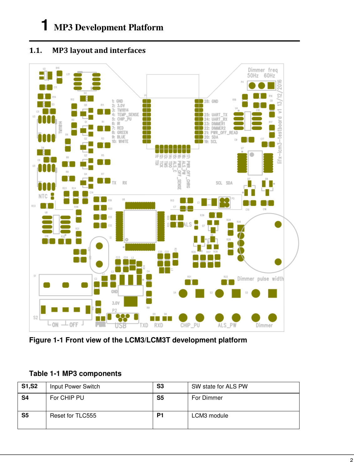
![3 P2 USB2.0 socket with 5V power input P3 MFI daughter board header P4 Jumper for selecting dimming frequency, open:50Hz, Close:60Hz U1 Voltage Regulator LM1117 U2 TM1814 Logic Translator, 74AHCT1G125SE U3, U5 TM1814, RGBW LED with SPI-mode LED driver IC on U4 TLC555 U6 FT2232HL USB-RS232 U7 74HCT221 U8 M93CxS, E2PROM D1 LED for indicator of 3.0V power D2, Q5 IR LED and its driver MOS LD1 RGBW LED IC Q1~Q4 MOS driver for RGBW LED LDR1 Ambient Light Sensor Q7 2N7002K, MOS for control Q6 Q6 SSF6007, MOS for ADC power off time sense R26 Variant Resistor 1.2. MP3 functionality This section lists the power supply, jumper settings, push button, headers interfaces and their pin assignments. Table 1-2 Power supply Table 1-3 Header interfaces Header Pin no. Function1 Function2 Function3 Function4 ESP32 GPIO no. P1 P1.1 P1.28 Ground P1.2 3.3V Power GPIO[13] P1.3 32.768k crystal positive input GPIO[12] P1.4 32.768k crystal negative input P1.5 CHIP PU GPIO[10] P1.6 VDET_1 I2C slave data GPIO[11] P1.7 VDET_2 P1.8 GREEN PWM GPIO[25] P1.9 BLUE PWM GPIO[26] P1.10 WHITE PWM GPIO[27] Component Definition and description P2 Mini-USB interface, for ART and power supply S1,S2 Input Power Switch](https://usermanual.wiki/LIFI-LABS/LCM3T/User-Guide-3608753-Page-3.png)
![4 P1.11 MTDI P1.12 MTCK P1.13 MTMS P1.14 MTDO P1.15 RED PWM GPIO[2] P1.16 IR GPIO[4] P1.17 RUN MODE P1.18 Power off time charge control GPIO[5] P1.19 SCL P1.20 SDA P1.21 Power time read control GPIO[22] P1.22 Dimmer2 GPIO[19] P1.23 Dimmer1 GPIO[21] P1.24 UART_RX P1.25 UART_TX P1.26 P1.27 NC](https://usermanual.wiki/LIFI-LABS/LCM3T/User-Guide-3608753-Page-4.png)