LM Technologies LM410 LM410 BLUETOOTH CLASS 1 MODULE WITH SMA ANTENNA User Manual LM410 Datasheetv1 1
LM Technologies Ltd. LM410 BLUETOOTH CLASS 1 MODULE WITH SMA ANTENNA LM410 Datasheetv1 1
User Manual
LM410
Page 1 of 9
+44(0) 207 428 2647 www.lm-technologies.com | sales@lm-technologies.com
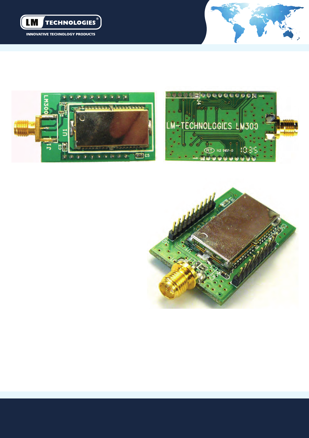
LM410 Class 1 Bluetooth SPP Plug n Play Module
External SMA Antenna, 2x10 pin connector
Product: LM410
Part No: 410-0200 for BT2.0 F/W
Datasheet Rev1.1/13-11-13
1 General Description
The LM410 is Class 1 Bluetooth2.0 + EDR module with external SMA connector. The Bluetooth funcon is based on CSR
BlueCore 04 chipset which implements full speed Class 1 bluetooth operaon with a support of upto 3 simultaneous
connecons while running full Bluetooth stack in the module. The interface to the host system is UART. This module is
suitable for serial port applicaon which require 100-600 m range (depending on the antenna) and comes with
Bluetooth 2.0+EDR compliant SPP firmware.
The default firmware is mulconnecon firmware v7.xx series and supports up to 3 simultaneous connecons
Boom View Top View
Side View
2 Features
LM410
Page 2 of 9 +44(0) 207 428 2647 www.lm-technologies.com | sales@lm-technologies.com
3 Packaging Options
• Used in LM Technologies Ltd Bluetooth Ethernet access point (LM300)
• CSR BlueCore4 chipset
• Bluetooth 2.0 + EDR support
• Full bluetooth data rate upto 3 Mbps
• Supports 3 simultaneous SPP connecons while running complete bluetooth stack in the module
• External SMA antenna connector
• Hexadecimal Command set
• LM300 Manager Windows Applicaon for Module Configuraon
• Mulpoint SPP firmware support - 3 simultaneous SPP Connecons
• 3.0 to 3.6 V operaon
• CSR Bluecore 04 (BC04) chipset
• Support 802.11 Co-existence
• RoHS Compliant
• Small Outline: 44 x 26 x 14 mm (without S MA Connector), 55 x 26 x 14 mm (with SMA connector)
• Interoperability with laptops, PDAs, Phones etc
Tray Packaging
Part No 400-0200
Product: LM410
Part No: 410-0200 for BT2.0 F/W
Datasheet Rev1.1/13-11-13
LM400 with BT2.0 + EDR mulpoint firmware v7.xx
Application
• Serial Communicaons
• Serial Device Server
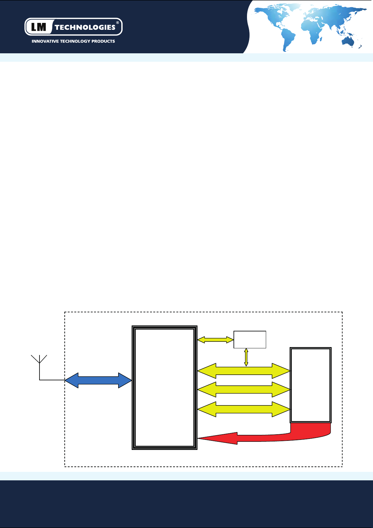
4 Block Diagram
LM072
BC04
Class 1
Module
H/W Flow
Control
Host 20
pin
Header
UART
SPI
PIO
VDD
SMA Connector
External
SMA
Antenna
LM410
Page 3 of 9
+44(0) 207 428 2647 www.lm-technologies.com | sales@lm-technologies.com
Product: LM410
Part No: 410-0200 for BT2.0 F/W
Datasheet Rev1.1/13-11-13
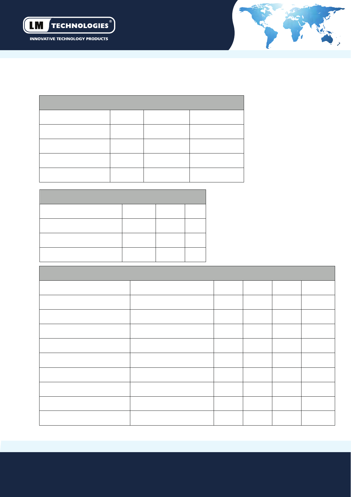
5 Electrical Characteristics
Absolute Maximum Rang
Parameter
Min
Max
Unit
Storage Temperature
-40
+85
°C
Supply Voltage (VDD) +2.7 +3.6 DCV
Supply Voltage (PVCC)
+3.0
+3.3
DCV
All other pins VSS-0.4 VDD + 0.4 DCV
Recommended Operang Condions
Parameter Min Max Unit
Storage Temperature -10 +70 °C
Supply Voltage(VDD)
+3.0
+3.6
DCV
Supply Voltage (PVCC)+3.0 +3.6 DCV
General Electrical Specificaon
Parameter Descripon Min Typical Max Unit
Carrier Frequency
2.402
2.480
GHz
RF Output power Measured with 50Ω ant 1516.518dBm
Rx Sensivity
-
-88
-86
dBm
Load Impedance No abnormal oscillaon 5:1
Input Low Voltage RESET, UART, GPIO, PCM -0.3 - 0.8DCV
Input High Voltage RESET, UART, GPIO, PCM 0.7VDD - VDD+0.3DCV
Output Low VoltageUART, GPIO, PCM - - 0.4 DCV
Output High VoltageUART, GPIO, PCM VDD-0.4 - - DCV
Average Current Consumpon Receive DM1 114 mA
LM410
Page 4 of 9
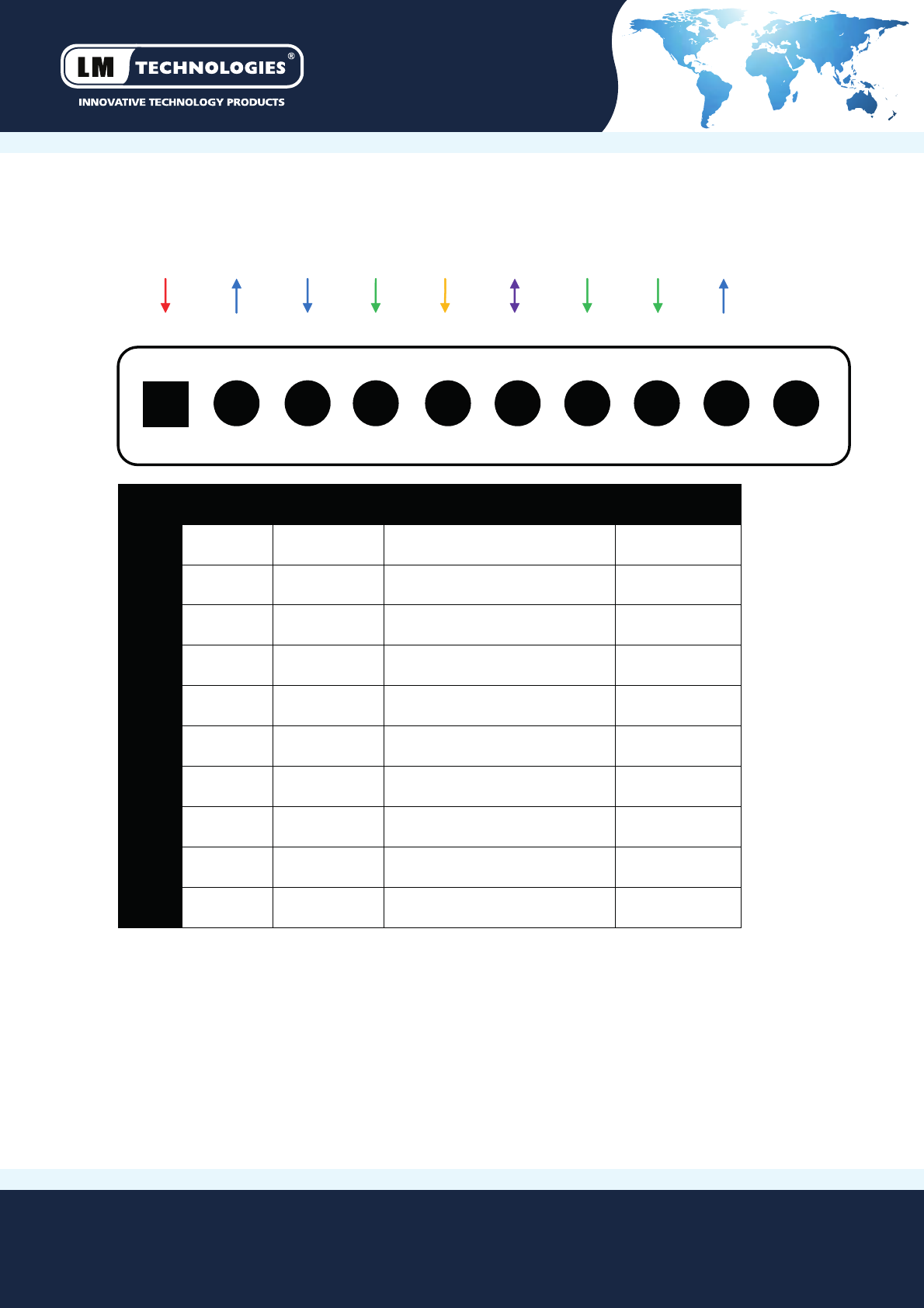
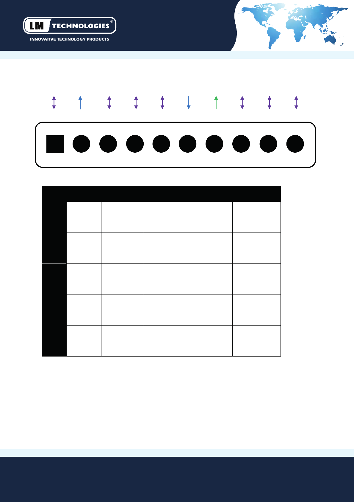
6 Pin Assignments
+44(0) 207 428 2647 www.lm-technologies.com | sales@lm-technologies.com
Product: LM410
Part No: 410-0200 for BT2.0 F/W
Datasheet Rev1.1/13-11-13
Pin Definition for Header J2
32
1
4 5 6 7 8 9 10
VDD
TXD
RXD
SPICSB
RSTL
PIO5
SPIMOSI
SPICLK
DTR
GND
Pin No
Pin name
Direcon
Descripon
Signal Level
1VDD Input DC Input (3 ~ 3.3V) Power
2TXD Output UART Data output TTL
3RXD Input UART Data Input TTL
4SPICSB Input SPI Chip Select TTL
5RSTL Input Reset (Acve Low) TTL
6PIO5 Input/output Programmable IO TTL
7SPIMOSI Input SPI Master Output Slave Input TTL
8SPICLK Input SPI Clock TTL
9DTR Output UART Data Terminal Ready TTL
10 GND Ground Ground
7 Factory Settings
The factory sengs of the COM Port are as follows:
Baud Rate: 115200 bps
Data Bits: 8
Parity: None
Stop Bits: 1
Flow Control: Hardware
LM410
Page 5 of 9
+44(0) 207 428 2647 www.lm-technologies.com | sales@lm-technologies.com
Product: LM410
Part No: 410-0200 for BT2.0 F/W
Datasheet Rev1.1/13-11-13
Pin Definition for Header J3
3
2
1
4
5
6
7
8
9
10
PIO4 RTS PIO3 PIO2 PIO7 CTS SPIMISO PIO6 PIO9 PIO8
Pin No Pin name Direcon Descripon Signal Level
1PIO4 Input/output Programmable IO TTL
2RTS Output UART Request to Send TTL
3PIO3 Input/output Programmable IO TTL
4PIO2 Input/output Programmable IO TTL
5PIO7 Input/output Programmable IO TTL
6CTS Input UART Clear to Send TTL
7SPIMISO Output SPI Master Input Slave Output TTL
8PIO6 Input/output Programmable IO TTL
9PIO9 Input/output Programmable IO TTL
10
PIO8
Input/output
Programmable IO
TTL
LM410
Page 6 of 9
+44(0) 207 428 2647 www.lm-technologies.com | sales@lm-technologies.com
Product: LM410
Part No: 410-0200 for BT2.0 F/W
Datasheet Rev1.1/13-11-13
8 Schematic
C0402C0402
C0603C0603
C0603
P40
P41
FLMD0
P06
P05
P20
P21
P22
P23
P24
P25
P26
P27
P140
P120
R0603
L0402
UART_IN
UART_OUT
UART_RTS
UART_CTS
SPIMOSI
SPIMISO
SPICLK
UART_DTR
UART_OUT
UART_IN
RESET_L
UART_DTR
UART_RTS
UART_CTS
SPIMOSI
SPICLK
SPIMISO
PIO3
PIO2
PIO5
PIO4
PIO4
PIO3
PIO2
PIO7
PIO6
PIO8
SPICSB
PIO5
PIO9
RESET_L
SPICSB
PIO6
PIO7
PIO8
PIO9
3V3
3V3
3V3
3V3
C5
100N
U1
LM072
3
4
5
6
7
8
9
10
11
12
13
14
15
16
17
18
19
20
21
22
23
24
25
26
27
28
29
30
31
32
33
34
35
36
37
38
39
40
2
1
AIO0
AIO1
PIO0
PIO1
PIO2
PIO3
PIO4
GND1
PIO5
PIO6
PIO7
PIO8
PIO9
RESET
3V3
GND2
GND3
USBDP
USBDN
PCM_SYNC
PCM_IN
PCM_OUT
PCM_CLK
UART_RX
UART_TX
UART_RTS
GND4
UART_CTS
SPIMOSI
SPICSB
SPICLK
SPIMISO
PIO11
PIO10
RFIO
GND5
GND6
GND7
+V_PA
GND0
R1
10K
C3
100N
J2
10 way
1
2
3
4
5
6
7
8
9
10
J3
10 way
1
2
3
4
5
6
7
8
9
10
L1
2N7
C1
1P5 C2
1P5
J4
6 way
1
2
3
4
5
6
J1
SMA END MOUNT
1
2
3
4
5
H
C
C
C
C
C4
100N
LM410
Page 7 of 9
+44(0) 207 428 2647 www.lm-technologies.com | sales@lm-technologies.com
Product: LM410
Part No: 410-0200 for BT2.0 F/W
Datasheet Rev1.1/13-11-13
9 Pinout from LM072 Module
Pin Number
Name
Type
Descripon
1 GND Ground Common Ground
2 PVCC Power Power Amp. Power supply (3.3V)
3AIO 0 I/O Programmable Input Output
4
AIO 1
I/O
Programmable Input Output
5PIO 0 I/O Programmable Input Output
6PIO 1 I/O Programmable Input Output
7PIO 2 I/O Programmable Input Output
8
PIO 3
I/O
Programmable Input Output
9 PIO 4 I/O Programmable Input Output
10
GND
Ground
Common Ground
11 PIO 5 I/O Programmable Input Output
12
PIO 6
I/O
Programmable Input Output
13PIO 7 I/O Programmable Input Output
14
PIO 8
I/O
Programmable Input Output
15
PIO 9
I/O
Programmable Input Output
16
RESET
CMOS Input
Reset Input of Module, Acve Low
17 VCC Power Module input Supply, 3.3V DC
18GND Ground Common Ground
19
GND
Ground
Common Ground
20
USB_DP
I/O
USB Data Plus
21 USB_DN I/O USB Data Minus
22 PCM_SYNC I/O Synchronous Data Sync
23
PCM_IN
CMOS Input
Synchronous Data Input
24
PCM_OUT
CMOS Output
Synchronous Data Output
25
PCM_CLK
I/O
Synchronous Data Clock
26 UART_RX CMOS Input UART Data Input
27
UART_TX
CMOS Output
UART Data Output
28 UART_RTS CMOS Output UART Request to Send (Acve Low)
29
GND
Ground
Common Ground
30UART_CTS CMOS Input UART Clear to Send (Acve Low)
31
SPI_MOSI
CMOS Input
Serial Peripheral Interface Data Input
32 SPI_CSB CMOS Input Chip Select for Serial Peripheral Interface (Acve Low)
33
SPI_CLK
CMOS Input
Serial Peripheral Interface Clock
34
SPI_MISO
CMOS Output
Serial Peripheral Interface Data Output
35 PIO 11 I/O Programmable Input Output
36 PIO 10 I/O Programmable Input Output
37
RF_IO
Analogue
Antenna Interface
38 GND Ground Common Ground
This device complies with the following radio frequency and safety standards.
FCC Warning
This device complies with Part 15 of the FCC Rules. Operation is
subject to the following two conditions:
(1) this device may not cause harmful interference, and (2) this device must accept any
interference received, including interference that may cause undesired operation.
NOTE 1: Any changes or modifications to this unit not expressly approved by the party
responsible for compliance could void the user's authority to operate the equipment.
FCC Radiation Exposure Statement:
This equipment complies with FCC radiation exposure limits set forth for an uncontrolled
environment. End users must follow the specific operating instructions for satisfying RF exposure
compliance.
Note 1: This module certified that complies with RF exposure requirement under mobile or fixed
condition, this module is to be installed in mobile or fixed applications.
A mobile device is defined as a transmitting device designed to be used in other than fixed
locations and to generally be used in such a way that a separation distance of at least 20
centimeters is normally maintained between the transmitter's radiating structure(s) and the body of
the user or nearby persons. Transmitting devices designed to be used by consumers or workers that
can be easily re-located, such as wireless devices associated with a personal computer, are
considered to be mobile devices if they meet the 20 centimeter separation requirement.
A fixed device is defined as a device is physically secured at one location and is not able to be
easily moved to another location.
Note 2: Any modifications made to the module will void the Grant of Certification, this module is
limited to OEM installation only and must not be sold to end-users, end-user has no manual
instructions to remove or install the device, only software or operating procedure shall be placed
in the end-user operating manual of final products.
Note 3: The device must not transmit simultaneously with any other antenna or transmitter.
Note 4: To ensure compliance with all non-transmitter functions the host manufacturer is
responsible for ensuring compliance with the module(s) installed and fully operational. For
example, if a host was previously authorized as an unintentional radiator under the Declaration of
Conformity procedure without a transmitter certified module and a module is added, the host
manufacturer is responsible for ensuring that the after the module is installed and operational the
host continues to be compliant with the Part 15B unintentional radiator requirements. Since this
may depend on the details of how the module is integrated with the host, ASK PROXIMA CO.,
LIMITED shall provide guidance to the host manufacturer for compliance with the Part 15B
requirements.
Note 5: FCC ID label on the final system must be labeled with “Contains FCC ID: VVXLM410”
or “Contains transmitter module FCC ID: VVXLM410”.
The transmitter module must be installed and used in strict accordance with the manufacturer's
instructions as described in the user documentation that comes with the host product. LM
Technologies Ltd. is responsible for the compliance of the module in all final hosts.
That separate approval is required for all other operating configurations, including portable
configurations with respect to Part 2.1093 and different antenna configurations.