Laird Connectivity AC4490-100 900 MHz Transceiver User Manual AC4424
AeroComm Corporation 900 MHz Transceiver AC4424
Users Manual
AC4490
AC4490AC4490
AC4490
900 MHz OEM TRANSCEIVERS
900 MHz OEM TRANSCEIVERS900 MHz OEM TRANSCEIVERS
900 MHz OEM TRANSCEIVERS
Specifications Subject to Change
Specifications Subject to ChangeSpecifications Subject to Change
Specifications Subject to Change
User’s Manual
User’s ManualUser’s Manual
User’s Manual
Version 1.5
Version 1.5Version 1.5
Version 1.5
10981 EICHER DRIVE
10981 EICHER DRIVE10981 EICHER DRIVE
10981 EICHER DRIVE
LENEXA, KS 66219
LENEXA, KS 66219LENEXA, KS 66219
LENEXA, KS 66219
(800) 492-2320
(800) 492-2320(800) 492-2320
(800) 492-2320
www.aerocomm.com
www.aerocomm.comwww.aerocomm.com
www.aerocomm.com
wireless@aerocomm.com
wireless@aerocomm.comwireless@aerocomm.com
wireless@aerocomm.com

2/18/03
2/18/032/18/03
2/18/03 2
22
2
DOCUMENT INFORMATION
DOCUMENT INFORMATIONDOCUMENT INFORMATION
DOCUMENT INFORMATION
Copyright
CopyrightCopyright
Copyright
Information
InformationInformation
Information Copyright © 2003 AEROCOMM, Inc. All rights reserved.
The information contained in this manual and the accompanying
software programs are copyrighted and all rights are reserved by
AEROCOMM, Inc. AEROCOMM, Inc. reserves the right to make
periodic modifications of this product without obligation to notify
any person or entity of such revision. Copying, duplicating, selling, or otherwise
distributing any part of this product without the prior consent of an authorized
representative of AEROCOMM, Inc. is prohibited.
All brands and product names in this publication are registered
trademarks or trademarks of their respective holders.
This material is preliminary
This material is preliminaryThis material is preliminary
This material is preliminary
Information furnished by AEROCOMM in this specification is believed to be accurate. Devices sold
by AEROCOMM are covered by the warranty and patent indemnification provisions appearing in its
Terms of Sale only. AEROCOMM makes no warranty, express, statutory, and implied or by
description, regarding the information set forth herein. AEROCOMM reserves the right to change
specifications at any time and without notice.
AEROCOMM’s products are intended for use in normal commercial and industrial applications.
Applications requiring unusual environmental requirements such as military, medical life-support
or life-sustaining equipment are specifically not recommended without additional testing for such
application.
Important Document Information
Important Document InformationImportant Document Information
Important Document Information
The AC4490 transceiver products are available in both commercial and industrial temperature,
noted by the character ‘C’ or ‘I’ appended to the end of the family part number. For example, the
part number for the commercial temperature version is AC4490C and the part number for the
industrial temperature version is AC4490I. The family part number will be used throughout this
document, except where specific information for the commercial or industrial temperature versions
is noted.

2/18/03
2/18/032/18/03
2/18/03 3
33
3
DOCUMENT INFORMATION
DOCUMENT INFORMATIONDOCUMENT INFORMATION
DOCUMENT INFORMATION
Revision
RevisionRevision
Revision Description
DescriptionDescription
Description
Version 1.0 3/15/2002 – Initial Release Version
Version 1.1 12/18/2002 – Preliminary Release
Version 1.2 12/20/2002 – Preliminary Release. Changed location of new interface pins for higher
compatibility with AC4424 product family.
Version 1.3 1/29/2003 – Updated interface baud rate formula/table. Updated current consumption
table. Corrected RSSI plot. Updated Interface Timeout information. Renamed product
family to AC4490. Multiple byte EEPROM read/write now allowed.
Version 1.4 2/18/2003 – Added Max Power byte. Removed Write Enable references. Fixed Power
Down/Up command response. Removed Peer-to-Peer bit. Added Auto Destination.
Added Unicast Only bit. Added 500mW product. Revised part numbers. Updated
Channel Number settings.
2/18/03
2/18/032/18/03
2/18/03 4
44
4
FCC INFORMATION
FCC INFORMATIONFCC INFORMATION
FCC INFORMATION
Agency Approval Overview
Agency Approval OverviewAgency Approval Overview
Agency Approval Overview
Part Number
Part NumberPart Number
Part Number US/FCC
US/FCCUS/FCC
US/FCC CAN/IC
CAN/ICCAN/IC
CAN/IC EUR/EN
EUR/ENEUR/EN
EUR/EN Portable
PortablePortable
Portable Mobile
MobileMobile
Mobile Fixed
FixedFixed
Fixed
AC4490-100 X X See Note 1 X-2.5cm* X-2.5cm*
* See RF Exposure warning on next page
Note 1: Specific Absorption Rating (SAR) testing required for portable applications.
Agency Identification Numbers
Agency Identification NumbersAgency Identification Numbers
Agency Identification Numbers
Part Number
Part NumberPart Number
Part Number US/FCC
US/FCCUS/FCC
US/FCC CAN/IC
CAN/ICCAN/IC
CAN/IC EUR/EN
EUR/ENEUR/EN
EUR/EN
AC4490-100 X X
FCC Notice
FCC NoticeFCC Notice
FCC Notice
Labeling Requirements
Labeling RequirementsLabeling Requirements
Labeling Requirements
Antenna Warning
Antenna WarningAntenna Warning
Antenna Warning
WARNING:
WARNING: WARNING:
WARNING: This device complies with Part 15 of the FCC Rules. Operation is subject to the
following two conditions: (1) This device may not cause harmful interference,
and (2) This device must accept any interference received, including
interference that may cause undesired operation.
WARNING:
WARNING: WARNING:
WARNING: This device has been tested with an MMCX connector with the antennas listed
below. When integrated in the OEMs product, these fixed antennas require
installation preventing end-users from replacing them with non-approved
antennas. Any antenna not in the following table must be tested to comply with
FCC Section 15.203 for unique antenna connectors and Section 15.247 for
emissions.
WARNING:
WARNING: WARNING:
WARNING: The Original Equipment Manufacturer (OEM) must ensure that FCC labeling
requirements are met. This includes a clearly visible label on the outside of the
OEM enclosure specifying the appropriate AeroComm FCC identifier for this
product as well as the FCC Notice above. The FCC identifiers are listed above
in the Agency Identifier Numbers section.

2/18/03
2/18/032/18/03
2/18/03 5
55
5
FCC INFORMATION
FCC INFORMATIONFCC INFORMATION
FCC INFORMATION
Approved Antenna List
Approved Antenna ListApproved Antenna List
Approved Antenna List
Note: We are still qualifying antennas and will add to this list as that process is completed.
Note: We are still qualifying antennas and will add to this list as that process is completed.Note: We are still qualifying antennas and will add to this list as that process is completed.
Note: We are still qualifying antennas and will add to this list as that process is completed.
Item
ItemItem
Item Part Number
Part NumberPart Number
Part Number Mfg.
Mfg.Mfg.
Mfg. Frequency
FrequencyFrequency
Frequency
Band
BandBand
Band Type
TypeType
Type Gain
GainGain
Gain
(dBi)
(dBi)(dBi)
(dBi)
AC4490X-100
AC4490X-100AC4490X-100
AC4490X-100
1 S467FL-6-RMM-915S Nearson 902 – 928MHz ½ Wave Dipole 2 PMF
2 S161AH-915R Nearson 902 – 928MHz ½ Wave Dipole 2.5 PMF
3 S331AH-915 Nearson 902 – 928MHz ¼ Wave Dipole 1 PMF
4 1020B5812-04 (Flavus 915) gigaAnt 902 – 928MHz ¼ Wave Snap-In -0.5 PMF
P=Portable, M=Mobile, F=Fixed/Basestation
P=Portable, M=Mobile, F=Fixed/BasestationP=Portable, M=Mobile, F=Fixed/Basestation
P=Portable, M=Mobile, F=Fixed/Basestation
Note: Specific Absorption Rating (SAR) testing required for portable applications.

2/18/03
2/18/032/18/03
2/18/03 6
66
6
FCC INFORMATION
FCC INFORMATIONFCC INFORMATION
FCC INFORMATION
RF Exposure AC4490-100
RF Exposure AC4490-100RF Exposure AC4490-100
RF Exposure AC4490-100
WARNING:
WARNING: WARNING:
WARNING: To comply with FCC RF Exposure requirements, the Original Equipment
Manufacturer (OEM) must ensure that the approved antenna in the previous
table must be installed and/or configured to operate with a separation distance
of 2.5cm or more from all persons to satisfy RF Exposure compliance.
The preceding statement must be included as a CAUTION statement in
manuals for products operating with the approved antennas in the previous
table to alert users on FCC RF Exposure compliance.

2/18/03
2/18/032/18/03
2/18/03 7
77
7
TABLE OF CONTENTS
TABLE OF CONTENTSTABLE OF CONTENTS
TABLE OF CONTENTS
1. OVERVIEW...................................................................................................................................... 9
2. AC4490 SPECIFICATIONS.......................................................................................................... 10
3. SPECIFICATIONS......................................................................................................................... 11
3.1 INTERFACE SIGNAL DEFINITIONS................................................................................................... 11
3.2 ELECTRICAL SPECIFICATIONS ........................................................................................................ 12
3.3 SYSTEM TIMING............................................................................................................................. 12
3.3.1 Serial Interface Data Rate .................................................................................................... 12
3.3.2 Latency Times ....................................................................................................................... 13
3.3.3 Maximum Overall System Throughput.................................................................................. 13
4. CONFIGURING THE AC4490..................................................................................................... 14
4.1 EEPROM PARAMETERS................................................................................................................ 14
4.2 EEPROM CONFIGURATION COMMANDS....................................................................................... 15
4.2.1 EEPROM Byte Read ............................................................................................................. 16
4.2.2 EEPROM Byte Write............................................................................................................. 16
4.2.3 EEPROM Exit Configuration Command .............................................................................. 16
4.3 ON-THE-FLY CONTROL COMMAND REFERENCE............................................................................ 17
4.3.1 Status Request....................................................................................................................... 17
4.3.2 Change Channel without Forced Acquisition Sync............................................................... 17
4.3.3 Change Channel with Forced Acquisition Sync.................................................................... 18
4.3.4 Server/Client Command........................................................................................................ 18
4.3.5 Sync to Channel Command................................................................................................... 19
4.3.6 Power-Down Command........................................................................................................ 19
4.3.7 Power-Down Wake-Up Command........................................................................................ 19
4.3.8 Broadcast Mode.................................................................................................................... 20
4.3.9 Write Destination Address .................................................................................................... 20
4.3.10 Read Destination Address..................................................................................................... 20
4.3.11 Read Digital Inputs............................................................................................................... 21
4.3.12 Read ADC ............................................................................................................................. 21
4.3.13 Report Last Valid RSSI ......................................................................................................... 22
4.3.14 Write Digital Outputs............................................................................................................ 22
4.3.15 Write DAC............................................................................................................................. 23
4.3.16 Set Max Power...................................................................................................................... 23
4.3.17 Transmit Buffer Empty.......................................................................................................... 24
5. THEORY OF OPERATION.......................................................................................................... 25
5.1 HARDWARE INTERFACE ................................................................................................................. 25
5.1.1 GIn (Generic Inputs 0 and 1) (pins 4 and 14 respectively) and GOn (Generic Outputs 0 and
1) (pins 1 and 9 respectively).................................................................................................................... 25
5.1.2 TXD (Transmit Data) and RXD (Receive Data) (pins 2 and 3 respectively) ........................ 25
5.1.3 Hop Frame (pin 6) ................................................................................................................ 25
5.1.4 CTS Handshaking (pin 7)...................................................................................................... 26
5.1.5 RTS Handshaking (pin 8)...................................................................................................... 26
5.1.6 9600 Baud/Packet Frame (pin 12)........................................................................................ 26
5.1.7 RSSI (pin 13)......................................................................................................................... 26
5.1.8 UP_Reset (pin 15)................................................................................................................. 27
5.1.9 Command/Data (pin 17) ....................................................................................................... 27
5.1.10 AD In and AD Out (pins 18 and 19 respectively).................................................................. 28
5.1.11 In Range (pin 20) .................................................................................................................. 28

2/18/03
2/18/032/18/03
2/18/03 8
88
8
5.2 SOFTWARE PARAMETERS............................................................................................................... 28
5.2.1 RF Architecture (Unicast/Broadcast) ................................................................................... 28
5.2.2 RF Mode ............................................................................................................................... 29
5.2.3 Sub Hop Adjust ..................................................................................................................... 29
5.2.4 Duplex Mode......................................................................................................................... 30
5.2.5 Interface Timeout/RF Packet Size......................................................................................... 30
5.2.6 Serial Interface Baud Rate.................................................................................................... 30
5.2.7 Network Topology................................................................................................................. 31
5.2.8 Frequency Offset................................................................................................................... 32
5.2.9 Auto Config........................................................................................................................... 32
5.2.10 Max Power............................................................................................................................ 33
6. APPLICATION EXAMPLES........................................................................................................ 34
7. DIMENSIONS................................................................................................................................. 35
8. ORDERING INFORMATION...................................................................................................... 36
8.1 PRODUCT PART NUMBER TREE ..................................................................................................... 36
8.2 PRODUCT PART NUMBERS............................................................................................................. 36
8.3 DEVELOPER KIT PART NUMBERS .................................................................................................. 37
Figures
FiguresFigures
Figures
Figure 1 – RSSI Voltage vs. Received Signal Strength................................................................................27
Figure 2 - AC4490 Top & Side View...........................................................................................................35
Tables
TablesTables
Tables
Table 1 – Pin Definitions..............................................................................................................................11
Table 2 – Input Voltage Characteristics........................................................................................................ 12
Table 3 – Output Voltage Characteristics.....................................................................................................12
Table 4 – Maximum Overall System Throughputs.......................................................................................13
Table 5 – EEPROM Parameters....................................................................................................................14
Table 6 – Baud Rate......................................................................................................................................31
Table 7 – US and International RF Channel Number Settings ..................................................................... 31
Table 8 – Auto Config Parameters................................................................................................................32
Table 9 – Max Power Settings......................................................................................................................33

AC4490 Specifications
AC4490 SpecificationsAC4490 Specifications
AC4490 Specifications
2/18/03
2/18/032/18/03
2/18/03 9
99
9
AC4490 Features
AC4490 FeaturesAC4490 Features
AC4490 Features
! Available in either 3.3V or 5V TTL level serial interface for fast integration
! Drop-in replacement for AC4424 2.4GHz product family1
! Two generic input and output digital lines and integrated DAC/ADC functions
! Frequency Hopping Spread Spectrum for security and interference rejection
! Cost Efficient for high volume applications
! Very low power consumption for battery powered implementations
! Small size for portable and enclosed applications
! Very Low latency and high throughput
! Industrial temperature version available (-40°C to 80°C)
1.
1.1.
1. Overview
OverviewOverview
Overview
The AC4490 is a member of AeroComm’s ConnexRF OEM transceiver family. It is designed for
integration into OEM systems operating under FCC part 15.247 regulations for the 900 MHz ISM band.
The AC4490 is a cost-effective, high performance, 900 MHz frequency hopping spread spectrum
transceiver. It provides an asynchronous TTL level serial interface for OEM Host communications.
Communications include both system and configuration data. The Host supplies system data for
transmission to other Host(s). Configuration data is stored in an on-board EEPROM. All frequency
hopping, synchronization, and RF system data transmission/reception is performed by the transceiver.
The AC4490 transceivers can be used as a direct serial cable replacement – requiring no special Host
software for operation. They also feature a number of On-the-Fly Control Commands providing the
OEM Host with a very versatile interface for any situation.
AC4490 transceivers operate in a Point-to-Point or Point-to-Multipoint, Client-Server or Peer-to-Peer
architecture. One transceiver is configured as a Server and there can be one or many Clients. To
establish synchronization between transceivers, the Server emits a beacon. Upon detecting a beacon,
a Client transceiver informs its Host and a RF link is established.
This document contains information about the hardware and software interface between an
AeroComm AC4490 transceiver and an OEM Host. Information includes the theory of operation,
specifications, interface definition, configuration information and mechanical drawing.
The OEM is responsible for ensuring the final product meets all FCC and/or appropriate regulatory
agency requirements listed herein before selling any product.
1 See AC4424/AC4490 Integration Guide for details

AC4490 Specifications
AC4490 SpecificationsAC4490 Specifications
AC4490 Specifications
2/18/03
2/18/032/18/03
2/18/03 10
1010
10
2.
2.2.
2. AC4490 Specifications
AC4490 SpecificationsAC4490 Specifications
AC4490 Specifications
GENERAL
GENERALGENERAL
GENERAL
Interface 20 pin mini-connector
Serial Interface Data Rate PC baud rates from 1200 bps to 115,200 bps
Power Consumption (typical) Duty Cycle (TX=Transmit; RX=Receive)
Duty Cycle (TX=Transmit; RX=Receive)Duty Cycle (TX=Transmit; RX=Receive)
Duty Cycle (TX=Transmit; RX=Receive)
10%TX
10%TX10%TX
10%TX
50%TX
50%TX50%TX
50%TX
100%TX
100%TX100%TX
100%TX
100%RX
100%RX100%RX
100%RX
Pwr-Down
Pwr-DownPwr-Down
Pwr-Down
AC4490-100: 43mA 95mA 160mA 30mA TBD
Channels (used to create independent networks) 5 Channel Sets comprising 58 total channels
Security One byte System ID
RADIO
RADIORADIO
RADIO
Frequency Band US/Canada: 902 – 928 MHz
Australia: 915 – 928 MHz
Radio Type Frequency Hopping Spread Spectrum
Output Power (conducted, no antenna) AC4490-100: 50mW typical
Effective Isotropic Radiated Power (EIRP with
3dBi gain antenna) AC4490-100: 100mW typical
Voltage 3.3 or 3.3 - 6V ±2%, ±50mV ripple
Sensitivity -100dBm typical
Range (based on 3dBi gain antenna) AC4490-100: 10,000 ft.
ENVIRONMENTAL
ENVIRONMENTALENVIRONMENTAL
ENVIRONMENTAL
Temperature (Operating) Commercial:
Industrial: AC4490C: 0°C to 60°C
AC4490I: -40°C to 80°C
Temperature (Storage) -50°C to +85°C
Humidity (non-condensing) 10% to 90%
PHYSICAL
PHYSICALPHYSICAL
PHYSICAL
Dimensions 1.65” x 1.9” x 0.20”
Antenna AC4490-100: MMCX Jack or Integral Antenna
Weight Less than 0.75 ounce

AC4490 Specifications
AC4490 SpecificationsAC4490 Specifications
AC4490 Specifications
2/18/03
2/18/032/18/03
2/18/03 11
1111
11
3.
3.3.
3. Specifications
SpecificationsSpecifications
Specifications
3.1
3.13.1
3.1 I
IIINTERFACE
NTERFACE NTERFACE
NTERFACE S
SS
SIGNAL
IGNAL IGNAL
IGNAL D
DD
DEFINITIONS
EFINITIONSEFINITIONS
EFINITIONS
The AC4490 has a simple interface that allows OEM Host communications with the transceiver. Table 1
Table 1Table 1
Table 1
– Pin Definitions
– Pin Definitions– Pin Definitions
– Pin Definitions, shows the connector pin numbers and associated functions. The I/O direction is with
respect to the transceiver. All outputs are 3.3VDC levels and inputs are 5VDC TTL with the exception of
RSSI, AD In and AD Out, which are all analog. All inputs are weakly pulled High and may be left floating
during normal operation.
Table
Table Table
Table 1
11
1 –
– –
– Pin Definitions
Pin DefinitionsPin Definitions
Pin Definitions
Pin
PinPin
Pin Type
TypeType
Type Signal Name
Signal NameSignal Name
Signal Name Function
FunctionFunction
Function
1 O GO0 Interruptible Generic Output pin
2 O TXD Transmitted data out of the transceiver
3 I RXD Data input to the transceiver
4 I GI0 Interruptible Generic Input pin
5 GND GND Signal Ground
6 O Hop Frame Active Low when the transceiver is hopping.
7 O CTS Clear to Send – Active Low when the transceiver is ready to accept data for transmission.
8 I RTS Request to Send – When enabled in EEPROM, active Low when the OEM Host is ready to
accept data from the transceiver. NOTE: Keeping RTS High for too long can cause data loss.
9 O GO1 Generic Output pin
10 PWR VCC 3.3 or 3.3 – 6V ± 2%, ± 50mV ripple
11 PWR VCC 3.3 or 3.3 – 6V ± 2%, ±50 mV ripple
12 I 9600_BAUD 9600_BAUD – When pulled logic Low before applying power or resetting the transceiver’s
serial interface is forced to a 9600, 8, N, 1 rate. To exit, transceiver must be reset or power-
cycled with 9600_Baud logic High.
13 O RSSI Received Signal Strength - An analog output giving a relative indication of received signal
strength while in Receive Mode
14 I GI1 Generic Input pin
15 I UP_RESET RESET – Controlled by the AC4490 for power-on reset if left unconnected. After a Stable
power-on, a logic High pulse will reset the AC4490. Do not power-up the transceiver with this
pin tied Low.
16 GND GND Signal Ground
17 I Command/Data When logic Low, transceiver interprets Host data as command data. When logic High,
transceiver interprets Host data as transmit data.
18 I AD In Analog Data Input
19 O AD Out Analog Data Output
20 O IN_RANGE In Range – Active Low when a Client radio is in range of a Server on same Channel with the same
System ID.
I = Input to the transceiver O = Output from the transceiver

AC4490 Specifications
AC4490 SpecificationsAC4490 Specifications
AC4490 Specifications
2/18/03
2/18/032/18/03
2/18/03 12
1212
12
3.2
3.23.2
3.2 E
EE
ELECTRICAL
LECTRICAL LECTRICAL
LECTRICAL S
SS
SPECIFICATIONS
PECIFICATIONSPECIFICATIONS
PECIFICATIONS
Table
Table Table
Table 2
22
2 – Input Voltage Characteristics
– Input Voltage Characteristics – Input Voltage Characteristics
– Input Voltage Characteristics
Pin
PinPin
Pin Type
TypeType
Type Name
NameName
Name High Min.
High Min.High Min.
High Min. High Max.
High Max.High Max.
High Max. Low Min.
Low Min.Low Min.
Low Min. Low Max.
Low Max.Low Max.
Low Max. Unit
UnitUnit
Unit
3 I RXD 2 5.5 0 0.8 V @ 5µA
4 I GI0 2 5.5 0 0.8 V @ 5µA
8 I RTS 2 5.5 0 0.8 V @ 5µA
12 I 9600_Baud 2 5.5 0 0.8 V @ 5µA
14 I GI1 2 5.5 0 0.8 V @ 5µA
15 I UP_RESET 0.8 5.5 0 0.6 V @ 5µA
17 I Command/Data 2 5.5 0 0.8 V @ 5µA
18 I AD In N/A 3.3 0 N/A V @ 1µA
Table
Table Table
Table 3
33
3 – Output Voltage Characteristics
– Output Voltage Characteristics – Output Voltage Characteristics
– Output Voltage Characteristics
Pin
PinPin
Pin Type
TypeType
Type Name
NameName
Name High Min.
High Min.High Min.
High Min. Low Max.
Low Max.Low Max.
Low Max. Unit
UnitUnit
Unit
1 O GO0 2.5 @ 8mA 0.4 @ 8mA V
2 O TXD 2.5 @ 2mA 0.4 @ 2mA V
6 O Hop Frame 2.5 @ 2mA 0.4 @ 2mA V
7 O CTS 2.5 @ 2mA 0.4 @ 2mA V
9 O GO1 2.5 @ 2mA 0.4 @ 2mA V
12 O Packet Frame 2.5 @ 2mA 0.4 @ 2mA V
13 O RSSI See Figure 1 See Figure 1 V
19 O AD Out N/A N/A V2
20 O IN_RANGE 2.5 @ 2mA 0.4 @ 2mA V
3.3
3.33.3
3.3 S
SS
SYSTEM
YSTEM YSTEM
YSTEM T
TT
TIMING
IMINGIMING
IMING
Care should be taken when selecting transceiver architecture as it can have serious effects on data
rates, latency timings, and overall system throughput. The importance of these three characteristics
will vary from system to system and should be a strong consideration when designing the system.
3.3.1
3.3.13.3.1
3.3.1
Serial Interface Data Rate
Serial Interface Data RateSerial Interface Data Rate
Serial Interface Data Rate
The Serial Interface Data Rate is programmable by the Host. This is the rate the Host and transceiver
communicate over the serial bus. Possible values range from 1200 bps to 115,200 bps. The only
supported mode is asynchronous – 8-bit, No Parity, 1 Start Bit, and 1 Stop Bit.
..
.
2 AD Out is an unbuffered, high impedance output and must be buffered by the OEM Host when used.

AC4490 Specifications
AC4490 SpecificationsAC4490 Specifications
AC4490 Specifications
2/18/03
2/18/032/18/03
2/18/03 13
1313
13
3.3.2
3.3.23.3.2
3.3.2
Latency Times
Latency TimesLatency Times
Latency Times
TBD
3.3.3
3.3.33.3.3
3.3.3
Maximum Overall System Throughput
Maximum Overall System Throughput Maximum Overall System Throughput
Maximum Overall System Throughput
When configured as shown in the table below, an AC4490 transceiver is capable
capable capable
capable of achieving the listed
throughput. However, in the presence of interference or at longer ranges, the transceiver may not be
able to meet these specified throughputs.
Table
Table Table
Table 4
44
4 – Maximum Overall System Throughputs
– Maximum Overall System Throughputs – Maximum Overall System Throughputs
– Maximum Overall System Throughputs
RF Mode Interface Baud
Rate Duplex FEC Direction Throughput
(bps)
Stream 57.6k Half Disabled One way TBD
Stream 57.6k Half Enabled One way TBD
Acknowledge 57.6k Half Disabled One way TBD
Acknowledge 57.6k Full Disabled Both ways TBD

AC4490 Specifications
AC4490 SpecificationsAC4490 Specifications
AC4490 Specifications
2/18/03
2/18/032/18/03
2/18/03 14
1414
14
4.
4.4.
4. Configuring the AC4490
Configuring the AC4490Configuring the AC4490
Configuring the AC4490
4.1
4.14.1
4.1 EEPROM P
EEPROM PEEPROM P
EEPROM PARAMETERS
ARAMETERSARAMETERS
ARAMETERS
A Host can program various parameters that are stored in EEPROM and become active after a power-
on reset. Table 5 - EEPROM Parameters
Table 5 - EEPROM ParametersTable 5 - EEPROM Parameters
Table 5 - EEPROM Parameters, gives the locations and descriptions of the parameters that
can be read or written by a Host. Factory default values are also shown.
Do not write to any EEPROM
Do not write to any EEPROMDo not write to any EEPROM
Do not write to any EEPROM
addresses other than those listed below. Do not copy a transceiver’s EEPROM data to another
addresses other than those listed below. Do not copy a transceiver’s EEPROM data to anotheraddresses other than those listed below. Do not copy a transceiver’s EEPROM data to another
addresses other than those listed below. Do not copy a transceiver’s EEPROM data to another
transceiver. Doing so may cause the transceiver to malfunction.
transceiver. Doing so may cause the transceiver to malfunction.transceiver. Doing so may cause the transceiver to malfunction.
transceiver. Doing so may cause the transceiver to malfunction.
Table
Table Table
Table 5
55
5 – EEPROM Parameters
– EEPROM Parameters – EEPROM Parameters
– EEPROM Parameters
Parameter
ParameterParameter
Parameter EEPROM
EEPROMEEPROM
EEPROM
Address
AddressAddress
Address Length
LengthLength
Length
(Bytes)
(Bytes)(Bytes)
(Bytes) Range
RangeRange
Range Default
DefaultDefault
Default Description
DescriptionDescription
Description
Product ID 00H 40
40 bytes - Product identifier string.
Includes revision information for
software and hardware.
Sub Hop Adjust 36H 1 00 – FFh 66h This value should only be changed
when recommended by Aerocomm
Channel
Number 40H 1 00 – 39h 00h
Set 0 = 00 – 0Fh (US/Canada)
Set 1 = 10 – 2Fh (US/Canada)
Set 2 = 30 – 37h (Australia)
Set 3 = 38h (France High Power)
Set 4 = 39h (France Low Power)
Server/Client
Mode 41H 1 01 – 02h 02h 01h = Server
02h = Client
Baud Rate Low 42H 1 00 – FFh FCh Low Byte of the interface baud rate.
Baud Rate High 43H 1 00h 00h Always 00h
Control 0 45H 1 00010100b
(14h) Settings are:
Bit 7 – AeroComm Use Only
AeroComm Use OnlyAeroComm Use Only
AeroComm Use Only
Bit 6 – AeroComm Use Only
AeroComm Use OnlyAeroComm Use Only
AeroComm Use Only
Bit 5 – Sync to Channel
0 = Don't Sync to Channel
1 = Sync to Channel
Bit 4 – AeroComm Use Only
AeroComm Use OnlyAeroComm Use Only
AeroComm Use Only
Bit 3 – Packet Frame
0 = Disable Packet Frame
1 = Use pin 12 as Packet Frame
Bit 2 – RF Mode
0 = RF Stream Mode
1 = RF Acknowledge Mode
Bit 1 – RF Delivery
0 = Addressed
1 = Broadcast
Bit 0 – FEC
0 = No Forward Error Correction
1 = Use Forward Error Correction

AC4490 Specifications
AC4490 SpecificationsAC4490 Specifications
AC4490 Specifications
2/18/03
2/18/032/18/03
2/18/03 15
1515
15
Parameter
ParameterParameter
Parameter EEPROM
EEPROMEEPROM
EEPROM
Address
AddressAddress
Address Length
LengthLength
Length
(Bytes)
(Bytes)(Bytes)
(Bytes) Range
RangeRange
Range Default
DefaultDefault
Default Description
DescriptionDescription
Description
Frequency
Offset 46H 1 00 – FFh 00h
Transmit
Retries 4CH 1 01 – FFh 10h
Broadcast
Attempts 4DH 1 01 – FFh 04h
API Control 56H 1 01000011b
(43h) Settings are:
Bit 7 – AeroComm Use Only
AeroComm Use OnlyAeroComm Use Only
AeroComm Use Only
Bit 6 – AeroComm Use Only
AeroComm Use OnlyAeroComm Use Only
AeroComm Use Only
Bit 5 – Unicast Only
0 = Receive Unicast and Broadcast
packets
1 = Only receive Unicast packets
Bit 4 – Auto Destination
0 = Use Destination Address
1 = Set Destination to Server
Bit 3 – AeroComm Use Only
AeroComm Use OnlyAeroComm Use Only
AeroComm Use Only
Bit 2 – RTS Enable
0 = RTS Ignored
1 = Transceiver obeys RTS
Bit 1 – Duplex Mode
0 = Half Duplex
1 = Full Duplex
Bit 0 – Auto Config
0 = Use EEPROM values
1 = Auto Configure Values
Interface
Timeout 58H 1 02 – FFh 04h
Sync Channel 5AH 1 00 – 3Fh 01h
RF Packet Size 5BH 1 01 – 40h 46h
CTS On 5CH 1 01 – FFh D2h
CTS On
Hysteresis 5DH 1 01 – FFh ACh
Max Power 63H 1 00 – FFh 60h
Destination ID 70H 6 6 Bytes
System ID 76H 1 00 – FFh 01h
MAC ID 80H 6 6 Bytes Unique IEEE MAC Address
4.2
4.24.2
4.2 EEPROM C
EEPROM CEEPROM C
EEPROM CONFIGURATION
ONFIGURATION ONFIGURATION
ONFIGURATION C
CC
COMMANDS
OMMANDSOMMANDS
OMMANDS
The configuration set allows the Host to modify the operation of the transceiver. If the Command/Data
pin (Pin 17) is pulled logic Low, a transceiver will interpret incoming Host data as Command Data. The
Host can then read and write parameters using the various configuration commands listed below. To
exit Configuration Mode, the Host must perform a hardware or power-on reset or issue an Exit
Command Mode command to the transceiver.

AC4490 Specifications
AC4490 SpecificationsAC4490 Specifications
AC4490 Specifications
2/18/03
2/18/032/18/03
2/18/03 16
1616
16
4.2.1
4.2.14.2.1
4.2.1
EEPROM Byte Read
EEPROM Byte ReadEEPROM Byte Read
EEPROM Byte Read
Upon receiving this command, a transceiver will transmit the desired data from the address requested
by the Host.
Host Command:
Host Command:Host Command:
Host Command:
Byte 1 = C0h
Byte 2 = Address
Byte 3 = Length (01…FFh = 1…255 bytes; 00h = 256 bytes)
Transceiver Response:
Transceiver Response:Transceiver Response:
Transceiver Response:
Byte 1 = C0h
Byte 2 = Address
Byte 3 = Length
Byte 4…n = Data at requested address(s)
4.2.2
4.2.24.2.2
4.2.2
EEPROM Byte Write
EEPROM Byte WriteEEPROM Byte Write
EEPROM Byte Write
Upon receiving this command, a transceiver will write the data byte to the address specified but will not
echo it back to the Host until the EEPROM write cycle is complete. The write can take as long as
10ms to complete. Following the write cycle, a transceiver will transmit the data byte to the Host.
Multiple byte EEPROM writes are allowed up to a length of 128 bytes. An EEPROM boundary exists
between addresses 7Fh and 80h. No single EEPROM write command shall write to addresses on
both sides of that EEPROM boundary.
Host Command:
Host Command:Host Command:
Host Command:
Byte 1 = C1h
Byte 2 = Address
Byte 3 = Length (01 – 80h)
Byte 4…n = Data to store at Address
Transceiver Response:
Transceiver Response:Transceiver Response:
Transceiver Response:
Byte 1 = C1h
Byte 2 = Address
Byte 3 = Length (01 – 80h)
Byte 4 = Last data byte written by this command
4.2.3
4.2.34.2.3
4.2.3
EEPROM Exit Configuration Command
EEPROM Exit Configuration CommandEEPROM Exit Configuration Command
EEPROM Exit Configuration Command
The OEM Host can cause the transceiver to exit command mode by issuing the Exit Configuration
Command mode command to the transceiver. However, the transceiver will not reflect any of the
However, the transceiver will not reflect any of theHowever, the transceiver will not reflect any of the
However, the transceiver will not reflect any of the
changes programmed into the EEPROM until the transceiver is reset.
changes programmed into the EEPROM until the transceiver is reset.changes programmed into the EEPROM until the transceiver is reset.
changes programmed into the EEPROM until the transceiver is reset.
Host Command:
Host Command:Host Command:
Host Command:
Byte 1 = 56h
Transceiver Response:
Transceiver Response:Transceiver Response:
Transceiver Response:
Byte 1 = 56h

AC4490 Specifications
AC4490 SpecificationsAC4490 Specifications
AC4490 Specifications
2/18/03
2/18/032/18/03
2/18/03 17
1717
17
4.3
4.34.3
4.3 O
OO
ON
NN
N-
--
-THE
THETHE
THE-F
-F-F
-FLY
LY LY
LY C
CC
CONTROL
ONTROL ONTROL
ONTROL C
CC
COMMAND
OMMAND OMMAND
OMMAND R
RR
REFERENCE
EFERENCEEFERENCE
EFERENCE
The AC4490 transceiver contains static memory that holds many of the parameters that control the
transceiver operation. Using the “CC” command set allows many of these parameters to be changed
during system operation. Because the memory these commands affect is static, when the transceiver
is reset, these parameters will revert back to the settings stored in the EEPROM. Do not to modify
Do not to modifyDo not to modify
Do not to modify
undocumented static addresses as undesired operation may occur. All “CC” commands must be
undocumented static addresses as undesired operation may occur. All “CC” commands must beundocumented static addresses as undesired operation may occur. All “CC” commands must be
undocumented static addresses as undesired operation may occur. All “CC” commands must be
issued from the Host to the transceiver with Command/Data (Pin 17) pulled logic Low. To exit “CC”
issued from the Host to the transceiver with Command/Data (Pin 17) pulled logic Low. To exit “CC”issued from the Host to the transceiver with Command/Data (Pin 17) pulled logic Low. To exit “CC”
issued from the Host to the transceiver with Command/Data (Pin 17) pulled logic Low. To exit “CC”
mode, simply take the Command/Data pin High.
mode, simply take the Command/Data pin High.mode, simply take the Command/Data pin High.
mode, simply take the Command/Data pin High.
4.3.1
4.3.14.3.1
4.3.1
Status Request
Status RequestStatus Request
Status Request
The Host issues this command to request the status of the transceiver.
Host Command:
Host Command:Host Command:
Host Command:
Byte 1 = CCh
Byte 2 = 00h
Byte 3 = 00h
Transceiver Response:
Transceiver Response:Transceiver Response:
Transceiver Response:
Byte 1 = CCh
Byte 2 = Firmware version number
Byte 3 = Data1
Where:
Where:Where:
Where:
Data1 =
00 for Server in Normal Operation
01 for Client in Normal Operation
02 for Server in Acquisition Sync
03 for Client in Acquisition Sync
4.3.2
4.3.24.3.2
4.3.2
Change Channel without Forced Acquisition Sync
Change Channel without Forced Acquisition SyncChange Channel without Forced Acquisition Sync
Change Channel without Forced Acquisition Sync
The Host issues this command to change the channel of the transceiver. The transceiver will not begin
acquisition sync until its Range Refresh timer expires.
Host Command:
Host Command:Host Command:
Host Command:
Byte 1 = CCh
Byte 2 = 01h
Byte 3 = RF Channel Number (Hexadecimal)
Transceiver Response:
Transceiver Response:Transceiver Response:
Transceiver Response:
Byte 1 = CCh
Byte 2 = RF Channel Number (Hexadecimal)

AC4490 Specifications
AC4490 SpecificationsAC4490 Specifications
AC4490 Specifications
2/18/03
2/18/032/18/03
2/18/03 18
1818
18
4.3.3
4.3.34.3.3
4.3.3
Change Channel with Forced Acquisition Sync
Change Channel with Forced Acquisition SyncChange Channel with Forced Acquisition Sync
Change Channel with Forced Acquisition Sync
The Host issues this command to change the channel of the transceiver and force the transceiver to
immediately begin synchronization.
Host Command:
Host Command:Host Command:
Host Command:
Byte 1 = CCh
Byte 2 = 02h
Byte 3 = RF Channel Number (Hexadecimal)
Transceiver Response:
Transceiver Response:Transceiver Response:
Transceiver Response:
Byte 1 = CCh
Byte 2 = RF Channel Number (Hexadecimal)
4.3.4
4.3.44.3.4
4.3.4
Server/Client Command
Server/Client CommandServer/Client Command
Server/Client Command
The Host issues this command to change the mode (Server or Client) of the transceiver and can force
the transceiver to actively begin synchronization.
Host Command:
Host Command:Host Command:
Host Command:
Byte 1 = CCh
Byte 2 = 03h
Byte 3 = Data1
Where:
Where:Where:
Where:
Data1 =
00 for Server in Normal Operation
01 for Client in Normal Operation
02 for Server in Acquisition Sync
03 for Client in Acquisition Sync
Transceiver Response:
Transceiver Response:Transceiver Response:
Transceiver Response:
Byte 1 = CCh
Byte 2 = Software Version Number
Byte 3 = Data1
Where:
Where:Where:
Where:
Data1 = Data1 from Host Command

AC4490 Specifications
AC4490 SpecificationsAC4490 Specifications
AC4490 Specifications
2/18/03
2/18/032/18/03
2/18/03 19
1919
19
4.3.5
4.3.54.3.5
4.3.5
Sync to Channel Command
Sync to Channel CommandSync to Channel Command
Sync to Channel Command
The Host issues this command to change the Sync Channel
Sync ChannelSync Channel
Sync Channel byte. This will only affect operation when
Sync to Channel
Sync to ChannelSync to Channel
Sync to Channel is enabled in the EEPROM
Host Command:
Host Command:Host Command:
Host Command:
Byte 1 = CCh
Byte 2 = 05h
Byte 3 = Data1
Where:
Where:Where:
Where:
Data1 = New Sync Channel
Transceiver Response:
Transceiver Response:Transceiver Response:
Transceiver Response:
Byte 1 = CCh
Byte 2 = 05h
Byte 3 = Data1
Where:
Where:Where:
Where:
Data1 = Data1 from Host Command
4.3.6
4.3.64.3.6
4.3.6
Power-Down Command
Power-Down CommandPower-Down Command
Power-Down Command
After the Host issues the power-down command to the transceiver, the transceiver will de-assert the
In_Range line after entering power-down. A Client transceiver in power-down will remain in sync with a
Server for a minimum of 2 minutes. To maintain synchronization with the Server, this Client transceiver
should re-sync to the Server at least once every 2 minutes. This re-sync is accomplished by issuing
the Power-Down Wake-Up Command
Power-Down Wake-Up CommandPower-Down Wake-Up Command
Power-Down Wake-Up Command and waiting for the In Range line to go active. Once this occurs,
the Client transceiver is in sync with the Server and can be put back into power-down.
Host Command:
Host Command:Host Command:
Host Command:
Byte 1 = CCh
Byte 2 = 06h
Transceiver Response:
Transceiver Response:Transceiver Response:
Transceiver Response:
Byte 1 = CCh
Byte 2 = RF Channel Number
4.3.7
4.3.74.3.7
4.3.7
Power-Down Wake-Up Command
Power-Down Wake-Up CommandPower-Down Wake-Up Command
Power-Down Wake-Up Command
The Power-Down Wake-Up Command is issued by the Host to bring the transceiver out of power-
down mode.
Host Command:
Host Command:Host Command:
Host Command:
Byte 1 = CCh
Byte 2 = 07h
Transceiver Response:
Transceiver Response:Transceiver Response:
Transceiver Response:
Byte 1 = CCh
Byte 2 = RF Channel Number

AC4490 Specifications
AC4490 SpecificationsAC4490 Specifications
AC4490 Specifications
2/18/03
2/18/032/18/03
2/18/03 20
2020
20
4.3.8
4.3.84.3.8
4.3.8
Broadcast Mode
Broadcast ModeBroadcast Mode
Broadcast Mode
The Host issues this command to change the transceiver operation between Addressed Mode
Addressed ModeAddressed Mode
Addressed Mode and
Broadcast Mode
Broadcast ModeBroadcast Mode
Broadcast Mode. If addressed mode is selected the transceiver will send all packets to the radio
designated by the Destination Address
Destination AddressDestination Address
Destination Address programmed in the transceiver.
Host Command:
Host Command:Host Command:
Host Command:
Byte 1 = CCh
Byte 2 = 08h
Byte 3 = 00 for addressed mode, 01 for broadcast mode
Transceiver Response:
Transceiver Response:Transceiver Response:
Transceiver Response:
Byte 1 = CCh
Byte 2 = 00 for addressed mode, 01 for broadcast mode
4.3.9
4.3.94.3.9
4.3.9
Write Destination Address
Write Destination AddressWrite Destination Address
Write Destination Address
The Host issues this command to the transceiver to change the Destination Address. This is a very
veryvery
very
powerful
powerful powerful
powerful command that provides the OEM Host with a means for ad-hoc networking. Only the three
Only the threeOnly the three
Only the three
Least Significant Bytes of the MAC Address are used for packet delivery.
Least Significant Bytes of the MAC Address are used for packet delivery.Least Significant Bytes of the MAC Address are used for packet delivery.
Least Significant Bytes of the MAC Address are used for packet delivery.
Host Command:
Host Command:Host Command:
Host Command:
Byte 1 = CCh
Byte 2 = 10h
Bytes 3 – 5 = 00 – FFh corresponding the three LSB’s of the destination MAC Address
Transceiver Response:
Transceiver Response:Transceiver Response:
Transceiver Response:
Byte 1 = CCh
Bytes 2 – 4= 00 – FFh corresponding the three LSB’s of the destination MAC Address
4.3.10
4.3.104.3.10
4.3.10
Read Destination Address
Read Destination AddressRead Destination Address
Read Destination Address
The Host issues this command to the transceiver to read the Destination Address. This is a very
veryvery
very
powerful
powerful powerful
powerful command that provides the OEM Host with a means for ad-hoc networking. Only the three
Only the threeOnly the three
Only the three
Least Significant Bytes of the MAC Address are used for packet delivery.
Least Significant Bytes of the MAC Address are used for packet delivery.Least Significant Bytes of the MAC Address are used for packet delivery.
Least Significant Bytes of the MAC Address are used for packet delivery.
Host Command:
Host Command:Host Command:
Host Command:
Byte 1 = CCh
Byte 2 = 11h
Transceiver Response:
Transceiver Response:Transceiver Response:
Transceiver Response:
Byte 1 = CCh
Bytes 2 – 4= 00 – FFh corresponding the three LSB’s of the destination MAC Address

AC4490 Specifications
AC4490 SpecificationsAC4490 Specifications
AC4490 Specifications
2/18/03
2/18/032/18/03
2/18/03 21
2121
21
4.3.11
4.3.114.3.11
4.3.11
Read Digital Inputs
Read Digital InputsRead Digital Inputs
Read Digital Inputs
The Host issues this command to read both digital input lines.
Host Command:
Host Command:Host Command:
Host Command:
Byte 1 = CCh
Byte 2 = 20h
Transceiver Response:
Transceiver Response:Transceiver Response:
Transceiver Response:
Byte 1 = CCh
Byte 2 = Data1
Where:
Where:Where:
Where:
Data1 = bit 0 – GI0, bit 1 – GI1
4.3.12
4.3.124.3.12
4.3.12
Read ADC
Read ADCRead ADC
Read ADC
The Host issues this command to read any of the three onboard A/D converters.
Host Command:
Host Command:Host Command:
Host Command:
Byte 1 = CCh
Byte 2 = 21h
Byte 3 = Data1
Where:
Where:Where:
Where:
Data1 = 00h – AD In, 01h – Temperature, 02h – RSSI
Transceiver Response:
Transceiver Response:Transceiver Response:
Transceiver Response:
Byte 1 = CCh
Byte 2 = Data1
Byte 3 = Data2
Where:
Where:Where:
Where:
Data1 = MSB of requested 12 bit ADC value
Data2 = LSB of requested 12 bit ADC value

AC4490 Specifications
AC4490 SpecificationsAC4490 Specifications
AC4490 Specifications
2/18/03
2/18/032/18/03
2/18/03 22
2222
22
4.3.13
4.3.134.3.13
4.3.13
Report Last Valid RSSI
Report Last Valid RSSIReport Last Valid RSSI
Report Last Valid RSSI
As RSSI values are only valid when the local radio is receiving a RF packet from a remote radio,
instantaneous RSSI can be very tricky to use. Therefore, the transceiver stores the most recent valid
RSSI value. The Host issues this command to request that value. Note: This value will default to FFh if
no valid RSSI measurement has been made.
Host Command:
Host Command:Host Command:
Host Command:
Byte 1 = CCh
Byte 2 = 22h
Transceiver Response:
Transceiver Response:Transceiver Response:
Transceiver Response:
Byte 1 = CCh
Byte 2 = Data1
Where:
Where:Where:
Where:
Data1 = Most significant 8 bits of last valid RSSI reading.
4.3.14
4.3.144.3.14
4.3.14
Write Digital Outputs
Write Digital OutputsWrite Digital Outputs
Write Digital Outputs
The Host issues this command to write both digital output lines to particular states.
Host Command:
Host Command:Host Command:
Host Command:
Byte 1 = CCh
Byte 2 = 23h
Transceiver Response:
Transceiver Response:Transceiver Response:
Transceiver Response:
Byte 1 = CCh
Byte 2 = Data1
Where:
Where:Where:
Where:
Data1 = bit 0 – GO0, bit 1 – GO1

AC4490 Specifications
AC4490 SpecificationsAC4490 Specifications
AC4490 Specifications
2/18/03
2/18/032/18/03
2/18/03 23
2323
23
4.3.15
4.3.154.3.15
4.3.15
Write DAC
Write DACWrite DAC
Write DAC
The Host issues this command to write AD Out to a particular voltage. NOTE: AD Out is an unbuffered,
high impedance output and must be buffered
must be bufferedmust be buffered
must be buffered by the OEM Host when used.
Host Command:
Host Command:Host Command:
Host Command:
Byte 1 = CCh
Byte 2 = 24h
Byte 3 = Data1
Byte 4 = Data2
Where:
Where:Where:
Where:
Data1 = Update Period where: TUpdate = (255 * (Data1 + 1)) / 14.7256+06
Data2 = Duty Cycle where: Vout = (Data2 / 100h) * Vcc
Transceiver Response:
Transceiver Response:Transceiver Response:
Transceiver Response:
Byte 1 = CCh
Byte 2 = Data1
Byte 3 = Data2
Where:
Where:Where:
Where:
Data1 = Data1 from Host Command
Data2 = Data2 from Host Command
4.3.16
4.3.164.3.16
4.3.16
Set Max Power
Set Max PowerSet Max Power
Set Max Power
The Host Issues this command to limit the maximum transmit power emitted by the transceiver. This
can be useful to minimize current consumption and satisfy certain regulatory requirements.
Host Command:
Host Command:Host Command:
Host Command:
Byte 1 = CCh
Byte 2 = 25h
Byte 3 = Data1
Where:
Where:Where:
Where:
Data1 = New Max Power
Max PowerMax Power
Max Power
Transceiver Response:
Transceiver Response:Transceiver Response:
Transceiver Response:
Byte 1 = CCh
Byte 2 = Data1
Where:
Where:Where:
Where:
Data1 = Data1 from Host Command

AC4490 Specifications
AC4490 SpecificationsAC4490 Specifications
AC4490 Specifications
2/18/03
2/18/032/18/03
2/18/03 24
2424
24
4.3.17
4.3.174.3.17
4.3.17
Transmit Buffer Empty
Transmit Buffer EmptyTransmit Buffer Empty
Transmit Buffer Empty
The Host issues this command to determine when the RF Transmit buffer is empty. The Host will not
receive the transceiver response until that time.
Host Command:
Host Command:Host Command:
Host Command:
Byte 1 = CCh
Byte 2 = 30h
Transceiver Response:
Transceiver Response:Transceiver Response:
Transceiver Response:
Byte 1 = CCh
Byte 2 = 00h

AC4490 Specifications
AC4490 SpecificationsAC4490 Specifications
AC4490 Specifications
2/18/03
2/18/032/18/03
2/18/03 25
2525
25
5.
5.5.
5. Theory of Operation
Theory of OperationTheory of Operation
Theory of Operation
5.1
5.15.1
5.1 H
HH
HARDWARE INTERFACE
ARDWARE INTERFACEARDWARE INTERFACE
ARDWARE INTERFACE
Below is a description of all hardware pins used to control the AC4490.
5.1.1
5.1.15.1.1
5.1.1
GIn (Generic Inputs 0 and 1) (pins 4 and 14 respectively) and GOn
GIn (Generic Inputs 0 and 1) (pins 4 and 14 respectively) and GOnGIn (Generic Inputs 0 and 1) (pins 4 and 14 respectively) and GOn
GIn (Generic Inputs 0 and 1) (pins 4 and 14 respectively) and GOn
(Generic Outputs 0 and 1) (pins 1 and 9 respectively)
(Generic Outputs 0 and 1) (pins 1 and 9 respectively)(Generic Outputs 0 and 1) (pins 1 and 9 respectively)
(Generic Outputs 0 and 1) (pins 1 and 9 respectively)
Both GIn pins, when enabled in EEPROM, serve as negative-going edge triggered generic input pins.
Both GOn pins, when enabled in EEPROM, serve as generic output pins. The following functions can
be accomplished with these pins.
GIn/GOn Options:
GIn/GOn Options:GIn/GOn Options:
GIn/GOn Options:
1) A negative-going edge is detected on either GIn pin. The state of both pins is transmitted over
the RF (as configured by RF Mode
RF ModeRF Mode
RF Mode) and will be presented to corresponding GOn pins on the
remote radio(s).
2) A “CC” command is issued to force an update on remote radio’s GOn pins. The state of both
local GIn lines is transmitted over the RF (as configured by RF Mode
RF ModeRF Mode
RF Mode) and will be presented to
corresponding Gon pins on the remote radio(s).
3) The
Read Digital Inputs
Read Digital Inputs Read Digital Inputs
Read Digital Inputs
“CC” command is issued to read the state of both GIn pins locally
(details can be found in the
On-the-Fly Control Command Reference
On-the-Fly Control Command ReferenceOn-the-Fly Control Command Reference
On-the-Fly Control Command Reference
).
4) The
Write Digital Outputs
Write Digital Outputs Write Digital Outputs
Write Digital Outputs
“CC” command is issued to write all GOn pins locally to particular
states (details can be found in the
On-the-Fly Control Command Reference
On-the-Fly Control Command ReferenceOn-the-Fly Control Command Reference
On-the-Fly Control Command Reference
).
5) A “CC” command is issued to write the GOn pins on a remote radio to particular states.
Those states are transmitted over the RF (as configured by RF Mode
RF ModeRF Mode
RF Mode) and will be presented to
the corresponding pins on the remote radio(s).
5.1.2
5.1.25.1.2
5.1.2
TXD (Transmit Data) and RXD (Receive Data) (pins 2 and 3 respectively)
TXD (Transmit Data) and RXD (Receive Data) (pins 2 and 3 respectively)TXD (Transmit Data) and RXD (Receive Data) (pins 2 and 3 respectively)
TXD (Transmit Data) and RXD (Receive Data) (pins 2 and 3 respectively)
The AC4490 accepts 3.3 or 5VDC TTL level asynchronous serial data on the RXD pin and interprets
that data as either Command Data or Transmit Data. Data is sent from the transceiver to the OEM Host
via the TXD pin. The data must be of the format 8-N-1 (8 data bits, No Parity bits, One stop bit).
5.1.3
5.1.35.1.3
5.1.3
Hop Frame (pin 6)
Hop Frame (pin 6)Hop Frame (pin 6)
Hop Frame (pin 6)
The AC4490 is a frequency hopping spread spectrum radio. Frequency hopping allows the system to
hop around interference in order to provide a better wireless link. Hop Frame transitions logic Low at
the start of a hop and transitions logic High at the completion of a hop. The OEM Host is not required
to monitor Hop Frame.

AC4490 Specifications
AC4490 SpecificationsAC4490 Specifications
AC4490 Specifications
2/18/03
2/18/032/18/03
2/18/03 26
2626
26
5.1.4
5.1.45.1.4
5.1.4
CTS Handshaking (pin 7)
CTS Handshaking (pin 7)CTS Handshaking (pin 7)
CTS Handshaking (pin 7)
The AC4490 has an interface buffer size of 256 bytes. If the buffer fills up and more bytes are sent to
the transceiver before the buffer can be emptied, data corruption will occur. The transceiver prevents
this corruption by asserting CTS High as the buffer fills up and taking CTS Low as the buffer is
emptied. CTS On
CTS OnCTS On
CTS On in conjunction with CTS On Hysteresis
CTS On HysteresisCTS On Hysteresis
CTS On Hysteresis control the operation of CTS. CTS On
specifies the amount of bytes that must be in the buffer for CTS to be disabled (High). Even while CTS
is disabled, the OEM Host can still send data to the transceiver, but it should do so carefully. Once
CTS is disabled, it will remain disabled until the buffer is reduced to the size specified by CTS On
Hysteresis.
5.1.5
5.1.55.1.5
5.1.5
RTS Handshaking (pin 8)
RTS Handshaking (pin 8)RTS Handshaking (pin 8)
RTS Handshaking (pin 8)
With RTS Mode
RTS ModeRTS Mode
RTS Mode disabled, the transceiver will send any received packet to the OEM Host as soon as
the packet is received. However, some OEM Hosts are not able to accept data from the transceiver all
of the time. With RTS Mode Enabled, the OEM Host can keep the transceiver from sending it a packet
by disabling RTS (logic High). Once RTS is enabled (logic Low), the transceiver can send packets to
the OEM Host as they are received. Note: Leaving RTS disabled for too long can cause data loss
Note: Leaving RTS disabled for too long can cause data lossNote: Leaving RTS disabled for too long can cause data loss
Note: Leaving RTS disabled for too long can cause data loss
once the transceiver’s receive buffer fills up.
once the transceiver’s receive buffer fills up.once the transceiver’s receive buffer fills up.
once the transceiver’s receive buffer fills up.
5.1.6
5.1.65.1.6
5.1.6
9600 Baud/Packet Frame (pin 12)
9600 Baud/Packet Frame (pin 12)9600 Baud/Packet Frame (pin 12)
9600 Baud/Packet Frame (pin 12)
9600_BAUD
9600_BAUD9600_BAUD
9600_BAUD – When pulled logic Low before applying power or resetting, the transceiver’s serial
interface is forced to a 9600, 8-N-1 (8 data bits, No parity, 1 stop bit) rate. To exit, transceiver must be
reset or power-cycled with 9600_Baud logic High.
Packet Frame
Packet FramePacket Frame
Packet Frame – When enabled in EEPROM, Packet Frame will transition logic Low at the start of a
received RF packet and transition logic High at the completion of the packet.
5.1.7
5.1.75.1.7
5.1.7
RSSI (pin 13)
RSSI (pin 13)RSSI (pin 13)
RSSI (pin 13)
Instantaneous RSSI
Instantaneous RSSIInstantaneous RSSI
Instantaneous RSSI
Received Signal Strength Indicator is used by the Host as an indication of instantaneous signal
strength at the receiver. The Host must calibrate RSSI without a RF signal being presented to the
receiver. Calibration is accomplished by following the steps listed below to find a minimum and
maximum voltage value.
1) Power up only one Client (no Server) transceiver in the coverage area.
2) Measure the RSSI signal to obtain the minimum value with no other signal present.
3) Power up a Server. Make sure the two transceivers are in close proximity and measure
the Client’s peak RSSI once the Client reports In Range to obtain a maximum value at full
signal strength.

AC4490 Specifications
AC4490 SpecificationsAC4490 Specifications
AC4490 Specifications
2/18/03
2/18/032/18/03
2/18/03 27
2727
27
Validated RSSI
Validated RSSIValidated RSSI
Validated RSSI
As RSSI values are only valid when the local radio is receiving a RF packet from a remote radio,
instantaneous RSSI can be very tricky to use. Therefore, the transceiver stores the most recent valid
RSSI value. The Host issues the
Report Last Good RSSI
Report Last Good RSSI Report Last Good RSSI
Report Last Good RSSI
command to request that value (details can
be found in the
On-the-Fly Control Command Reference
On-the-Fly Control Command ReferenceOn-the-Fly Control Command Reference
On-the-Fly Control Command Reference
). Validated RSSI is not available at the RSSI
pin.
Figure
Figure Figure
Figure 1
11
1 – RSSI Voltage vs. Received Signal Strength
– RSSI Voltage vs. Received Signal Strength – RSSI Voltage vs. Received Signal Strength
– RSSI Voltage vs. Received Signal Strength
5.1.8
5.1.85.1.8
5.1.8
UP_Reset (pin 15)
UP_Reset (pin 15)UP_Reset (pin 15)
UP_Reset (pin 15)
UP_Reset provides a direct connection to the reset pin on the AC4490 microprocessor. To guarantee
a valid power-up reset, this pin should never be tied Low on power-up. For a valid power-on reset,
reset must be High for a minimum of 50us.
5.1.9
5.1.95.1.9
5.1.9
Command/Data (pin 17)
Command/Data (pin 17)Command/Data (pin 17)
Command/Data (pin 17)
When logic High, transceiver interprets Host data as transmit data to be sent to other transceivers and
their Hosts. When logic Low, transceiver interprets Host data as command data (see section 4)
(see section 4)(see section 4)
(see section 4).
0
0.2
0.4
0.6
0.8
1
1.2
-105 -100 -95 -90 -85 -80 -75 -70 -65 -60 -55 -50
Signal at Receiver (dBm)
Voltage (VDC)

AC4490 Specifications
AC4490 SpecificationsAC4490 Specifications
AC4490 Specifications
2/18/03
2/18/032/18/03
2/18/03 28
2828
28
5.1.10
5.1.105.1.10
5.1.10
AD In and AD Out (pins 18 and 19 respectively)
AD In and AD Out (pins 18 and 19 respectively)AD In and AD Out (pins 18 and 19 respectively)
AD In and AD Out (pins 18 and 19 respectively)
When enabled in EEPROM, AD In and AD Out can be used as a cost savings to replace Analog-to-
Digital and Digital-to-Analog converter hardware. The following conditions are all possible when
enabled in EEPROM. Note: AD Out is an unbuffered, high impedance output and must be buffered
must be bufferedmust be buffered
must be buffered by
the OEM Host when used.
1) A refresh rate can be programmed in EEPROM to cause a transceiver to read the AD In port
and send the state of that port over the RF (as configured by RF Mode
RF ModeRF Mode
RF Mode) and will be presented
to the AD Out pin on the remote radio(s).
2) A “CC” command is issued to cause a transceiver to read the AD In port locally and send the
state of that port over the RF (as configured by RF Mode
RF ModeRF Mode
RF Mode) and will be presented to the AD Out
pin on the remote radio(s).
3) The
Read ADC
Read ADCRead ADC
Read ADC
command is issued to read the state of AD In locally (details can be found in
the
On-the-Fly Control Command Reference
On-the-Fly Control Command ReferenceOn-the-Fly Control Command Reference
On-the-Fly Control Command Reference
).
4) The
Write ADC
Write ADCWrite ADC
Write ADC
command is issued to write the AD Out pin to a particular state locally (details
can be found in the
On-the-Fly Control Command Reference
On-the-Fly Control Command ReferenceOn-the-Fly Control Command Reference
On-the-Fly Control Command Reference
).
6) A “CC” command is issued to write the AD Out pin on a remote radio(s) to a particular state.
This state is transmitted over the RF (as configured by RF Mode
RF ModeRF Mode
RF Mode) and will be presented to the
AD Out pin on the remote radio(s).
5.1.11
5.1.115.1.11
5.1.11
In Range (pin 20)
In Range (pin 20)In Range (pin 20)
In Range (pin 20)
The IN_RANGE pin at the connector will be driven logic Low when a Client is in range of a Server on
the same RF Channel
RF ChannelRF Channel
RF Channel and System ID
System IDSystem ID
System ID. If a Client cannot hear a Server for 7.5s, it will drive the
IN_RANGE pin logic High and enter a search mode looking for a Server. As soon as it detects a
Server, the IN_RANGE pin will be driven logic Low. A Server Host can determine which Clients are in
range by the Server’s Host software polling a Client’s Host.
5.2
5.25.2
5.2 S
SS
SOFTWARE
OFTWARE OFTWARE
OFTWARE P
PP
PARAMETERS
ARAMETERSARAMETERS
ARAMETERS
Below is a description of all software parameters used to control the AC4490.
5.2.1
5.2.15.2.1
5.2.1
RF Architecture (Unicast/Broadcast)
RF Architecture (Unicast/Broadcast)RF Architecture (Unicast/Broadcast)
RF Architecture (Unicast/Broadcast)
The Server controls the system timing by sending out regular beacons (transparent to the transceiver
Host) which contain system timing information. This timing information synchronizes the Client radios
to the Server.
Each network should consist of only one Server. There should never be two Servers on the same RF
RFRF
RF
Channel Number
Channel NumberChannel Number
Channel Number in the same coverage area, as the interference between the two Servers will severely
hinder RF communications.
The AC4490 runs a Peer-to-Peer type architecture where all transceivers, whether Servers or Clients,
can communicate with all other transceivers. To prohibit transceivers from receiving broadcast
packets, Unicast Only
Unicast OnlyUnicast Only
Unicast Only can be enabled.

AC4490 Specifications
AC4490 SpecificationsAC4490 Specifications
AC4490 Specifications
2/18/03
2/18/032/18/03
2/18/03 29
2929
29
5.2.2
5.2.25.2.2
5.2.2
RF Mode
RF ModeRF Mode
RF Mode
All radios located on the same network must use the same RF Mode.
All radios located on the same network must use the same RF Mode.All radios located on the same network must use the same RF Mode.
All radios located on the same network must use the same RF Mode.
RF Delivery Overview
RF Delivery OverviewRF Delivery Overview
RF Delivery Overview
All packets are sent out over the RF as either addressed or broadcast packets. Addressed packets are
only received by the radio specified by Destination Address
Destination AddressDestination Address
Destination Address. If addressed packets are desired, the
Destination Address
should be programmed with the MAC ID
MAC IDMAC ID
MAC ID of the destination radio. To simplify
EEPROM programming, Auto Destination
Auto DestinationAuto Destination
Auto Destination can be enabled in Clients which allows the Client to
automatically set its Destination Address to the address of the Server. Broadcast packets are sent out
to every eligible transceiver on the network. If broadcast packets are desired, RF Delivery
RF DeliveryRF Delivery
RF Delivery should be
set to Broadcast.
Acknowledge Mode
Acknowledge ModeAcknowledge Mode
Acknowledge Mode
In Addressed Acknowledge Mode, the RF packet is sent out to the receiver designated by the
Destination Address
Destination AddressDestination Address
Destination Address. Transmit Retries
Transmit RetriesTransmit Retries
Transmit Retries is used to increase the odds of successful delivery to the
intended receiver. Transparent to the OEM Host, the sending transceiver will send the RF packet to
the intended receiver. If the receiver receives the packet free of errors, it will tell the sender. If the
sender does not receive this acknowledge, it will assume the packet was never received and retry the
packet. This will go on until the packet is successfully received or the transmitter exhausts all of its
retries. The received packet will only be sent to the OEM Host if and when it is received free of errors.
In Broadcast Acknowledge Mode, the RF packet is broadcast out to all eligible receivers on the
network. In order to increase the odds of successful delivery, Broadcast Attempts
Broadcast AttemptsBroadcast Attempts
Broadcast Attempts is used to increase
the odds of successful delivery to the intended receiver(s). Transparent to the OEM Host, the sending
transceiver will send the RF packet to the intended receiver. If the receiver detects a packet error, it will
throw out the packet. This will go on until the packet is successfully received or the transmitter
exhausts all of its attempts. Once the receiver successfully receives the packet it will send the packet
to the OEM Host. It will throw out any duplicates caused by further Broadcast Attempts. The received
packet will only be sent to the OEM Host if it is received free of errors.
Stream Mode
Stream ModeStream Mode
Stream Mode
In Broadcast Stream mode, the RF packet is broadcast out to all eligible receivers on the network. In
Addressed Stream Mode, the RF packet is sent out to the receiver designated by the Destination
DestinationDestination
Destination
Address
AddressAddress
Address. The sending transceiver will send each RF packet out once. There are no retries on the
packet. Whether or not the packet contains errors, the receiver(s) will send the packet to the OEM
Host. However, if receiver is not able to receive the packet in its entirety (there are bytes missing), it will
not send the packet to the OEM Host. In order to increase the odds of successful delivery, Forward
ForwardForward
Forward
Error Correction (FEC)
Error Correction (FEC)Error Correction (FEC)
Error Correction (FEC) may be used. FEC is used (transparent to the OEM Host) to increase the odds
of correctly receiving a packet sent over the RF. When enabled, the transceiver will send every byte
over the RF 3 times and then perform a best-of-three bit-wise decision on the received bytes. Enabling
FEC can cut overall throughput by 1/3. Note: All transceivers on the same network must have the
Note: All transceivers on the same network must have theNote: All transceivers on the same network must have the
Note: All transceivers on the same network must have the
same setting for FEC. Stream Mode is incompatible with Full Duplex Mode.
same setting for FEC. Stream Mode is incompatible with Full Duplex Mode.same setting for FEC. Stream Mode is incompatible with Full Duplex Mode.
same setting for FEC. Stream Mode is incompatible with Full Duplex Mode.
5.2.3
5.2.35.2.3
5.2.3
Sub Hop Adjust
Sub Hop AdjustSub Hop Adjust
Sub Hop Adjust
Sub Hop Adjust is an AC4490 protocol parameter and should only be modified at the recommendation
of Aerocomm.

AC4490 Specifications
AC4490 SpecificationsAC4490 Specifications
AC4490 Specifications
2/18/03
2/18/032/18/03
2/18/03 30
3030
30
5.2.4
5.2.45.2.4
5.2.4
Duplex Mode
Duplex ModeDuplex Mode
Duplex Mode
In Half Duplex mode, the AC4490 will send a packet out over the RF when it can. This can cause
packets sent at the same time by a Server and a Client to collide with each other over the RF. To
prevent this, Full Duplex Mode can be enabled. This mode restricts Clients to transmitting on odd
numbered frequency “bins” and the Server to transmitting on even frequency bins. Though the RF
hardware is still technically half duplex, it makes the radio seem full duplex. This can cause overall
throughputs to be cut in half. Note: All transceivers on the same network must have the same setting
Note: All transceivers on the same network must have the same settingNote: All transceivers on the same network must have the same setting
Note: All transceivers on the same network must have the same setting
for Full Duplex. Full Duplex mode is incompatible with Stream RF mode.
for Full Duplex. Full Duplex mode is incompatible with Stream RF mode.for Full Duplex. Full Duplex mode is incompatible with Stream RF mode.
for Full Duplex. Full Duplex mode is incompatible with Stream RF mode.
5.2.5
5.2.55.2.5
5.2.5
Interface Timeout/RF Packet Size
Interface Timeout/RF Packet SizeInterface Timeout/RF Packet Size
Interface Timeout/RF Packet Size
Interface timeout, in conjunction with RF Packet Size
RF Packet SizeRF Packet Size
RF Packet Size, determines when a buffer of data will be sent out
over the RF as a complete RF packet based on whichever condition occurs first.
Interface Timeout
Interface TimeoutInterface Timeout
Interface Timeout – Interface Timeout specifies a maximum byte gap in between consecutive bytes.
When that byte gap is exceeded, the bytes in the transmit buffer are sent out over the RF as a
complete packet. Interface timeout is adjustable in 1ms increments and has a tolerance of ±1ms.
Therefore, the Interface Timeout should be set to a minimum of 2. The default value for Interface
Timeout is 4 or 4ms.
RF Packet Size
RF Packet Size RF Packet Size
RF Packet Size – When the amount of bytes in the transceiver transmit buffer equals RF Packet Size,
those bytes are sent out as a complete RF packet.
5.2.6
5.2.65.2.6
5.2.6
Serial Interface Baud Rate
Serial Interface Baud RateSerial Interface Baud Rate
Serial Interface Baud Rate
This two-byte value determines the baud rate used for communicating over the serial interface to a
transceiver. Table 5 - Baud Rate/Timeout
Table 5 - Baud Rate/TimeoutTable 5 - Baud Rate/Timeout
Table 5 - Baud Rate/Timeout lists values for some common baud rates. Baud rates below
1200 baud are not supported. For a baud rate to be valid, the calculated baud rate must be within ±3%
of the OEM Host baud rate. If the 9600_BAUD pin (Pin 12) is pulled logic Low at reset, the baud rate
If the 9600_BAUD pin (Pin 12) is pulled logic Low at reset, the baud rateIf the 9600_BAUD pin (Pin 12) is pulled logic Low at reset, the baud rate
If the 9600_BAUD pin (Pin 12) is pulled logic Low at reset, the baud rate
will be forced to 9,600
will be forced to 9,600will be forced to 9,600
will be forced to 9,600.
. .
. For Baud Rate values other than those shown in Table 5 - Baud Rate
Table 5 - Baud RateTable 5 - Baud Rate
Table 5 - Baud Rate, the
following equation can be used:
BAUD = 100h - (14.7456E
BAUD = 100h - (14.7456EBAUD = 100h - (14.7456E
BAUD = 100h - (14.7456E+06
+06 +06
+06 / (64 * desired baud rate))
/ (64 * desired baud rate))/ (64 * desired baud rate))
/ (64 * desired baud rate))
BaudH= Always 0
BaudH= Always 0BaudH= Always 0
BaudH= Always 0
BaudL = Low 8 bits of BAUD (base16)
BaudL = Low 8 bits of BAUD (base16)BaudL = Low 8 bits of BAUD (base16)
BaudL = Low 8 bits of BAUD (base16)

AC4490 Specifications
AC4490 SpecificationsAC4490 Specifications
AC4490 Specifications
2/18/03
2/18/032/18/03
2/18/03 31
3131
31
Table
Table Table
Table 6
66
6 – Baud Rate
– Baud Rate – Baud Rate
– Baud Rate
Baud
BaudBaud
Baud
Rate
RateRate
Rate BaudL
BaudLBaudL
BaudL
(42h)
(42h)(42h)
(42h) BaudH
BaudHBaudH
BaudH
(43h)
(43h)(43h)
(43h) Minimum Interface Timeout
Minimum Interface TimeoutMinimum Interface Timeout
Minimum Interface Timeout
(58h)
(58h)(58h)
(58h)
115,200 FEh 00h 02h
57,600 FCh 00h 02h
38,400 FAh 00h 02h
28,800 F8h 00h 02h
19,200 F4h 00h 02h
14,400 F0h 00h 03h
9,600 E8h 00h 03h
4800 D0h 00h 05h
2400 A0h 00h 09h
1200 40h 00h 11h
5.2.7
5.2.75.2.7
5.2.7
Network Topology
Network TopologyNetwork Topology
Network Topology
RF Channel Number
RF Channel NumberRF Channel Number
RF Channel Number – RF Channel Number provides a physical separation between co-located
networks. The AC4490 is a spread spectrum frequency hopping radio with a fixed hopping sequence.
Without synchronizing the different networks to each other, different channel numbers could possibly
interfere with each other and create “cross-talk.” To avoid cross-talk interference, co-located networks
should use Sync-to-Channel
Sync-to-ChannelSync-to-Channel
Sync-to-Channel. A Server radio with Sync-to-Channel enabled will synchronize its
frequency hop timing to a system located on the RF Channel specified by Sync Channel
Sync ChannelSync Channel
Sync Channel. The only
requirement is that Sync Channel be numerically less than RF Channel. Therefore, every co-located
network will be synchronizing to the network with the lowest RF Channel. Four Channel sets are
provided for the AC4490. Co-located networks must use the same Channel Set.
Co-located networks must use the same Channel Set.Co-located networks must use the same Channel Set.
Co-located networks must use the same Channel Set.
Table
Table Table
Table 7
77
7 – US and International RF Channel Number Settings
– US and International RF Channel Number Settings – US and International RF Channel Number Settings
– US and International RF Channel Number Settings
Channel Set RF Channel Number Range
(40h) Frequency Details and Regulatory
Requirements Countries
0 0 – 0Fh 902 – 928MHz (26 hop bins) US/Canada
1 10 – 2Fh 902 – 928MHz (50 hop bins) US/Canada
2 30 – 37h 915 – 928MHz Australia
3 38h 869.4 – 869.5MHz (Up to 500mW at 10%
maximum transmit vs. receive duty cycle) France
4 39h 869.7 – 870MHz (Up to 5mW with no duty
cycle requirement) France
System ID
System IDSystem ID
System ID – System ID is similar to a password character or network number and makes network
eavesdropping more difficult. A receiving radio will not go in range of or communicate with another
radio on a different System ID.

AC4490 Specifications
AC4490 SpecificationsAC4490 Specifications
AC4490 Specifications
2/18/03
2/18/032/18/03
2/18/03 32
3232
32
5.2.8
5.2.85.2.8
5.2.8
Frequency Offset
Frequency OffsetFrequency Offset
Frequency Offset
Frequency Offset is an AC4490 protocol parameter and should only be modified at the
recommendation of Aerocomm.
5.2.9
5.2.95.2.9
5.2.9
Auto Config
Auto ConfigAuto Config
Auto Config
The AC4490 has several variables that control its RF performance and vary by RF Mode
RF ModeRF Mode
RF Mode and RF
RFRF
RF
Architecture
ArchitectureArchitecture
Architecture. Enabling Auto Config will bypass the value for these variables stored in EEPROM and use
predetermined values for the given Interface Baud Rate. Auto Config has been optimized for 115,200
Auto Config has been optimized for 115,200Auto Config has been optimized for 115,200
Auto Config has been optimized for 115,200
baud Acknowledge Mode and all lower baud rates. It should only be disabled with recommendation
baud Acknowledge Mode and all lower baud rates. It should only be disabled with recommendationbaud Acknowledge Mode and all lower baud rates. It should only be disabled with recommendation
baud Acknowledge Mode and all lower baud rates. It should only be disabled with recommendation
from AeroComm.
from AeroComm.from AeroComm.
from AeroComm. Below is a list containing some of the variables affected by Auto Config and their
respective values:
Table
Table Table
Table 8
88
8 – Auto Config Parameters
– Auto Config Parameters – Auto Config Parameters
– Auto Config Parameters
Parameter Auto Config Value
RF Packet Size 46h
CTS On D2h
CTS On Hysteresis ACh

AC4490 Specifications
AC4490 SpecificationsAC4490 Specifications
AC4490 Specifications
2/18/03
2/18/032/18/03
2/18/03 33
3333
33
5.2.10
5.2.105.2.10
5.2.10
Max Power
Max PowerMax Power
Max Power
Max Power provides a means for controlling the RF transmit output power of the AC4490. The
following table lists some common values for Max Power and their current consumption. Output
power and current consumption can vary by as much as ±10% per radio.
Table
Table Table
Table 9
99
9 – Max Power Settings
– Max Power Settings – Max Power Settings
– Max Power Settings
Max Power (Address 63h) 100% Transmit Current (mA) Transmit Power Output(dBm)
00h 47 -20
01h 50 -10
02h 50.5 -3
03h 52 1
04h 55 4
05h 58.5 7
06h 63.5 9
07h 69 10.5
08h 76 12
09h 83 13.5
0Ah 90.5 14.5
0Bh 97.5 15.5
0Ch 105 16.5
0Dh 111.5 17

AC4490 Specifications
AC4490 SpecificationsAC4490 Specifications
AC4490 Specifications
2/18/03
2/18/032/18/03
2/18/03 34
3434
34
6.
6.6.
6. Application Examples
Application ExamplesApplication Examples
Application Examples
TBD
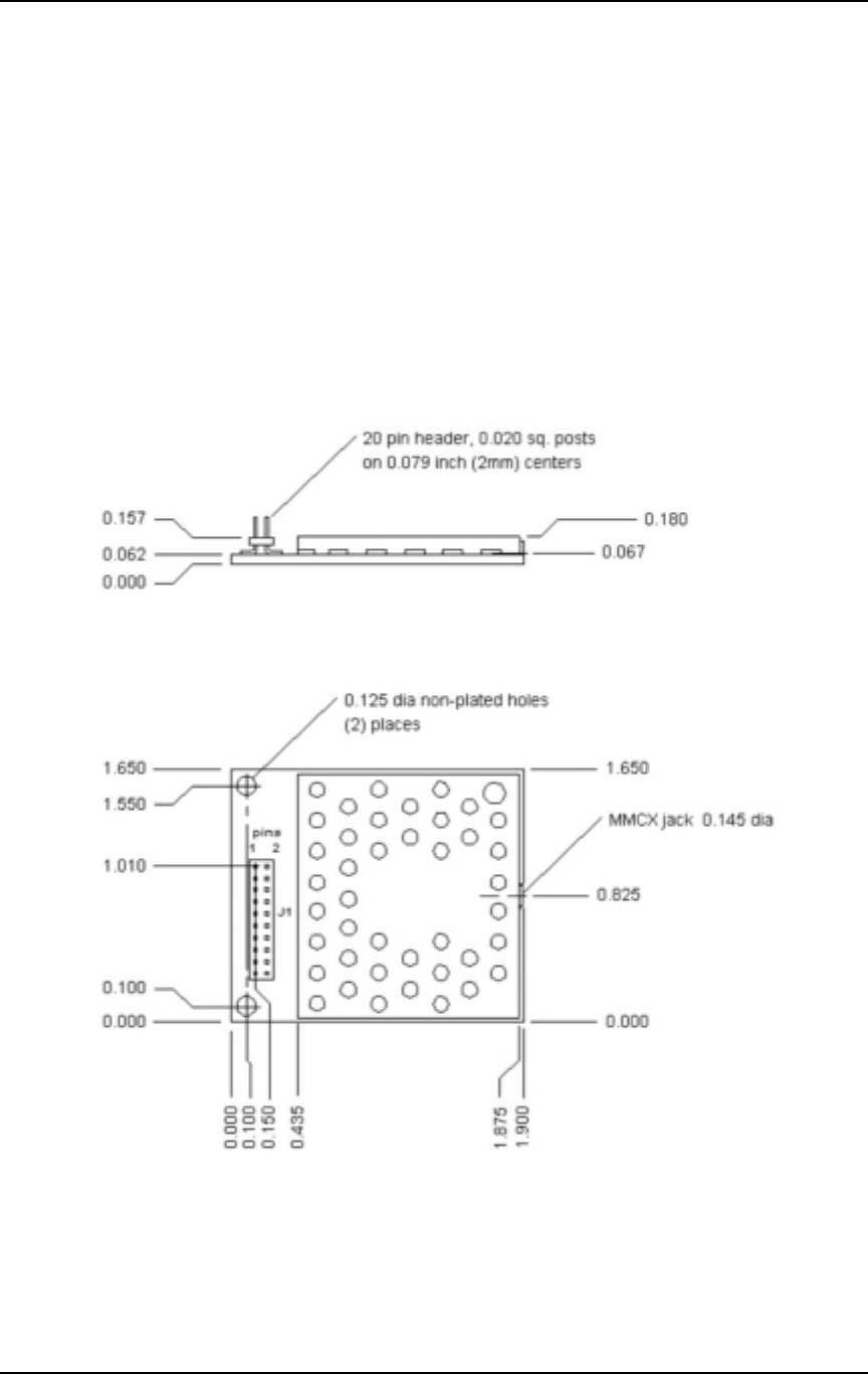
AC4490 Specifications
AC4490 SpecificationsAC4490 Specifications
AC4490 Specifications
2/18/03
2/18/032/18/03
2/18/03 35
3535
35
7.
7.7.
7. Dimensions
DimensionsDimensions
Dimensions
All AC4490 products measure 1.9”L x 1.65”W. Critical parameters are as follows:
• J1
J1J1
J1 – 20 pin OEM interface connector (Samtec TMM-110-01-L-D-SM, mates with Samtec
SMM-110-02-S-D)
• MMCX Jack
MMCX JackMMCX Jack
MMCX Jack – Antenna connector (Telegartner P/N J01341C0081) mates with any
manufacturer’s MMCX plug
Figure
Figure Figure
Figure 2
22
2 - AC4490 Top & Side View
- AC4490 Top & Side View - AC4490 Top & Side View
- AC4490 Top & Side View
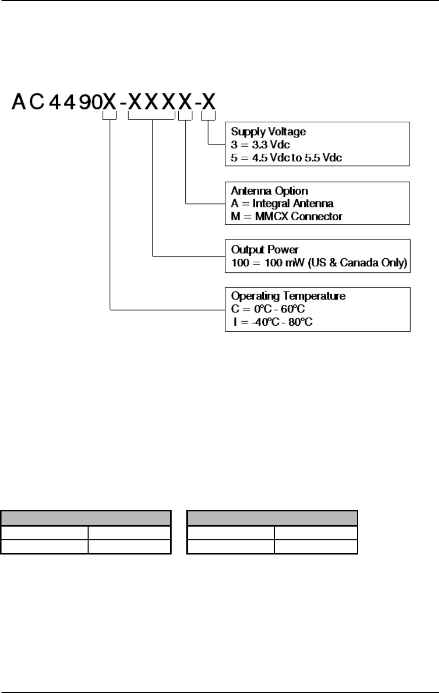
Ordering Information
Ordering Information Ordering Information
Ordering Information
2/18/03
2/18/032/18/03
2/18/03 36
3636
36
8.
8.8.
8. Ordering Information
Ordering InformationOrdering Information
Ordering Information
8.1
8.18.1
8.1 P
PP
PRODUCT
RODUCT RODUCT
RODUCT P
PP
PART
ART ART
ART N
NN
NUMBER
UMBER UMBER
UMBER T
TT
TREE
REEREE
REE
8.2
8.28.2
8.2 P
PP
PRODUCT
RODUCT RODUCT
RODUCT P
PP
PART
ART ART
ART N
NN
NUMBERS
UMBERSUMBERS
UMBERS
Order transceivers using the following part number tables:
3.3V, 100 mW Part Numbers 4.5 – 5.5V, 100 mW Part Numbers
AC4490C-100A-3 AC4490I-100A-3 AC4490C-100A-5 AC4490I-100A-5
AC4490C-100M-3 AC4490I-100M-3 AC4490C-100M-5 AC4490I-100M-5

Ordering Information
Ordering Information Ordering Information
Ordering Information
2/18/03
2/18/032/18/03
2/18/03 37
3737
37
8.3
8.38.3
8.3 D
DD
DEVELOPER
EVELOPER EVELOPER
EVELOPER K
KK
KIT
IT IT
IT P
PP
PART
ART ART
ART N
NN
NUMBERS
UMBERSUMBERS
UMBERS
Order Developer Kits using the following part number tables:
4.5 – 5.5V, 200 mW Developer Kit Part Numbers
SDK-AC4490I-100A-5
SDK-AC4490I-100M-5
All Developer Kits include (2) transceivers, (2) RS232 Serial Adapter Boards, (2) 6Vdc unregulated
power supplies, (2) Serial cables, (2) S467FL-6-RMM-915S dipole antennas with 6” pigtail and MMCX
connector, configuration/testing software, and integration engineering support.