Laird Connectivity APEX 802.15.4 Transceiver Module User Manual Manual
LS Research, LLC 802.15.4 Transceiver Module Manual
Manual

APEX/APEX LT
Datasheet (Preliminary Rev 0.2) www.lsr.com Page 1 of 20
APEX/APEX LT DATASHEET
ZigBee Ready Modules
1 Product Description
The LS Research APEX and APEX LT modules are 2.4 GHz 802.15.4 data transceivers
providing a cost-effective solution for data links and wireless networks.
The APEX module is based on the Ember EM250 802.15.4/Zigbee platform and supports
point to point, point to multi-point, and EmberZNet applications. It provides a true Zigbee
module combining an IEEE 802.15.4 compliant radio transceiver with a 16-bit microprocessor.
The APEX LT module is based on the Ember EM260 Zigbee network processor providing an
IEEE 802.15.4 compliant radio transceiver with a SPI based interface to an application
microprocessor, giving the flexibility to choose the external microprocessor size to best fit the
application.
Both APEX and APEX LT utilize a 100mW power amplifier, providing for enhanced range
performance over standard 802.15.4/Zigbee implementations. The APEX modules offer a
standard integrated PCB trace antenna. Alternatively, each module has the option to be
populated with a MMCX connector for use with an external cabled antenna.
The hardware design files can be licensed from LS Research or LS Research can modify the
hardware to accommodate specific application requirements. The APEX modules provide a
low cost, best in class performance, in a compact form factor.
APEX/APEX LT
Datasheet (Preliminary Rev 0.2) www.lsr.com Page 2 of 20
2 Key Features
• 100mW output
• Specifically designed for use with EmberZNet
• Small form factor (1.00” x 1.275”)
• Integrated antenna
• Supported connector for external antenna
• 16 RF channels (Channel 16 at a reduced power level)
• Long Range: over 4000 feet
• Output power software controlled 1mW – 100mW
• Integrated hardware support for Ember InSight Development Environment
• Non-intrusive debug interface (SIF)
• AES-128 encryption
• Constant RF output power over voltage range of 2.1 – 3.6V
• RoHS compliant
APEX module
• 128 kB Flash memory
• 5 kB SRAM
• 16-bit XAP2b microprocessor
• 16 GPIO connections
• Two serial controllers with DMA – SPI, I2C, UART functionality
• Integrated ADC with 12-bit resolution
APEX LT module
• Integrated IEEE 802.15.4 PHY and MAC
• Dedicated network processor
• SPI-slave or UART interface to application microcontroller
• Handles all processing and timing intensive tasks of Zigbee protocol
3 Absolute Maximum Ratings
Rating Value Unit
Power Supply Voltage 3.6 Vdc
Voltage on any digital pin VDD + 0.3,
Max 3.6
Vdc
RF Input Power +10 dBm
Storage Temperature Range -45 to 125 ºC
Note: Under no circumstances exceeding the maximum ratings in Table can be allowed. Such a stress may cause
permanent damage to the module or devices
APEX/APEX LT
Datasheet (Preliminary Rev 0.2) www.lsr.com Page 3 of 20
4 Operating Conditions
Characteristic Min Typ Max Unit
Power Supply Voltage (Vdd) 2.1 3.6 V
Input Frequency 2405 2480 MHz
Ambient Temperature Range -40 25 85 ºC
Logic Input Low Voltage 0 20% Vdd V
Logic Input High Voltage 80% Vdd Vdd V
5 Electrical Specifications
At 25ºC, Vdd = 3.3V for both APEX and APEX LT unless stated otherwise.
5.1 General
Parameter Min Typ Max Unit
RF Frequency Range 2400 2483.5 MHz
RF Data Rate 250 kbps
Microcontroller Operating Frequency (APEX only) 12 MHz
Flash Memory (APEX only) 128 kB
RAM (APEX only) 5 kB
5.2 Power Consumption
Parameter Min Typ Max Unit
Transmit Mode (100mW output)
APEX 170 mA
APEX LT 170 mA
Receive Mode
APEX 37 mA
APEX LT 37 mA
Standby Mode
10mW 5 µA
100mW 5 µA
Boost mode is an optional higher performance radio mode that is software selectable to boost receiver sensitivity.
5.3 Transmitter
Parameter Min Typ Max Unit
Nominal Output Power 20 dBm
Programmable Output Power range 32 dB
Error Vector Magnitude 15 35 %
APEX/APEX LT
Datasheet (Preliminary Rev 0.2) www.lsr.com Page 4 of 20
5.4 Receiver
Parameter Min Typ Max Unit
Receiver Sensitivity (1% PER) – normal mode -92 -96 dBm
Receiver Sensitivity (1% PER) – boost mode -93 -97 dBm
Saturation (Maximum Input Level) (1% PER) 0 dBm
802.15.4 Adjacent Channel Rejection
APEX 35 dB
APEX LT 30 dB
802.15.4 Alternate Channel Rejection 40 dB
802.11g Rejection (±10 MHz)
APEX 40 dB
APEX LT 30 dB
5.5 Control DC characteristics
Parameter Min Typ Max Unit
Logic Input Low 0 0.2VDD V
Logic Input High 0.8VDD VDD V
Logic Output Low 0 0.18VDD V
Logic Output High 0.82VDD VDD V
Output source current (standard pad – APEX) 4 mA
Output sink current (standard pad – APEX) 4 mA
Output source current (high current pad – APEX) 8 mA
Output sink current (high current pad – APEX) 8 mA
I/O pin pull-up and pull-down resistor (APEX) 30 kΩ
Please refer to the Ember EM250/EM260 datasheets (www.ember.com) for further information
or more details regarding the functional descriptions of the system modules.
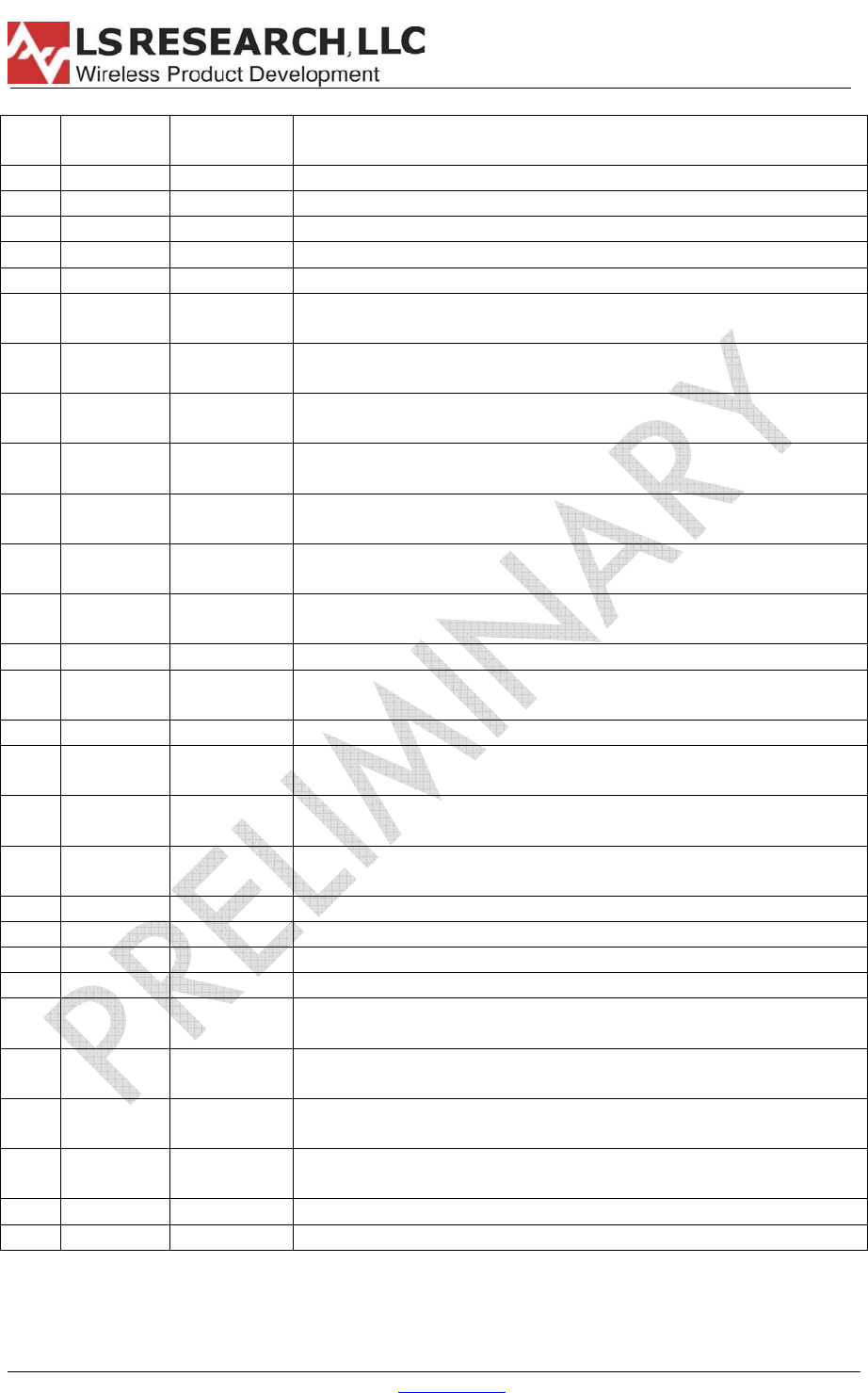
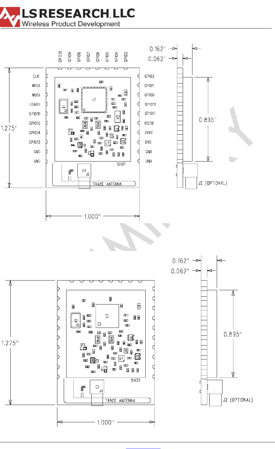
6 Pin Signals, I/O port configuration
The APEX/APEX LT modules have 28 edge I/O interfaces for connection to the user’s host
board. Figure 1 shows the layout of the 28 edge castellations.
Pin 10 Pin 19
Pin 28
Pin 1
Figure 1
APEX/APEX LT
Datasheet (Preliminary Rev 0.2) www.lsr.com Page 5 of 20
6.1 The I/O pin assignments for the APEX module
Pin
#
Name Type Description
1 GROUND GND Ground
2 GROUND GND Ground
3 GROUND GND Ground
4 VDD PI Power Supply Input
5 RSTB DI Reset, active low
6 GPIO11 DI/DO General Purpose Digital I/O, SC1 UART CTS, SC1 SPI master
clock, or Capture Input A of Timer 2
7 GPIO12 DI/DO General Purpose Digital I/O, SC1 UART RTS, or Capture
Input B of Timer 2
8 GPIO0 DI/DO General Purpose Digital I/O, SC2 SPI MOSI, or Capture
Input A of Timer 1
9 GPIO1 DI/DO General Purpose Digital I/O, SC2 SPI MISO, SC2 I2C SDA,
or Capture Input A of Timer 2
10 GPIO2 DI/DO General Purpose Digital I/O, SC2 SPI master clock, SC2 I2C
SCL, or Capture Input B of Timer 2
11 GPIO3 DI/DO General Purpose Digital I/O, SC2 SPI slave select, or
Capture Input B of Timer 1
12 GPIO4 DI/DO/AI General Purpose Digital I/O, ADC Input 0, or PTI frame
signal
13 GPIO5 DI/DO/AI General Purpose Digital I/O, ADC Input 1, or PTI data signal
14 GPIO6 DI/DO/AI General Purpose Digital I/O, ADC Input 2, Timer 2 Clock
Input, or Timer 1 Enable
15 GPIO7 DO Regulator Enable, active high (see section 8)
16 GPIO8 DI/DO/AO General Purpose Digital I/O, ADC Reference Output, Timer 1
Clock Input, Timer 2 Enable, or Source A Interrupt
17 GPIO9 DI/DO General Purpose Digital I/O, SC1 TXD, SC1 MO, SC1 I2C
Data, or Capture Input A of Timer 1
18 GPIO10 DI/DO General Purpose Digital I/O, SC1 RXD, SC1 MI, SC1 I2C
Clock, or Capture Input B of Timer 1
19 CLK DI SIF Interface clock
20 MISO DO SIF Interface master in/slave out
21 MOSI DI SIF Interface master out/slave in
22 LOADB DI/DO SIF Interface load strobe
23 GPIO16 DI/DO General Purpose Digital I/O, Output B of Timer 1, Capture
Input B of Timer 2, or Source D Interrupt
24 GPIO15 DI/DO General Purpose Digital I/O, Output A of Timer 1, Capture
Input A of Timer 2, or Source C Interrupt
25 GPIO14 DI/DO General Purpose Digital I/O, Output B of Timer 2, Capture
Input B of Timer 1, or Source B Interrupt
26 GPIO13 DI/DO General Purpose Digital I/O, Output A of Timer 2, or
Capture Input A of Timer 1
27 GROUND GND Ground
28 GROUND GND Ground
Unused I/O pins should be left unconnected and the pin state set via the Host Protocol.
DI = Digital Input PI = Power Input AI = Analog Input
DO = Digital Output GND = Ground AO = Analog Output

APEX/APEX LT
Datasheet (Preliminary Rev 0.2) www.lsr.com Page 6 of 20
The APEX module contains 16 GPIO ports that are shared with other peripheral or alternate
functions. The alternate functions can be utilized on a variety of different GPIOs as detailed
in the following table of pin assignments and definitions. All the GPIO pads are selectable as
input, output, or bi-directional and have an internal pull-up or pull-down.
The integrated Serial Controller SC1 can be configured for SPI (master-only), I2C (master-
only), or UART functionality. The Serial Controller SC2 can be configured for SPI (master or
slave) or I2C (master-only) operation. The integrated ADC can sample analog signals from
three GPIO pins single-ended or differentially. The integrated voltage reference VREF for
the ADC can be made available to a GPIO port.
Please consult the Ember EM250 datasheet for details on configuring and controlling the
information flow of the APEX module interface ports to setup the following:
• GPIO Data Registers
• Alternate function routing
• External Interrupts
• Serial Controller SC1 module (UART mode, SPI Master mode, I2C Master mode)
• Serial Controller SC2 module (SPI modes, I2C Master mode)
• General Purpose Timers
• ADC Module
• Event Manager
APEX/APEX LT
Datasheet (Preliminary Rev 0.2) www.lsr.com Page 7 of 20
6.2 I/O pin assignments for the APEX LT module
Pin # Name Type Description
1 GROUND GND Ground
2 GROUND GND Ground
3 GROUND GND Ground
4 GROUND GND Ground
5 VDD PI Power Supply Input
6 nRESET DI Reset, active low
7 MOSI DI SPI Data, Master Out/Slave In (from Host to APEX LT)
8 MISO DO SPI Data, Master In/Slave Out (from APEX LT to Host)
9 SCLK DI SPI Clock (from Host to APEX LT)
10 VPA_EN DI APEX LT Enable, active high (see section 8)
11 nRTS DO UART RTS
12 nSSEL_INT/nCTS DI SPI Slave Select (from Host to APEX LT)/UART CTS
13 PTI_EN DO PTI Frame signal
14 PTI_DATA DO PTI Data signal
15 TXD DO UART TXD
16 nHOST_INT/RXD DO/DI Host Interrupt Signal (from APEX LT to Host) or UART RXD
17 nWAKE DI Wake Interrupt Signal (from host to APEX LT)
18 GROUND GND Ground
19 SIF_CLK DI SIF Interface clock
20 SIF_MISO DO SIF Interface master in/slave out
21 SIF_MOSI DI SIF Interface master out/slave in
22 nSIF_LOAD DI/DO SIF Interface load strobe
23 SDBG DO Spare Debug Signal
24 LINK_ACTIVITY DO Link and Activity signal
25 GROUND GND Ground
26 GROUND GND Ground
27 GROUND GND Ground
28 GROUND GND Ground
Unused I/O pins should be left unconnected and the pin state set via the Host Protocol.
DI = Digital Input PI = Power Input AI = Analog Input
DO = Digital Output GND = Ground AO = Analog Output
The APEX LT module provides a connection to the Ember Serial API over the SPI allowing the
application development to be completed on a host microprocessor of choice. In addition to
the SPI signals, two additional signals (nHOST_INT and nWAKE) provide a handshake
mechanism. The module is the slave device with all transactions initiated by the host. Please
consult the EM260 datasheet (www.ember.com) for details on the SPI Protocol including:
• Physical Interface Configuration
• SPI Transactions
• SPI Protocol Timing Parameters & Waveforms
• Data Formatting
• SPI Commands & Responses
• Handling Resets and Power Cycling
• Transaction Examples
APEX/APEX LT
Datasheet (Preliminary Rev 0.2) www.lsr.com Page 8 of 20
7 SIF Interface
The APEX and APEX LT modules provide access to the SIF module programming and debug
interface. Consult the EM250 and EM260 datasheets for further details on the following
features it provides
• Production Testing
• Firmware Download
• Product Control and Characterization
• XAP2b Code Development (APEX only)
8 Power Amplifier Regulator Control Line
Both the APEX and APEX LT modules include a separate 1.8V regulator for the power
amplifier bias to enable the consistent module output performance over the wide Vdd voltage
range of 2.1 – 3.6 volts. To prevent excessive sleep currents, this regulator needs to be
disabled when the module is put into sleep mode. An external pull up resistor population
option is provided on each module (R6) to allow the regulator to be constantly enabled. This
option will increase the sleep current of the module well above the specified values.
The following table provides the specifications for the regulator enable control line.
GPIO7 (APEX), VPA_EN (APEX LT)
Parameter Min Typ Max Unit
Regulator enable voltage 0.95 V
Regulator disable voltage 0.4 V
Enable line current (VEN = 0) 0.1 µA
Enable line current (VEN = Vdd) 10 µA
Turn on Time 250 µsec
On the APEX LT module the VPA_EN control must be provided by the host microprocessor. In
normal operation, the VPA_EN line must be set high. It must be set low when the module is put
into sleep mode in conjunction with putting the EM260 into deep sleep. Upon a module wake-
up the Turn on time requirement of 250µsec must be met prior to any transmission to allow the
module regulator to settle. The EM260 wake up time is separate from this value as this
250µsec requirement applies only to the external power amplifier.
On the APEX module, the regulator control line is brought to the module ports via GPIO7. The
host can drive this port as on the APEX LT module, but alternatively, the EM250 can use the
default serial digital function of GPIO7 which is as an external voltage regulator enable.
Please consult the EM250 datasheet for details on the operation of this function. Note that
both approaches preclude the use of the GPIO7 port for any other possible functions
including the use as the ADC3 input.
If the application does not put the module to sleep or if sleep current is not an issue, the
power amplifier regulator may be permanently enabled by tying the control line high. In this
setup, the sleep current will increase by 80µA over the value provided in section 5.2.

APEX/APEX LT
Datasheet (Preliminary Rev 0.2) www.lsr.com Page 9 of 20
9 Antenna
The APEX and APEX LT modules include an integrated PCB trace antenna. An optional
configuration with a MMCX connector is also available. This will enable connector to a 50-
ohm external antenna of the user’s choice.
The integrated PCB antenna topology is an F-antenna. This antenna is used because it is
reasonably compact, has a fairly omni-directional radiation pattern, good efficiency, and is
very simple. An adequate ground plane is necessary to provide good efficiency. The ground
plane of the host board on which the module is mounted increases the effective antenna
ground plane size and improves the antenna performance if done per the guidelines provided
in this datasheet.
The antenna radiation patterns are dependent upon the host board the APEX/APEX LT module
is mounted on. Measured radiation patterns of the module alone are available by contacting
LS Research.
The environment the module is placed in will dictate the range performance. The non-ideal
characteristics of the transmission channel result in the transmitted signal producing reflection,
diffraction, and/or scattering. All of these factors randomly combine to create extremely
complex scenarios.
It is also best to keep some clearance between the antenna and nearby objects. This includes
how the module is mounted in the product enclosure. Unless the items on the following list of
recommendations are met, the radiation pattern can be heavily distorted.
• Never place ground plane or copper trace routing underneath the antenna.
• Never place the antenna very close to metallic objects.
• In the final product, ensure that any wiring or other components do not get too close to
the antenna.
• The antenna will need a reasonable ground plane area on the mother board area to
be efficient.
• Do not use a metallic enclosure or metallized plastic for the antenna.
• Try to keep any plastic enclosure greater than 1 cm from the antenna in any
orientation.
APEX/APEX LT
Datasheet (Preliminary Rev 0.2) www.lsr.com Page 10 of 20
10 Mechanical Drawing – APEX
APEX LT
APEX/APEX LT
Datasheet (Preliminary Rev 0.2) www.lsr.com Page 11 of 20
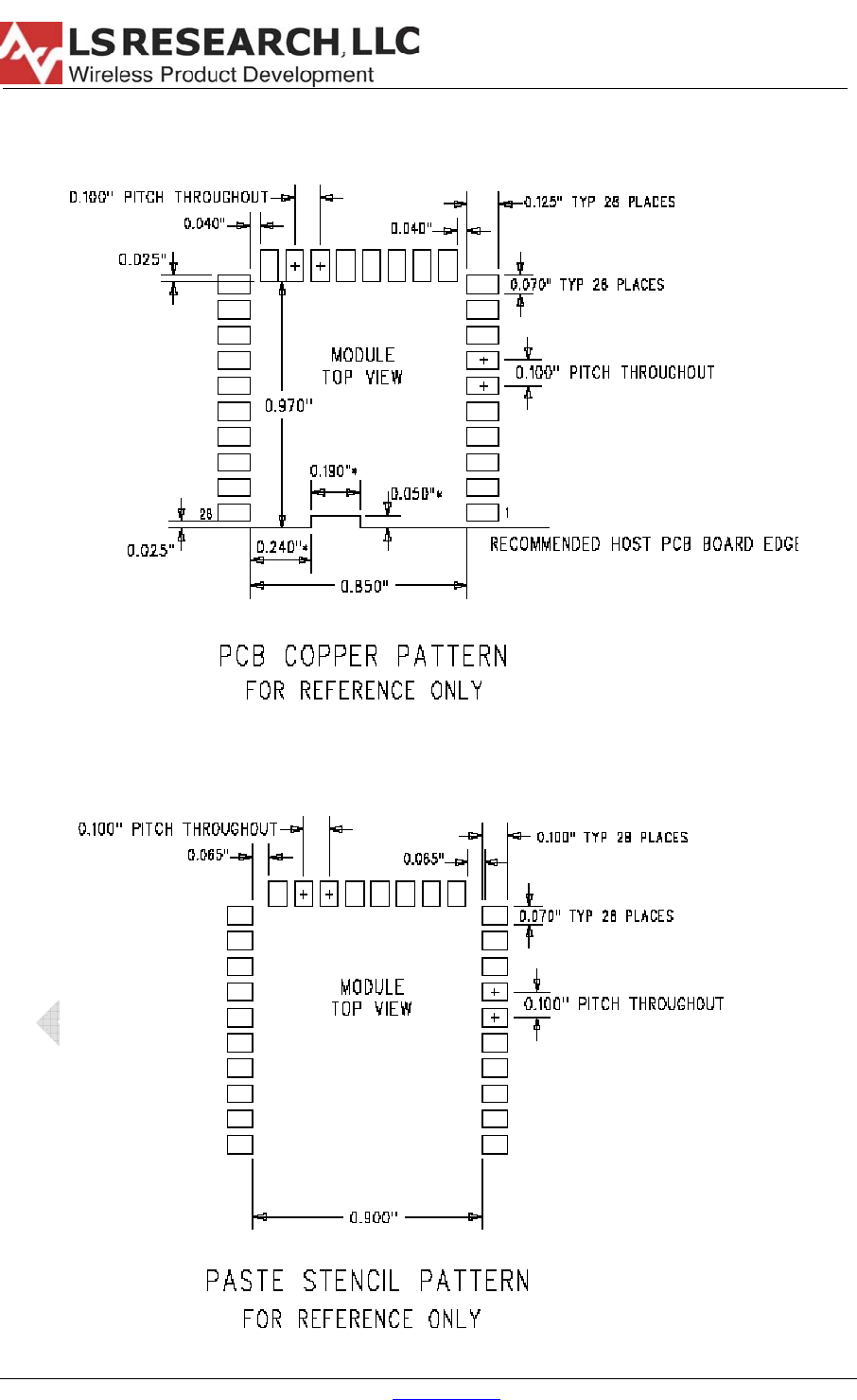
11 Mounting considerations
PCB Pattern Layout
For both APEX/APEX LT
APEX/APEX LT
Datasheet (Preliminary Rev 0.2) www.lsr.com Page 12 of 20
Keep out areas
APEX/APEX LT
The footprint recommends the APEX/APEX LT module is to be mounted so the antenna is
overhanging the board edge. This will provide the best antenna performance for the PCB
trace antenna. It is also recommended to have a ground plane on the host board underneath
the rest of the module, up to the recommended PCB edge. This will only improve the antenna
performance by increasing the overall ground plane.
Traces can be run underneath the module on the host PCB as long a there is an uninterrupted
ground plane on one layer as well. LS Research will provide any guidance and help with the
host PCB layout.

APEX/APEX LT
Datasheet (Preliminary Rev 0.2) www.lsr.com Page 13 of 20
12 Agency Certifications
FCC Part 15.247 Module Certified (Mobile)
The APEX and APEX LT modules comply with Part 15 of the Federal Communications
Commission rules and regulations. To meet the FCC Certification requirements, the user must
meet these regulations.
• The text on the FCC ID label provided with the module is placed on the outside of the
final product.
• The modules may only use the antennas that have been tested and approved with this
module.
o The on-board PCB trace antenna
o Nearson S131CL-5-RMM-2450S antenna.
To meet the section 15.209 emission requirements in the restricted frequency bands of section
15.205, the maximum transceiver transmitter power setting for both the APEX (EM250) and
APEX LT (EM260) modules vary depending on the channel used within the band of operation
as follows:
APEX module using external antenna – maximum channel power setting
Channel 11 (2405 MHz) -4
Channel 12 (2410 MHz) – Channel 23 (2465 MHz) 3
Channel 24 (2470 MHz) -7
Channel 25 (2475 MHz) -14
Channel 26 (2480 MHz) -2b
APEX module using on board PCB trace antenna – maximum channel power setting
Channel 11 (2405 MHz) – Channel 24 (2470 MHz) 3
Channel 25 (2475 MHz) -12
Channel 26 (2480 MHz) -2b
APEX LT module using either external or PCB trace antenna – maximum channel power
setting
Channel 11 (2405 MHz) – Channel 24 (2470 MHz) 0
Channel 25 (2475 MHz) -10
Channel 26 (2480 MHz) -26
Per section 2.109, the APEX and APEX LT modules have been certified by the FCC for use with
other products without additional certification. Any modifications to this product may violate
the rules of the Federal Communications Commission and make operation of the product
unlawful.
Per sections 15.107 and 15.109, the user’s end product must be tested to comply with
unintentional radiators for compliance.
Per Section 47 C.F.R. Sec.15.105(b), the APEX and APEX LT modules are certified as a mobile
device for the FCC radiation exposure limits set forth for an uncontrolled environment. The
antenna used with this module must be installed to provide a separation distance of at least 8
inches (20cm) from all persons. If the module is to be used in a handheld application, the user
APEX/APEX LT
Datasheet (Preliminary Rev 0.2) www.lsr.com Page 14 of 20
is responsible for passing the additional FCC part 2.1093 rules (SAR) and FCC Guidelines for
Human Exposure to Radio Frequency Electromagnetic Fields, OET Bulletin and Supplement C.
The labeling requirements for Industry Canada are similar to those of the FCC. A visible label
on the outside of the final product must display the IC labeling. The user is responsible for the
end product to comply with IC ICES-003 (Unintentional radiators).
The APEX and APEX LT modules have been certified per EN 300-328-1 for use in European
countries. The user must ensure compliance of any final product to the European harmonized
EMC and safety standards. Annex II of the R&TTE Directive gives the requirements for the
issuance of a Declaration of Conformity.
The CE marking must be affixed legibly and indelibly to a visible location on the user’s
product.
To meet the EN 300-328-1 power spectral density requirements of Clause 4.3.2.2, the
maximum transceiver power setting for the APEX module and the APEX LT module are as
follows:
Maximum transceiver power setting for APEX CE approval
Channel 11 (2405 MHz) - Channel 22 (2460 MHz) -15
Channel 23 (2465 MHz) – Channel 26 (2480 MHz) -20
Maximum transceiver power setting for APEX LT CE approval
TBD
12.1 FCC approved antennas
Integrated PCB trace antenna
Nearson S131CL-5-RMM-2450S
A 2.4GHz Dipole antenna with a 5 inch cable and a right angle MMCX
connector.

APEX/APEX LT
Datasheet (Preliminary Rev 0.2) www.lsr.com Page 15 of 20
13 Shipment, Handling, and Storage
13.1 Shipment
The LS Research APEX Modules are delivered in single piece, or 50 piece cartons in individual
anti-static bags.
13.2 Handling
The APEX/APEX LT Module is designed and packaged to be processed in an automated
assembly line.
! Warning - The Modules contain highly sensitive electronic circuitry. Handling without proper
ESD protection may destroy or damage the module permanently.
! Warning - According to JEDEC ISP, the APEX Modules are moisture sensitive devices.
Appropriate handling instructions and precautions are summarized in Section 2.1. Read
carefully to prevent permanent damages due to moisture intake.
13.3 Storage
Storage/Shelf life in sealed bags is 12 months at <40ºC and <90% relative humidity.
14 Processing
14.1 Moisture Preconditioning
Both substrate and some components can absorb moisture. JEDEC specification J-STD-020 must
be observed to prevent the delamination and cracking associated with the “popcorn” effect”
during solder reflow, (the popcorn effect can be described as miniature explosions of water
vapor that has been trapped in gaps).
Baking before processing is required if module is exposed to excessive humidity.
Recommended baking procedure:
Oven: Convection flow oven.
Duration: 48 hours
Temperature: 125ºC
Humidity: Below 5%.
After conditioning (baking) modules should be processed within the specified floor life:
for products with moisture sensitivity level 4, the floor life is three days, or precisely 72 hours,
assuming factory temperature and humidity conditions of <30ºC, and <60% relative
humidity.
If they cannot be processed within this time period, place the modules with desiccant and a
moisture indicator into a humidity proof bag and use a vacuum hot barrier sealing machine
for sealing
Other Storage options such as a nitrogen cabinet or dry box are also possible.
Note: A repeated baking process will reduce the wetting effectiveness of the land contacts.

APEX/APEX LT
Datasheet (Preliminary Rev 0.2) www.lsr.com Page 16 of 20
14.2 Reflow Soldering
A convection soldering oven is recommended over the infrared radiation type oven.
Convection ovens allow more precise temperature control, and more even heating of parts
regardless of material composition, thickness, or color.
Consider the IPC-7530 Guidelines for temperature profiling for mass soldering processes,
reflow and wave, published 2001.
14.2.1 Preheat Phase
Initial heating of component leads and solder paste balls, for removal of residual humidity.
Note: the preheat phase is not intended to replace prior baking procedures.
• Temperature rise rate: 1-4ºC/sec
Note: excessive slumping can result if the temperature rise is too rapid.
• Time: 60-120 seconds
Note: If the preheat is insufficient, large solder balls tend to be generated. Conversely, if
preheat is excessive, small and large balls will be generated in clusters.
• End Temperature: 150-200ºC
14.2.2 Heating/Reflow Phase
The temperature rises above the liquidus temperature of the solder paste selected. Avoid a
sudden rise in temperature as any slump of the solder paste could become worse.
• Limit time above liquidus temperature to 20-40 seconds.
• Peak reflow temperature: 230-250ºC
14.2.3 Cooling Phase
A controlled cooling phase avoids unwanted metallurgical effects of the solder, and possible
mechanical tensions in the products. Controlled cooling helps achieve the brightest possible
solder fillets with a good shape and low contact angle.
• Temperature fall rate: max 3ºC/sec
14.3 Pb-free Soldering Paste
Use of “No Clean” soldering paste is strongly recommended, as it does not require cleaning
after the soldering process. The pastes listed in the examples below meet these criteria.
14.3.1 Soldering Paste: Indium 5.1 (Indium Corporation of America)
Alloy Specification: SAC305 - Sn Zinc 96.5%/Ag Silver 3.0%/Cu Copper 0.5%
Alloy Specification: SAC387 - Sn Zinc 95.5%/Ag Silver 3.8%/Cu Copper 0.7%
Melting Temperature: 217ºC
14.3.2 Soldering Paste: LFSOLDER TLF-206-93F (Tamura Kaken [UK] Ltd.)
Alloy Specification: Sn Zinc 95.5%/Ag Silver 3.9%/Cu Copper 0.6%
Melting Temperature: 216-221ºC

APEX/APEX LT
Datasheet (Preliminary Rev 0.2) www.lsr.com Page 17 of 20
The final choice of the soldering paste depends on individual factory approved manufacturing
procedures.
Stencil Thickness: 150 µm for host boards
Note: The quality of the solder joints on the castellations (‘half vias’) where they contact the
host board should meet the appropriate IPC specification. See IPC-A-610-12.2.4.
14.4 Cleaning
In general, cleaning the populated modules is strongly discouraged. Residuals under the
module cannot be easily removed with any cleaning process.
• Cleaning with water can lead to capillary effects where water is absorbed into the gap
between the host board and the module. The combination of soldering flux residuals and
encapsulated water could lead to short circuits between neighboring pads. Water could also
damage any stickers or labels.
• Cleaning with alcohol or a similar organic solvent will likely flood soldering flux residuals
into the two housings, which is not accessible for post-washing inspection. The solvent could also
damage any stickers or labels.
• Ultrasonic cleaning could damage the module permanently.
The best approach is to consider using a “no clean” soldering paste and eliminate the post
soldering cleaning step.
14.5 Optical Inspection
After soldering the Module to the host board, consider optical inspection to check the
following:
• Proper alignment and centering of the module over the pads.
• Proper solder joints on all pads.
• Excessive solder or contacts to neighboring pads, or vias.
14.6 Repeating Reflow Soldering
Only a single reflow soldering process is encouraged for host boards.
14.7 Wave Soldering
If a wave soldering process is required on the host boards due to the presents of leaded
components, only a single wave soldering process is encouraged.
14.8 Hand Soldering
Hand soldering is possible. Use a soldering iron temperature setting equivalent to 350ºC,
follow IPC recommendations/reference document IPC-7711.
APEX/APEX LT
Datasheet (Preliminary Rev 0.2) www.lsr.com Page 18 of 20
14.9 Rework
The APEX & APEX LT Module can be unsoldered from the host board. Use of a hot air re-work
tool and hot plate for pre-heating from underneath is recommended. Avoid overheating.
! Warning - Never attempt a rework on the module itself, e.g. replacing individual
components. Such actions will terminate warranty coverage.
14.10 Additional grounding
Attempts to improve module or system grounding by soldering braids, wires, or cables onto
the module RF shield cover is done at the customers own risk. The numerous ground pins at the
module perimeter should be sufficient for optimum immunity to external RF interference.
14.11 Conformal Coating
Conformal coating may be necessary in certain applications. Please note that the RF shield
and the sticker prevent optimum inflow of liquids or aerosols.
15 Contact Info
For more information e-mail
sales@lsr.com
16 Document history
Revision 0.0 (1-29-2007) Preliminary release
Revision 0.1 (6-1-2007) Updated for performance, APEX LT pin out, mounting considerations.
Revision 0.2 (1-22-2008) Updated for FCC/CE power levels, added section 18
17 Disclaimer
LS Research, LLC believes the information in this document is correct and accurate at the time
of release. However, LS Research, LLC reserves the right to make changes to this product
without notice.
18 Statements
Compliance Statement (Part 15.19)
This device complies with Part 15 of the FCC Rules.
Operation is subject to the following two conditions:
1. This device may not cause harmful interference, and
2. This device must accept any interference received,

APEX/APEX LT
Datasheet (Preliminary Rev 0.2) www.lsr.com Page 19 of 20
including interference that may cause undesired operation.
Warning (Part 15.21)
Changes or modifications not expressly approved by the party
responsible for compliance could void the user’s authority to
operate the equipment.
FCC Interference Statement (Part 15.105 (b))
This equipment has been tested and found to comply with the limits for a Class B digital
device, pursuant to Part 15 of the FCC Rules. These limits are designed to provide reasonable
protection against harmful interference in a residential installation. This equipment generates
uses and can radiate radio frequency energy and, if not installed and used in accordance
with the instructions, may cause harmful interference to radio communications. However, there
is no guarantee that interference will not occur in a particular installation. If this equipment
does cause harmful interference to radio or television reception, which can be determined by
turning the equipment off and on, the user is encouraged to try to correct the interference by
one of the following measures:
- Reorient or relocate the receiving antenna.
- Increase the separation between the equipment and receiver.
- Connect the equipment into an outlet on a circuit different from that
to which the receiver is connected.
- Consult the dealer or an experienced radio/TV technician for help.
RF Exposure (OET Bulletin 65)
To comply with FCC’s RF exposure limits for general population / uncontrolled exposure, the
antenna(s) used for this transmitter must be installed to provide a separation distance of at
least 20 cm from all persons and must not be co-located or operating in conjunction with any
other antenna or transmitter.
OEM Responsibility to the FCC Rules and Regulations
The APEX Module has been certified per FCC Part 15 rules for integration into products without
further testing or certification. To fulfill the FCC certification requirements the OEM of the APEX
Module must ensure that the information provided on the APEX Label is placed on the outside of the
final product.
The APEX Module is labeled with its own FCC ID Number. If the FCC ID is not visible when the
module is installed inside another device, then the outside of the device into which the module is
installed must also display a label referring to the enclosed module. This exterior label can use
wording such as the following:
“Contains Transmitter Module FCC ID: TFB-APEX”
or
“Contains FCC ID: TFB-APEX”
The OEM of the APEX Module must only use the approved antenna, which has been certified with
this module.
The OEM of the APEX Module must test their final product configuration to comply with Unintentional
Radiator Limits before declaring FCC compliance per Part 15 of the FCC rules.
APEX/APEX LT
Datasheet (Preliminary Rev 0.2) www.lsr.com Page 20 of 20
Industry Canada Statement per Section 4.0 of RSP-100
The term "IC:" before the certification / registration number only signifies that the Industry
Canada technical specifications were met.
Section 7.1.5 of RSS-GEN
Operation is subject to the following two conditions:
1) This device may not cause harmful interference, and
2) This device must accept any interference received,
including interference that may cause undesired operation.
Section 7.1.4 of RSS-GEN
This device has been designed to operate with the antenna(s) listed below, and having a
maximum gain of 2.0 dB. Antennas not included in this list or having a gain greater than 2.0
dB are strictly prohibited for use with this device. The required antenna impedance is 50
ohms.
List of all Antennas Acceptable for use with the Transmitter
Integrated PCB trace antenna
Nearson S131CL-5-RMM-2450S
Section 7.1.5 of RSS-GEN
To reduce potential radio interference to other users, the antenna type and its gain should be
so chosen that the equivalent isotropically radiated power (e.i.r.p.) is not more than that
permitted for successful communication.