Laird Connectivity BL652 Bluetooth 4.2 module (BLE only) User Manual
Laird Technologies Bluetooth 4.2 module (BLE only) Users Manual
Contents
- 1. Users Manual
- 2. CS-RegulatoryInfo-BL652 v1_6
Users Manual

A
Datasheet
BL652-SA and BL652-SC
Version 1.1

BL652
Datasheet
Embedded Wireless Solutions Support Center:
http://ews-support.lairdtech.com
www.lairdtech.com/bluetooth
2
© Copyright 2016 Laird. All Rights Reserved
Americas: +1-800-492-2320
Europe: +44-1628-858-940
Hong Kong: +852 2923 0610
REVISION HISTORY
Version
Date
Notes
Approver
1.0
20 July 2016
Initial Release
Jonathan Kaye
1.1
30 Aug 2016
Corrected Operating Temperature voltage to read
VCC 1.8 V-3.6 V rather than 1.7 V-3.6V
Corrected minor formatting issues and typo
Changed the SIO_02 pin # (OTA mode table) to 23 vs. 21
Raj Khatri
BL652
Datasheet
Embedded Wireless Solutions Support Center:
http://ews-support.lairdtech.com
www.lairdtech.com/bluetooth
3
© Copyright 2016 Laird. All Rights Reserved
Americas: +1-800-492-2320
Europe: +44-1628-858-940
Hong Kong: +852 2923 0610
CONTENTS
1 Overview and Key Features ................................................................................................................................. 4
2 Specification ......................................................................................................................................................... 5
3 Hardware Specifications ...................................................................................................................................... 9
4 Power Consumption .......................................................................................................................................... 19
5 Functional Description ....................................................................................................................................... 34
Power Management (includes Brown-out and Power on Reset) ......................................................... 34
Clocks and Timers ................................................................................................................................. 35
Memory for smartBASIC Application Code .......................................................................................... 35
Radio Frequency (RF) ............................................................................................................................ 35
NFC ........................................................................................................................................................ 35
UART Interface ...................................................................................................................................... 36
SPI Bus ................................................................................................................................................... 37
I2C Interface.......................................................................................................................................... 37
General Purpose I/O, ADC, PWM and FREQ ......................................................................................... 38
nRESET pin ............................................................................................................................................ 39
nAutoRUN pin ....................................................................................................................................... 39
vSP Command Mode ............................................................................................................................ 39
Two-wire Interface JTAG ...................................................................................................................... 40
BL652 Wakeup ...................................................................................................................................... 42
Low Power Modes ................................................................................................................................ 42
Temperature Sensor ............................................................................................................................. 42
Random Number Generator ................................................................................................................. 42
AES Encryption/Decryption .................................................................................................................. 42
Optional External Serial (SPI) Flash ....................................................................................................... 43
Optional External 32.768 kHz crystal.................................................................................................... 43
BL652-SA On-board Chip Antenna Characteristics ............................................................................... 45
6 Hardware Integration Suggestions .................................................................................................................... 46
Circuit .................................................................................................................................................... 46
PCB Layout on Host PCB - General ....................................................................................................... 48
PCB Layout on Host PCB for BL652-SA ................................................................................................. 48
External Antenna Integration with BL652-SC ....................................................................................... 50
7 Mechanical Details ............................................................................................................................................. 51
8 Application Note for Surface Mount Modules .................................................................................................. 53
Introduction .......................................................................................................................................... 53
Shipping ................................................................................................................................................ 53
Reflow Parameters ............................................................................................................................... 55
9 FCC and IC Regulatory Statements .................................................................................................................... 58
10 Japan (MIC) Regulatory ...................................................................................................................................... 62
11 CE Regulatory ..................................................................................................................................................... 63
12 EU Declarations of Conformity .......................................................................................................................... 64
13 Ordering Information ......................................................................................................................................... 65
14 Bluetooth SIG Qualification ............................................................................................................................... 65
BL652
Datasheet
Embedded Wireless Solutions Support Center:
http://ews-support.lairdtech.com
www.lairdtech.com/bluetooth
4
© Copyright 2016 Laird. All Rights Reserved
Americas: +1-800-492-2320
Europe: +44-1628-858-940
Hong Kong: +852 2923 0610
1 OVERVIEW AND KEY FEATURES
Every BL652 Series module is designed to enable OEMs to add single-mode Bluetooth Low Energy (BLE) v4.2 to
small, portable, power-conscious devices. The BL652 modules are supported with Laird’s smartBASIC, an event-
driven programming language that enables OEMs to make their BLE product development quicker and simpler,
significantly reducing time to market. smartBASIC enables customers to develop a complete embedded application
inside the compact BL652 hardware, connecting to a wide array of external sensors via its I2C, SPI, UART, ADC or
GPIO interfaces. The BL652 also provides flexibility in the OEM’s application development choice with full support
for using Nordic’s SDK and firmware tools.
Based on the world-leading Nordic Semiconductor nRF52832 chipset, the BL652 modules provide ultra-low power
consumption with outstanding wireless range via 4 dBm of transmit power. A broad range of BLE profiles including
Temperature and Heart Rate are available, and smartBASIC provides the ideal mechanism to support any BLE
profile development of your choice. This document should be read in conjunction with the smartBASIC user
manual.
Note: BL652 hardware is functionally capable as the nRF52832 chipset used in the module design.
Not all features are currently exposed within Laird’s smartBASIC firmware implementation.
Features and Benefits
Bluetooth v4.2 - Single mode
NFC-A Listen mode compliant
External or internal antennas
smartBASIC programming language or Nordic SDK
Compact footprint
Programmable Tx power +4 dBm to -20 dBm
Tx whisper mode (-40 dBm)
Rx sensitivity: -96 dBm
Ultra-low power consumption
Tx: 5.3 mA peak (at 0 dBm, DCDC on) – See Power
Consumption section Note 1
Rx: 5.4 mA peak (DCDC on) – See Power
Consumption section Note 1
Standby Doze: 1.2 uA typical
Deep Sleep: 0.4 uA – See Power Consumption
section Note 4
UART, GPIO, ADC, PWM, FREQ output, timers,
I2C, and SPI interfaces
Fast time-to-market
FCC, CE, IC, and Japan certified; Full Bluetooth
Declaration ID
Other regulatory certifications on request (all
certifications are in process)
No external components required
Industrial temperature range (-40 to + 85)
Application Areas
Medical devices
Wellness devices
iOS “appcessories”
Fitness sensors
Location awareness
Home automation
Note: Figures on this page are gathered from the nRF52 datasheet provided by Nordic.
BL652
Datasheet
Embedded Wireless Solutions Support Center:
http://ews-support.lairdtech.com
www.lairdtech.com/bluetooth
5
© Copyright 2016 Laird. All Rights Reserved
Americas: +1-800-492-2320
Europe: +44-1628-858-940
Hong Kong: +852 2923 0610
2 SPECIFICATION
Specification Summary
Table 1: BL652 Specifications
Categories
Feature
Implementation
Wireless
Specification
Bluetooth®
V4.2 – Single mode
Concurrent master and slave
Diffie-Hellman based pairing
Frequency
2.402 - 2.480 GHz
Maximum Transmit Power Setting
+4 dBm
Conducted BL652-SA
+4 dBm
Conducted BL652-SC
Minimum Transmit Power Setting
-20 dBm (in 4 dB steps) with smartBASIC command
-16 dBm, -12 dBm, - 8 dBm, - 4 dBm, 0 dBm
Tx Whisper Mode 1
Transmit Power
-40 dBm (min.) with smartBASIC command
Receive Sensitivity (0.1% BER)
-96 dBm typical
Link Budget
100 dB (@ 1 Mbps)
Range
Up to 100 meters in free space
Tx Whisper Modes
Range reduction feature with Tx Whisper modes via
smartBASIC command
Range
(Tx Whisper Mode 1)
<~100 cm
Raw Data Rates
1 Mbps (over-the-air)
NFC
NFC-A Listen mode compliant
Based on NFC forum specification
13.56 MHz
Date rate 106 kbps
NFC-A tag
– Can only be a target/tag; cannot be an
initiator
Modes of Operation:
Disable
Sense
Activated
Use Cases:
Touch-to-Pair with NFC
NFC enabled Out-of-Band Pairing
System Wake-On-Field function
Proximity Detection
Host Interface
and Peripherals
Total
32 x Multifunction I/O lines
UART
Tx, Rx, CTS, RTS
DCD, RI, DTR, DSR (See Note 1)
Default 115200,n,8,1
From 1,200bps to 1Mbps
BL652
Datasheet
Embedded Wireless Solutions Support Center:
http://ews-support.lairdtech.com
www.lairdtech.com/bluetooth
6
© Copyright 2016 Laird. All Rights Reserved
Americas: +1-800-492-2320
Europe: +44-1628-858-940
Hong Kong: +852 2923 0610
Categories
Feature
Implementation
GPIO
Up to 32, with configurable:
I/O direction,
O/P drive strength (standard 0.5 mA or high 3mA/5
mA),
Pull-up /pull-down
ADC
Eight 8/10/12-bit channels
0.6 V internal reference
Configurable 4, 2, 1, 1/2, 1/3, 1/4, 1/5 1/6(default)
pre-scaling
Configurable acquisition time 3uS, 5uS,
10uS(default), 15uS, 20uS, 40uS.
One-shot mode
PWM output
PWM outputs on 12 GPIO output pins.
PWM output duty cycle: 0%-100%
PWM output frequency: Up to 500kHz
(See Note 7)
FREQ output
FREQ outputs on 2 GPIO output pins.
FREQ output frequency: 0 MHz-4MHz (50% duty
cycle)
I2C
One I2C interface (up to 400 kbps) (See Note 2)
SPI
One SPI Master interface (up to 4 Mbps)
(See Note 3)
Optional
External to the
BL652 module
External 32.768kHz crystal
For customer use, connect +/-20ppm accuracy
crystal for more accurate protocol timing.
External SPI serial flash
For customer use e.g. data-logging
Profiles
Services supported
(See Note 4)
Laird’s smartBASIC firmware supports the
following::
Central Mode
Peripheral Mode
Custom Series
Nordic SDK v3x0
Any exposed within the related Nordic softdevice
(application development to be done by OEM)
FW upgrade
smartBASIC runtime engine FW
upgrade (See Note 4)
Via JTAG or UART
Programmability
smartBASIC
On-board programming language similar to BASIC.
smartBASIC application download
Via UART
Via Over-the-Air (if SIO_02 pin is pulled high
externally)
Nordic SDK
Via JTAG
Control Protocols
Any
User defined via smartBASIC
BL652
Datasheet
Embedded Wireless Solutions Support Center:
http://ews-support.lairdtech.com
www.lairdtech.com/bluetooth
7
© Copyright 2016 Laird. All Rights Reserved
Americas: +1-800-492-2320
Europe: +44-1628-858-940
Hong Kong: +852 2923 0610
Categories
Feature
Implementation
Operating Modes
Self-contained Run mode
Selected by nAutoRun pin status: LOW (0V).
Then runs $autorun$ (smartBASIC application
script) if it exists.
Interactive/Development mode
HIGH (VCC).
Then runs via at+run (and file name of smartBASIC
application script).
Supply Voltage
Supply (VCC)
1.8- 3.6 V – Internal DCDC converter or LDO
(See Note 5)
Power
Consumption
(See Note 5)
Active Modes Peak Current (for
maximum Tx power +4 dBm)
– Radio only
Advertising mode
7.5 mA peak Tx (with DCDC)
Connecting mode
5.4 mA peak Tx (with DCDC)
Active Modes Peak Current (for
Tx Whisper mode2 power -40
dBm) – Radio only
Advertising mode
2.7 mA peak Tx (with DCDC)
Connecting mode
5.4 mA peak Tx (with DCDC)
Active Modes Average Current
Depends on many factors, see Power Consumption.
Ultra Low Power Modes
Standby Doze
Deep Sleep
1.2 uA typical (Note 6)
400 nA (Note 6)
Antenna Options
Internal
Ceramic chip monopole antenna – on-board
BL652-SA variant
External
Dipole antenna (with IPEX connector)
Dipole PCB antenna (with IPEX connector)
Connection via IPEX MH4 – BL652-SC variant
See the Antenna Information sections for FCC and
IC, MIC, and CE.
Physical
Dimensions
14 mm x 10 mm x 2.1 (TBC) mm
Pad Pitch: 0.75 mm
Pad Type: Plated half-moon edge pads (easy to
hand solder)
Weight
<1 gram
Environmental
Operating
-40 ˚C to +85 ˚C (VCC 1.8V-3.6V)
Storage
-40 ˚C to +85 ˚C
Miscellaneous
Lead Free
Lead-free and RoHS compliant
Warranty
Five-year Limited Lifetime
Development
Tools
Development Kit
Development kit (DVK-BL652-xx) and free software
tools
Approvals
Bluetooth®
Full Bluetooth SIG Declaration ID
FCC / IC / CE / MIC
All BL652 Series
Module Specification Notes:
Note 1
DSR, DTR, RI, and DCD can be implemented in the smartBASIC application.

BL652
Datasheet
Embedded Wireless Solutions Support Center:
http://ews-support.lairdtech.com
www.lairdtech.com/bluetooth
8
© Copyright 2016 Laird. All Rights Reserved
Americas: +1-800-492-2320
Europe: +44-1628-858-940
Hong Kong: +852 2923 0610
Module Specification Notes:
Note 2
With I2C interface selected, pull-up resistors on I2C SDA and I2C SCL must be connected externally as
per I2C standard.
Note 3
SPI interface (master) consists of SPI MOSI, SPI MISO, and SPI CLK. SPI CS is created by using any
spare SIO pin within the smartBASIC application script allowing multi-dropping.
Note 4
The BL652 module comes loaded with smartBASIC runtime engine firmware but does not come
loaded with any smartBASIC application script (as that is dependent on customer-end application or
use). Laird provides many sample smartBASIC application scripts covering the services listed.
Additional BLE services are being added every quarter.
Note 5
Use of the internal DCDC convertor or LDO is decided by the underlying BLE stack.
Note 6
These figures are measured on the BL652-Sx-xx.
Deep Sleep current for BL652-Sx-xx ~400nA (typical)
Standby Doze current for BL652-xx-A1 1.2uA (typical)
Note 7
PWM output signal has a frequency and duty cycle property. PWM output is generated using
dedicated hardware in the chipset. There is a trade-off between PWM output frequency and
resolution.
For example:
PWM output frequency of 500 kHz (2 uS) results in resolution of 1:2.
PWM output frequency of 100 kHz (10 uS) results in resolution of 1:10.
PWM output frequency of 10 kHz (100 uS) results in resolution of 1:100.
PWM output frequency of 1 kHz (1000 uS) results in resolution of 1:1000.
Refer to the smartBASIC user guide for details. It’s available from the Laird BL652 product page.
BL652
Datasheet
Embedded Wireless Solutions Support Center:
http://ews-support.lairdtech.com
www.lairdtech.com/bluetooth
9
© Copyright 2016 Laird. All Rights Reserved
Americas: +1-800-492-2320
Europe: +44-1628-858-940
Hong Kong: +852 2923 0610
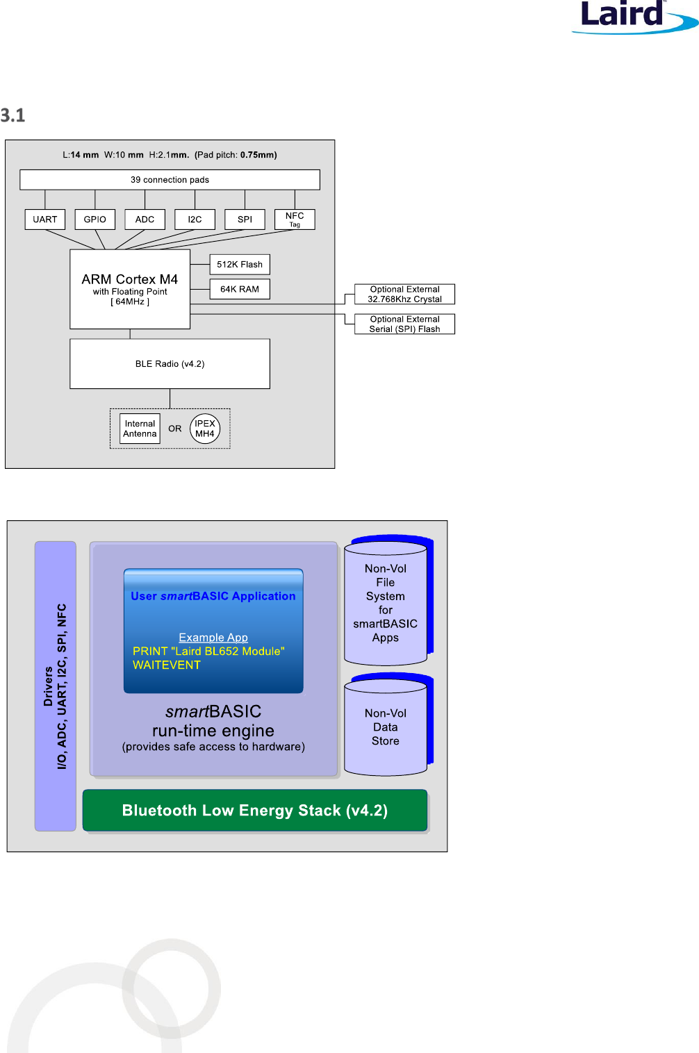
3 HARDWARE SPECIFICATIONS
Block Diagram and Pin-out
Figure 1: BL652 Block diagram
Figure 2: Functional HW and SW block diagram for BL652 series BLE smartBASIC module
BL652
Datasheet
Embedded Wireless Solutions Support Center:
http://ews-support.lairdtech.com
www.lairdtech.com/bluetooth
10
© Copyright 2016 Laird. All Rights Reserved
Americas: +1-800-492-2320
Europe: +44-1628-858-940
Hong Kong: +852 2923 0610
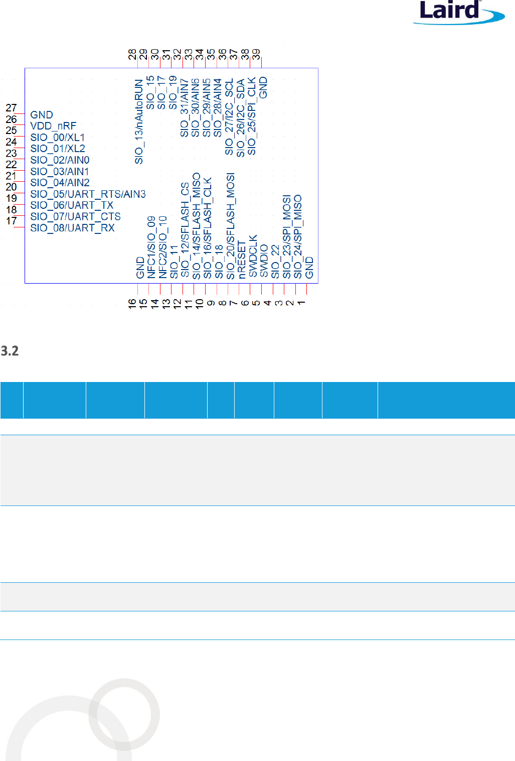
Figure 3: BL652-Sx module pin-out (top view)
Pin Definitions
Table 2: Pin definitions
Pin
#
Pin Name
Default
Function
Alternate
Function
In/
Out
Pull
Up/
Down
nRF52832
QFN Pin
nRF52832
QFN Name
Comment
1
GND
-
-
-
-
-
-
-
2
SIO_24/
SPI_MISO
SIO_24
SPI_MISO
IN
PULL-
UP
29
PO.24
Laird Devkit: SPI EEPROM.
SPI_Eeprom_MISO, Input.
SPIOPEN() in smartBASIC selects
SPI function; MOSI and CLK are
outputs when in SPI master mode.
3
SIO_23/
SPI_MOSI
SIO_23
SPI_MOSI
IN
PULL-
UP
28
PO.23
Laird Devkit: SPI EEPROM.
SPI_Eeprom_MOSI, Output
SPIOPEN() in smartBASIC selects
SPI function, MOSI and CLK are
outputs in SPI master.
4
SIO_22
SIO_22
IN
PULL-
UP
27
PO.22
Laird Devkit: SPI EEPROM.
SPI_Eeprom_CS, Input
5
SWDIO
SWDIO
-
-
PULL-
UP
26
SWDIO
-
BL652
Datasheet
Embedded Wireless Solutions Support Center:
http://ews-support.lairdtech.com
www.lairdtech.com/bluetooth
11
© Copyright 2016 Laird. All Rights Reserved
Americas: +1-800-492-2320
Europe: +44-1628-858-940
Hong Kong: +852 2923 0610
Pin
#
Pin Name
Default
Function
Alternate
Function
In/
Out
Pull
Up/
Down
nRF52832
QFN Pin
nRF52832
QFN Name
Comment
6
SWDCLK
SWDCLK
-
-
PULL-
DOWN
25
SWDCLK
-
7
nRESET
nRESET
-
IN
PULL-
UP
24
PO.21/
nRESET
System Reset (Active Low)
8
SIO_20/
SFLASH_MOSI
SIO_20
SFLASH_MOSI
IN
PULL-
UP
23
PO.20
Laird Devkit: Optional External
serial SPI flash for data logging
purpose.
High level API in smartBASIC can
be used for fast access using
open/close/read/write API
functions.
9
SIO_18
SIO_18
-
IN
PULL-
UP
21
PO.18
-
10
SIO_16/
SFLASH_CLK
SIO_16
SFLASH_CLK
IN
PULL-
UP
19
PO.16
Laird Devkit: Optional External
serial SPI flash for data logging
purpose.
High level API in smartBASIC can
be used for fast access using
open/close/read/write API
functions.
11
SIO_14/
SFLASH_MISO
SIO_14
SFLASH_MISO
IN
PULL-
UP
17
PO.14
12
SIO_12/
SFLASH_CS
SIO_12
SFLASH_CS
IN
PULL-
UP
15
PO.12
13
SIO_11
SIO_11
-
IN
PULL-
UP
14
PO.11
Laird Devkit: BUTTON1
14
NFC2/
SIO_10
NFC2
SIO_10
IN
-
12
PO.10/NFC2
-
15
NFC1/
SIO_09
NFC1
SIO_09
IN
-
11
PO.09/NFC1
-
16
GND
-
-
-
-
-
-
-
17
SIO_08/
UART_RX
SIO_08
UART_RX
IN
PULL-
UP
10
PO.08
UARTCLOSE() selects DIO
functionality
UARTOPEN() selects UART
COMMS behaviour
18
SIO_07/
UART_CTS
SIO_07
UART_CTS
IN
PULL-
DOWN
9
PO.07
19
SIO_06/
UART_TX
SIO_06
UART_TX
OUT
Set
High in
FW
8
PO.06
20
SIO_05/
UART_RTS/
AIN3
SIO_05
UART_RTS/
AIN3
OUT
Set Low
in FW
7
PO.05/AIN3
21
SIO_04/
AIN2
SIO_04
AIN2
IN
PULL-
UP
6
PO.04/AIN2
Internal pull-down
22
SIO_03/
AIN1
SIO_03
AIN1
IN
PULL-
UP
5
PO.03/AIN1
Laird Devkit: Temp Sens Analog
or Arduino Analog
BL652
Datasheet
Embedded Wireless Solutions Support Center:
http://ews-support.lairdtech.com
www.lairdtech.com/bluetooth
12
© Copyright 2016 Laird. All Rights Reserved
Americas: +1-800-492-2320
Europe: +44-1628-858-940
Hong Kong: +852 2923 0610
Pin
#
Pin Name
Default
Function
Alternate
Function
In/
Out
Pull
Up/
Down
nRF52832
QFN Pin
nRF52832
QFN Name
Comment
23
SIO_02/
AIN0
SIO_02
AIN0
IN
PULL-
DOWN
4
PO.02/AIN0
Internal pull-down
24
SIO_01/
XL2
SIO_01
XL2
IN
PULL-
UP
3
PO.01/XL2
Laird Devkit: Optional 32.768kHz
crystal pad XL2
25
SIO_00/
XL1
SIO_00
XL1
IN
PULL-
UP
2
PO.00/XL1
Laird Devkit: Optional 32.768kHz
crystal pad XL1
26
VDD_nRF
-
-
-
-
-
-
1.7V to 3.6V
27
GND
-
-
-
-
-
-
-
-
SIO_13/
nAutoRUN
nAutoRUN
SIO_13
IN
PULL-
DOWN
16
PO.13
Laird Devkit: FTDI USB_DTR via
jumper on J12pin1-2.
29
SIO_15
SIO_15
-
IN
PULL-
UP
18
PO.15
Laird Devkit: BUTTON2
30
SIO_17
SIO_17
-
IN
PULL-
UP
20
PO.17
Laird Devkit: LED1
31
SIO_19
SIO_19
-
IN
PULL-
UP
22
PO.19
Laird Devkit: LED2
32
SIO_31/
AIN7
SIO_31
AIN7
IN
PULL-
UP
43
PO.31/AIN7
-
33
SIO_30/
AIN6
SIO_30
AIN6
IN
PULL-
UP
42
PO.30/AIN6
-
34
SIO_29/
AIN5
SIO_29
AIN5
IN
PULL-
UP
41
PO.29/AIN5
-
35
SIO_28/
AIN4
SIO_28
AIN4
IN
PULL-
UP
40
PO.28/AIN4
-
36
SIO_27/
I2C_SCL
SIO_27
I2C_SCL
IN
PULL-
UP
39
PO.27
Laird Devkit: I2C RTC chip. I2C
clock line.
37
SIO_26/
I2C_SDA
SIO_26
I2C_SDA
IN
PULL-
UP
38
PO.26
Laird Devkit: I2C RTC chip. I2C
data line.
38
SIO_25/
SPI_CLK
SIO_25
SPI_CLK
IN
PULL-
UP
37
PO.25
Laird Devkit: SPI EEPROM.
SPI_Eeprom_CLK, Output
SPIOPEN() in smartBASIC selects
SPI function, MOSI and CLK are
outputs when in SPI master mode.
39
GND
-
-
-
-
-
-
-
Pin Definition Notes:
Note 1
Secondary function is selectable in smartBASIC application.

BL652
Datasheet
Embedded Wireless Solutions Support Center:
http://ews-support.lairdtech.com
www.lairdtech.com/bluetooth
13
© Copyright 2016 Laird. All Rights Reserved
Americas: +1-800-492-2320
Europe: +44-1628-858-940
Hong Kong: +852 2923 0610
Pin Definition Notes:
Note 2
DIO = Digital Input or Output.
I/O voltage level tracks VCC.
Note 3
AIN = Analog Input
Note 4
DIO or AIN functionality is selected using the GpioSetFunc() function in smartBASIC.
Note 5
AIN configuration selected using GpioSetFunc() function.
Note 6
I2C, UART, SPI controlled by xxxOPEN() functions in smartBASIC.
Note 7
SIO_5 to SIO_8 are DIO by default when $autorun$ app runs on power-up.
Note 8
JTAG (two-wire SWD interface), pin 5 (SWDIO) and pin 6 (SWDCLK).
JTAG is NOT required for customer use. Upgrading smartBASIC runtime engine firmware or loading
the smartBASIC applications is done using the UART interface.
Note 9
Pull the nRESET pin (pin 7) low for minimum 100 milliseconds to reset the BL652.
Note 10
SPI CS is created by using any spare SIO pin within their smartBASIC application script allowing multi-
dropping.
Note 11
The SIO_02 pin must be pulled high externally to enable an OTA (over-the-air) smartBASIC
application download. Refer to the latest firmware release documentation for details.
Note 12
Ensure that SIO_02 (pin 23) and AutoRUN (pin 28) are not both high (externally), in that state, the
UART is bridged to Virtual Serial Port service; the BL652 module does not respond to AT commands
and cannot load smartBASIC application scripts.
Note 13
The smartBASIC runtime engine has DIO (Default Function) INPUT pins, which are set PULL-UP by
default. This avoids floating inputs (which can cause current consumption to drive with time in low
power modes (such as StandbyDoze). You can disable the PULL-UP through your smartBASIC
application.
All of the SIO pins (with a default function of DIO) are inputs (apart from SIO_05 and SIO_08, which
are outputs):
SIO_06 (alternative function UART_TX) is an output, set High (in the firmware).
SIO_05 (alternative function UART_RTS) is an output, set Low (in the firmware).
SIO_08 (alternative function UART_RX) is an input, set with internal pull-up (in the firmware).
SIO_07 (alternative function UART_CTS) is an input, set with internal pull-down (in the
firmware).

BL652
Datasheet
Embedded Wireless Solutions Support Center:
http://ews-support.lairdtech.com
www.lairdtech.com/bluetooth
14
© Copyright 2016 Laird. All Rights Reserved
Americas: +1-800-492-2320
Europe: +44-1628-858-940
Hong Kong: +852 2923 0610
Pin Definition Notes:
SIO_02 is an input set with internal pull-down (in the firmware). It is used for OTA downloading
of smartBASIC applications. Refer to the latest firmware release documentation for details.
Note 14
Not required for BL652 module normal operation. If you fit an external serial (SPI) flash for data
logging purposes, then that external serial (SPI) flash must connect to BL652 module pins SIO_12
(SFLASH_CS), SIO_14 (SFLASH_MISO), SIO_16 (SFLASH_CLK), and SIO_20 (SFLASH_MOSI); in that
case, a high level API in smartBASIC can be used for fast access using open/close/read/write API
functions.
By default, these are GPIO pins. Only when in their FlashOpen() smartBASIC app are these lines
dedicated to SPI and for talking to the off-board flash.
If you decide to use an external serial (SPI) flash with BL652-SX-xx, then ONLY the manufacturer part
numbers below MUST be used:
4 Mbit Macronix MX25R4035F
http://www.macronix.com/Lists/DataSheet/Attachments/3288/MX25R4035F,%20Wide%20Ran
ge,%204Mb,%20v1.2.pdf
8 Mbit Macronix MX25R8035F
http://www.macronix.com/Lists/DataSheet/Attachments/3532/MX25R8035F,%20Wide%20Ran
ge,%208Mb,%20v1.2.pdf
smartBASIC does not provide access to any external serial (SPI) flash other than these part numbers.
Note 15
Not required for BL652 module normal operation. The on-chip 32.768kHz RC oscillator provides the
standard accuracy of ±250 ppm, with calibration required every 8seconds (default) to stay within
±250 ppm.
BL652 also allows as an option to connect an external higher accuracy (±20 ppm) 32.768 kHz crystal
to the BL652-SX-xx pins SIO_01/XL2 (pin 24) and SIO_00/XL1 (pin 25). This provides higher accuracy
protocol timing and helps with radio power consumption in the system standby doze/deep sleep
modes by reducing the time that the Rx window must be open.
The BL652 module is delivered with the integrated smartBASIC runtime engine firmware loaded (but no onboard
smartBASIC application script). Therefore it boots into AT command mode by default.
At reset, all SIO lines are configured as the defaults shown above.
SIO lines can be configured through the smartBASIC application script to be either inputs or outputs with pull-ups
or pull-downs. When an alternative SIO function is selected (such as I2C or SPI), the firmware does not allow the
setup of internal pull-up/pull-down. Therefore, when I2C interface is selected, pull-up resistors on I2C SDA and
I2C SCL must be connected externally as per I2C standard.
UART_RX, UART_TX, and UART_CTS are 3.3 V level logic (if VCC is 3.3 V; such as SIO pin I/O levels track VCC). For
example, when Rx and Tx are idle, they sit at 3.3 V (if VCC is 3.3 V). Conversely, handshaking pins CTS and RTS at
0V are treated as assertions.
BL652
Datasheet
Embedded Wireless Solutions Support Center:
http://ews-support.lairdtech.com
www.lairdtech.com/bluetooth
15
© Copyright 2016 Laird. All Rights Reserved
Americas: +1-800-492-2320
Europe: +44-1628-858-940
Hong Kong: +852 2923 0610
Pin 28 (nAutoRUN) is an input, with active low logic. In the development kit (DVK-BL652-xx) it is connected so
that the state is driven by the host’s DTR output line. The nAutoRUN pin must be externally held high or low to
select between the following two BL652 operating modes:
Self-contained Run mode (nAutoRUN pin held at 0V –this is the default (internal pull-down enabled))
Interactive/Development mode (nAutoRUN pin held at VCC)
The smartBASIC runtime engine firmware checks for the status of nAutoRUN during power-up or reset. If it is low
and if there is a smartBASIC application script named $autorun$, then the smartBASIC runtime engine firmware
executes the application script automatically; hence the name Self-contained Run Mode.
Electrical Specifications
3.3.1 Absolute Maximum Ratings
Absolute maximum ratings for supply voltage and voltages on digital and analogue pins of the module are listed
below; exceeding these values causes permanent damage.
Table 3: Maximum current ratings
Parameter
Min
Max
Unit
Voltage at VDD_nRF pin
-0.3
+3.9 (Note 1)
V
Voltage at GND pin
0
V
Voltage at SIO pin (at VDD_nRF≤3.6V)
-0.3
VDD_nRF +0.3
V
Voltage at SIO pin (at VDD_nRF≥3.6V)
-0.3
3.9
V
NFC antenna pin current (NFC1/2)
-
80
mA
Radio RF input level
-
10
dBm
Environmental
Storage temperature
-40
+85
ºC
MSL (Moisture Sensitivity Level)
-
3
-
ESD (as per EN301-489)
Conductive
Air Coupling
4
8
KV
KV
Flash Memory (Endurance) (Note 2)
-
10000
Write/erase cycles
Flash Memory (Retention)
-
10 years at 40°C
-
Maximum Ratings Notes:
Note 1
The absolute maximum rating for VCC pin (max) is 3.9V for the BL652-Sx-xx.
Note 2
Wear levelling is used in file system.
3.3.2 Recommended Operating Parameters
Table 4: Power supply operating parameters
Parameter
Min
Typ
Max
Unit
VDD_nRF (independent of DCDC)1
1.8
3.3
3.6
V
BL652
Datasheet
Embedded Wireless Solutions Support Center:
http://ews-support.lairdtech.com
www.lairdtech.com/bluetooth
16
© Copyright 2016 Laird. All Rights Reserved
Americas: +1-800-492-2320
Europe: +44-1628-858-940
Hong Kong: +852 2923 0610
Parameter
Min
Typ
Max
Unit
VCC Maximum ripple or noise2
-
-
10
mV
VCC rise time (0 to 1.7V)3
-
-
60
mS
Operating Temperature Range
-40
-
+85
ºC
Recommended Operating Parameters Notes:
Note 1
4.7 uF internal to module on VCC. In smartBASIC runtime engine firmware, use of the internal DCDC
convertor or LDO is decided by the underlying BLE stack.
Note 2
This is the maximum VCC ripple or noise (at any frequency) that does not disturb the radio.
Note 3
The on-board power-on reset circuitry may not function properly for rise times outside the noted
interval.
Table 5: Signal levels for interface, SIO
Parameter
Min
Typ
Max
Unit
VIH Input high voltage
0.7 VDD_nRF
VDD_nRF
V
VIL Input low voltage
VSS
0.3 x VDD_nRF
V
VOH Output high voltage
(std. drive, 0.5mA) (Note 1)
(high-drive, 3mA) (Note 1)
(high-drive, 5mA) (Note 2)
VDD_nRF -0.4
VDD_nRF -0.4
VDD_nRF -0.4
VDD_nRF
VDD_nRF
VDD_nRF
V
V
VOL Output low voltage
(std. drive, 0.5mA) (Note 1)
(high-drive, 3mA) (Note 1)
(high-drive, 5mA) (Note 2)
VSS
VSS
VSS
VSS+0.4
VSS+0.4
VSS+0.4
V
V
VOL Current at VSS+0.4V,Output set low
(std. drive, 0.5mA) (Note 1)
(high-drive, 3mA) (Note 1)
(high-drive, 5mA) (Note 2)
1
3
6
2
-
10
4
-
15
mA
mA
mA
VOL Current at VDD_nRF -0.4, Output set low
(std. drive, 0.5mA) (Note 1)
(high-drive, 3mA) (Note 1)
(high-drive, 5mA) (Note 2)
1
3
6
2
-
9
4
-
14
mA
mA
mA
Pull up resistance
11
13
16
kΩ
Pull down resistance
11
13
16
kΩ
Pad capacitance
3
pF
Pad capacitance at NFC pads
4
pF
BL652
Datasheet
Embedded Wireless Solutions Support Center:
http://ews-support.lairdtech.com
www.lairdtech.com/bluetooth
17
© Copyright 2016 Laird. All Rights Reserved
Americas: +1-800-492-2320
Europe: +44-1628-858-940
Hong Kong: +852 2923 0610
Signal Levels Notes:
Note 1
For VDD_nRF≥1.7V. The smartBASIC firmware supports high drive (3 mA, as well as standard drive).
Note 2
For VDD_nRF≥2.7V. The smartBASIC firmware supports high drive (5 mA (since VDD_nRF≥2.7V), as
well as standard drive).
Table 6: SIO pin alternative function AIN (ADC) specification
Parameter
Min
Typ
Max
Unit
ADC Internal reference voltage
-1.5%
0.6 V
+1.5%
%
ADC pin input
internal selectable scaling
4, 2, 1, 1/2,
1/3, 1/4, 1/5
1/6
scaling
ADC input pin (AIN) voltage maximum without
damaging ADC w.r.t1
VCC Prescaling
0V-VDD_nRF 4, 2, 1, ½, 1/3, ¼, 1/5, 1/6
VDD+0.3
V
Configurable via smartBASIC
Resolution
8bit
mode
10bit mode
12bit mode
bits
Configurable via smartBASIC2
Acquisition Time, source resistance ≤10kΩ
Acquisition Time, source resistance ≤40kΩ
Acquisition Time, source resistance ≤100kΩ
Acquisition Time, source resistance ≤200kΩ
Acquisition Time, source resistance ≤400kΩ
Acquisition Time, source resistance ≤800kΩ
3
5
10
15
20
40
uS
uS
uS
uS
uS
uS
Conversion Time3
<2
uS
ADC input impedance (during operation)3
Input Resistance
Sample and hold capacitance at maximum gain
>1
2.5
MOhm
pF
Recommended Operating Parameters Notes:
Note 1
Stay within internal 0.6 V reference voltage with given pre-scaling on AIN pin and do not violate ADC
maximum input voltage (for damage) for a given VCC, e.g. If VCC is 3.6V, you can only expose AIN pin
to VDD+0.3 V. Default pre-scaling is 1/6 which configurable via smartBASIC.
Note 2
smartBASIC runtime engine firmware allows configurable resolution (8-bit, 10-bit or 12-bit mode)
and acquisition time. The sampling frequency is limited by the sum of sampling time and acquisition
time. The maximum sampling time is 2us. For acquisition time of 3us the total conversion time is
therefore 5us, which makes maximum sampling frequency of 1/5us = 200kHz. Similarly, if acquisition
time of 40us chosen, then the conversion time is 42us and the maximum sampling frequency is
1/42us = 23.8kHz
Note 3
ADC input impedance is estimated mean impedance of the ADC (AIN) pins.
BL652
Datasheet
Embedded Wireless Solutions Support Center:
http://ews-support.lairdtech.com
www.lairdtech.com/bluetooth
18
© Copyright 2016 Laird. All Rights Reserved
Americas: +1-800-492-2320
Europe: +44-1628-858-940
Hong Kong: +852 2923 0610
3.3.3 nAutoRUN Pin and Operating Modes
Operating modes (refer to the smartBASIC guide for details):
Self-contained mode
Interactive/Development mode
Table 7: nAutoRUN pin
Signal Name
Pin #
I/O
Comments
nAutoRUN /(SIO_13)
28
I
Input with active low logic. Internal pull down (default).
Operating mode selected by nAutoRun pin status:
If Low (0V), runs $autorun$ if it exists
If High (VCC), runs via at+run (and file name of application)
Pin 28 (nAutoRUN) is an input, with active low logic. In the development board (DVK-BL652-xx) it is connected so
that the state is driven by the host’s DTR output line. nAutoRUN pin needs to be externally held high or low to
select between the two BL652 operating modes:
Self-contained Run mode (nAutoRUN pin held at 0V).
Interactive/Development mode (nAutoRUN pin held at VCC).
smartBASIC runtime engine firmware checks for the status of nAutoRUN during power-up or reset. If it is low
AND if there is a smartBASIC application named $autorun$, the smartBASIC runtime engine executes the
application automatically; hence the name self-contained run mode.
3.3.4 OTA (Over-the-Air) smartBASIC Application Download
Refer to latest firmware release documentation (firmware release notes and smartBASIC user guide) for details.
Table 8: OTA mode
Signal Name
Pin #
I/O
Comments
SIO_02
23
I
Internal pull down (default).
OTA mode selected by externally pulling-up SIO_02 pin:
High (VCC), then OTA smart BASIC application download is possible.
The OTA smartBASIC application download feature can be useful for production because it allows the module to
be soldered into an end product without pre-configuration; the application can then be downloaded over-the-air
once the product has been pre-tested.
Note: It is the smartBASIC application that is downloaded over-the-air and NOT the firmware. Since this is
principally designed for use in production with multiple programming stations in a locality, the
transmit power is limited (to lower Tx power). See the smartBASIC user guide for more details.
BL652
Datasheet
Embedded Wireless Solutions Support Center:
http://ews-support.lairdtech.com
www.lairdtech.com/bluetooth
19
© Copyright 2016 Laird. All Rights Reserved
Americas: +1-800-492-2320
Europe: +44-1628-858-940
Hong Kong: +852 2923 0610
4 POWER CONSUMPTION
Data taken at VCC_nRF of 3.0 V with internal (to chipset) LDO ON or with internal (to chipset) DCDC ON
(see Note 1) and 25ºC.
Power Consumption
Table 9: Power consumption
Parameter
Min
Typ
Max
Unit
Active mode ‘peak’ current (Note 1)
(Advertising or Connection)
Tx only run peak current @ Txpwr = +4 dBm
Tx only run peak current @ Txpwr = 0 dBm
Tx only run peak current @ Txpwr = -4 dBm
Tx only run peak current @ Txpwr = -8 dBm
Tx only run peak current @ Txpwr = -12 dBm
Tx only run peak current @ Txpwr = -16 dBm
Tx only run peak current @ Txpwr = -20 dBm
With DCDC [with LDO]
7.5 [16.6]
5.3 [11.6]
4.2 [9.3]
3.8 [8.4]
3.5 [7.7]
3.3 [7.3]
3.2 [7.0]
mA
mA
mA
mA
mA
mA
mA
Tx Whisper mode 1 (Note 2)
Tx only run peak current @ Txpwr = -40 dBm
2.7 [5.9]
mA
Active Mode
Rx only ‘peak’ current (Note 2)
5.4 [11.7]
mA
Ultra Low Power Mode 1 (Note 2)
Standby Doze, no RAM retention
1.2
uA
Ultra Low Power Mode 2 (Note 3)
Deep Sleep (no RAM retention)
400
nA
Active Mode Average current (Note 4)
Advertising Average Current draw
Max, with advertising interval (min) 20 mS
Min, with advertising interval (max) 10240 mS
Connection Average Current draw
Max, with connection interval (min) 7.5 mS
Min, with connection interval (max) 4000 mS
~511
~3.2
~513
~2.9
uA
uA
uA
uA
Power Consumption Notes:
Note 1
This is for Peak Radio Current only, but there is additional current due to the MCU, refer to Table 12
and Table 15 for the peak and "Average Advert/connection (burst) current" consumption profile
(with DCDC on) during advertising and connection versus TX power. In smartBASIC runtime engine
firmware, use of the internal DCDC convertor or LDO is decided by the underlying BLE stack.
Note 2
BL652-Sx-xx: Standby Doze is 1.2uA typical. Standby Doze is entered automatically (when a waitevent
statement is encountered within a smartBASIC application script). In Standby Doze, all peripherals

BL652
Datasheet
Embedded Wireless Solutions Support Center:
http://ews-support.lairdtech.com
www.lairdtech.com/bluetooth
20
© Copyright 2016 Laird. All Rights Reserved
Americas: +1-800-492-2320
Europe: +44-1628-858-940
Hong Kong: +852 2923 0610
that are enabled stay on and may re-awaken the chip. Depending on active peripherals, current
consumption ranges from ~1.2 µA to 270 uA (when UART is ON). See individual peripherals current
consumption data in the Peripheral Block Current Consumption section. smartBASIC runtime engine
firmware has added new functionality to detect GPIO change with no current consumption cost, it is
possible to close the UART and get to the 1.2uA current consumption regime and still be able to
detect for incoming data and be woken up so that the UART can be re-opened at expense of losing
that first character.
Note 3
In Deep Sleep, everything is disabled and the only wake-up sources (including NFC to wakeup) are
reset and changes on SIO or NFC pins on which sense is enabled. The current consumption seen is
~400 nA typical in BL652-Sx-xx.
smartBASIC runtime engine firmware requires a hardware reset to come out of deep sleep.
smartBASIC runtime engine firmware also allows coming out from Deep Sleep to Standby Doze
through GPIO signal through the reset vector. Deep Sleep mode is entered with a command in
smartBASIC application script.
Note 4
Data taken with a transmit power of 4 dBm and all peripherals off (UART OFF after radio event), slave
latency of 0 (in a connection). Average current consumption depends on a number of factors
(including Tx power, VCC, accuracy of 32MHz and 32.768 kHz). With these factors fixed, the largest
variable is the advertising or connection interval set.
Advertising Interval range:
20 milliseconds to 10240 milliseconds in multiples of 0.625 milliseconds for the following Advert
type: ADV_IND and ADV_DIRECT_IND
100 milliseconds to 10240 milliseconds in multiples of 0.625 milliseconds for the following
Advert types: ADV_SCAN_IND and ADV_NONCONN_IND
For advertising timeout, if the advert type is ADV_DIRECT_IND, then the timeout is limited to
1.28 seconds (1280 milliseconds).
For an advertising event:
The minimum average current consumption is when the advertising interval is large 10240 mS
(although this may cause long discover times (for the advertising event) by scanners
The maximum average current consumption is when the advertising interval is small 20 mS
Other factors that are also related to average current consumption include the advertising
payload bytes in each advertising packet and whether it’s continuously advertising or
periodically advertising.
Connection Interval range:
7.5 milliseconds to 4000 milliseconds in multiples of 1.25 milliseconds.
For a connection event:
The minimum average current consumption is when the connection interval is large 4000
milliseconds
The maximum average current consumption is with the shortest connection interval of 7.5 ms;
no slave latency.
BL652
Datasheet
Embedded Wireless Solutions Support Center:
http://ews-support.lairdtech.com
www.lairdtech.com/bluetooth
21
© Copyright 2016 Laird. All Rights Reserved
Americas: +1-800-492-2320
Europe: +44-1628-858-940
Hong Kong: +852 2923 0610
Other factors that are also related to average current consumption include:
Whether transmitting six packets per connection interval with each packet containing 20 bytes
(which is the maximum for each packet)
An inaccurate 32.768 kHz master clock accuracy would increase the average current
consumption.
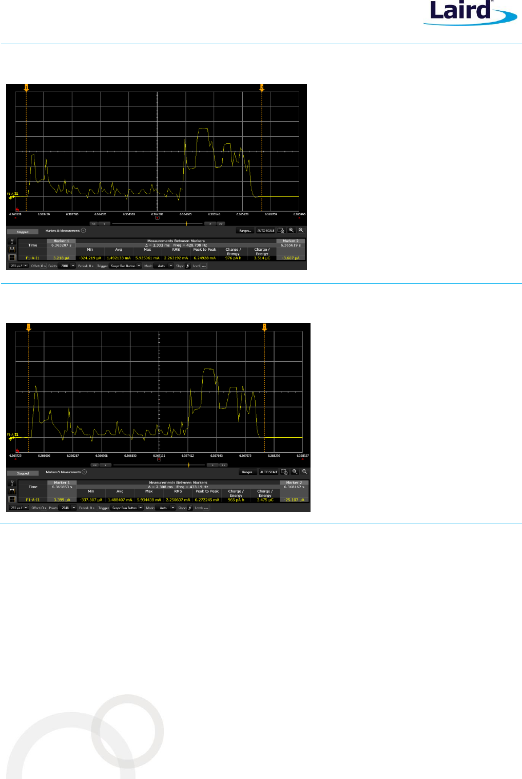
Measured Current Waveforms during Advertising and Connection
The following figures illustrate current waveforms observed as the BL652 module performs advertising and
connection functionality.
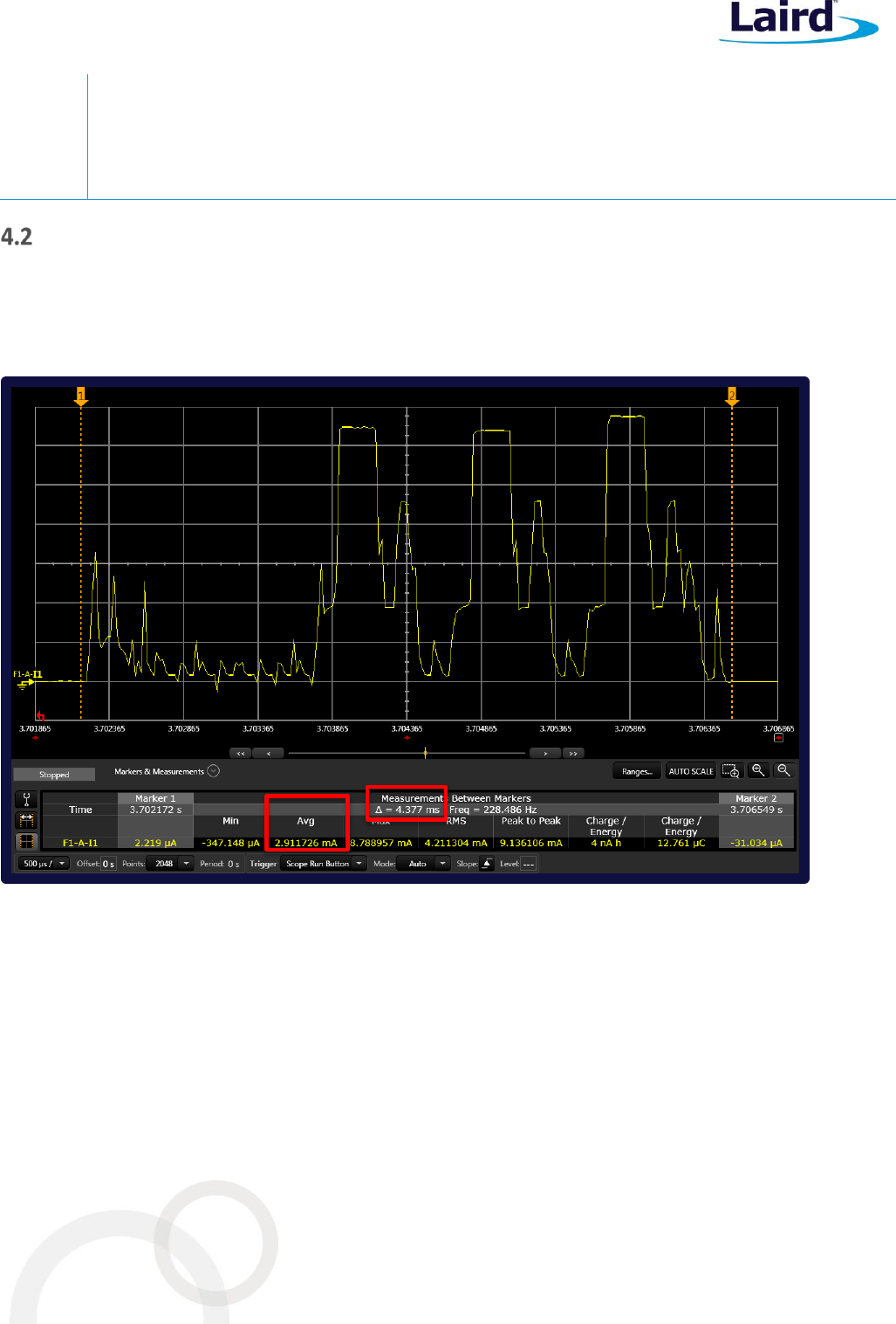
TX power – 4 dBm
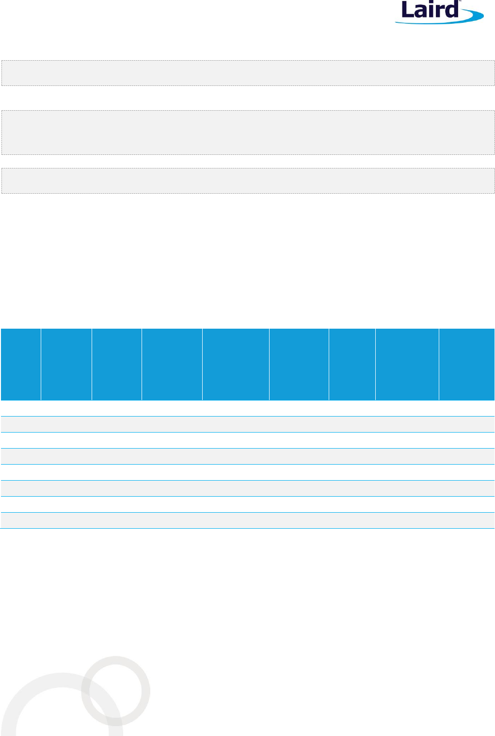
Advert duration ~4.377 ms
29 byte payload
Advertising interval – 20 ms
Figure 4: Typical peak current consumption profile (with DCDC ON) during advertising in slave mode @ TX PWR +4 dBm. UART is OFF
TX: <8.8 mA
TX: <8.8 mA
TX: 8.8 mA
RX: 6 mA
Average current for BLE Advert
RX: 6 mA
RX: 6 mA
BL652
Datasheet
Embedded Wireless Solutions Support Center:
http://ews-support.lairdtech.com
www.lairdtech.com/bluetooth
22
© Copyright 2016 Laird. All Rights Reserved
Americas: +1-800-492-2320
Europe: +44-1628-858-940
Hong Kong: +852 2923 0610
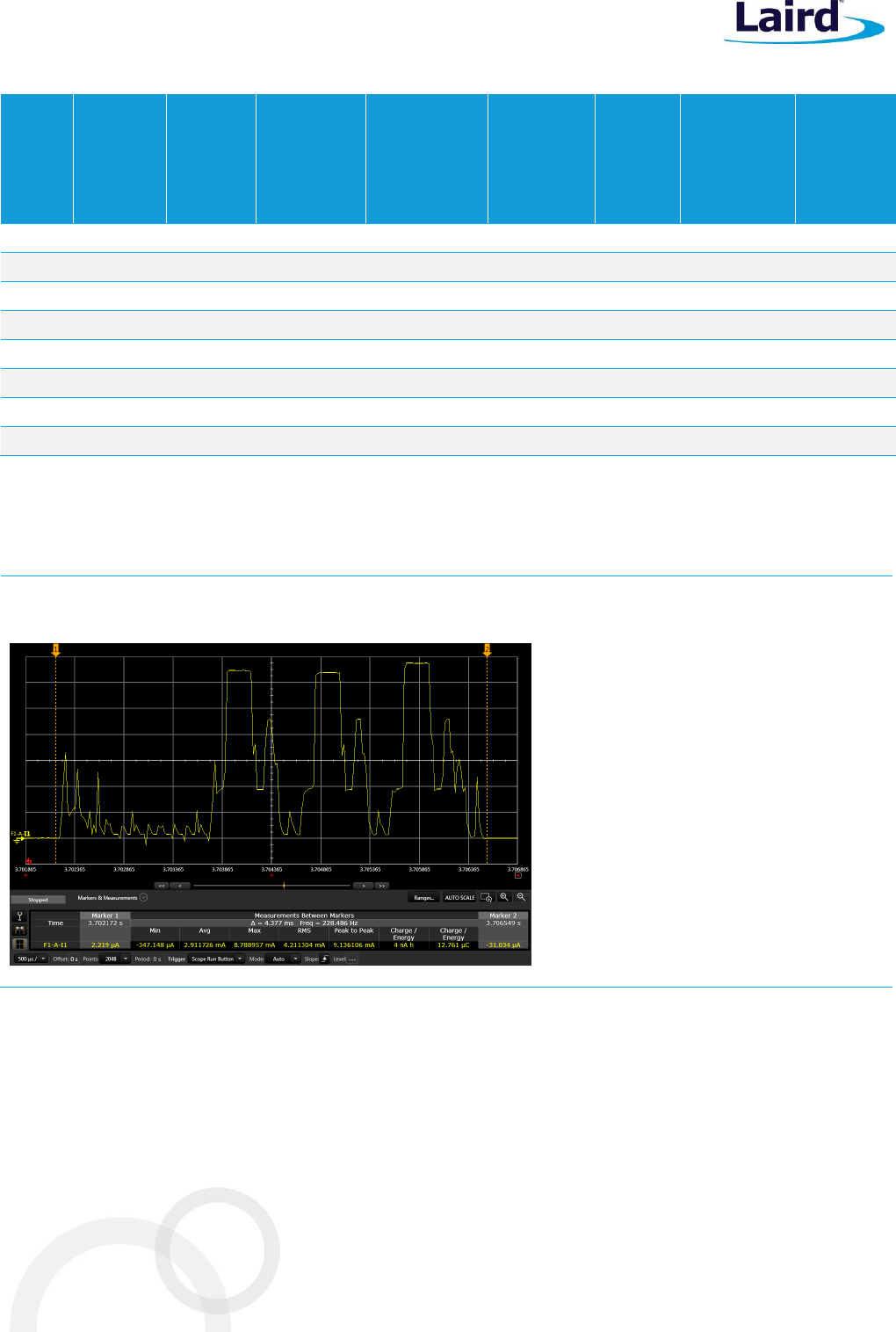
TX power – 4 dBm
Interval – 7.5 ms
29 byte payload
Advertising interval – 20 ms
Figure 5: Typical peak current consumption profile (with DCDC ON) during data connection event in slave mode @ TX PWR +4dBm
UART is OFF
Note: In the above pictures, UART is OFF. Y-axis current (1.3 mA per square).
To make things easier the average current during the whole BLE event is shown in the plot above, and then the
BLE event total charge consumption is found by multiplying the average current over the BLE event with the
length of the event. This charge can then be used to extrapolate the average current for different advertising
intervals, by dividing by the interval. Then the StandbyDoze (IDLE) current must be added to give the total
average current. In this example we can calculate the average current to be:
The total charge of the BLE event:
BLE_charge = BLE_avg * BLE_length
The average current consumed by the BLE event for a specific interval:
BLE_avg = BLE_charge / (BLE_interval + perturbation)
The perturbation is given as a random number between 0 and 10 milliseconds added to the interval to prevent
advertisers to periodically transmit at the exact same time. This averages to 5 milliseconds.
TX: 8.55 mA
RX: 6 mA
Average current for BLE connection
BL652
Datasheet
Embedded Wireless Solutions Support Center:
http://ews-support.lairdtech.com
www.lairdtech.com/bluetooth
23
© Copyright 2016 Laird. All Rights Reserved
Americas: +1-800-492-2320
Europe: +44-1628-858-940
Hong Kong: +852 2923 0610
Adding the IDLE current (StandbyDoze mode) to the inactive part of the interval:
TOT_avg = BLE_avg + IDLE * (BLE_interval - BLE_length) / BLE_interval
Performing the calculation with the numbers 25mS advertising internal and TX power for 4dBm for example:
BLE_charge = 4.377 ms * 2.91 mA = 12.74 uC
BLE_avg = 12.74 uC / 25 ms + 5 ms) = 509.78 uA
TOT_avg = 509.78 uA + 2 uA * (25 ms - 4.377 ms)/25 ms = 511.43 uA
Table 10 and Table 11 display the measured "Average Advert (Burst) current" (for a given TX power) which can be
used to calculate the Total average current for any advertising interval.
Table 12 and Table 13 display the measured "Average Connection (Burst) current" (for a given TX power) which
can be used to calculate the Total average current for any connection interval.
The following table (Table 10) shows the measured total average current consumption profile (with DCDC on)
during advertising in slave mode versus TX power for a minimum advertising interval of 25 milliseconds. Note
that UART is off.
Table 10: Measured total average current consumption profile – for a minimum advertising interval of 25 ms
TX
Power
(dBm)
Average
Advert
(Burst)
Current
(uA)
Average
Advert
(Burst)
Duration
(mS)
BLE
Advert
Charge
(uC)
BLE Advert
Interval
20 mS plus
5 mS
Perturbation
BLE
Advert
Average
(uA)
Max
Standby
Doze
Current
(uA)
BLE Advert
Interval
20 mS plus
5 mS
Pertubation
Total
Average
Current
(uA)
4
2911.726
4.377
12744.625
25
509.785
2
25
511.435
0
2431.095
4.377
10640.903
25
425.636
2
25
427.286
-4
2163.884
4.377
9471.320
25
378.853
2
25
380.503
-8
2151.602
4.377
9417.562
25
376.702
2
25
378.352
-12
2086.596
4.377
9133.031
25
365.321
2
25
366.971
-16
2052.041
4.377
8981.783
25
359.271
2
25
360.921
-20
2029.615
4.377
8883.625
25
355.345
2
25
356.995
-40
1960.112
4.377
8579.410
25
343.177
2
25
344.826
The following table (Table 11) shows the measured total average current consumption profile (with DCDC on)
during advertising in slave mode versus TX power for a maximum advertising interval of 10240 milliseconds. Note
that UART is off.
BL652
Datasheet
Embedded Wireless Solutions Support Center:
http://ews-support.lairdtech.com
www.lairdtech.com/bluetooth
24
© Copyright 2016 Laird. All Rights Reserved
Americas: +1-800-492-2320
Europe: +44-1628-858-940
Hong Kong: +852 2923 0610
Table 11: Measured total average current consumption profile – for a minimum advertising interval of 10240 ms
TX
Power
(dBm)
Average
Advert
(Burst)
Current
(uA)
Average
Advert
(Burst)
Duration
(mS)
BLE
Advert
Charge
(uC)
BLE Advert
Interval
10240 mS
plus 5 mS
Perturbation
BLE
Advert
Average
(uA)
Max
Standby
Doze
Current
(uA)
BLE Advert
Interval
10240 mS
plus 5 mS
Perturbation
Total
Average
Current
(uA)
4
2911.726
4.377
12744.625
10245
1.244
2
10245
3.243
0
2431.095
4.377
10640.903
10245
1.039
2
10245
3.038
-4
2163.884
4.377
9471.320
10245
0.924
2
10245
2.924
-8
2151.602
4.377
9417.562
10245
0.919
2
10245
2.918
-12
2086.596
4.377
9133.031
10245
0.891
2
10245
2.891
-16
2052.041
4.377
8981.783
10245
0.877
2
10245
2.876
-20
2029.615
4.377
8883.625
10245
0.867
2
10245
2.866
-40
1960.112
4.377
8579.410
10245
0.837
2
10245
2.837
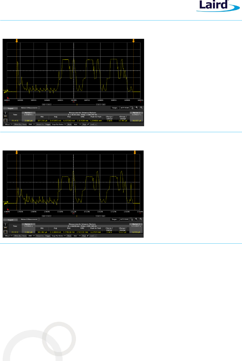
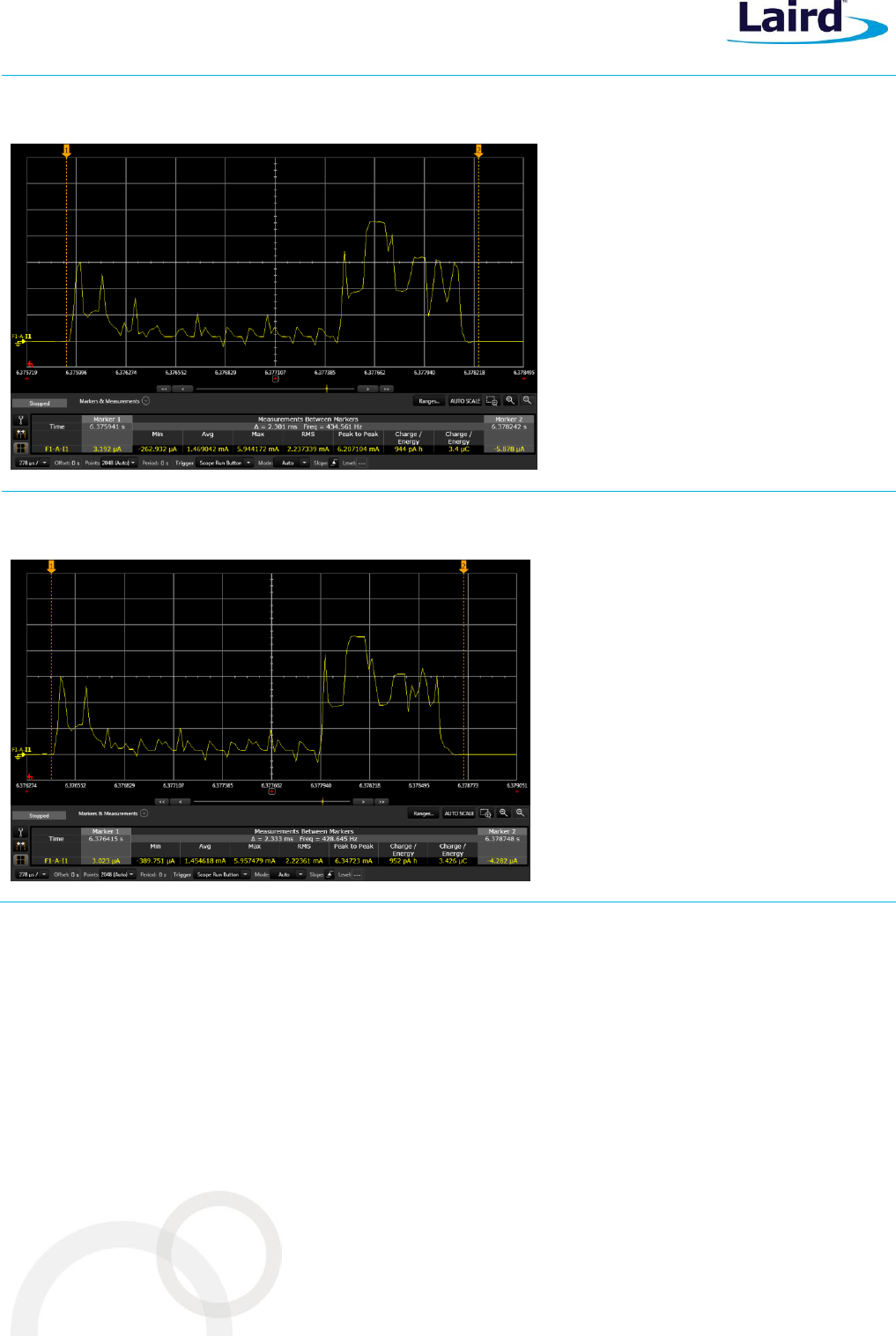
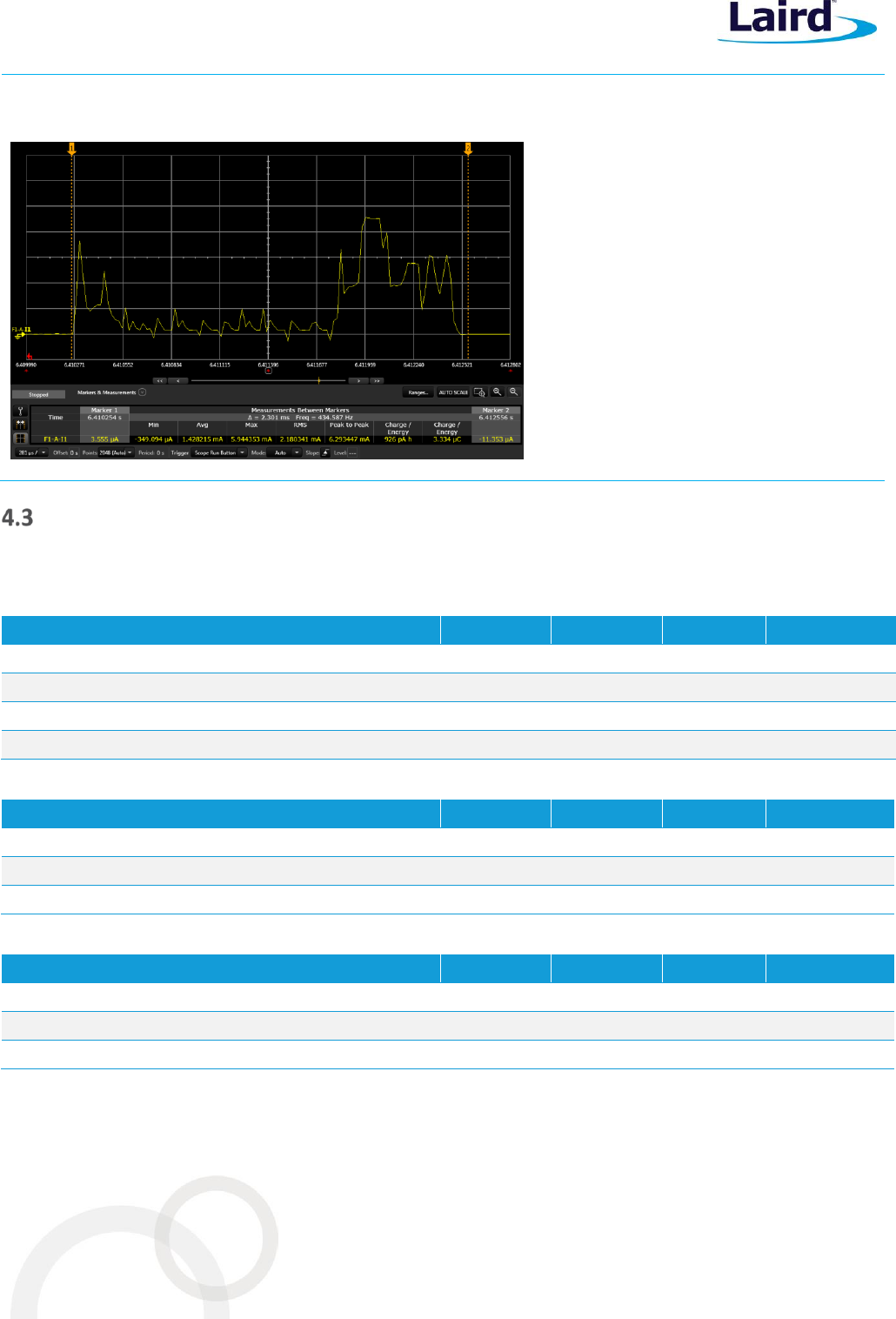
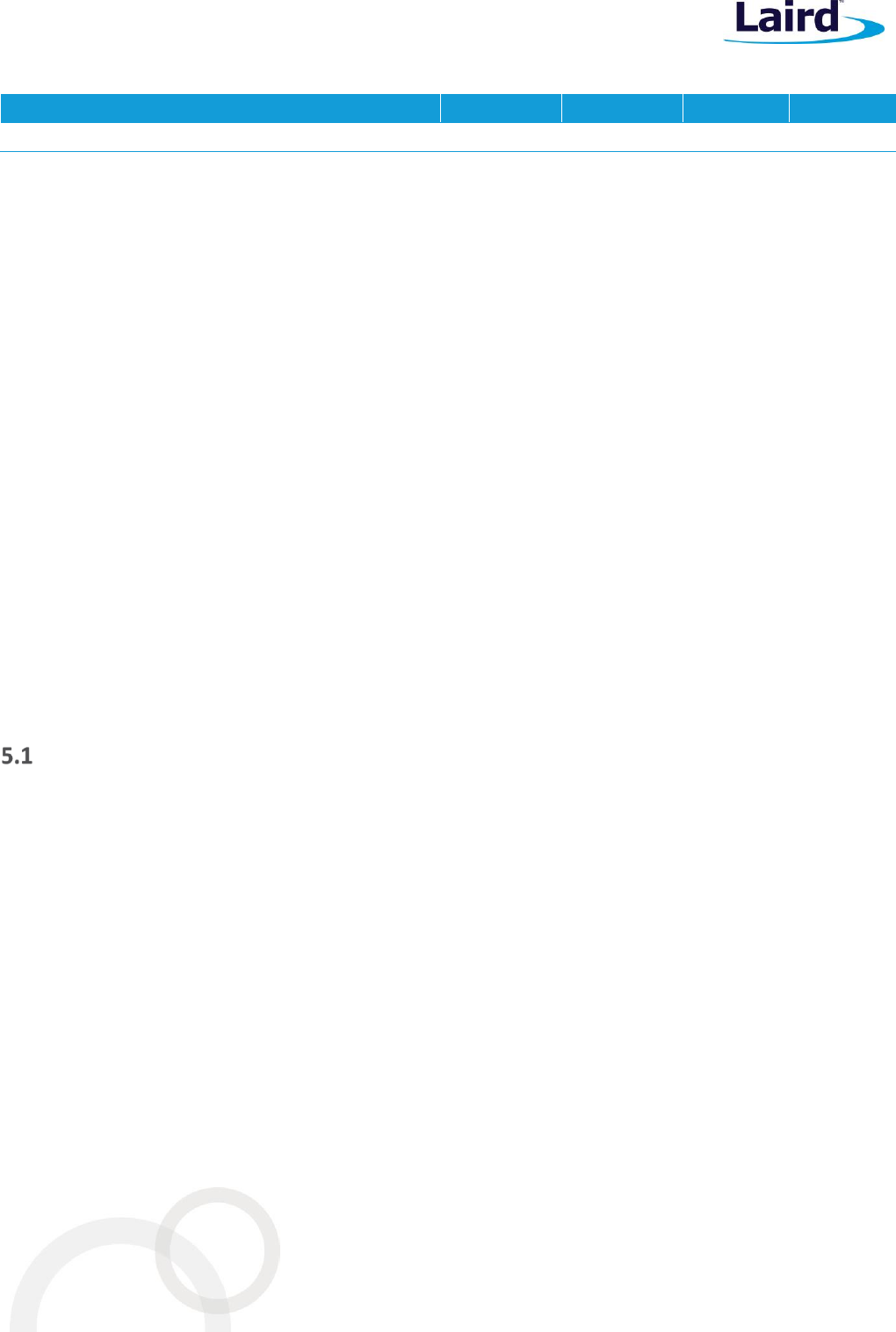
Table 12 displays measured peak and "Average Advert (burst) current" consumption profile (with DCDC on)
during advertising in slave mode versus TX power. Between Marker 1 and 2 is the average BLE advert current.
Table 12: Measured average advert (burst) current consumption profiles (with DCDC on) during advertising in slave mode vs TX power
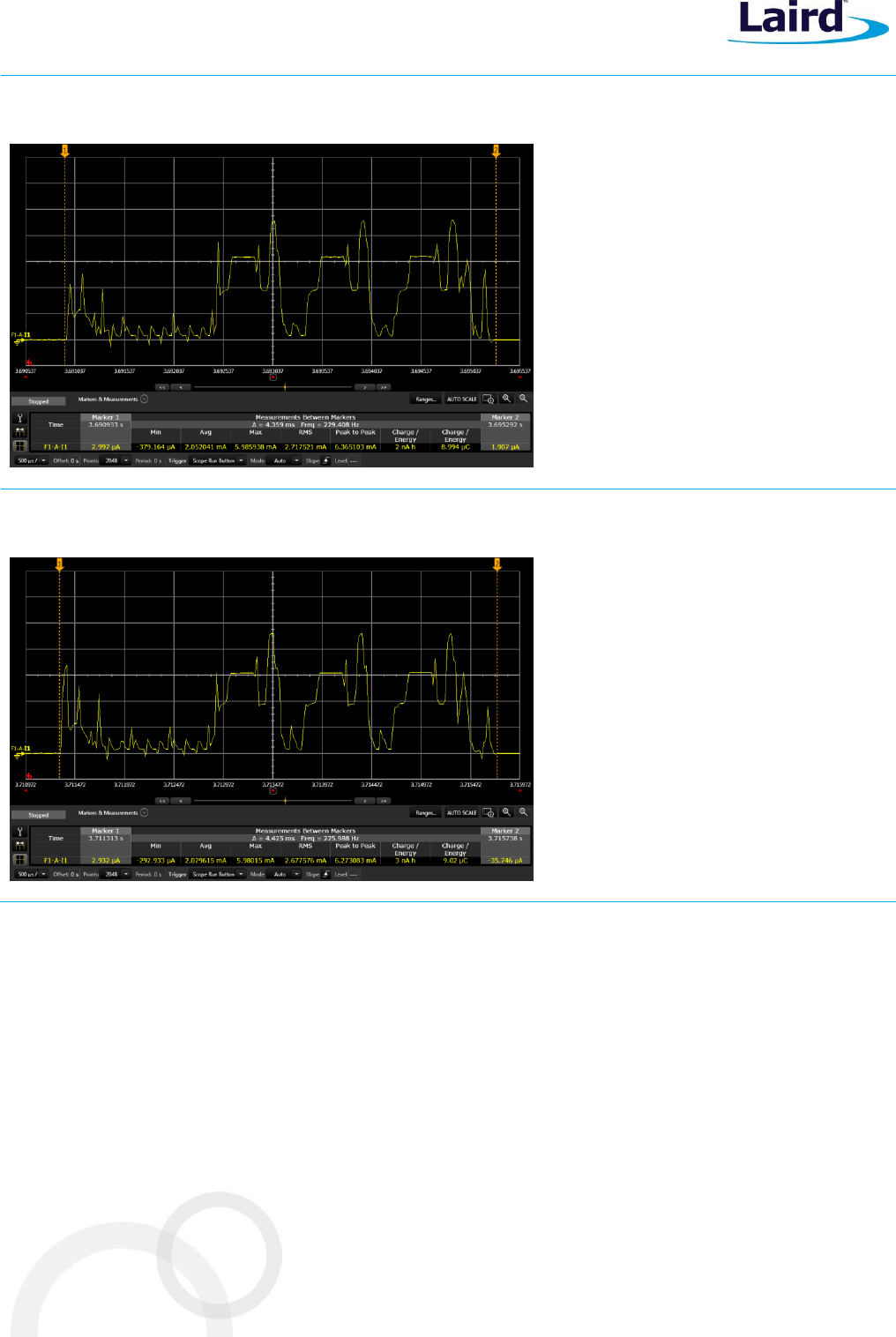
TX power: 4 dBm
Advert
29 byte payload
20 ms interval
Average BLE advert current burst
(excluding advertising interval): 2.911 mA
Aside:
Peak TX current: 8.8 mA
Peak RX current: 6 mA
BL652
Datasheet
Embedded Wireless Solutions Support Center:
http://ews-support.lairdtech.com
www.lairdtech.com/bluetooth
25
© Copyright 2016 Laird. All Rights Reserved
Americas: +1-800-492-2320
Europe: +44-1628-858-940
Hong Kong: +852 2923 0610
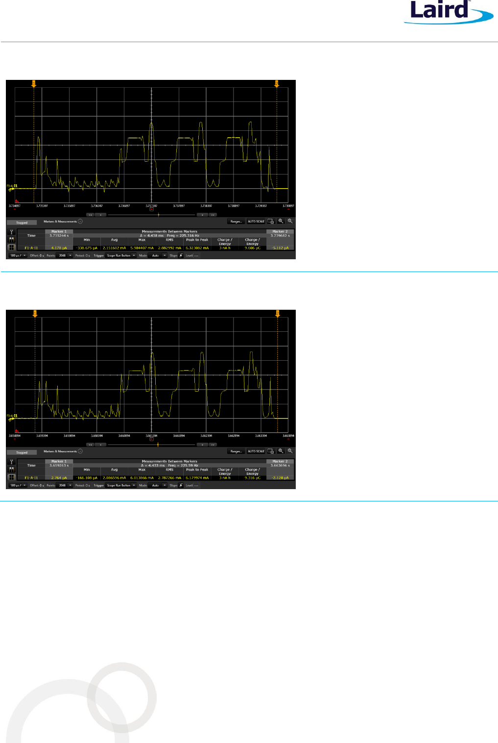
TX power: 0 dBm
Advert
29 byte payload
20 ms interval
Average BLE advert current burst
(excluding advertising interval): 2.431 mA
Aside:
Peak TX current: 6 mA
Peak RX current: 6 mA
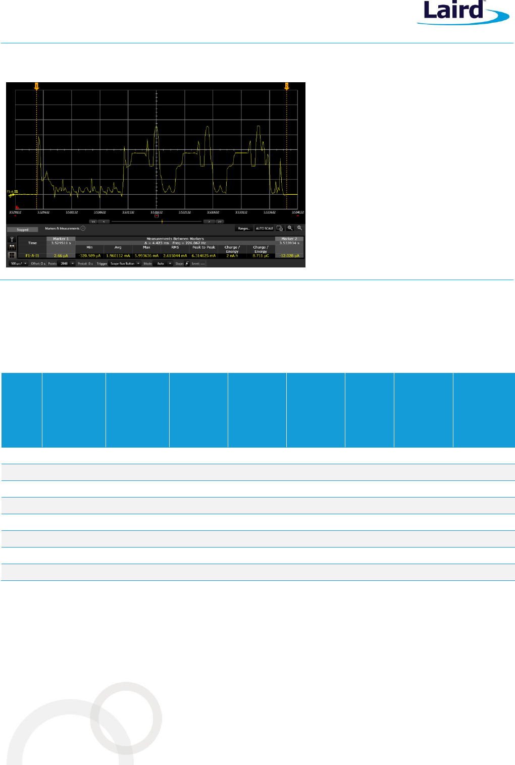
TX power: -4 dBm
Advert
29 byte payload
20 ms interval
Average BLE advert current burst
(excluding advertising Interval): 2.163 mA
Aside:
Peak TX current: 4.98 mA
Peak RX current: 5.99 mA
BL652
Datasheet
Embedded Wireless Solutions Support Center:
http://ews-support.lairdtech.com
www.lairdtech.com/bluetooth
26
© Copyright 2016 Laird. All Rights Reserved
Americas: +1-800-492-2320
Europe: +44-1628-858-940
Hong Kong: +852 2923 0610
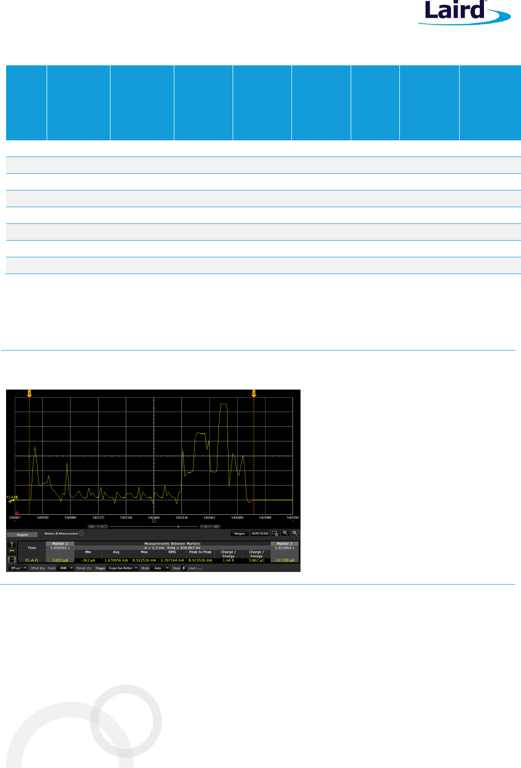
TX power: -8 dBm
Advert
29 byte payload
20 ms interval
Average BLE advert current burst
(excluding advertising Interval): 2.151 mA
Aside:
Peak TX current: 4.59 mA
Peak RX current: 5.98 mA
TX power: -12 dBm
Advert
29 byte payload
20 ms interval
Average BLE advert current burst
(excluding advertising Interval): 2.086 mA
Aside:
Peak TX current: 4.34 mA
Peak RX current: 5.99 mA
BL652
Datasheet
Embedded Wireless Solutions Support Center:
http://ews-support.lairdtech.com
www.lairdtech.com/bluetooth
27
© Copyright 2016 Laird. All Rights Reserved
Americas: +1-800-492-2320
Europe: +44-1628-858-940
Hong Kong: +852 2923 0610
TX power: -16 dBm
Advert
29 byte payload
20 ms interval
Average BLE advert current burst
(excluding advertising Interval): 2.052 mA
Aside:
Peak TX current: 4.16 mA
Peak RX current: 5.99 mA
TX power: -20 dBm
Advert
29 byte payload
20 ms interval
Average BLE advert current burst
(excluding advertising Interval): 2.029 mA
Aside:
Peak TX current: 4.03 mA
Peak RX current: 5.99 mA
BL652
Datasheet
Embedded Wireless Solutions Support Center:
http://ews-support.lairdtech.com
www.lairdtech.com/bluetooth
28
© Copyright 2016 Laird. All Rights Reserved
Americas: +1-800-492-2320
Europe: +44-1628-858-940
Hong Kong: +852 2923 0610
TX power: -40 dBm
Advert
29 byte payload
20 ms interval
Average BLE advert current burst
(excluding advertising Interval): 1.960 mA
Refer to table for worked out total BLE
advert average current for given
advertising interval.
Aside:
Peak TX current: 3.6 mA
Peak RX current: 6.01 mA
Table 13 and Table 14 has the measured "Average Connection (Burst) current" (for a given TX power) which can
be used to calculate the Total average current for any connection interval.
Table 13: Measured Total average current consumption profile (with DCDC ON) during connection in slave mode versus TX POWER for
minimum Connection interval of 7.5 mS. UART is OFF
TX
power
(dBm)
Average
Connection
(Burst)
Current (uA)
Average
Connection
(Burst)
Duration
(mS)
BLE
Connection
Charge
(uC)
BLE
Connection
Interval
(mS)
BLE
Connection
Average
(uA)
Max
Standby
Doze
Current
(uA)
BLE
Connection
Interval
7.5 ms
Total
Average
Current
(uA)
4
1670.956
2.3
3843.199
7.5
512.427
2
7.5
513.813
0
1560.069
2.3
3588.159
7.5
478.421
2
7.5
479.808
-4
1513.156
2.3
3480.259
7.5
464.035
2
7.5
465.421
-8
1492.133
2.3
3431.906
7.5
457.587
2
7.5
458.974
-12
1488.407
2.3
3423.336
7.5
456.445
2
7.5
457.831
-16
1469.042
2.3
3378.797
7.5
450.506
2
7.5
451.893
-20
1454.618
2.3
3345.621
7.5
446.083
2
7.5
447.470
-40
1428.215
2.3
3284.895
7.5
437.986
2
7.5
439.373
BL652
Datasheet
Embedded Wireless Solutions Support Center:
http://ews-support.lairdtech.com
www.lairdtech.com/bluetooth
29
© Copyright 2016 Laird. All Rights Reserved
Americas: +1-800-492-2320
Europe: +44-1628-858-940
Hong Kong: +852 2923 0610
Table 14: Measured Total average current consumption profile (with DCDC ON) during connection in slave mode versus TX POWER for
minimum Connection interval of 4000mS. UART is OFF
TX
power
(dBm)
Average
Connection
(Burst)
Current (uA)
Average
Connection
(Burst)
Duration
(mS)
BLE
Connection
Charge
(uC)
BLE
Connection
Interval
(mS)
BLE
Connection
Average
(uA)
Max
Standby
Doze
Current
(uA)
BLE
Connection
Interval
7.5 ms
Total
Average
Current
(uA)
4
1670.956
2.3
3843.199
4000
0.961
2
4000
2.960
0
1560.069
2.3
3588.159
4000
0.897
2
4000
2.896
-4
1513.156
2.3
3480.259
4000
0.870
2
4000
2.869
-8
1492.133
2.3
3431.906
4000
0.858
2
4000
2.857
-12
1488.407
2.3
3423.336
4000
0.856
2
4000
2.855
-16
1469.042
2.3
3378.797
4000
0.845
2
4000
2.844
-20
1454.618
2.3
3345.621
4000
0.836
2
4000
2.835
-40
1428.215
2.3
3284.895
4000
0.821
2
4000
2.820
Table 15 displays the typical peak and "Average Connection (Burst) current" consumption profile (with DCDC on)
during a connection event in slave mode versus TX power. Between Marker 1 and 2 is the average BLE
connection current.
Table 15: Average connection current consumption profiles during a connection event in slave mode
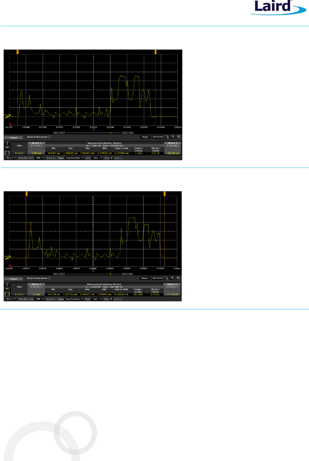
TX power: 4 dBm
Connection
29 byte payload
7.5 ms interval
Average BLE connection burst current
(excluding connection Interval): 1.67 mA
Aside:
Peak RX current: 5.95mA
Peak TX current: 8.55mA
BL652
Datasheet
Embedded Wireless Solutions Support Center:
http://ews-support.lairdtech.com
www.lairdtech.com/bluetooth
30
© Copyright 2016 Laird. All Rights Reserved
Americas: +1-800-492-2320
Europe: +44-1628-858-940
Hong Kong: +852 2923 0610
TX power: 0 dBm
Connection
29 byte payload (2.3 ms)
7.5 ms interval
Average BLE connection burst current
(excluding connection Interval): 1.56 mA
Aside:
Peak RX current: 5.92 mA
Peak TX current: 5.96 mA
TX power: -4 dBm
Connection
29 byte payload (2.3 ms)
7.5 ms interval
Average BLE connection burst current
(excluding connection Interval): 1.513
mA
Aside:
Peak RX current: 5.94 mA
Peak TX current: 4.95 mA
BL652
Datasheet
Embedded Wireless Solutions Support Center:
http://ews-support.lairdtech.com
www.lairdtech.com/bluetooth
31
© Copyright 2016 Laird. All Rights Reserved
Americas: +1-800-492-2320
Europe: +44-1628-858-940
Hong Kong: +852 2923 0610
TX power: -8 dBm
Connection
29 byte payload (2.3 ms)
7.5 ms interval
Average BLE connection burst current
(excluding connection Interval): 1.492
mA
Aside:
Peak RX current: 5.92 mA
Peak TX current: 4.58 mA
TX power: -12 dBm
Connection
29 byte payload (2.3 ms)
7.5 ms interval
Average BLE connection burst current
(excluding connection Interval):
1.488 mA
Aside:
Peak RX current: 5.93 mA
Peak TX current: 4.30 mA
BL652
Datasheet
Embedded Wireless Solutions Support Center:
http://ews-support.lairdtech.com
www.lairdtech.com/bluetooth
32
© Copyright 2016 Laird. All Rights Reserved
Americas: +1-800-492-2320
Europe: +44-1628-858-940
Hong Kong: +852 2923 0610
TX power: -16 dBm
Connection
29 byte payload (2.3 ms)
7.5 ms interval
Average BLE connection burst current
(excluding connection Interval):
1.469 mA
Aside:
Peak RX current: 5.94 mA
Peak TX current: 4.17 mA
TX power: -20 dBm
Connection
29 byte payload (2.3 ms)
7.5 ms interval
Average BLE connection burst current
(excluding connection Interval):
1.454 mA
Aside:
Peak RX current: 5.95 mA
Peak TX current: 4.03 mA
BL652
Datasheet
Embedded Wireless Solutions Support Center:
http://ews-support.lairdtech.com
www.lairdtech.com/bluetooth
33
© Copyright 2016 Laird. All Rights Reserved
Americas: +1-800-492-2320
Europe: +44-1628-858-940
Hong Kong: +852 2923 0610
TX power: -40 dBm
Connection
29 byte payload (2.3 ms)
7.5 ms interval
Average BLE connection burst current
(excluding connection Interval):
1.428 mA
Aside:
Peak RX current: 5.94 mA
Peak TX current: 3.62 mA
Peripheral Block Current Consumption
The values below are calculated for a typical operating voltage of 3V.
Table 16: UART power consumption
Parameter
Min
Typ
Max
Unit
UART Run current @ 115200 bps
-
55
-
uA
UART Run current @ 1200 bps
-
55
-
uA
Idle current for UART (no activity)
-
1
-
uA
UART Baud rate
1.2
-
1000
kbps
Table 17: power consumption
Parameter
Min
Typ
Max
Unit
SPI Master Run current @ 2 Mbps
-
50
-
uA
SPI Master Run current @ 8 Mbps
-
50
-
uA
SPI bit rate
0.125
-
8
Mbps
Table 18: I2C power consumption
Parameter
Min
Typ
Max
Unit
I2C Run current @ 100 kbps
-
50
-
uA
I2C Run current @ 400 kbps
-
50
-
uA
I2C Bit rate
100
-
400
kbps
BL652
Datasheet
Embedded Wireless Solutions Support Center:
http://ews-support.lairdtech.com
www.lairdtech.com/bluetooth
34
© Copyright 2016 Laird. All Rights Reserved
Americas: +1-800-492-2320
Europe: +44-1628-858-940
Hong Kong: +852 2923 0610
Table 19: ADC power consumption
Parameter
Min
Typ
Max
Unit
ADC current during conversion
-
700
-
uA
The above current consumption is for the given peripheral only and to operate that peripheral requires some
other internal blocks which consume base current. This base current is consumed when the UART, SPI, I2C, or
ADC is opened (operated).
For asynchronous interface like the UART (asynchronous as the other end can communicate at any time), the
UART on the BL652 must be kept open (by a command in smartBASIC application script), resulting in the base
current consumption penalty.
For a synchronous interface like the I2C or SPI (since BL652 side is the master), the interface can be closed and
opened (by a command in smartBASIC application script) only when needed, resulting in current saving (no base
current consumption penalty). There’s a similar argument for ADC (open ADC when needed).
5 FUNCTIONAL DESCRIPTION
The BL652 BLE (Bluetooth Low Energy) module is a self-contained product and requires only power and a user’s
smartBASIC application to implement full BLE functionality. The integrated, high performance antenna combined
with the RF and base-band circuitry provides the BLE wireless link, and any of the SIO lines provide the OEM’s
chosen interface connection to the sensors. The user’s smartBASIC application binds the sensors to the BLE
wireless functionality.
The variety of hardware interfaces and the smartBASIC programming language allow the BL652 module to serve
a wide range of wireless applications while reducing overall time to market and the learning curve for developing
BLE products.
To provide the widest scope for integration, a variety of physical host interfaces/sensors are provided. The major
BL652 series module functional blocks described below.
Power Management (includes Brown-out and Power on Reset)
Power management features:
System Standby Doze and Deep Sleep modes
Open/Close Peripherals (UART, SPI, I2C, SIO’s, ADC, NFC). Peripherals consume current when open; each
peripheral can be individually closed to save power consumption (with a command in a smartBASIC
application script)
Use of the internal DCDC convertor or LDO is decided by the underlying BLE stack
smartBASIC command allows the VCC voltage to be read (through the internal ADC)
Pin wake-up system from deep sleep (including from NFC pins)
Power supply features:
Supervisor hardware to manage power during reset, brownout, or power fail.
1.8V to 3.6V supply range using internal DCDC convertor or LDO decided by the underlying BLE stack.
BL652
Datasheet
Embedded Wireless Solutions Support Center:
http://ews-support.lairdtech.com
www.lairdtech.com/bluetooth
35
© Copyright 2016 Laird. All Rights Reserved
Americas: +1-800-492-2320
Europe: +44-1628-858-940
Hong Kong: +852 2923 0610
Clocks and Timers
5.2.1 Clocks
The integrated high accuracy 32 MHz (±10 ppm) crystal oscillator helps with radio operation and reducing power
consumption in the active modes.
The integrated on-chip 32.768 kHz RC oscillator (±250 ppm) provides protocol timing and helps with radio power
consumption in the system StandByDoze and Deep Sleep modes by reducing the time that the RX window needs
to be open.
To keep the on-chip 32.768 kHz RC oscillator within ±250 ppm (which is needed to run the BLE stack) accuracy,
RC oscillator needs to be calibrated (which takes 16-17 mS) regularly. The default calibration interval is eight
seconds which is enough to keep within ±250 ppm. The calibration interval ranges from 0.25 seconds to 31.75
seconds (in multiples of 0.25 seconds) and configurable via smartBASIC command at+cfg210.
5.2.2 Timers
In keeping with the event driven paradigm of smartBASIC, the timer subsystem enables smartBASIC applications
to be written which allow future events to be generated based on timeouts.
Regular Timer – There are eight built-in timers (regular timers) derived from a single RTC clock which are
controlled solely by smart BASIC functions. The resolution of the regular timer is 976 microseconds.
Tick Timer – A 31-bit free running counter that increments every (1) millisecond. The resolution of this
counter is 488 microseconds. Use the functions GetTickCount() and GetTickSince() to access this counter.
Refer to the smart BASIC User Guide available from the Laird BL652 product page.
Memory for smartBASIC Application Code
You have up to 32 kbytes of data memory available for smart BASIC application script.
Radio Frequency (RF)
2402–2480 MHz Bluetooth Low Energy radio (one Mbps over the air data rate).
Tx output power of +4 dBm programmable (via smartBASIC command) to -20 dBm in steps of 4 dB.
Tx Whisper mode1 -40 dBm (via smartBASIC command).
Receiver (with integrated channel filters) to achieve maximum sensitivity -96 dBm @ 1 Mbps BLE.
RF conducted interface available in the following two ways:
– BL652-SA: RF connected to on-board antenna on BL652-SA
– BL652-SC: RF connected to on-board IPEX MH4 RF connector on BL652-SC
Antenna options:
– Integrated monopole chip antenna on BL652-SA
– External dipole antenna connected with to IPEX MH4 RF connector on BL652-SC
NFC
NFC-A Listen mode compliant:
Based on NFC forum specification
– 13.56 MHz
BL652
Datasheet
Embedded Wireless Solutions Support Center:
http://ews-support.lairdtech.com
www.lairdtech.com/bluetooth
36
© Copyright 2016 Laird. All Rights Reserved
Americas: +1-800-492-2320
Europe: +44-1628-858-940
Hong Kong: +852 2923 0610
– Date rate 106 kbps
– NFC-A tag (can only be a target/tag; cannot be an initiator)
Modes of Operation:
– Disable
– Sense
– Activated
5.5.1 Use Cases
Touch-to Pair with NFC
Launch a smartphone app (on Android)
NFC enabled Out-of-Band Pairing
System Wake-On-Field function
– Proximity Detection
UART Interface
The Universal Asynchronous Receiver/Transmitter offers fast, full-duplex, asynchronous serial communication
with built-in flow control support (UART_CTS, UART_RTS) in HW up to one Mbps baud. Parity checking and
generation for the ninth data bit are supported.
UART_TX, UART_RX, UART_RTS, and UART_CTS form a conventional asynchronous serial data port with
handshaking. The interface is designed to operate correctly when connected to other UART devices such as the
16550A. The signaling levels are nominal 0 V and 3.3 V (tracks VCC) and are inverted with respect to the signaling
on an RS232 cable.
Two-way hardware flow control is implemented by UART_RTS and UART_CTS. UART_RTS is an output and
UART_CTS is an input. Both are active low.
These signals operate according to normal industry convention. UART_RX, UART_TX, UART_CTS, UART_RTS are
all 3.3 V level logic (tracks VCC). For example, when RX and TX are idle they sit at 3.3 V. Conversely for
handshaking pins CTS, RTS at 0 V is treated as an assertion.
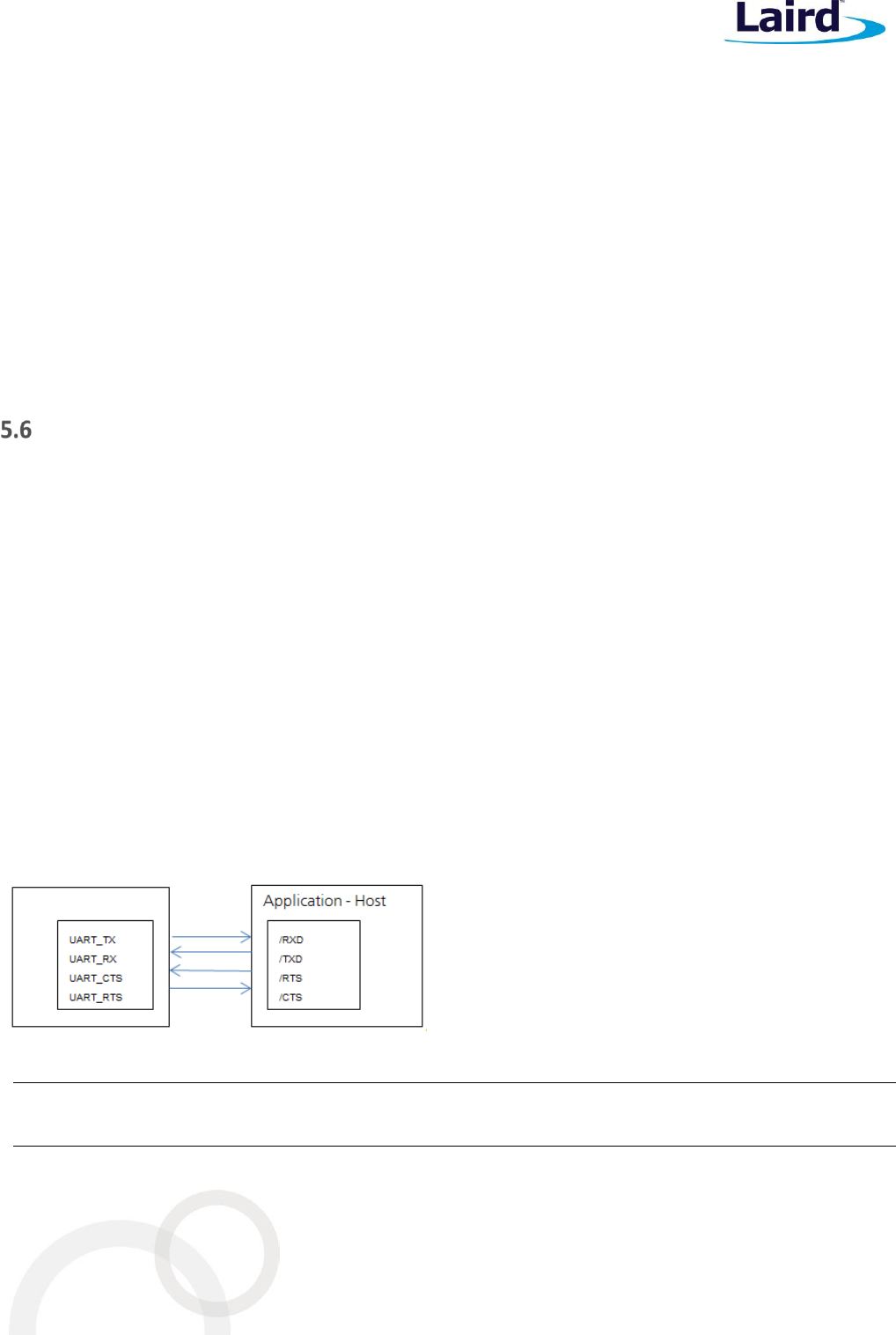
The module communicates with the customer application using the following signals:
Port/TxD of the application sends data to the module’s UART_RX signal line
Port/RxD of the application receives data from the module’s UART_TX signal line
Figure 6: UART signals
Note: The BL652 serial module output is at 3.3V CMOS logic levels (tracks VCC). Level conversion must be
added to interface with an RS-232 level compliant interface.
BL652
BL652
Datasheet
Embedded Wireless Solutions Support Center:
http://ews-support.lairdtech.com
www.lairdtech.com/bluetooth
37
© Copyright 2016 Laird. All Rights Reserved
Americas: +1-800-492-2320
Europe: +44-1628-858-940
Hong Kong: +852 2923 0610
Some serial implementations link CTS and RTS to remove the need for handshaking. We do not recommend
linking CTS and RTS other than for testing and prototyping. If these pins are linked and the host sends data at the
point that the BL652 deasserts its RTS signal, then there is significant risk that internal receive buffers will
overflow, which could lead to an internal processor crash. This will drop the connection and may require a power
cycle to reset the module. We recommend that the correct CTS/RTS handshaking protocol be adhered to for
proper operation.
Table 20: UART interface
Signal Name
Pin No
I/O
Comments
SIO_06 / UART_Tx
17
O
SIO_06 (alternative function UART_Tx) is an output, set high
(in firmware).
SIO_08 / UART_Rx
14
I
SIO_08 (alternative function UART_Rx) is an input, set with internal
pull-up (in firmware).
SIO_05 / UART_RTS
18
O
SIO_05 (alternative function UART_RTS) is an output, set low
(in firmware).
SIO_07 / UART_CTS
16
I
SIO_07 (alternative function UART_CTS) is an input, set with internal
pull-down (in firmware).
The UART interface is also used to load customer developed smartBASIC application script.
SPI Bus
The SPI interface is an alternate function on SIO pins, configurable by smartBASIC.
The module is a master device that uses terminals SPI_MOSI, SPI_MISO, and SPI_CLK. SPI_CS is implemented using
any spare SIO digital output pins to allow for multi-dropping.
The SPI interface enables full duplex synchronous communication between devices. It supports a 3-wire (SPI_MOSI,
SPI_MISO, SPI_SCK,) bidirectional bus with fast data transfers to and from multiple slaves. Individual chip select
signals are necessary for each of the slave devices attached to a bus, but control of these is left to the application
through use of SIO signals. I/O data is double-buffered.
The SPI peripheral supports SPI mode 0, 1, 2, and 3.
Table 21: SPI interfaces
Signal Name
Pin No
I/O
Comments
SPI_MOSI
3
O
This interface is an alternate function configurable by
smartBASIC. Default in the FW pin 3 and 38 are SIO inputs. SPIOPEN() in
smartBASIC selects SPI function and changes pin 3 and 38 to outputs (when in SPI
master mode).
SPI_MISO
2
I
SPI_CLK
38
O
SPI_CS
4
I
SPI_CS is implemented using any spare SIO digital output pins to allow for
multi-dropping. On Laird devboard SIO_22 (pin4) used as SPI_CS.
I2C Interface
The I2C interface is an alternate function on SIO pins, configurable by smartBASIC command.
The two-wire interface can interface a bi-directional wired-OR bus with two lines (SCL, SDA) and has master
/slave topology. The interface is capable of clock stretching. Data rates of 100 kbps and 400 kbps are supported.
BL652
Datasheet
Embedded Wireless Solutions Support Center:
http://ews-support.lairdtech.com
www.lairdtech.com/bluetooth
38
© Copyright 2016 Laird. All Rights Reserved
Americas: +1-800-492-2320
Europe: +44-1628-858-940
Hong Kong: +852 2923 0610
An I2C interface allows multiple masters and slaves to communicate over a shared wired-OR type bus consisting
of two lines which normally sit at VCC. The BL652 module can only be configured as an I2C master with additional
constraint that it be the only master on the bus. The SCL is the clock line which is always sourced by the master
and SDA is a bi-directional data line which can be driven by any device on the bus.
IMPORTANT: It is essential to remember that pull-up resistors on both SCL and SDA lines are not provided in
the module and MUST be provided external to the module.
Table 22: I2C interface
Signal Name
Pin No
I/O
Comments
I2C_SDA
37
I/O
This interface is an alternate function on each pin, configurable by
smartBASIC. I2COPEN() in smartBASIC selects I2C function.
I2C_SCL
36
I/O
General Purpose I/O, ADC, PWM and FREQ
5.9.1 GPIO
The 19 SIO pins are configurable by smartBASIC. They can be accessed individually. Each has the following user
configured features:
Input/output direction
Output drive strength (standard drive 0.5 mA or high drive 5mA)
Internal pull-up and pull-down resistors (13 K typical) or no pull-up/down
Wake-up from high or low level triggers on all pins including NFC pins
5.9.2 ADC
The ADC is an alternate function on SIO pins, configurable by smart BASIC.
The BL652 provides access to 8-channel 8/10/12-bit successive approximation ADC in one-shot mode. This
enables sampling up to 8 external signals through a front-end MUX. The ADC has configurable input and
reference pre-scaling and sample resolution (8, 10, and 12 bit).
5.9.2.1 Analog Interface (ADC)
Table 23: Analog interface
Signal Name
Pin No
I/O
Comments
AIN – Analog Input
20
I
This interface is an alternate function on each pin, configurable by
smartBASIC. AIN configuration selected using GpioSetFunc()
function.
Configurable 8, 10, 12 bit resolution.
Configurable voltage scaling 4, 2, 1/1, 1/3, 1/3, 1/4, 1/5,
1/6(default).
Configurable acquisition time 3uS, 5uS, 10uS(default), 15uS, 20uS,
40uS.
Full scale input range (VCC)
AIN – Analog Input
21
I
AIN – Analog Input
22
I
AIN – Analog Input
23
I
AIN – Analog Input
32
I
AIN – Analog Input
33
I
AIN – Analog Input
34
I
AIN – Analog Input
35
I
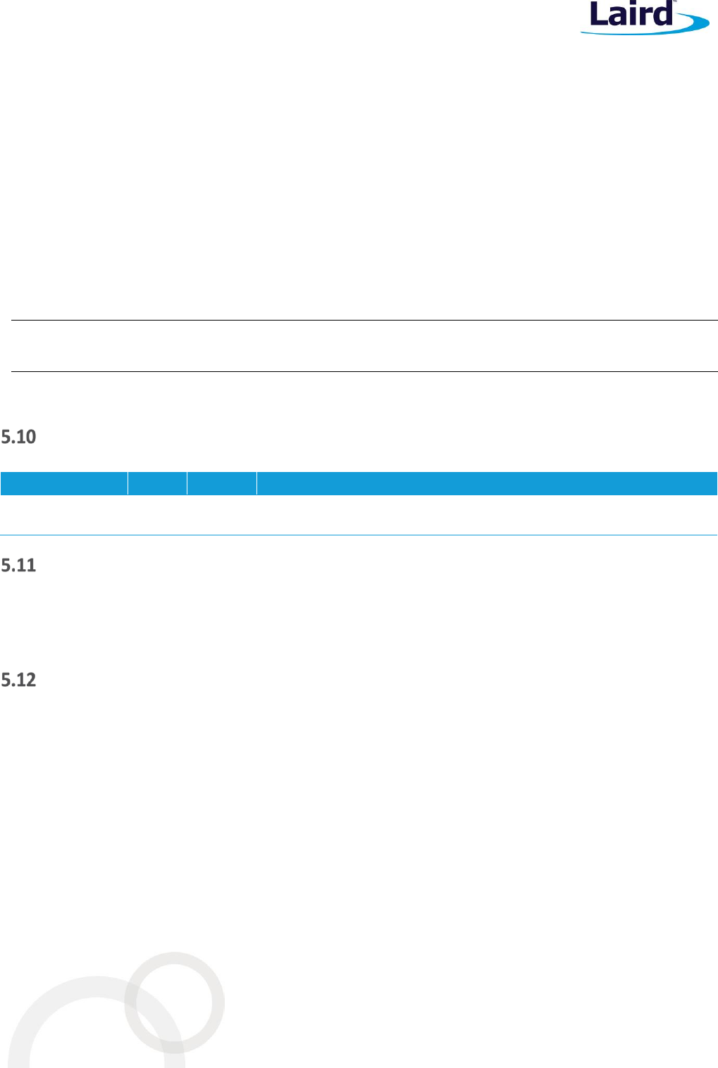
BL652
Datasheet
Embedded Wireless Solutions Support Center:
http://ews-support.lairdtech.com
www.lairdtech.com/bluetooth
39
© Copyright 2016 Laird. All Rights Reserved
Americas: +1-800-492-2320
Europe: +44-1628-858-940
Hong Kong: +852 2923 0610
5.9.3 PWM Signal Output on up to 12 SIO Pins
The PWM output is an alternate function on SIO pins, configurable by smartBASIC.
The ability to output a PWM (Pulse Width Modulated) signal on ALL GPIO (SIO) output pins can be selected using
GpioSetFunc() function.
The PWM output signal has a frequency and duty cycle property. Frequency is adjustable (up to 1MHz ) and the
duty cycle can be set over a range from 0% to 100% (both configurable by smart BASIC command).
5.9.4 FREQ Signal Output on up to 2 SIO Pins
The FREQ output is an alternate function on SIO pins, configurable by smartBASIC.
The ability to output a FREQ output signal on 2 GPIO (SIO) output pins can be selected using GpioSetFunc()
function.
Note: The frequency driving each of the two SIO pins is the same but the duty cycle can be independently
set for each pin.
FREQ output signal frequency can be set over a range of 0Hz to 4 MHz (with 50% mark-space ratio).
nRESET pin
Table 24: nRESET pin
Signal Name
Pin No
I/O
Comments
nRESET
7
I
BL652 HW reset (active low). Pull the nRESET pin low for minimum
100mS in order for the BL652 to reset.
nAutoRUN pin
Refer to nAutoRUN pin and Operating Modes regarding operating modes and the nAutoRUN pin.
Self-contained Run mode
Interactive/Development mode
vSP Command Mode
This section discusses VSP Command mode through pulling SIO_2 high and nAutoRUN low. Read this section in
conjunction with the VSP Configuration chapter of the BL652 smartBASIC Extensions Guide, found in the
documentation tab of the BL652 product page.
Figure 7 shows the difference between VSP Bridge to UART mode and VSP Command mode and how SIO_02 and
nAutoRUN must be configured to select between these two modes.
VSP Bridge to UART mode takes data sent from phone or tablet (over BLE) and sends to BL652 to be sent
out of the BL652 UART (therefore data not stored on BL652).
VSP Command mode takes data sent from phone or tablet and sends to BL652 which will interpret as an AT
command and response will be sent back. The OTA Android or iOS application can be used to download any
smartBASIC application script over the air to the BL652 because a smartBASIC application is downloaded
using AT commands.
BL652
Datasheet
Embedded Wireless Solutions Support Center:
http://ews-support.lairdtech.com
www.lairdtech.com/bluetooth
40
© Copyright 2016 Laird. All Rights Reserved
Americas: +1-800-492-2320
Europe: +44-1628-858-940
Hong Kong: +852 2923 0610
Figure 7: Differences between VSP bridge to UART mode and VSP Command mode
Table 25: vSP modes
Mode
SIO_02
nAutoRUN
VSP Bridge to UART Mode
High
High
VSP Command Mode
High
Low
SIO_02 High (externally) selects the VSP service. When SIO_02 is High and nAutoRUN is Low (externally), this
selects VSP Command mode. When SIO_12 is High and nAutoRUN is High (externally), this selects VSP Bridge to
UART mode.
When SIO_02 on module is set HIGH (externally), VSP is enabled and auto-bridged to UART when connected.
However, for VSP Command mode, auto-bridge to UART is not required. With SIO_02 set to High and nAutoRUN
set to Low, the device enters VSP Command mode and you can then download the smartBASIC application onto
the module over the air from the phone (or tablet).
Two-wire Interface JTAG
The BL652 Firmware hex file consists of four elements:
smartBASIC runtime engine
Softdevice
Master Bootloader
Laird BL652 smartBASIC firmware (FW) image part numbers are referenced as w.x.y.z (ex. v28.x.y.z). The
BL652smartBASIC runtime engine and Softdevice combined image can be upgraded by the customer over the
UART interface.
You also have the option to use the two-wire (JTAG) interface, during production, to clone the file system of a
Golden preconfigured BL652 to others using the Flash Cloning process. This is described in the app note Flash
Cloning for the BL652. In this case the file system is also part of the .hex file.
Signal Name
Pin No
I/O
Comments
SWDIO
5
I/O
Internal pull-up resistor
SWDCLK
6
I
Internal pull-down resistor
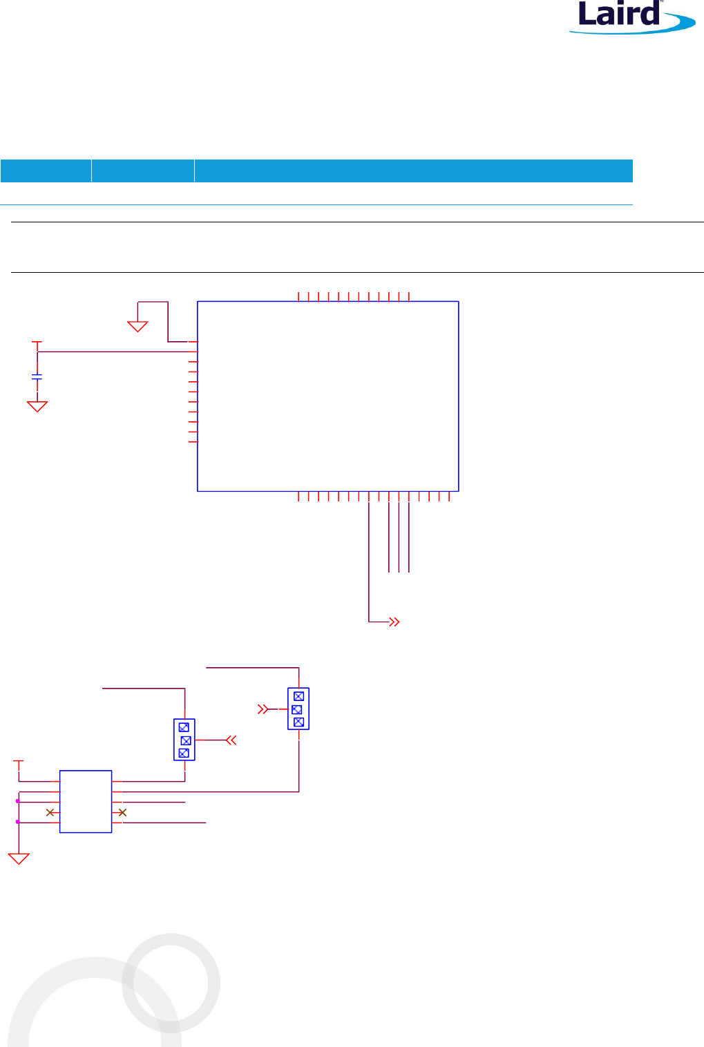
BL652
Datasheet
Embedded Wireless Solutions Support Center:
http://ews-support.lairdtech.com
www.lairdtech.com/bluetooth
41
© Copyright 2016 Laird. All Rights Reserved
Americas: +1-800-492-2320
Europe: +44-1628-858-940
Hong Kong: +852 2923 0610
The Laird DVK-BL652 development board incorporates an on-board JTAG J-link programmer for this purpose.
There is also the following JTAG connector which allows on-board JTAG J-link programmer signals to be routed
off the development board. The only requirement is that you should use the following JTAG connector on the
host PCB.
The JTAG connector MPN is as follows:
Reference
Part
Description and MPN (Manufacturers Part Number)
JP1
FTSH-105
Header, 1.27mm, SMD, 10-way, FTSH-105-01-L-DV Samtech
Note: Reference on the BL652 development board schematic (Figure 8) shows the DVK-BL652-xx
development schematic wiring only for the JTAG connector and the BL652 module JTAG pins.
Figure 8: BL652 development board schematic
SIO_18
U5
CON_SM_39
GND
1
SIO_23/SPI_MOSI
3
SIO_17 30
SIO_15 29
SIO_13/nAutoRUN 28
SIO_22
4
GND
27
NFC2/SIO_10
14 NFC1/SIO_09
15
SIO_25/SPI_CLK 38
nRESET
7
VDD_nRF
26
SIO_16/SFLASH_CLK
10
SIO_24/SPI_MISO
2
GND
16
SWDIO
5SWDCLK
6
SIO_20/SFLASH_MOSI
8SIO_18
9
SIO_14/SFLASH_MISO
11 SIO_12/SFLASH_CS
12 SIO_11
13
SIO_08/UART_RX
17 SIO_07/UART_CTS
18 SIO_06/UART_TX
19 SIO_05/UART_RTS/AIN3
20 SIO_04/AIN2
21 SIO_03/AIN1
22 SIO_02/AIN0
23 SIO_01/XL2
24 SIO_00/XL1
25
SIO_19 31
SIO_31/AIN7 32
SIO_30/AIN6 33
SIO_29/AIN5 34
SIO_28/AIN4 35
SIO_27/I2C_SCL 36
SIO_26/I2C_SDA 37
GND 39
GND
SWDIO_BLE
VCC_BLE
SIO_18
SWDCLK_BLE
VCC_BLE
nRESET_BLE
C9
0.1uF,16V
GND
GND
SWDIO
VCC_IO
SWDCLK
JP1
NOPOP (PIN HEADER,1.27mm 2X5P)
1 2
3 4
5 6
7 8
910
PIN HEADER,2.54mm 1X3P
J3
11
22
3
3
PIN HEADER,2.54mm 1X3P
J4
11
2
2
3
3
SWDCLK_BLE
nRESET_BLE
SIO_18
SWDIO_BLE
BL652
Datasheet
Embedded Wireless Solutions Support Center:
http://ews-support.lairdtech.com
www.lairdtech.com/bluetooth
42
© Copyright 2016 Laird. All Rights Reserved
Americas: +1-800-492-2320
Europe: +44-1628-858-940
Hong Kong: +852 2923 0610
Note: J3 and J4 (on the DVK-BL652-xx development board allows Laird on-board JTAG J-link programmer
signals to be routed off the development board by fitting jumpers in the J3 pins (2-3) and J4 pins (2-3).
BL652 Wakeup
5.14.1 Waking Up BL652 from Host
Wake the BL652 from the host using wake-up pins (any SIO pin). Refer to the smartBASIC user guide for details.
You may configure the BL652’s wakeup pins via smartBASIC to do any of the following:
Wake up when signal is low
Wake up when signal is high
Wake up when signal changes
Refer to the smartBASIC user guide for details. You can access this guide from the Laird BL652 product page.
Low Power Modes
The BL652 has three power modes: Run, Standby Doze, and Deep Sleep.
The module is placed automatically in Standby Doze if there are no pending events (when WAITEVENT statement
is encountered within a customer’s smartBASIC script). The module wakes from Standby Doze via any interrupt
(such as a received character on the UART Rx line). If the module receives a UART character from either the
external UART or the radio, it wakes up.
Deep sleep is the lowest power mode. Once awakened, the system goes through a system reset.
Temperature Sensor
The on-silicon temperature sensor has a temperature range greater than or equal to the operating temperature
of the device. Resolution is 0.25 degrees.
To read temperature from on-silicon temperature sensor (in tenth of centigrade, so 23.4°C is output as 234):
In command mode, use ATI2024
or
From running from a running smartBASIC application script, use SYSINFO(2024)
Random Number Generator
Exposed via an API in smartBASIC (see smartBASIC documentation available from the BL652 product page).
The rand() function from a running smartBASIC application returns a value.
AES Encryption/Decryption
Exposed via an API in smartBASIC (see smartBASIC documentation available from the BL652 product page).
Function called aesencrypt and aesdecrypt.
BL652
Datasheet
Embedded Wireless Solutions Support Center:
http://ews-support.lairdtech.com
www.lairdtech.com/bluetooth
43
© Copyright 2016 Laird. All Rights Reserved
Americas: +1-800-492-2320
Europe: +44-1628-858-940
Hong Kong: +852 2923 0610
Optional External Serial (SPI) Flash
This is not required for normal BL652 module opertion.
If you fit an optional external serial (SPI) flash (such as for data logging purpose) then that external serial (SPI)
flash must connect to BL652 module pins SIO_12 (SFLASH_CS), SIO_14 (SFLASH_MISO), SIO_16 (SFLASH_CLK),
and SIO_20 (SFLASH_MOSI); in that case a high level API in smartBASIC can be used for fast access using
open/close /read/write API functions.
Note: By default, these are GPIO pins. Only when in their FlashOpen()smartBASIC app are these lines
dedicated to SPI and for talking to the off-module board SPI flash.
If you decide to use external serial (SPI) flash with the BL652-SX-xx, then ONLY the manufacturer part numbers
below MUST be used:
4-Mbit Macronix MX25R4035F
http://www.macronix.com/Lists/DataSheet/Attachments/3288/MX25R4035F,%20Wide%20Range,%204Mb,
%20v1.2.pdf
8-Mbit Macronix MX25R8035F
http://www.macronix.com/Lists/DataSheet/Attachments/3532/MX25R8035F,%20Wide%20Range,%208Mb,
%20v1.2.pdf
For any external serial (SPI) flash other than these part numbers, smartBASIC does not provide access.
Optional External 32.768 kHz crystal
This is not required for normal BL652 module operation.
The BL652 uses the on-chip 32.76 kHz RC oscillator (LFCLK) by default (which has an accuracy of ±250 ppm) which
requires regulator calibration (every eight seconds) to within ±250 ppm.
You can connect an optional external high accuracy (±20 ppm) 32.768 kHz crystal to the BL652-SX-xx pins,
SIO_01/XL2 (pin 24) and SIO_00/XL1 (pin 25) to provide improved protocol timing and to help with radio power
consumption in the system standby doze/deep sleep modes by reducing the time that the RX window needs to
be open. Table 26 compares the current consumption difference between RC and crystal oscillator.
Table 26: Comparing current consumption difference between BL652 on-chip RC 32.76 kHz oscillator and optional external crystal
(32.768kHz) based oscillator
BL652 On-chip 32.768 kHz RC Oscillator
(±250 ppm) LFRC
Optional External Higher Accuracy (±20 ppm)
32.768 kHz Crystal-based Oscillator XO
Current
Consumption
of 32.768 kHz
Block
0.6 uA
0.25 uA
Standby Doze
Current
1.2 uA
1.2 uA
BL652
Datasheet
Embedded Wireless Solutions Support Center:
http://ews-support.lairdtech.com
www.lairdtech.com/bluetooth
44
© Copyright 2016 Laird. All Rights Reserved
Americas: +1-800-492-2320
Europe: +44-1628-858-940
Hong Kong: +852 2923 0610
BL652 On-chip 32.768 kHz RC Oscillator
(±250 ppm) LFRC
Optional External Higher Accuracy (±20 ppm)
32.768 kHz Crystal-based Oscillator XO
Calibration
Calibration required regularly (default eight
seconds interval)
Calibration takes 16-17 ms; with DCDC used,
the total charge of a calibration event is 7.4 uC.
The average current consumed by the
calibration depends on the calibration interval
and can be calculated using the following
formula:
CAL_charge/CAL_interval
The lowest calibration interval (0.25 seconds)
provides an average current of (DCDC
enabled):
7.4uC / 0.25s = 29.6uA
To get the 250 ppm accuracy, the BLE stack
specification states that a calibration interval
of eight seconds is enough. This gives an
average current of:
7.4uC / 8s = 0.93 uA
Added to the LFRC run current and Standby
Doze (IDLE) base current shown above results
in a total average current of:
LFRC + CAL = 1.8 + 0.93 = 2.7uA
Not applicable
Total
2.7 uA
1.45 uA
Summary
Low current consumption
Accuracy 250 ppm
Lowest current consumption
Needs external crystal
High accuracy (depends on the crystal, usually
20 ppm)
Table 27: Optional external 32.768 kHz crystal specification
Optional external 32.768kHz crystal
Min
Typ
Max
Crystal Frequency
-
32.768 kHz
-
Frequency tolerance requirement of BLE stack
-
-
±250 ppm
Load Capacitance
-
-
12.5 pF
Shunt Capacitance
-
-
2 pF
Equivalent series resistance
-
-
100 kOhm
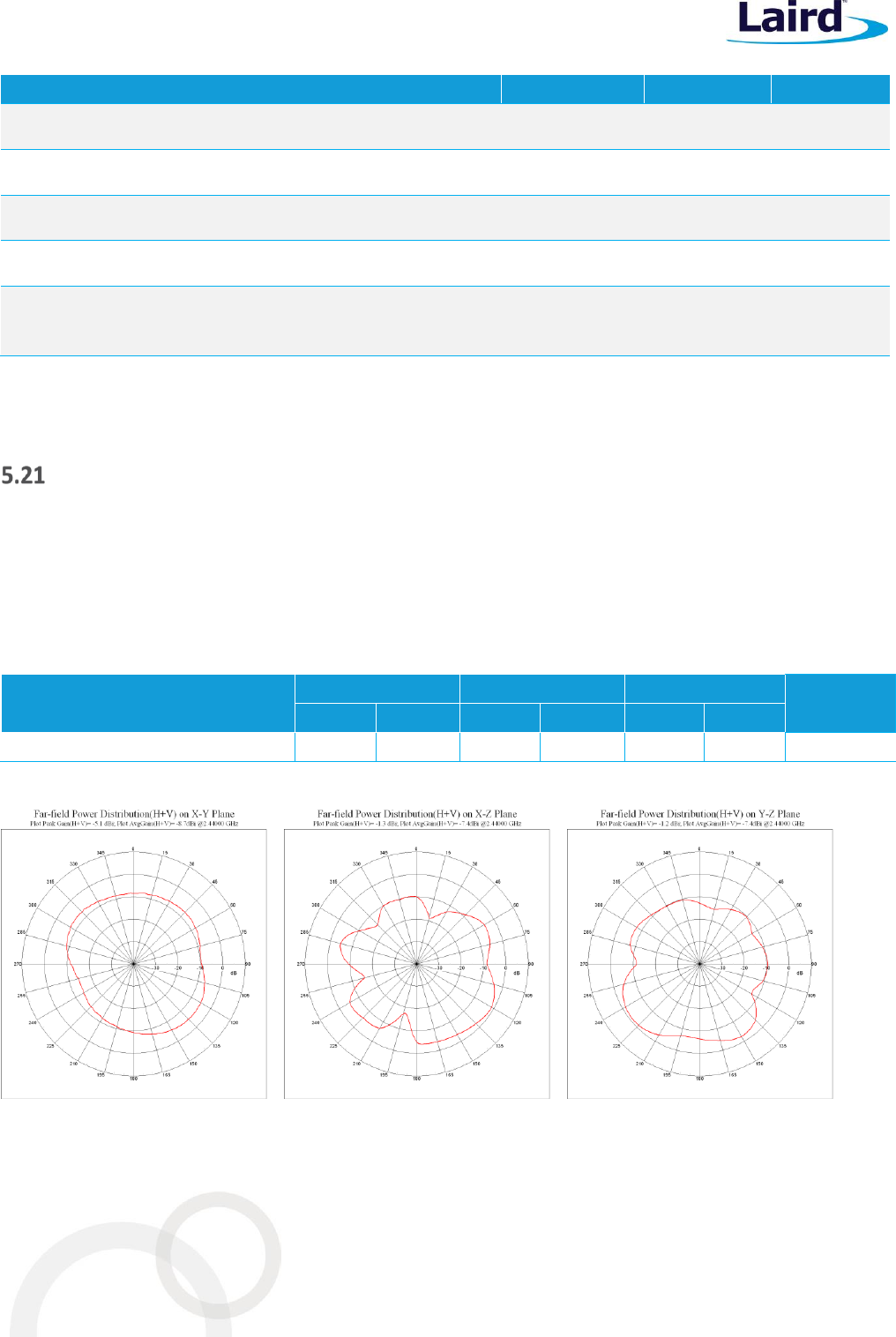
BL652
Datasheet
Embedded Wireless Solutions Support Center:
http://ews-support.lairdtech.com
www.lairdtech.com/bluetooth
45
© Copyright 2016 Laird. All Rights Reserved
Americas: +1-800-492-2320
Europe: +44-1628-858-940
Hong Kong: +852 2923 0610
Optional external 32.768kHz crystal
Min
Typ
Max
Drive level
-
-
1 uW
Input capacitance on XL1 and XL2 pads
-
4 pF
-
Run current for 32.768 kHz crystal based oscillator
-
0.25 uA
-
Startup time for 32.768 kHz crystal based oscillator
-
0.25 seconds
-
Peak to peak amplitude for external low swing clock input
signal must not be outside supply rails
200 mV
-
1000 mV
Be sure to tune the load capacitors on the board design to optimize frequency accuracy (at room temperature) so
it matches that of the same crystal standalone, Drive Level (so crystal operated within safe limits) oscillation
margin (Rneg is at least 3 to 5 times ESR) over the operating temperature range.
BL652-SA On-board Chip Antenna Characteristics
The BL652-SA on-board chip monopole antenna radiated performance depends on the host PCB layout.
The BL652 development board was used for BL652 development and antenna performance evaluation. To obtain
similar performance, follow guidelines in section PCB Layout on Host PCB for BL652-SA to allow the on-board
antenna to radiate and reduce proximity effects due to nearby host PCB GND copper or metal covers.
BL652-SA on-board chip antenna datasheet: http://www.acxc.com.tw/product/at/at3216/AT3216-B2R7HAA_S-
R00-N198_2.pdf
Unit in dBi @2.44GHz
XY-plane
XZ-plane
YZ-plane
Efficiency
Peak
Avg
Peak
Avg
Peak
Avg
AT3216-B2R7HAA
-5.1
-8.7
-1.3
-7.4
-5.1
-8.7
25.0%
◆XY-plane ◆XZ-plane ◆YZ-plane
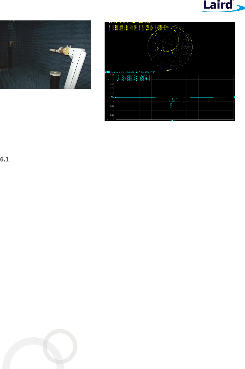
BL652
Datasheet
Embedded Wireless Solutions Support Center:
http://ews-support.lairdtech.com
www.lairdtech.com/bluetooth
46
© Copyright 2016 Laird. All Rights Reserved
Americas: +1-800-492-2320
Europe: +44-1628-858-940
Hong Kong: +852 2923 0610
6 HARDWARE INTEGRATION SUGGESTIONS
Circuit
The BL652 is easy to integrate, requiring no external components on your board apart from those which you
require for development and in your end application.
The following are suggestions for your design for the best performance and functionality.
Checklist (for Schematic):
VCC pins
External power source should be within the operating range, rise time and noise/ripple specification of the
BL652. Add decoupling capacitors for filtering the external source. Power-on reset circuitry within BL652
series module incorporates brown-out detector, thus simplifying your power supply design. Upon
application of power, the internal power-on reset ensures that the module starts correctly.
VCC and coin-cell operation
With built-in DCDC (operating range 1.7V to 3.6V), reduces the peak current required from a coin-cell
(CR2032), making it easier to use with coin-cell.
AIN (ADC) and SIO pin IO voltage levels
BL652 SIO voltage levels are at VCC. Ensure input voltage levels into SIO pins are at VCC also (if VCC source is
a battery whose voltage will drop). Ensure ADC pin maximum input voltage for damage is not violated.
AIN (ADC) impedance and external voltage divider setup
If you need to measure with ADC a voltage higher than 3.6V, you can connect a high impedance voltage
divider to lower the voltage to the ADC input pin.
JTAG
This is not required as smartBASIC runtime engine firmware can be loaded using the UART. JTAG may be
used if you intend to use Flash Cloning during production to load smartBASIC scripts.
Table 28: BL652-SA on-board chip antenna performance (Antenna Gain, efficiency and S11 (whilst BL652-SA-xx module on DVK-
BL652-xx development board)

BL652
Datasheet
Embedded Wireless Solutions Support Center:
http://ews-support.lairdtech.com
www.lairdtech.com/bluetooth
47
© Copyright 2016 Laird. All Rights Reserved
Americas: +1-800-492-2320
Europe: +44-1628-858-940
Hong Kong: +852 2923 0610
UART
Required for loading your smartBASIC application script during development (or for subsequent firmware
upgrades (except JTAG for FW upgrades and/or Flash Cloning of the smartBASIC application script). Add
connector to allow interfacing with UART via PC (UART–RS232 or UART-USB).
UART_RX and UART_CTS
SIO_8 (alternative function UART_RX) is an input, set with internal weak pull-up (in firmware). The pull-up
prevents the module from going into deep sleep when UART_RX line is idling.
SIO_7 (alternative function UART_CTS) is an input, set with internal weak pull-down (in firmware). This pull-
down ensures the default state of the UART_CTS will be asserted which means can send data out of the
UART_TX line. Laird recommends that UART_CTS be connected.
nAutoRUN pin and operating mode selection
nAutoRUN pin needs to be externally held high or low to select between the two BL652 operating modes at
power-up:
– Self-contained Run mode (nAutoRUN pin held at 0V).
– Interactive / development mode (nAutoRUN pin held at VCC).
Make provision to allow operation in the required mode. Add jumper to allow nAutoRUN pin to be
held high or low (BL652 has internal 13K pull-down by default) OR driven by host GPIO.
I2C
It is essential to remember that pull-up resistors on both I2C_SCL and I2C_SDA lines are not provided in the
BL652 module and MUST be provided external to the module as per I2C standard.
SPI
Implement SPI chip select using any unused SIO pin within your smartBASIC application script then SPI_CS is
controlled from smartBASIC application allowing multi-dropping.
SIO pin direction
BL652 modules shipped from production with smart BASIC runtime engine FW, all SIO pins (with default
function of DIO) are mostly digital inputs (see Pin Definitions Table2). Remember to change the direction SIO
pin (in your smart BASIC application script) if that particular pin is wired to a device that expects to be driven
by the BL652 SIO pin configured as an output. Also, these SIO pins have the internal pull-up or pull-down
resistor-enabled by default in firmware (see Pin Definitions Table 2). This was done to avoid floating inputs,
which can cause current consumption in low power modes (e.g. StandbyDoze) to drift with time. You can
disable the PULL-UP or Pull-down through their smartBASIC application.
Note: Internal pull-up, pull down will take current from VCC.
SIO_02 pin and OTA smartBASIC application download feature
SIO_02 is an input, set with internal pull-down (in FW). Refer to latest firmware release documentation on
how SIO_02 is used for Over the Air smartBASIC application download feature. SIO_02 pin has to be pulled
high externally to enable the feature. Decide if this feature is required in production. When SIO_02 is high,
ensure nAutoRun is NOT high at same time; otherwise you cannot load the smartBASIC application script.
NFC antenna connector
To make use of the Laird flexi-PCB NFC antenna, fit connector:
Description: FFC/FPC Connector, Right Angle, SMD/90d,Dual Contact,1.2mm Mated Height
Manufacturer: Molex
Manufacturers Part number: 512810594
BL652
Datasheet
Embedded Wireless Solutions Support Center:
http://ews-support.lairdtech.com
www.lairdtech.com/bluetooth
48
© Copyright 2016 Laird. All Rights Reserved
Americas: +1-800-492-2320
Europe: +44-1628-858-940
Hong Kong: +852 2923 0610
Add tuning capacitors of 300 pF on NGC1 pin to GND and 300 pF on NFC2 pins to GND if the PCB track length
is similar as DVK-BL652 devboard.
nRESET pin (active low)
Hardware reset. Wire out to push button or drive by host.
By default module is out of reset when power applied to VCC pins.
Optional External 32.768kHz crystal
If the optional external 32.768kHz crystal is needed then use a crystal that meets specification.
Optional External serial SPI flash IC
If the optional external serial (SPI) flash is required, ensure that manufacturer part number tested by Laird
are used.
PCB Layout on Host PCB - General
Checklist (for PCB):
MUST locate BL652-Sx module close to the edge of PCB (mandatory for BL652-SA for on-board chip antenna
to radiate properly).
Use solid GND plane on inner layer (for best EMC and RF performance).
All module GND pins MUST be connected to host PCB GND.
Place GND vias close to module GND pads as possible.
Unused PCB area on surface layer can flooded with copper but place GND vias regularly to connect copper
flood to inner GND plane. If GND flood copper underside the module then connect with GND vias to inner
GND plane.
Route traces to avoid noise being picked up on VCC supply and AIN (analogue) and SIO (digital) traces.
Ensure no exposed copper is on the underside of the module (refer to land pattern of BL652 development
board).
PCB Layout on Host PCB for BL652-SA
6.3.1 Antenna Keep-out on Host PCB
The BL652-SA has an integrated chip antenna and its performance is sensitive to host PCB. It is critical to locate
the BL652-SA on the edge of the host PCB (or corner) to allow the antenna to radiate properly. Refer to
guidelines in section PCB land pattern and antenna keep-out area for BL652-SA. Some of those guidelines
repeated below.
Ensure there is no copper in the antenna keep-out area on any layers of the host PCB. Keep all mounting
hardware and metal clear of the area to allow proper antenna radiation.
For best antenna performance, place the BL652-SA module on the edge of the host PCB, preferably in the
corner with the antenna facing the corner.
The BL652 development board has the BL652-SA module on the edge of the board (not in the corner). The
antenna keep-out area is defined by the BL652 development board which was used for module
development and antenna performance evaluation is shown in Figure 9, where the antenna keep-out area is
~4.95mm wide, 25.65 mm long; with PCB dielectric (no copper) height 0.85 mm sitting under the BL652-SA
antenna.
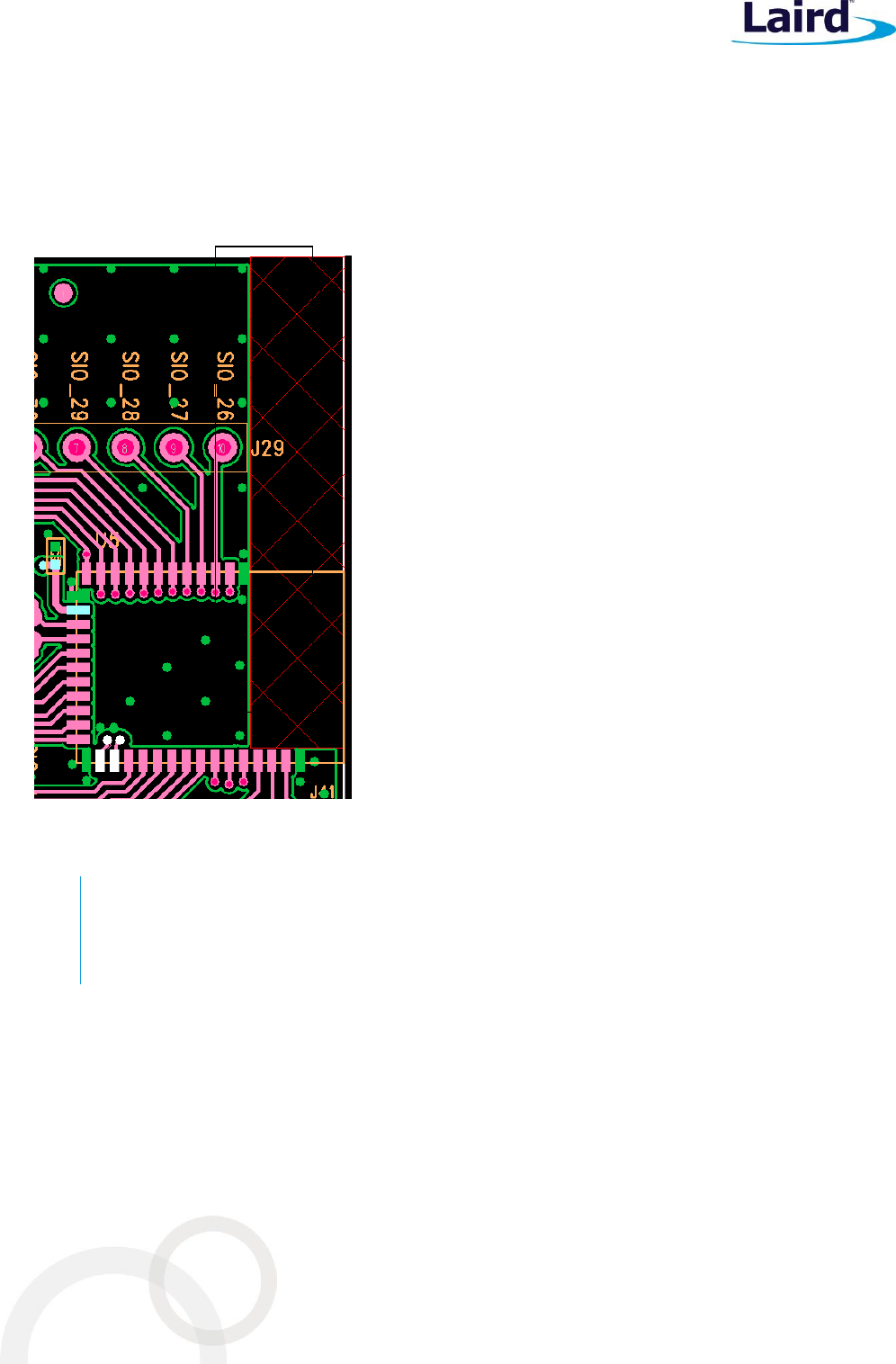
BL652
Datasheet
Embedded Wireless Solutions Support Center:
http://ews-support.lairdtech.com
www.lairdtech.com/bluetooth
49
© Copyright 2016 Laird. All Rights Reserved
Americas: +1-800-492-2320
Europe: +44-1628-858-940
Hong Kong: +852 2923 0610
The BL652-SA antenna is tuned when BL652-SA is sitting on development board (host PCB) with size of 120
mm x 93 mm.
A different host PCB thickness dielectric will have small effect on antenna.
The antenna-keep-out defined in the Host PCB Land Pattern and Antenna Keep-out for BL652-SA section.
Host PCB land pattern and antenna keep-out for the BL652 applies when the BL652-SA is placed in the
corner of the host PCB. When BL652-SA cannot be placed as such, it must be placed on the edge of the host
PCB and the antenna keep out must be observed. Figure 9 shows an example.
Figure 9: Antenna keep-out area (shown in red), corner of the BL652 development board for BL652-SA module.
Antenna Keep-out Notes:
Note 1
The BL652 module is placed on the edge of the host PCB.
Note 2
Copper cut-away on all layers in the Antenna Keep-out area under BL652 on host PCB.
6.3.2 Antenna Keep-out and Proximity to Metal or Plastic
Checklist (for metal /plastic enclosure):
Minimum safe distance for metals without seriously compromising the antenna (tuning) is 40 mm
top/bottom and 30 mm left or right.
Metal close to the BL652-SA chip monopole antenna (bottom, top, left, right, any direction) will have
degradation on the antenna performance. The amount of that degradation is entirely system dependent,
meaning you will need to perform some testing with your host application.
BL652-SA module
Antenna Keep-out
BL652
Datasheet
Embedded Wireless Solutions Support Center:
http://ews-support.lairdtech.com
www.lairdtech.com/bluetooth
50
© Copyright 2016 Laird. All Rights Reserved
Americas: +1-800-492-2320
Europe: +44-1628-858-940
Hong Kong: +852 2923 0610
Any metal closer than 20 mm will begin to significantly degrade performance (S11, gain, radiation
efficiency).
It is best that you test the range with a mock-up (or actual prototype) of the product to assess effects of
enclosure height (and materials, whether metal or plastic).
External Antenna Integration with BL652-SC
Please refer to the regulatory sections for FCC, IC, CE, and Japan for details of use of BL652-Sx with external
antennas in each regulatory region.
The BL652 family has been designed to operate with the below external antennas (with a maximum gain of
2.0 dBi). The required antenna impedance is 50 ohms. See Table 29. External antennas improve radiation
efficiency.
Table 29: External antennas for the BL652
External Antenna
Part Number
Laird Part
Number
Mfg.
Type
Gain
(dBi)
Connector Type
BL652 Part
Number
FlexPIFA (001-0022)
LSR
PCB
Dipole
2.0
IPEX-4
(See Note 1)
BL652-SC
FlexNotch (001-0023)
LSR
PCB
Dipole
2.0
IPEX-4
(See Note 1)
BL652-SC
EDA-8709-2G4C1-B27-CY
Mag.Layers
Dipole
2.0
IPEX-4
(See Note 1)
BL652-SC
RFDPA870910EMAB302
0600-00057
Walsin
Dipole
2.0
IPEX-4
(See Note 1)
BL652-SC
Note 1: Integral RF co-axial cable (1.13 mm OD) with length 100±5 mm and IPEX-4 compatible connector.
These antennas are available through Laird – please contact Sales for information.
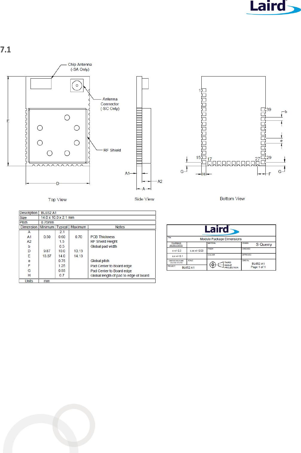
BL652
Datasheet
Embedded Wireless Solutions Support Center:
http://ews-support.lairdtech.com
www.lairdtech.com/bluetooth
51
© Copyright 2016 Laird. All Rights Reserved
Americas: +1-800-492-2320
Europe: +44-1628-858-940
Hong Kong: +852 2923 0610
7 MECHANICAL DETAILS
BL652 Mechanical Details
Figure 10: BL652 mechanical drawings
Development Kit Schematics can be found in the software downloads tab of the BL652 product page:
http://www.lairdtech.com/Products/BL652-Series
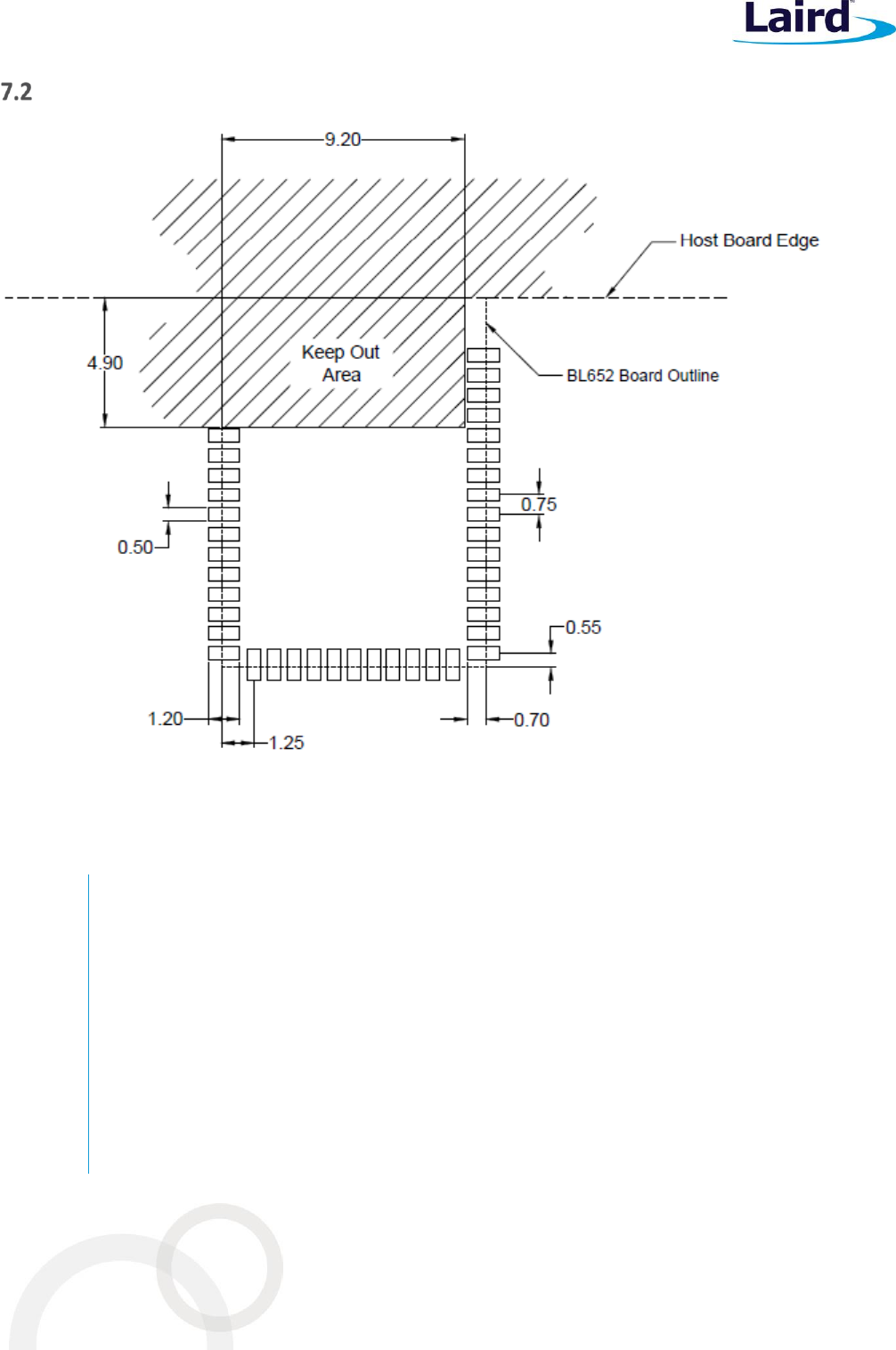
BL652
Datasheet
Embedded Wireless Solutions Support Center:
http://ews-support.lairdtech.com
www.lairdtech.com/bluetooth
52
© Copyright 2016 Laird. All Rights Reserved
Americas: +1-800-492-2320
Europe: +44-1628-858-940
Hong Kong: +852 2923 0610
Host PCB Land Pattern and Antenna Keep-out for BL652-SA
Figure 11: Land pattern and Keep-out for BL652-SA
All dimensions are in mm.
Host PCB Land Pattern and Antenna Keep-out for BL652-SANotes:
Note 1
Ensure there is no copper in the antenna ‘keep out area’ on any layers of the host PCB. Also keep all
mounting hardware or any metal clear of the area (Refer to 6.3.2) to reduce effects of proximity
detuning the antenna and to help antenna radiate properly.
Note 2
For the best on-board antenna performance, the module BL652-SA MUST be placed on the edge of
the host PCB and preferably in the corner with the antenna facing the corner. Above “Keep Out
Area” is the module placed in corner of PCB. If BL652-SA is not placed in corner but on edge of host
PCB, the antenna “Keep Out Area” is extended (see Note 4).
Note 3
BL652 development board has BL652-SA placed on the edge of the PCB board (and not in corner) for
that the Antenna keep out area is extended down to the corner of the development board, see
section PCB Layout on Host PCB for BL652-SA, Figure 11. This was used for module development and
antenna performance evaluation.
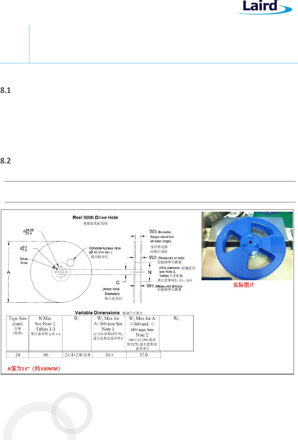
BL652
Datasheet
Embedded Wireless Solutions Support Center:
http://ews-support.lairdtech.com
www.lairdtech.com/bluetooth
53
© Copyright 2016 Laird. All Rights Reserved
Americas: +1-800-492-2320
Europe: +44-1628-858-940
Hong Kong: +852 2923 0610
Note 4
Ensure that there is no exposed copper under the module on the host PCB.
Note 5
You may modify the PCB land pattern dimensions based on their experience and/or process
capability.
8 APPLICATION NOTE FOR SURFACE MOUNT MODULES
Introduction
Laird Technologies surface mount modules are designed to conform to all major manufacturing guidelines. This
application note is intended to provide additional guidance beyond the information that is presented in the User
Manual. This Application Note is considered a living document and will be updated as new information is
presented.
The modules are designed to meet the needs of a number of commercial and industrial applications. They are
easy to manufacture and conform to current automated manufacturing processes.
Shipping
8.2.1 Tape and Reel Package Information
Note: Ordering information for tape and reel packaging involves the addition of T/R to the end of the full
module part number. For example, BL652-SA-0x becomes BL652-SA-0x-T/R.
Figure 12: Reel specifications
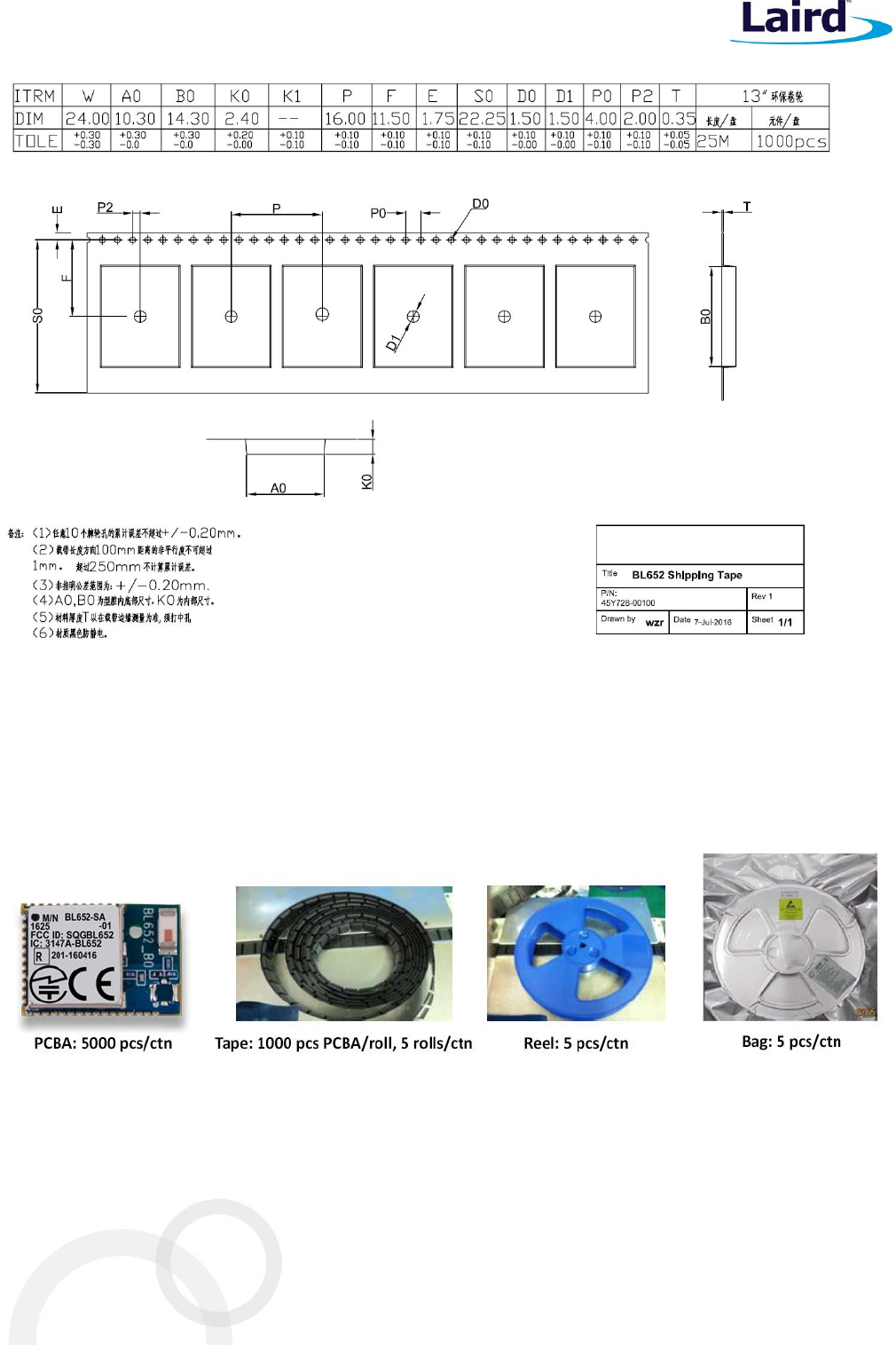
BL652
Datasheet
Embedded Wireless Solutions Support Center:
http://ews-support.lairdtech.com
www.lairdtech.com/bluetooth
54
© Copyright 2016 Laird. All Rights Reserved
Americas: +1-800-492-2320
Europe: +44-1628-858-940
Hong Kong: +852 2923 0610
Figure 13: Tape specifications
There are 1000 BL652 modules taped in a reel (and packaged in a pizza box) and five boxes per carton (5000
modules per carton). Reel, boxes, and carton are labeled with the appropriate labels. See Carton Contents for
more information.
8.2.2 Carton Contents
The following are the contents of the carton shipped for the BL652 modules.
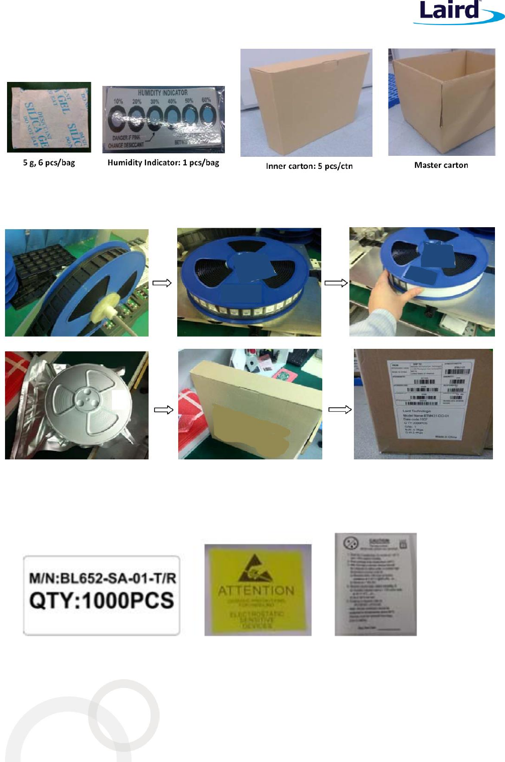
BL652
Datasheet
Embedded Wireless Solutions Support Center:
http://ews-support.lairdtech.com
www.lairdtech.com/bluetooth
55
© Copyright 2016 Laird. All Rights Reserved
Americas: +1-800-492-2320
Europe: +44-1628-858-940
Hong Kong: +852 2923 0610
8.2.3 Packaging Process
Figure 15: BL652 packaging process
8.2.4 Labeling
The following labels are located on the antistatic bag:
Figure 16: Antistatic bag labels
Figure 14: Carton contents for the BL652
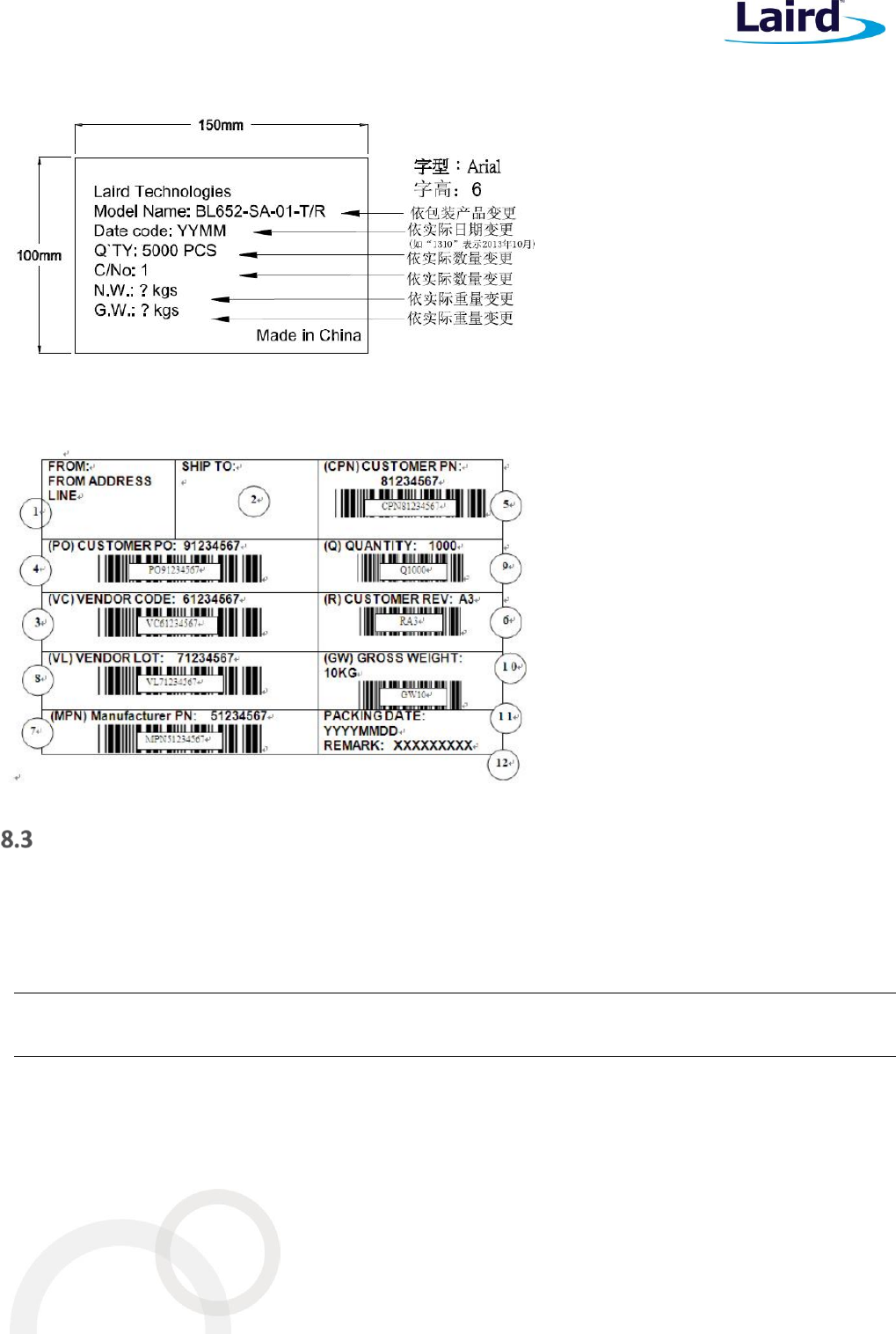
BL652
Datasheet
Embedded Wireless Solutions Support Center:
http://ews-support.lairdtech.com
www.lairdtech.com/bluetooth
56
© Copyright 2016 Laird. All Rights Reserved
Americas: +1-800-492-2320
Europe: +44-1628-858-940
Hong Kong: +852 2923 0610
The following package label is located on both sides of the master carton:
Figure 17: Master carton package label
The following is the packing slip label:
Figure 18: Packing slip label
Reflow Parameters
Prior to any reflow, it is important to ensure the modules were packaged to prevent moisture absorption. New
packages contain desiccate (to absorb moisture) and a humidity indicator card to display the level maintained
during storage and shipment. If directed to bake units on the card, see Table 30 and follow instructions specified
by IPC/JEDEC J-STD-033. A copy of this standard is available from the JEDEC website:
http://www.jedec.org/sites/default/files/docs/jstd033b01.pdf
Note: The shipping tray cannot be heated above 65°C. If baking is required at the higher temperatures
displayed in in Table 30, the modules must be removed from the shipping tray.
Any modules not manufactured before exceeding their floor life should be re-packaged with fresh desiccate and
a new humidity indicator card. Floor life for MSL (Moisture Sensitivity Level) 3 devices is 168 hours in ambient
environment 30°C/60%RH.
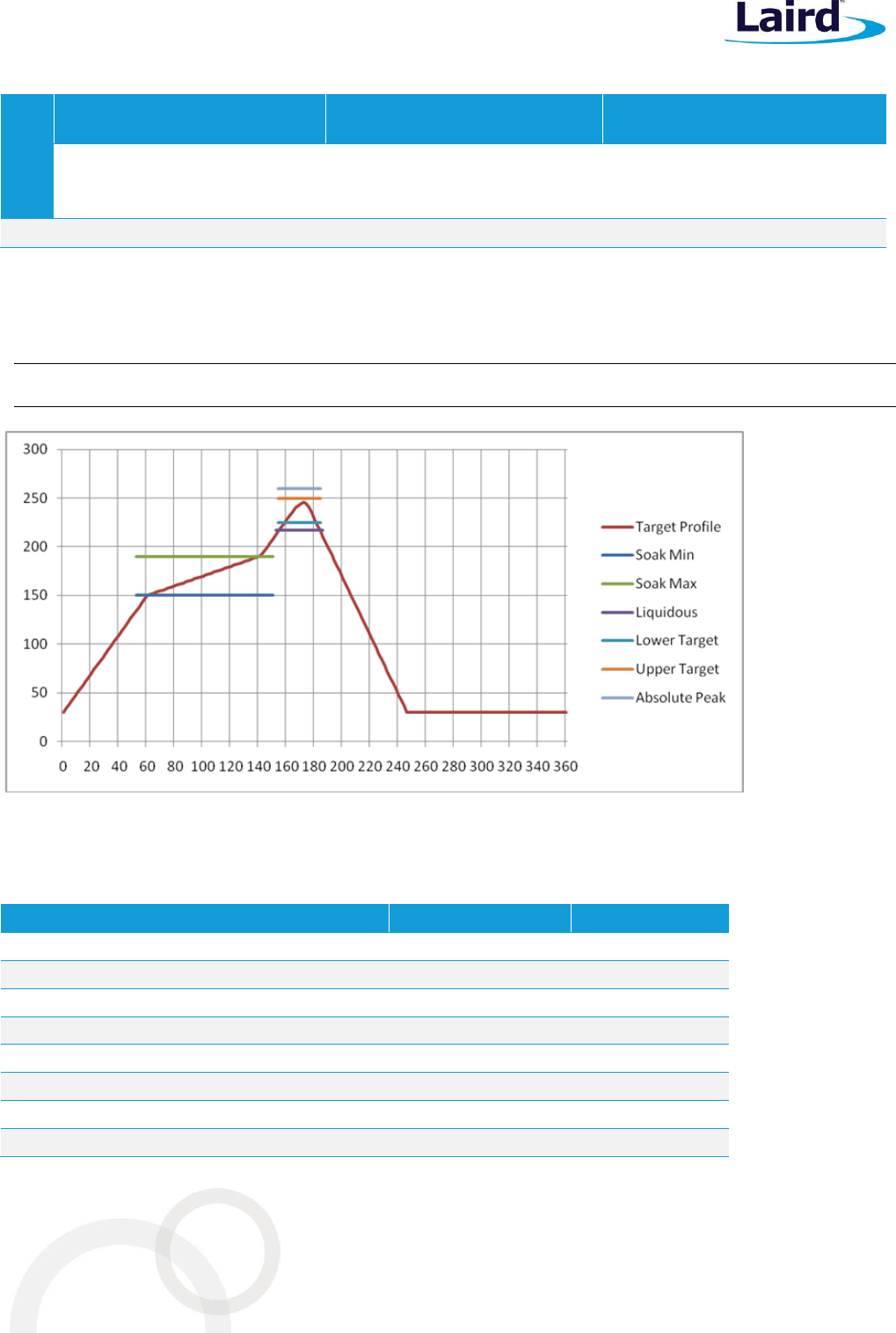
BL652
Datasheet
Embedded Wireless Solutions Support Center:
http://ews-support.lairdtech.com
www.lairdtech.com/bluetooth
57
© Copyright 2016 Laird. All Rights Reserved
Americas: +1-800-492-2320
Europe: +44-1628-858-940
Hong Kong: +852 2923 0610
Table 30: Recommended baking times and temperatures
MSL
125°C
Baking Temp.
90°C/≤ 5%RH
Baking Temp.
40°C/ ≤ 5%RH
Baking Temp.
Saturated
@
30°C/85%
Floor Life Limit
+ 72 hours
@ 30°C/60%
Saturated
@
30°C/85%
Floor Life Limit
+ 72 hours
@ 30°C/60%
Saturated
@
30°C/85%
Floor Life Limit
+ 72 hours @
30°C/60%
3
9 hours
7 hours
33 hours
23 hours
13 days
9 days
Laird surface mount modules are designed to be easily manufactured, including reflow soldering to a PCB.
Ultimately it is the responsibility of the customer to choose the appropriate solder paste and to ensure oven
temperatures during reflow meet the requirements of the solder paste. Laird surface mount modules conform to
J-STD-020D1 standards for reflow temperatures.
Important: During reflow, modules should not be above 260° and not for more than 30 seconds.
Figure 19: Recommended reflow temperature
Temperatures should not exceed the minimums or maximums presented in Table 31.
Table 31: Recommended maximum and minimum temperatures
Specification
Value
Unit
Temperature Inc./Dec. Rate (max)
1~3
°C / Sec
Temperature Decrease rate (goal)
2-4
°C / Sec
Soak Temp Increase rate (goal)
.5 - 1
°C / Sec
Flux Soak Period (Min)
70
Sec
Flux Soak Period (Max)
120
Sec
Flux Soak Temp (Min)
150
°C
Flux Soak Temp (max)
190
°C
Time Above Liquidous (max)
70
Sec
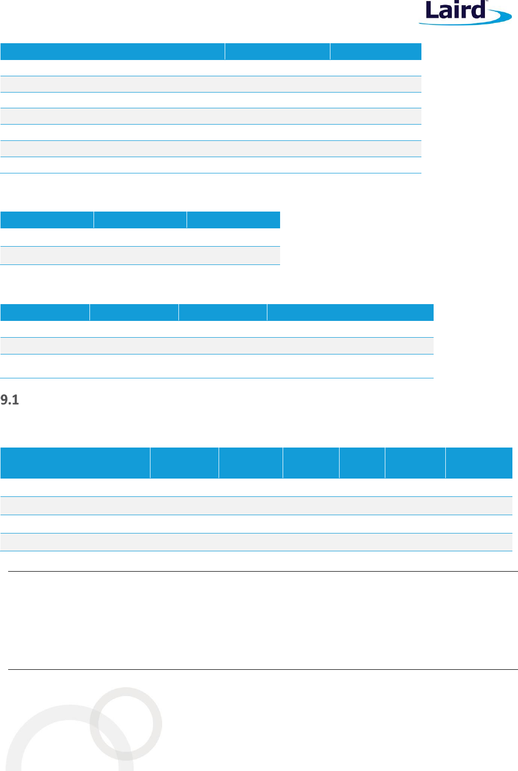
BL652
Datasheet
Embedded Wireless Solutions Support Center:
http://ews-support.lairdtech.com
www.lairdtech.com/bluetooth
58
© Copyright 2016 Laird. All Rights Reserved
Americas: +1-800-492-2320
Europe: +44-1628-858-940
Hong Kong: +852 2923 0610
Specification
Value
Unit
Time Above Liquidous (min)
50
Sec
Time In Target Reflow Range (goal)
30
Sec
Time At Absolute Peak (max)
5
Sec
Liquidous Temperature (SAC305)
218
°C
Lower Target Reflow Temperature
240
°C
Upper Target Reflow Temperature
250
°C
Absolute Peak Temperature
260
°C
9 FCC AND IC REGULATORY STATEMENTS
Model
US/FCC
Canada/IC
BL652-SA
SQGBL652
3147A-BL652
BL652-SC
SQGBL652
3147A-BL652
The BL652SA and BL652-SC hold full modular approvals. The OEM must follow the regulatory guidelines and
warnings listed below to inherit the modular approval.
Part #
Form Factor
Tx Outputs
Antenna
BL652-SA-SA
Surface Mount
4 dBm
Ceramic
BL652-SC-SC
Surface Mount
4 dBm
IPEX MHF4
*Last two slots "XX" in Part # are used for production firmware release changes. Can be values 01-99, aa-zz
Antenna Information
The BL652 family has been designed to operate with the antennas listed below with a maximum gain of 2.21 dBi.
The required antenna impedance is 50 ohms.
External Antenna Part Number
Laird Part
Number
Mfg.
Type
Gain
(dBi)
Connector
Type
BL652 Part
number
FlexPIFA
001-0022
LSR
PCB Dipole
2.0
IPEX-4
BL652-SC
FlexNotch
001-0023
LSR
PCB Dipole
2.0
IPEX-4
BL652-SC
EDA-8709-2G4C1-B27-CY
Mag.Layers
Dipole
2.0
IPEX-4
BL652-SC
RFDPA870910EMAB302
0600-00057
Walsin
Dipole
2.0
IPEX-4
BL652-SC
Note: The OEM is free to choose another vendor’s antenna of like type and equal or lesser gain as an
antenna appearing in the table and still maintain compliance. Reference FCC Part 15.204(c)(4) for
further information on this topic.
To reduce potential radio interference to other users, the antenna type and gain should be chosen so
that the equivalent isotropic radiated power (EIRP) is not more than that permitted for successful
communication.
BL652
Datasheet
Embedded Wireless Solutions Support Center:
http://ews-support.lairdtech.com
www.lairdtech.com/bluetooth
59
© Copyright 2016 Laird. All Rights Reserved
Americas: +1-800-492-2320
Europe: +44-1628-858-940
Hong Kong: +852 2923 0610
Power Exposure Information
Federal Communication Commission (FCC) Radiation Exposure Statement:
This EUT is in compliance with SAR for general population/uncontrolled exposure limits in ANSI/IEEE C95.1-1999
and had been tested in accordance with the measurement methods and procedures specified in OET Bulletin 65
Supplement C.
This transceiver must not be co-located or operating in conjunction with any other antenna, transmitter, or
external amplifiers. Further testing / evaluation of the end product will be required if the OEM’s device violates
any of these requirements.
The BL652 is fully approved for mobile and portable applications.
OEM Responsibilities
WARNING: The OEM must ensure that FCC labelling requirements are met. This includes a clearly visible label
on the outside of the OEM enclosure specifying the appropriate Laird Technology FCC identifier
for this product.
Contains FCC ID: SQGBL652 IC: 3147A-BL652
If the size of the end product is larger than 8x10cm, then the following FCC part 15.19 statement
has to also be available on visible on outside of device:
The enclosed device complies with Part 15 of the FCC Rules. Operation is subject to the following
two conditions: (1) This device may not cause harmful interference, and (2) This device must
accept any interference received, including interference that may cause undesired operation
Label and text information should be in a size of type large enough to be readily legible, consistent with the
dimensions of the equipment and the label. However, the type size for the text is not required to be larger than
eight point.
CAUTION: The OEM should have their device which incorporates the BL652 tested by a qualified test house to
verify compliance with FCC Part 15 Subpart B limits for unintentional radiators.
CAUTION: Any changes or modifications not expressly approved by Laird Technology could void the user’s
authority to operate the equipment.
Federal Communication Commission Interference Statement
This equipment has been tested and found to comply with the limits for a Class B digital device, pursuant to Part
15 of the FCC Rules. These limits are designed to provide reasonable protection against harmful interference in a
residential installation. This equipment generates, uses and can radiate radio frequency energy and, if not
installed and used in accordance with the instructions, may cause harmful interference to radio communications.
However, there is no guarantee that interference will not occur in a particular installation. If this equipment does
cause harmful interference to radio or television reception, which can be determined by turning the equipment
off and on, the user is encouraged to try to correct the interference by one of the following measures:
Reorient or relocate the receiving antenna.
Increase the separation between the equipment and receiver.

BL652
Datasheet
Embedded Wireless Solutions Support Center:
http://ews-support.lairdtech.com
www.lairdtech.com/bluetooth
60
© Copyright 2016 Laird. All Rights Reserved
Americas: +1-800-492-2320
Europe: +44-1628-858-940
Hong Kong: +852 2923 0610
Connect the equipment into an outlet on a circuit different from that to which the receiver is connected.
Consult the dealer or an experienced radio/TV technician for help.
FCC Caution: Any changes or modifications not expressly approved by the party responsible for compliance could
void the user's authority to operate this equipment.
This device complies with Part 15 of the FCC Rules. Operation is subject to the following two conditions: (1) This
device may not cause harmful interference, and (2) this device must accept any interference received, including
interference that may cause undesired operation.
IMPORTANT NOTE:
FCC Radiation Exposure Statement:
The product comply with the US portable RF exposure limit set forth for an uncontrolled environment and are
safe for intended operation as described in this manual. The further RF exposure reduction can be achieved if
the product can be kept as far as possible from the user body or set the device to lower output power if such
function is available.
This transmitter must not be co-located or operating in conjunction with any other antenna or transmitter.
This device is intended only for OEM integrators under the following conditions:
(1) The transmitter module may not be co-located with any other transmitter or antenna,
As long as the condition above is met, further transmitter test will not be required. However, the OEM
integrator is still responsible for testing their end-product for any additional compliance requirements required
with this module installed
IMPORTANT NOTE
In the event that these conditions can not be met (for example certain laptop configurations or co-location with
another transmitter), then the FCC authorization is no longer considered valid and the FCC ID can not be used on
the final product. In these circumstances, the OEM integrator will be responsible for re-evaluating the end
product (including the transmitter) and obtaining a separate FCC authorization.
End Product Labeling
The final end product must be labeled in a visible area with the following: “Contains FCC ID: SQGBL652”.
Manual Information to the End User
The OEM integrator has to be aware not to provide information to the end user regarding how to install or
remove this RF module in the user’s manual of the end product which integrates this module.
The end user manual shall include all required regulatory information/warning as show in this manual.
Industry Canada Statement
This device complies with Industry Canada’s license-exempt RSSs. Operation is subject to the following two
conditions:
(1) This device may not cause interference; and

BL652
Datasheet
Embedded Wireless Solutions Support Center:
http://ews-support.lairdtech.com
www.lairdtech.com/bluetooth
61
© Copyright 2016 Laird. All Rights Reserved
Americas: +1-800-492-2320
Europe: +44-1628-858-940
Hong Kong: +852 2923 0610
(2) This device must accept any interference, including interference that may cause undesired operation of the
device.
Le présent appareil est conforme aux CNR d’Industrie Canada applicables aux appareils radio exempts de
licence. L’exploitation est autorisée aux deux conditions suivantes:
(1) l’appareil ne doit pas produire de brouillage;
(2) l’utilisateur de l’appareil doit accepter tout brouillage radioélectrique subi, même si le brouillage est
susceptible d’en compromettre le fonctionnement.
Radiation Exposure Statement
The product comply with the Canada portable RF exposure limit set forth for an uncontrolled environment and
are safe for intended operation as described in this manual. The further RF exposure reduction can be achieved
if the product can be kept as far as possible from the user body or set the device to lower output power if such
function is available.
Déclaration d'exposition aux radiations:
Le produit est conforme aux limites d'exposition pour les appareils portables RF pour les Etats-Unis et le Canada
établies pour un environnement non contrôlé. Le produit est sûr pour un fonctionnement tel que décrit dans ce
manuel. La réduction aux expositions RF peut être augmentée si l'appareil peut être conservé aussi loin que
possible du corps de l'utilisateur ou que le dispositif est réglé sur la puissance de sortie la plus faible si une telle
fonction est disponible.
This device is intended only for OEM integrators under the following conditions:
(1) The transmitter module may not be co-located with any other transmitter or antenna.
As long as 1 condition above are met, further transmitter test will not be required. However, the OEM integrator
is still responsible for testing their end-product for any additional compliance requirements required with this
module installed.
Cet appareil est conçu uniquement pour les intégrateurs OEM dans les conditions suivantes:
(1) Le module émetteur peut ne pas être coïmplanté avec un autre émetteur ou antenne.
Tant que les 1 condition ci-dessus sont remplies, des essais supplémentaires sur l'émetteur ne seront pas
nécessaires. Toutefois, l'intégrateur OEM est toujours responsable des essais sur son produit final pour toutes
exigences de conformité supplémentaires requis pour ce module installé.
IMPORTANT NOTE:
In the event that these conditions can not be met (for example certain laptop configurations or co-location with
another transmitter), then the Canada authorization is no longer considered valid and the IC ID can not be used
on the final product. In these circumstances, the OEM integrator will be responsible for re-evaluating the end
product (including the transmitter) and obtaining a separate Canada authorization.
NOTE IMPORTANTE:
Dans le cas où ces conditions ne peuvent être satisfaites (par exemple pour certaines configurations
d'ordinateur portable ou de certaines co-localisation avec un autre émetteur), l'autorisation du Canada n'est
plus considéré comme valide et l'ID IC ne peut pas être utilisé sur le produit final. Dans ces circonstances,
BL652
Datasheet
Embedded Wireless Solutions Support Center:
http://ews-support.lairdtech.com
www.lairdtech.com/bluetooth
62
© Copyright 2016 Laird. All Rights Reserved
Americas: +1-800-492-2320
Europe: +44-1628-858-940
Hong Kong: +852 2923 0610
l'intégrateur OEM sera chargé de réévaluer le produit final (y compris l'émetteur) et l'obtention d'une
autorisation distincte au Canada.
End Product Labeling
The final end product must be labeled in a visible area with the following: “Contains IC: 3147A-BL652”.
Plaque signalétique du produit final
Le produit final doit être étiqueté dans un endroit visible avec l'inscription suivante: "Contient des IC: 3147A-
BL652".
Manual Information to the End User
The OEM integrator has to be aware not to provide information to the end user regarding how to install or
remove this RF module in the user’s manual of the end product which integrates this module.
The end user manual shall include all required regulatory information/warning as show in this manual.
Manuel d'information à l'utilisateur final
L'intégrateur OEM doit être conscient de ne pas fournir des informations à l'utilisateur final quant à la façon
d'installer ou de supprimer ce module RF dans le manuel de l'utilisateur du produit final qui intègre ce module.
Le manuel de l'utilisateur final doit inclure toutes les informations réglementaires requises et avertissements
comme indiqué dans ce manuel.
10 JAPAN (MIC) REGULATORY
The BL652 is approved for use in the Japanese market. The part numbers listed below hold WW type
certification. Refer to ARIB-STD-T66 for further guidance on OEM’s responsibilities.
Model
Certificate Number
Antenna
BL652-SA
201-160415
Ceramic
BL652-SC
201-160416
IPEX MHF4
Antenna Information
The BL652 was tested with antennas listed below. The OEM can choose a different manufacturers antenna but
must make sure it is of same type and that the gain is lesser than or equal to the antenna that is approved for
use.
External Antenna Part Number
Laird Part
Number
Mfg.
Type
Gain
(dBi)
Connector
Type
BL652 Part
Number
FlexPIFA
001-0022
LSR
PCB
Dipole
2.0
IPEX-4
BL652-SC
FlexNotch
001-0023
LSR
PCB
Dipole
2.0
IPEX-4
BL652-SC
EDA-8709-2G4C1-B27-CY
Mag.Layers
Dipole
2.0
IPEX-4
BL652-SC
RFDPA870910EMAB302
0600-00057
Walsin
Dipole
2.0
IPEX-4
BL652-SC
BL652
Datasheet
Embedded Wireless Solutions Support Center:
http://ews-support.lairdtech.com
www.lairdtech.com/bluetooth
63
© Copyright 2016 Laird. All Rights Reserved
Americas: +1-800-492-2320
Europe: +44-1628-858-940
Hong Kong: +852 2923 0610
11 CE REGULATORY
The BL652-SA/BL652-SC have been tested for compliance with relevant standards for the EU market. The BL652-
SC module was tested with a 2.21 dBi antenna. The OEM can operate the BL652-SC module with any other type
of antenna but must ensure that the gain does not exceed 2.21 dBi to maintain the Laird approval.
The OEM should consult with a qualified test house before entering their device into an EU member country to
make sure all regulatory requirements have been met for their complete device.
Reference the Declaration of Conformities listed below for a full list of the standards that the modules were
tested to. Test reports are available upon request.
Antenna Information
The antennas listed below were tested for use with the BL652. For CE mark countries, the OEM is free to use any
manufacturer’s antenna and type of antenna as long as the gain is less than or equal to the highest gain approved
for use (2.21dBi) Contact a Laird representative for more information regarding adding antennas.
External Antenna Part Number
Laird Part
Number
Mfg.
Type
Gain
(dBi)
Connector
Type
BL652 Part
number
FlexPIFA
001-0022
LSR
PCB
Dipole
2.0
IPEX-4
BL652-SC
FlexNotch
001-0023
LSR
PCB
Dipole
2.0
IPEX-4
BL652-SC
EDA-8709-2G4C1-B27-CY
Mag.Layers
Dipole
2.0
IPEX-4
BL652-SC
RFDPA870910EMAB302
0600-00057
Walsin
Dipole
2.0
IPEX-4
BL652-SC
Note: The BL652 module internal BLE chipset IC pins are rated 4 kV (ESD HBM). ESD can find its way through
the external JTAG connector (if used on the customers design), if discharge is applied directly.
Customer should ensure adequate protection against ESD on their end product design (using the
BL652 module) to meet relevant ESD standard (for CE, this is EN301-489).
BL652
Datasheet
Embedded Wireless Solutions Support Center:
http://ews-support.lairdtech.com
www.lairdtech.com/bluetooth
64
© Copyright 2016 Laird. All Rights Reserved
Americas: +1-800-492-2320
Europe: +44-1628-858-940
Hong Kong: +852 2923 0610
12 EU DECLARATIONS OF CONFORMITY
BL652-SA/BL652-SC
Manufacturer:
Laird
Product:
BL652-SA, BL652-SC
EU Directive:
RTTE 1995/5/EC
Conformity Assessment:
Annex IV
Reference standards used for presumption of conformity:
Article Number
Requirement
Reference standard(s)
3.1a
Health and Safety
EN60950-1:2006+A11:2009+A1:2010+A12:2011
3.1b
Protection requirements with
respect to electromagnetic
compatibility
EN 301 489-1 V1.9.2 (2011-09)
EN 301 489-17 V2.2.1 (2012-09)
Emissions:
EN55022:2006/A1:2007 (Class B)
Immunity:
EN61000-4-2:2009
EN61000-4-3:2006/A1:2008/A2:2010
3.2
Means of the efficient use of
the radio frequency spectrum
EN 300 328 V1.8.1 (2012-06)
Declaration:
We, Laird, declare under our sole responsibility that the essential radio test suites have been carried out and that
the above product to which this declaration relates is in conformity with all the applicable essential requirements
of Article 3 of the EU Directive 1999/5/EC, when used for its intended purpose.
Place of Issue:
Laird
Saturn House, Mercury Park
Wooburn Green
HP100HH, United Kingdom
tel: +44 (0)1628 858 940
fax: +44 (0)1628 528 382
Date of Issue:
Name of Authorized Person:
Signature:
BL652
Datasheet
Embedded Wireless Solutions Support Center:
http://ews-support.lairdtech.com
www.lairdtech.com/bluetooth
65
© Copyright 2016 Laird. All Rights Reserved
Americas: +1-800-492-2320
Europe: +44-1628-858-940
Hong Kong: +852 2923 0610
13 ORDERING INFORMATION
BL652-SA-0x
Intelligent BTv4.2 Module featuring smartBASIC (internal antenna)
BL652-SC-0x
Intelligent BTv4.2 Module featuring smartBASIC (IPEX MHF4 connector)
DVK-BL652-SA / SC-0x
Development Kit for each BL652 series module above
General Comments
This is a preliminary datasheet. Please check with Laird for the latest information before commencing a design. If
in doubt, ask.
14 BLUETOOTH SIG QUALIFICATION
Overview
The BL652 module is listed on the Bluetooth SIG website as a qualified End Product.
Design
Name
Owner
Declaration ID
QD ID
Link to listing on the SIG website
BL652
Laird
D031950
87158
TBD
It is a mandatory requirement of the Bluetooth Special Interest Group (SIG) that every product implementing
Bluetooth technology has a Declaration ID. Every Bluetooth design is required to go through the qualification
process, even when referencing a Bluetooth Design that already has its own Declaration ID. The Qualification
Process requires each company to register as a member of the Bluetooth SIG – www.bluetooth.org
The following is a link to the Bluetooth Registration page: https://www.bluetooth.org/login/register/
For each Bluetooth Design it is necessary to purchase a Declaration ID. This can be done before starting the new
qualification, either through invoicing or credit card payment. The fees for the Declaration ID will depend on your
membership status, please refer to the following webpage:
https://www.bluetooth.org/en-us/test-qualification/qualification-overview/fees
For a detailed procedure of how to obtain a new Declaration ID for your design, please refer to the following SIG
document:
https://www.bluetooth.org/DocMan/handlers/DownloadDoc.ashx?doc_id=283698&vId=317486
Qualification Steps When Referencing a Laird End Product Design
To qualify your product when referencing a Laird end-product design, follow these steps:
1. To start a listing, go to: https://www.bluetooth.org/tpg/QLI_SDoc.cfm
Note: A user name and password are required to access this site.
2. In step 1, select the option, New Listing and Reference a Qualified Design.
BL652
Datasheet
Embedded Wireless Solutions Support Center:
http://ews-support.lairdtech.com
www.lairdtech.com/bluetooth
66
© Copyright 2016 Laird. All Rights Reserved
Americas: +1-800-492-2320
Europe: +44-1628-858-940
Hong Kong: +852 2923 0610
3. Enter TBD or TBD in the End Product table entry.
4. Select your pre-paid Declaration ID from the drop down menu or go to the Purchase Declaration ID page.
Note: Unless the Declaration ID is pre-paid or purchased with a credit card, you cannot proceed until the SIG
invoice is paid.
5. Once all the relevant sections of step 1 are finished, complete steps 2, 3, and 4 as described in the help
document accessible from the site.
Your new design will be listed on the SIG website and you can print your Certificate and DoC.
For further information please refer to the following training material:
https://www.bluetooth.org/en-us/test-qualification/qualification-overview/listing-process-updates
Note: If using the BL652 with Laird Firmware and smartBASIC script, you can skip Controller Subsystem, Host
Subsystem, and Profile Subsystem.
Qualification Steps When Deviating from a Laird End Product Design
If you wish to deviate from the standard End Product designs listed under TBD or TBD, the qualification process
follows the New Listing route (without referencing a Qualified Design). When creating a new design it is
necessary to complete the full qualification listing process and also maintain a compliance folder for the design.
If your design is based on un-modified BL652 hardware, follow these steps:
1. Reference the existing RF-PHY test report from the BL600 listing.
Note: This report is available from Laird: ews-support@lairdtech.com
2. Combine the relevant Nordic Link Layer (LL).
3. Combine in a Host Component (covering L2CAP, GAP, ATT, GATT, SM).
4. Test any standard SIG profiles that are supported in the design, (customs
profiles are exempt).
The first step is to generate a project on the TPG (Test Plan Generator) system, select
‘Traditional Project’. This determines which test cases apply to demonstrate
compliance with the Bluetooth Test Specifications, from the TPG you generate a Test
Declaration, (Excel format). If you are combining pre-tested and qualified
components in your design, and they are within their 3 year listing period, you are
not required to re-test those layers covered by those components.
Figure 20: Scope of the qualification for an End Product Design.
End
Product
Laird RF-PHY
Nordic LL
Host
Layers
Profiles
BL652
Datasheet
Embedded Wireless Solutions Support Center:
http://ews-support.lairdtech.com
www.lairdtech.com/bluetooth
67
© Copyright 2016 Laird. All Rights Reserved
Americas: +1-800-492-2320
Europe: +44-1628-858-940
Hong Kong: +852 2923 0610
Examples of LL components that can be combined into a new design are:
Listing reference
Design Name
Core Spec Version
TBD
S130_nRF51xxx link layer
4.2
*Note: Please check with Laird/Nordic for applicable LL components.
Examples of Host Stack components that can be integrated into the new design are;
Listing reference
Design Name
Core Spec Version
TBD
S130_nRF51xxx host layer
4.2
*Note: You may choose any Host Stack and optional profiles in you design.
If the design incorporates any standard SIG LE profiles (such as Heart Rate Profile, refer to section, External to the
Core - Current and Qualifiable GATT-based Profile and Service Test Requirements), it is necessary to test these
profiles using PTS or other tools where permitted; the results are added to the compliance folder.
You are required to upload your test declaration and test reports (where applicable) and complete the final
listing steps on the SIG website. Remember to purchase your Declaration ID before you start the qualification
process; you cannot complete the listing without it.
To start a listing, go to: https://www.bluetooth.org/tpg/QLI_SDoc.cfm. In step 1, select the option, New Listing,
(without referencing a Qualified Design).
Additional Assistance
Please contact your local sales representative or our support team for further assistance:
Laird Technologies Connectivity Products Business Unit
Support Centre: http://ews-support.lairdtech.com
Email: wireless.support@lairdtech.com
Phone: Americas: +1-800-492-2320
Europe: +44-1628-858-940
Hong Kong: +852 2923 0610
Web: http://www.lairdtech.com/bluetooth
© Copyright 2016 Laird. All Rights Reserved. Patent pending. Any information furnished by Laird and its agents is believed to be accurate and reliable. All
specifications are subject to change without notice. Responsibility for the use and application of Laird materials or products rests with the end user since
Laird and its agents cannot be aware of all potential uses. Laird makes no warranties as to non-infringement nor as to the fitness, merchantability, or
sustainability of any Laird materials or products for any specific or general uses. Laird, Laird Technologies, Inc., or any of its affiliates or agents shall not be
liable for incidental or consequential damages of any kind. All Laird products are sold pursuant to the Laird Terms and Conditions of Sale in effect from time
to time, a copy of which will be furnished upon request. When used as a tradename herein, Laird means Laird PLC or one or more subsidiaries of Laird PLC.
Laird™, Laird Technologies™, corresponding logos, and other marks are trademarks or registered trademarks of Laird. Other marks may be the property of
third parties. Nothing herein provides a license under any Laird or any third party intellectual property right.