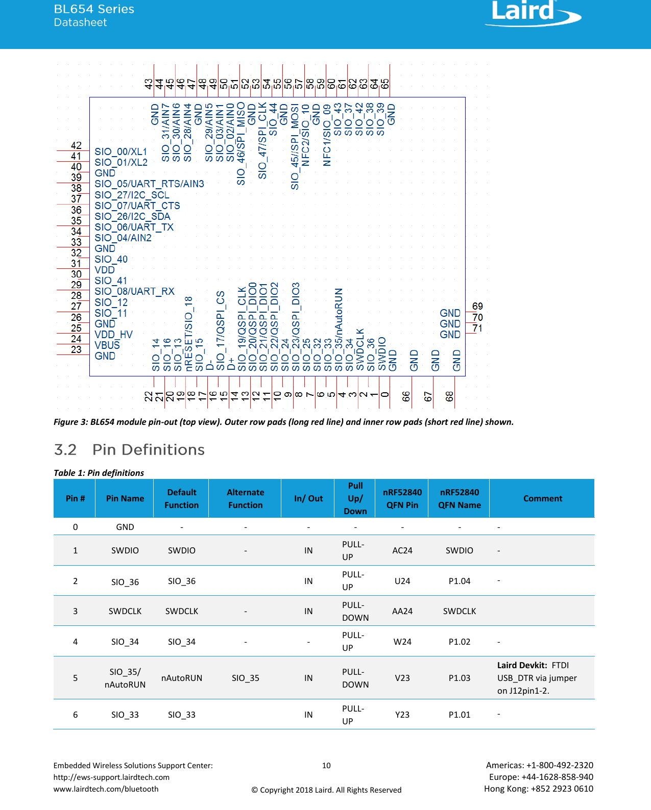
Laird Connectivity BL654 Bluetooth 5.0 BLE Data Module User Manual
Laird Technologies Bluetooth 5.0 BLE Data Module Users Manual
UserManual.wiki
>
Laird Connectivity
>
BL654 User Manual
>
Users Manual
Contents
1.
Users Manual
2.
User Manual
3.
Manual_CS-RegulatoryInfo-BL654
Users Manual
Navigation menu
Upload a User Manual
Namespaces
Wiki Guide
HTML
PDF
Info
Views
User Manual
Discussion / Help
Navigation
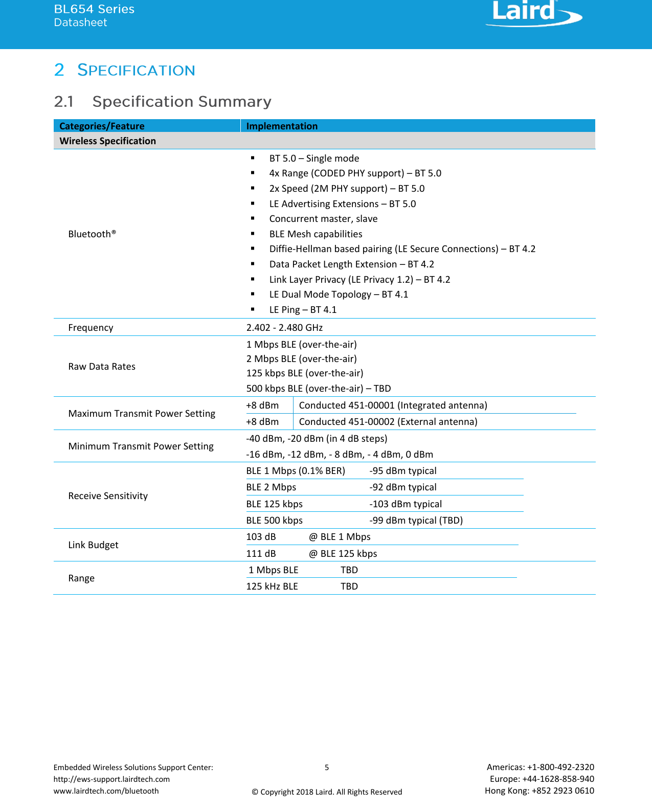
![Embedded Wireless Solutions Support Center: http://ews-support.lairdtech.com www.lairdtech.com/bluetooth 21 © Copyright 2018 Laird. All Rights Reserved Americas: +1-800-492-2320 Europe: +44-1628-858-940 Hong Kong: +852 2923 0610 Data taken at VDD of 3.0 V with internal (to chipset) LDO ON or with internal (to chipset) DCDC ON (see Power Consumption Note 1) and 25ºC. Table 9: Power consumption Parameter Min Typ Max Unit Active mode ‘peak’ current (Note 1) (Advertising or Connection) Tx only run peak current @ Txpwr = +8 dBm Tx only run peak current @ Txpwr = +4 dBm Tx only run peak current @ Txpwr = 0 dBm Tx only run peak current @ Txpwr = -4 dBm Tx only run peak current @ Txpwr = -8 dBm Tx only run peak current @ Txpwr = -12 dBm Tx only run peak current @ Txpwr = -16 dBm Tx only run peak current @ Txpwr = -20 dBm Tx only run peak current @ Txpwr = -40 dBm With DCDC [with LDO] 14.1 [30.4] 9.3 [18.9] 4.9 [10.2] 3.4 [7.3] 3.0 [6.4] 2.7 [5.7] 2.5 [5.3] 2.3 [5.0] 2.0 [4.0] mA mA mA mA mA mA mA mA mA Active Mode Rx only ‘peak’ current, BLE 1Mbps (Note 1) Rx only ‘peak’ current, BLE 2Mbps (Note 2) 4.8 [10.3] 5.4 [11.6] mA Ultra-Low Power Mode 1 (Note 2) Standby Doze, 64k RAM retention TBD uA Ultra-Low Power Mode 2 (Note 3) Deep Sleep (no RAM retention) TBD nA Active Mode Average current (Note 4) Advertising Average Current draw Max, with advertising interval (min) 20 mS Min, with advertising interval (max) 10240 mS Connection Average Current draw Max, with connection interval (min) 7.5 mS Min, with connection interval (max) 4000 mS ~TBD ~TBD ~TBD ~TBD uA uA uA uA Power Consumption Notes: Note 1 This is for Peak Radio Current only, but there is additional current due to the MCU. The internal DCDC convertor or LDO is decided by the underlying BLE stack. Note 2 BL654 modules Standby Doze is TBD uA typical. When using smartBASIC firmware, Standby Doze is entered automatically (when a waitevent statement is encountered within a smartBASIC application script). In Standby Doze, all peripherals that are enabled stay on and may re-awaken the chip. Depending on active peripherals, current consumption ranges from TBD μA to TBD uA (when UART is ON). See individual peripherals current consumption data in the Peripheral Block Current Consumption section. smartBASIC firmware has added new functionality to detect GPIO change with no current consumption cost, it is possible to close the UART and get to the TBD uA current consumption regime and still be able to](https://usermanual.wiki/Laird-Connectivity/BL654.Users-Manual/User-Guide-3905952-Page-21.png)