Laird Connectivity BL654 Bluetooth 5.0 BLE Data Module User Manual
Laird Technologies Bluetooth 5.0 BLE Data Module Users Manual
Contents
- 1. Users Manual
- 2. User Manual
- 3. Manual_CS-RegulatoryInfo-BL654
Users Manual
Version 0.5
This is a PRELIMINARY version of the BL654 datasheet.
Information contained in this document is subject to change.
Embedded Wireless Solutions Support Center:
http://ews-support.lairdtech.com
www.lairdtech.com/bluetooth
2
© Copyright 2018 Laird. All Rights Reserved
Americas: +1-800-492-2320
Europe: +44-1628-858-940
Hong Kong: +852 2923 0610
Version
Date
Notes
Contributor(s)
Approver
0.1
09 Feb 2018
Initial Release
Raj Khatri
Jonathan Kaye
0.2
21 Feb 2018
Updated antenna information
Connie Lin
Jonathan Kaye
0.3
12 Mar 2018
Updated mechanical drawing (rear)
Updated template to new style
Raj Khatri/Sean Querry
Jonathan Kaye
0.4
02 Apr 2018
Fixed part # error (455-0002 changed to
455-00002)
Karla Moreno
Jonathan Kaye
0.5
12 Apr 2018
Updated Power Supply block diagram
(figure 4)
Raj Khatri
Jonathan Kaye
0.6
08 May 2018
Updated Regulatory section
Connie Lin
Jonathan Kaye

Embedded Wireless Solutions Support Center:
http://ews-support.lairdtech.com
www.lairdtech.com/bluetooth
3
© Copyright 2018 Laird. All Rights Reserved
Americas: +1-800-492-2320
Europe: +44-1628-858-940
Hong Kong: +852 2923 0610
1 Overview and Key Features ................................................................................................................................................... 4
2 Specification .......................................................................................................................................................................... 5
3 Hardware Specifications ........................................................................................................................................................ 8
3.1 Block Diagram and Pin-out ........................................................................................................................................... 9
3.2 Pin Definitions ............................................................................................................................................................ 10
3.3 Electrical Specifications .............................................................................................................................................. 16
3.4 Programmability ......................................................................................................................................................... 20
4 Power Consumption ............................................................................................................................................................ 20
5 Functional Description ......................................................................................................................................................... 24
5.1 Power Management ................................................................................................................................................... 24
5.2 BL654 Power Supply Options ..................................................................................................................................... 24
5.3 Clocks and Timers ....................................................................................................................................................... 27
5.4 Radio Frequency (RF) ................................................................................................................................................. 27
5.5 NFC ............................................................................................................................................................................. 27
5.6 UART Interface ........................................................................................................................................................... 29
5.7 USB interface .............................................................................................................................................................. 30
5.8 SPI Bus ........................................................................................................................................................................ 30
5.9 I2C Interface ............................................................................................................................................................... 31
5.10 General Purpose I/O, ADC, PWM and FREQ ............................................................................................................... 31
5.11 nRESET pin .................................................................................................................................................................. 32
5.12 Two-wire Interface JTAG ............................................................................................................................................ 32
5.13 BL654 Wakeup ........................................................................................................................................................... 33
5.14 Low Power Modes ...................................................................................................................................................... 33
5.15 Temperature Sensor................................................................................................................................................... 34
5.16 Security/Privacy ......................................................................................................................................................... 34
5.16.1 Random Number Generator................................................................................................................................. 34
5.16.2 AES Encryption/Decryption .................................................................................................................................. 34
5.16.3 ARM Cryptocell ..................................................................................................................................................... 34
5.16.4 Readback Protection ............................................................................................................................................ 34
5.16.5 Elliptic Curve Cryptography .................................................................................................................................. 34
5.17 Optional External 32.768 kHz crystal ......................................................................................................................... 34
5.18 451-00001 On-board PCB Antenna Characteristics ................................................................................................... 36
6 Hardware Integration Suggestions ...................................................................................................................................... 36
6.1 Circuit ......................................................................................................................................................................... 36
6.2 PCB Layout on Host PCB - General ............................................................................................................................. 38
6.3 PCB Layout on Host PCB for the 451-00001 ............................................................................................................... 38
6.4 External Antenna Integration with the 451-00002 .................................................................................................... 40
7 Mechanical Details .............................................................................................................................................................. 40
8 Application Note for Surface Mount Modules .................................................................................................................... 42
8.1 Introduction ............................................................................................................................................................... 43
8.2 Shipping ...................................................................................................................................................................... 43
8.3 Reflow Parameters ..................................................................................................................................................... 46
9 FCC and IC Regulatory Statements ...................................................................................................................................... 48
10 Japan (MIC) Regulatory ....................................................................................................................................................... 52
11 CE Regulatory ...................................................................................................................................................................... 53
12 Ordering Information .......................................................................................................................................................... 54
13 Bluetooth SIG Qualification ................................................................................................................................................. 54
14 Additional Assistance .......................................................................................................................................................... 56
Embedded Wireless Solutions Support Center:
http://ews-support.lairdtech.com
www.lairdtech.com/bluetooth
4
© Copyright 2018 Laird. All Rights Reserved
Americas: +1-800-492-2320
Europe: +44-1628-858-940
Hong Kong: +852 2923 0610
Every BL654 Series module is designed to simplify OEMs enablement of Bluetooth Low Energy (BLE) v5.0 and Thread
(802.15.4) to small, portable, power-conscious devices. The BL654 provides engineers with considerable design flexibility in
both hardware and software programming capabilities. Based on the world-leading Nordic Semiconductor nRF52840 chipset,
the BL654 modules provide ultra-low power consumption with outstanding wireless range via +8 dBm of transmit power and
the Long Range (CODED PHY) Bluetooth 5 feature. The BL654 is programmable via Laird’s smartBASIC language or Nordic’s
software development kit (SDK).
smartBASIC is an event-driven programming language that is highly optimized for memory-constrained systems such as
embedded modules. It was designed to make BLE development quicker and simpler, vastly cutting down time to market.
The Nordic SDK, on the other hand, offers developers source code (in C) and precompiled libraries containing BLE and ANT+
device profiles, wireless communication, as well as application examples.
Note: BL654 hardware provides all functionality of the nRF52840 chipset used in the module design. This is a hardware
datasheet only – it does not cover the software aspects of the BL654.
For customers using smartBASIC, refer to the smartBASIC extensions guide (available from the BL654 product page
of the Laird website.
For customers using the Nordic SDK, refer to www.nordicsemi.com.
▪ Bluetooth v5.0 – Single mode
▪ NFC
▪ 802.15.4 (Thread) radio support
▪ External or internal antennas
▪ Multiple programming options
–
–
▪ Compact footprint
▪ Programmable Tx power +8 dBm to -20 dBm, -40dBm
▪ Rx sensitivity – -95 dBm
▪ Ultra-low power consumption
▪ Tx – 4.9 mA peak (at 0 dBm, DCDC on)
(See Note 1 in the Power Consumption section)
▪ Rx: 4.8 mA peak (DCDC on)
(See Note 1 in the Power Consumption section)
▪ Standby Doze – TBD uA typical
▪ Deep Sleep – TBD uA – (See Note 4 in the Power
Consumption section)
▪ UART, GPIO, ADC, PWM, FREQ output, timers, I2C,
SPI, I2S, PDM, and USB interfaces
▪ Fast time-to-market
▪ FCC, CE, IC, RCM and Japan certified
▪ Full Bluetooth Declaration ID
▪ Other regulatory certifications on request (all
certifications pending)
▪ No external components required
▪ Industrial temperature range (-40° C to +85° C)
▪ Medical devices
▪ IoT Sensors
▪ Appcessories
▪ Fitness sensors
▪ Location awareness
▪ Home automation
Note: Figures on this page are gathered from the nRF52840 datasheet provided by Nordic.
Embedded Wireless Solutions Support Center:
http://ews-support.lairdtech.com
www.lairdtech.com/bluetooth
5
© Copyright 2018 Laird. All Rights Reserved
Americas: +1-800-492-2320
Europe: +44-1628-858-940
Hong Kong: +852 2923 0610
Categories/Feature
Implementation
Wireless Specification
Bluetooth®
▪ BT 5.0 – Single mode
▪ 4x Range (CODED PHY support) – BT 5.0
▪ 2x Speed (2M PHY support) – BT 5.0
▪ LE Advertising Extensions – BT 5.0
▪ Concurrent master, slave
▪ BLE Mesh capabilities
▪ Diffie-Hellman based pairing (LE Secure Connections) – BT 4.2
▪ Data Packet Length Extension – BT 4.2
▪ Link Layer Privacy (LE Privacy 1.2) – BT 4.2
▪ LE Dual Mode Topology – BT 4.1
▪ LE Ping – BT 4.1
Frequency
2.402 - 2.480 GHz
Raw Data Rates
1 Mbps BLE (over-the-air)
2 Mbps BLE (over-the-air)
125 kbps BLE (over-the-air)
500 kbps BLE (over-the-air) – TBD
Maximum Transmit Power Setting
+8 dBm
Conducted 451-00001 (Integrated antenna)
+8 dBm
Conducted 451-00002 (External antenna)
Minimum Transmit Power Setting
-40 dBm, -20 dBm (in 4 dB steps)
-16 dBm, -12 dBm, - 8 dBm, - 4 dBm, 0 dBm
Receive Sensitivity
BLE 1 Mbps (0.1% BER)
-95 dBm typical
BLE 2 Mbps
-92 dBm typical
BLE 125 kbps
-103 dBm typical
BLE 500 kbps
-99 dBm typical (TBD)
Link Budget
103 dB
@ BLE 1 Mbps
111 dB
@ BLE 125 kbps
Range
1 Mbps BLE
TBD
125 kHz BLE
TBD
Embedded Wireless Solutions Support Center:
http://ews-support.lairdtech.com
www.lairdtech.com/bluetooth
6
© Copyright 2018 Laird. All Rights Reserved
Americas: +1-800-492-2320
Europe: +44-1628-858-940
Hong Kong: +852 2923 0610
Categories/Feature
Implementation
NFC
NFC-A Listen mode compliant
Based on NFC forum specification
▪ 13.56 MHz
▪ Date rate 106 kbps
▪ NFC Type2 and Type 4 emulation
Modes of Operation:
▪ Disable
▪ Sense
▪ Activated
Use Cases:
▪ Touch-to-Pair with NFC
▪ NFC enabled Out-of-Band Pairing
System Wake-On-Field function
Proximity Detection
Host Interfaces and Peripherals
Total
48 x multifunction I/O lines
UART
2 UARTs
Tx, Rx, CTS, RTS
DCD, RI, DTR, DSR (See Note 1)
Default 115200, n, 8, 1
From 1,200 bps to 1 Mbps
USB
USB2.0 FS (Full Speed, 12Mbps).
CDC driver / Virtual UART (baud rate TBD)
Other USB drivers available via Nordic SDK
GPIO
Up to 48, with configurable:
I/O direction,
O/P drive strength (standard 0.5 mA or high 3mA/5 mA),
Pull-up /pull-down
Input buffer disconnect
ADC
Eight 8/10/12-bit channels
0.6 V internal reference
Configurable 4, 2, 1, 1/2, 1/3, 1/4, 1/5 1/6(default) pre-scaling
Configurable acquisition time 3uS, 5uS, 10uS(default), 15uS, 20uS, 40uS.
One-shot mode
PWM Output
PWM outputs on 16 GPIO output pins.
▪ PWM output duty cycle: 0%-100%
▪ PWM output frequency: Up to 500kHz
(See Note 7)
FREQ Output
FREQ outputs on 16 GPIO output pins.
▪ FREQ output frequency: 0 MHz-4MHz (50% duty cycle)
I2C
Two I2C interface (up to 400 kbps) – See Note 2
SPI
Four SPI Master Slave interface (up to 4 Mbps)
QSPI
One 32-MHz QSPI interface. Gives XIP (Execution in Place) capability.
External serial flash IC must be fitted as per Nordic specifications.
Embedded Wireless Solutions Support Center:
http://ews-support.lairdtech.com
www.lairdtech.com/bluetooth
7
© Copyright 2018 Laird. All Rights Reserved
Americas: +1-800-492-2320
Europe: +44-1628-858-940
Hong Kong: +852 2923 0610
Categories/Feature
Implementation
Temperature Sensor
One temperature sensor.
Temperature range equal to the operating temperature range.
Resolution 0.25 degrees.
RSSI Detector
One RF received signal strength indicator
Two dB accuracy (valid over -90 to -20 dBm)
One dB resolution
I2S
One inter-IC sound interface
PDM
One pulse density modulation interface
Optional (External to the BL654 module)
External 32.768 kHz crystal
For customer use, connect +/-20ppm accuracy crystal for more accurate
protocol timing.
Profiles
Services supported
▪ Central Mode
▪ Peripheral Mode
▪ Mesh (with custom models)
▪ Custom and adopted profiles
Programmability
smartBASIC
FW upgrade via JTAG or UART
Application download via UART or Via Over-the-Air (if SIO_02 pin is pulled high
externally)
Nordic SDK
Via JTAG
Operating Modes
smartBASIC
Self-contained Run mode
Selected by nAutoRun pin status: LOW (0V).
Then runs $autorun$ (smartBASIC application script) if it exists.
Interactive/Development mode
HIGH (VDD).
Then runs via at+run (and file name of smartBASIC application script).
Nordic SDK
As per Nordic SDK
Supply Voltage
Supply (VDD or VDD_HV) options
▪ Normal voltage mode VDD 1.7- 3.6 V – Internal DCDC converter or LDO
(See Note 3)
OR
▪ High voltage mode VDD_HV 2.5V-5.5V Internal DCDC converter or LDO
(See Note 5)
Power Consumption
Active Modes Peak Current (for
maximum Tx power +8 dBm)
– Radio only
14.1 mA peak Tx (with DCDC)
Active Modes Peak Current (for Tx
power -40 dBm) – Radio only
4.0 mA peak Tx (with DCDC)
Active Modes Average Current
Depends on many factors, see Power Consumption
Embedded Wireless Solutions Support Center:
http://ews-support.lairdtech.com
www.lairdtech.com/bluetooth
8
© Copyright 2018 Laird. All Rights Reserved
Americas: +1-800-492-2320
Europe: +44-1628-858-940
Hong Kong: +852 2923 0610
Categories/Feature
Implementation
Ultra-low Power Modes
Standby Doze
TBD uA typical (Note 4)
Deep Sleep
TBD nA (Note 4)
Antenna Options
Internal
Printed PCB monopole antenna – on-board
451-00001 variant
External
▪ Dipole antenna (with IPEX connector)
▪ Dipole PCB antenna (with IPEX connector)
▪ Connection via IPEX MH4 – 451-00002 variant
See the Antenna Information sections for FCC and IC, MIC, RCM and CE.
Physical
Dimensions
15.0 mm x 10 mm x 2.2 mm
Pad Pitch – 0.8 mm
Pad Type – Two rows of pads.
Weight
<1 gram
Environmental
Operating
-40 ˚C to +85 ˚C
Storage
-40 ˚C to +85 ˚C
Miscellaneous
Lead Free
Lead-free and RoHS compliant
Warranty
One-Year Warranty
Development Tools
Development Kit
Development kit per module SKU (455-00001 and 455-00002) and free
software tools
Approvals
Bluetooth®
Full Bluetooth SIG Declaration ID (all pending)
FCC / IC / CE / MIC / RCM
All BL654 Series (all pending)
Module Specification Notes:
Note 1
DSR, DTR, RI, and DCD can be implemented in the smartBASIC application or through the Nordic SDK.
Note 2
With I2C interface selected, pull-up resistors on I2C SDA and I2C SCL must be connected externally as per I2C
standard.
Note 3
Use of the internal DCDC convertor or LDO is decided by the underlying BLE stack.
Note 4
These figures are measured on the BL654 modules
▪ Deep Sleep current for BL654 modules TBD uA (typical)
▪ Standby Doze current for BL654 modules – TBD uA (typical)
Embedded Wireless Solutions Support Center:
http://ews-support.lairdtech.com
www.lairdtech.com/bluetooth
9
© Copyright 2018 Laird. All Rights Reserved
Americas: +1-800-492-2320
Europe: +44-1628-858-940
Hong Kong: +852 2923 0610
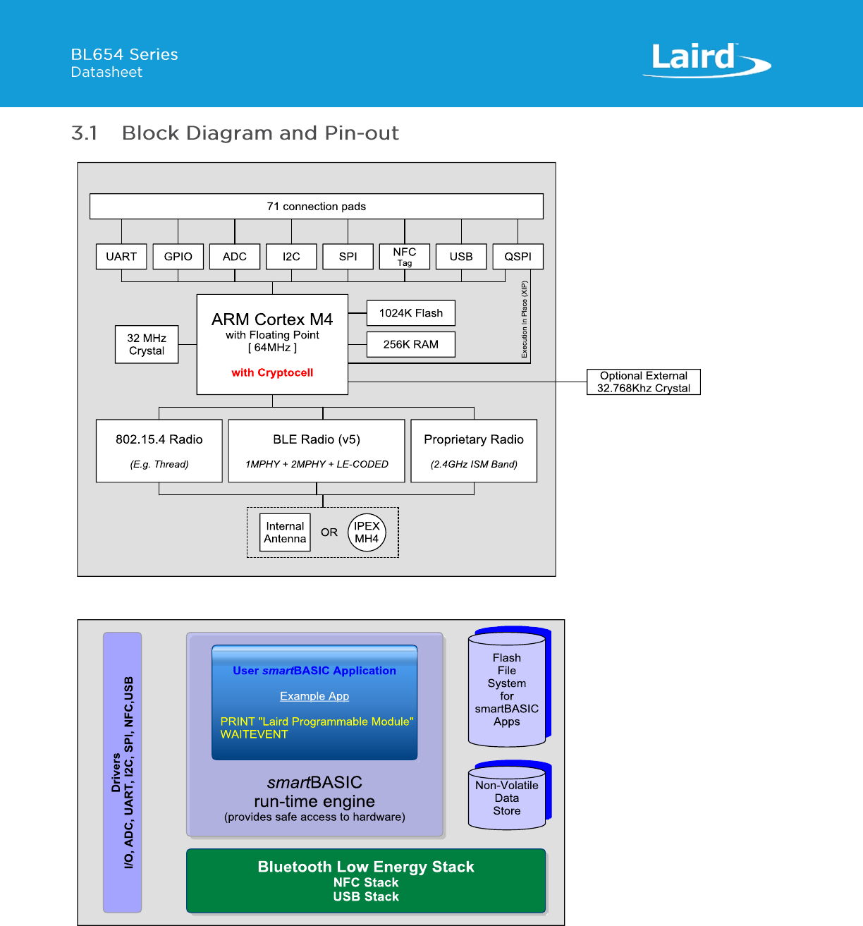
Figure 1: BL654 Block diagram
Figure 2: Functional HW and SW block diagram for BL654 series BLE module
Embedded Wireless Solutions Support Center:
http://ews-support.lairdtech.com
www.lairdtech.com/bluetooth
10
© Copyright 2018 Laird. All Rights Reserved
Americas: +1-800-492-2320
Europe: +44-1628-858-940
Hong Kong: +852 2923 0610
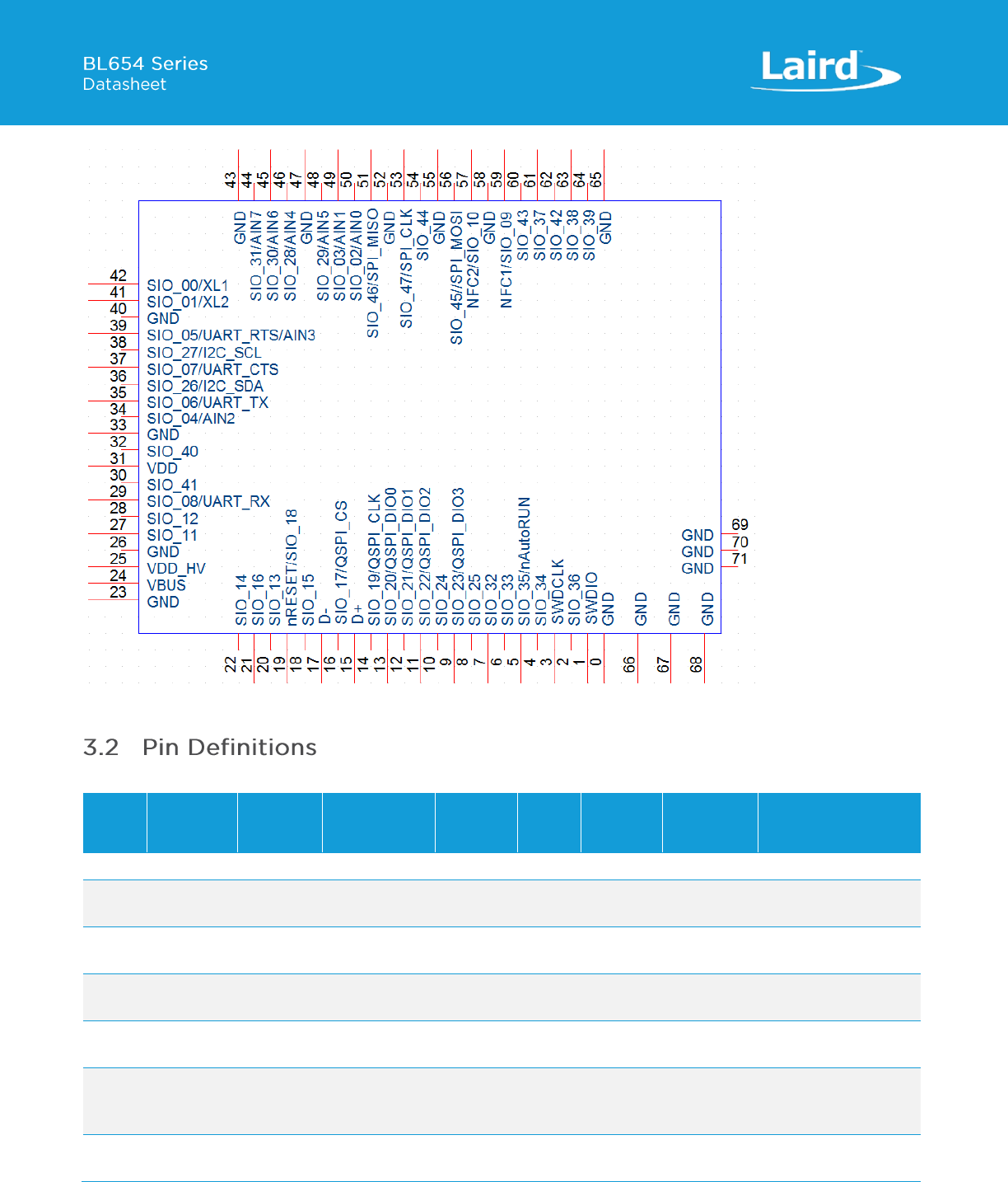
Figure 3: BL654 module pin-out (top view). Outer row pads (long red line) and inner row pads (short red line) shown.
Table 1: Pin definitions
Pin #
Pin Name
Default
Function
Alternate
Function
In/ Out
Pull
Up/
Down
nRF52840
QFN Pin
nRF52840
QFN Name
Comment
0
GND
-
-
-
-
-
-
-
1
SWDIO
SWDIO
-
IN
PULL-
UP
AC24
SWDIO
-
2
SIO_36
SIO_36
IN
PULL-
UP
U24
P1.04
-
3
SWDCLK
SWDCLK
-
IN
PULL-
DOWN
AA24
SWDCLK
4
SIO_34
SIO_34
-
-
PULL-
UP
W24
P1.02
-
5
SIO_35/
nAutoRUN
nAutoRUN
SIO_35
IN
PULL-
DOWN
V23
P1.03
Laird Devkit: FTDI
USB_DTR via jumper
on J12pin1-2.
6
SIO_33
SIO_33
IN
PULL-
UP
Y23
P1.01
-
Embedded Wireless Solutions Support Center:
http://ews-support.lairdtech.com
www.lairdtech.com/bluetooth
11
© Copyright 2018 Laird. All Rights Reserved
Americas: +1-800-492-2320
Europe: +44-1628-858-940
Hong Kong: +852 2923 0610
Pin #
Pin Name
Default
Function
Alternate
Function
In/ Out
Pull
Up/
Down
nRF52840
QFN Pin
nRF52840
QFN Name
Comment
7
SIO_32
SIO_32
-
IN
PULL-
UP
AD22
P1.00
-
8
SIO_25
SIO_25
-
IN
PULL-
UP
AC21
PO.25
Laird Devkit:
BUTTON1
9
SIO_23
SIO_23
QSPI_DIO3
IN
PULL-
UP
AC19
PO.23
-
10
SIO_24
SIO_24
IN
PULL-
UP
AD20
PO.24
Laird Devkit:
BUTTON3
11
SIO_22
SIO_22
QSPI_DIO2
IN
PULL-
UP
AD18
PO.22
-
12
SIO_21
SIO_21
QSPI_DIO1
IN
PULL-
UP
AC17
PO.21
-
13
SIO_20
SIO_20
QSPI_DIO0
IN
PULL-
UP
AD16
PO.20
-
14
SIO_19
SIO_19
QSPI_CLK
IN
PULL-
UP
AC15
PO.19
-
15
D+
D+
-
IN
AD6
D+
-
16
SIO_17
SIO_17
QSPI_CS
IN
PULL-
UP
AD12
PO.17
-
17
D-
D-
-
IN
AD4
D-
-
18
SIO_15
SIO_15
-
IN
PULL-
UP
AD10
PO.15
Laird Devkit: LED3
19
nRESET
nRESET
SIO_18
IN
PULL-
UP
AC13
PO.18
System Reset (Active
Low)
20
SIO_13
SIO_13
-
IN
PULL-
UP
AD8
PO.13
Laird Devkit: LED1
21
SIO_16
SIO_16
-
IN
PULL-
UP
AC11
PO.16
Laird Devkit: LED4
22
SIO_14
SIO_14
-
IN
PULL-
UP
AC9
PO.14
Laird Devkit: LED2
23
GND
-
-
-
-
-
-
-
24
VBUS
4.35V – 5.5V
25
VDD_HV
-
-
-
-
-
-
2.5V to 5.5V
26
GND
-
-
-
-
-
-
-
27
SIO_11
SIO_11
-
IN
PULL-
UP
T2
PO.11
Laird Devkit:
BUTTON1
28
SIO_12
SIO_12
-
IN
PULL-
UP
U1
PO.12
-
Embedded Wireless Solutions Support Center:
http://ews-support.lairdtech.com
www.lairdtech.com/bluetooth
12
© Copyright 2018 Laird. All Rights Reserved
Americas: +1-800-492-2320
Europe: +44-1628-858-940
Hong Kong: +852 2923 0610
Pin #
Pin Name
Default
Function
Alternate
Function
In/ Out
Pull
Up/
Down
nRF52840
QFN Pin
nRF52840
QFN Name
Comment
29
SIO_08/
UART_RX
SIO_08
UART_RX
IN
PULL-
UP
N1
PO.08
UARTCLOSE() selects
DIO functionality.
UARTOPEN() selects
UART COMMS
behaviour
30
SIO_41
SIO_41
-
IN
PULL-
UP
R1
P1.09
-
31
VDD
-
-
-
-
1.7V to 3.6V
32
SIO_40
SIO_40
-
IN
PULL-
UP
P2
P1.08
-
33
GND
-
-
-
-
-
-
-
34
SIO_04/
AIN2
SIO_04
AIN2
IN
PULL-
UP
J1
PO.04/AIN2
-
35
SIO_06/
UART_TX
SIO_06
UART_TX
OUT
Set
High
in FW
L1
PO.06
UARTCLOSE() selects
DIO functionality.
UARTOPEN() selects
UART COMMS
behaviour
36
SIO_26/
I2C_SDA
SIO_26
I2C_SDA
IN
PULL-
UP
G1
PO.26
Laird Devkit: I2C RTC
chip. I2C data line.
37
SIO_07/
UART_CTS
SIO_07
UART_CTS
IN
PULL-
DOWN
M2
PO.07
UARTCLOSE() selects
DIO functionality.
UARTOPEN() selects
UART COMMS
behaviour
38
SIO_27/
I2C_SCL
SIO_27
I2C_SCL
IN
PULL-
UP
H2
PO.27
Laird Devkit: I2C RTC
chip. I2C clock line.
39
SIO_05/
UART_RTS/
AIN3
SIO_05
UART_RTS/
AIN3
OUT
Set
Low in
FW
K2
PO.05/AIN3
UARTCLOSE() selects
DIO functionality.
UARTOPEN() selects
UART COMMS
behaviour
40
GND
-
-
-
-
-
-
-
41
SIO_01/
XL2
SIO_01
XL2
IN
PULL-
UP
F2
PO.01/XL2
Laird Devkit: Optional
32.768kHz crystal pad
XL2 and associated
load capacitor.
42
SIO_00/
XL1
SIO_00
XL1
IN
PULL-
UP
D2
PO.00/XL1
Laird Devkit: Optional
32.768kHz crystal pad
XL1 and associated
load capacitor.
43
GND
-
-
-
-
-
-
-
44
SIO_31/
AIN7
SIO_31
AIN7
IN
PULL-
UP
A8
PO.31/AIN7
-
Embedded Wireless Solutions Support Center:
http://ews-support.lairdtech.com
www.lairdtech.com/bluetooth
13
© Copyright 2018 Laird. All Rights Reserved
Americas: +1-800-492-2320
Europe: +44-1628-858-940
Hong Kong: +852 2923 0610
Pin #
Pin Name
Default
Function
Alternate
Function
In/ Out
Pull
Up/
Down
nRF52840
QFN Pin
nRF52840
QFN Name
Comment
45
SIO_30/
AIN6
SIO_30
AIN6
IN
PULL-
UP
B9
PO.30/AIN6
-
46
SIO_28/
AIN4
SIO_28
AIN4
IN
PULL-
UP
B11
PO.28/AIN4
-
47
GND
-
-
-
-
-
-
-
48
SIO_29/
AIN5
SIO_29
AIN5
IN
PULL-
UP
A1-
PO.29/AIN5
-
49
SIO_03/
AIN1
SIO_03
AIN1
IN
PULL-
UP
B13
PO.03/AIN1
Laird Devkit: Temp
Sens Analog
50
SIO_02/
AIN0
SIO_02
AIN0
IN
PULL-
DOWN
A12
PO.02/AIN0
Internal pull-down. Pull
High externally to
enter VSP (Virtual
Serial Port) Service.
51
SIO_46/
SPI_MISO
SIO_46
SPI_MISO
IN
PULL-
UP
B15
P1.14
Laird Devkit: SPI
EEPROM.
SPI_Eeprom_MISO,
Input.
SPIOPEN() in
smartBASIC selects SPI
function; MOSI and
CLK are outputs when
in SPI master mode.
52
GND
-
-
-
-
-
-
-
53
SIO_47/
SPI_CLK
SIO_47
SPI_CLK
IN
PULL-
UP
A14
P1.15
Laird Devkit: SPI
EEPROM.
SPI_Eeprom_CLK,
Output:
SPIOPEN() in
smartBASIC selects SPI
function, MOSI and CLK
are outputs when in
SPI master mode.
54
SIO_44
SIO_44
-
IN
PULL-
UP
B17
P1.12
Laird Devkit: SPI
EEPROM.
SPI_Eeprom_CS, Input
55
GND
-
-
-
-
-
-
-
Embedded Wireless Solutions Support Center:
http://ews-support.lairdtech.com
www.lairdtech.com/bluetooth
14
© Copyright 2018 Laird. All Rights Reserved
Americas: +1-800-492-2320
Europe: +44-1628-858-940
Hong Kong: +852 2923 0610
Pin #
Pin Name
Default
Function
Alternate
Function
In/ Out
Pull
Up/
Down
nRF52840
QFN Pin
nRF52840
QFN Name
Comment
56
SIO_45/
SPI_MOSI
SIO_45
SPI_MOSI
IN
PULL-
UP
A16
P1.13
Laird Devkit: SPI
EEPROM.
SPI_Eeprom_MOSI,
Output
SPIOPEN() in
smartBASIC selects SPI
function, MOSI and CLK
are outputs in SPI
master.
57
NFC2/
SIO_10
NFC2
SIO_10
IN
-
J24
PO.10/NFC2
-
58
GND
-
-
-
-
-
-
-
59
NFC1/
SIO_09
NFC1
SIO_09
IN
-
L24
PO.09/NFC1
-
60
SIO_43
SIO_43
-
IN
PULL-
UP
B19
P1.11
-
61
SIO_37
SIO_37
-
IN
PULL-
UP
T23
P1.05
-
62
SIO_42
SIO_42
-
IN
PULL-
UP
A20
P1.10
-
63
SIO_38
N/C
-
IN
PULL-
UP
R24
P1.06
Reserved for future
use. Do not connect.
64
SIO_39
SIO_39
-
IN
PULL-
UP
P23
P1.07
-
65
GND
-
-
-
-
-
-
-
66
GND
-
-
-
-
-
-
-
67
GND
-
-
-
-
-
-
-
68
GND
-
-
-
-
-
-
-
69
GND
-
-
-
-
-
-
-
70
GND
-
-
-
-
-
-
-
71
GND
-
-
-
-
-
-
-
Pin Definition Notes:
Note 1
SIO = Signal Input or Output. Secondary function is selectable in smartBASIC application or via Nordic SDK. I/O
voltage level tracks VDD. AIN = Analog Input.
Note 2
At reset, all SIO lines are configured as the defaults shown above.
SIO lines can be configured through the smartBASIC application script to be either inputs or outputs with pull-
ups or pull-downs. When an alternative SIO function is selected (such as I2C or SPI), the firmware does not
allow the setup of internal pull-up/pull-down. Therefore, when I2C interface is selected, pull-up resistors on I2C

Embedded Wireless Solutions Support Center:
http://ews-support.lairdtech.com
www.lairdtech.com/bluetooth
15
© Copyright 2018 Laird. All Rights Reserved
Americas: +1-800-492-2320
Europe: +44-1628-858-940
Hong Kong: +852 2923 0610
Pin Definition Notes:
SDA and I2C SCL must be connected externally as per I2C standard.
Note 3
JTAG (two-wire SWD interface), pin 1 (SWDIO) and pin 3 (SWDCLK).
JTAG is required because Nordic SDK applications can only be loaded using JTAG (smartBASIC firmware can be
loaded using the JTAG as well as UART). We recommend that you use JTAG (2-wire interface) to handle future
BL654 module smartBASIC firmware upgrades. You MUST wire out the JTAG (2-wire interface) on your host
design (see Figure 7, where four lines (SWDIO, SWDCLK, GND and VDD) should be wired out. smartBASIC
firmware upgrades can still be performed over the BL654 UART interface, but this is slower (60 seconds using
UART vs. 10 seconds when using JTAG) than using the BL654 JTAG (2-wire interface).
Upgrading smartBASIC firmware or loading the smartBASIC applications is done using the UART interface.
Note 4
Pull the nRESET pin (pin 19) low for minimum 100 milliseconds to reset the BL654.
Note 5
The SIO_02 pin (pin 50) must be pulled high externally to enable VSP (Virtual Serial Port) which would allow
OTA (over-the-air) smartBASIC application download. Refer to the latest firmware release documentation for
details.
Note 6
Note 7
Ensure that SIO_02 (pin 50) and AutoRUN (pin 5) are not both high (externally), in that state, the UART is
bridged to Virtual Serial Port service; the BL654 module does not respond to AT commands and cannot load
smartBASIC application scripts.
Pin 5 (nAutoRUN) is an input, with active low logic. In the development kit it is connected so that the state is
driven by the host’s DTR output line. The nAutoRUN pin must be externally held high or low to select between
the following two BL654 operating modes:
▪ Self-contained Run mode (nAutoRUN pin held at 0V –this is the default (internal pull-down enabled))
▪ Interactive/Development mode (nAutoRUN pin held at VDD)
The smartBASIC firmware checks for the status of nAutoRUN during power-up or reset. If it is low and if there is
a smartBASIC application script named $autorun$, then the smartBASIC firmware executes the application
script automatically; hence the name Self-contained Run Mode.
Note 8
The smartBASIC firmware has SIO pins as Digital (Default Function) INPUT pins, which are set PULL-UP by
default. This avoids floating inputs (which can cause current consumption to drive with time in low power
modes (such as Standby Doze). You can disable the PULL-UP through your smartBASIC application.
All of the SIO pins (with a default function of DIO) are inputs (apart from SIO_05 and SIO_06, which are
outputs):
▪ SIO_06 (alternative function UART_TX) is an output, set High (in the firmware).
▪ SIO_05 (alternative function UART_RTS) is an output, set Low (in the firmware).
▪ SIO_08 (alternative function UART_RX) is an input, set with internal pull-up (in the firmware).
▪ SIO_07 (alternative function UART_CTS) is an input, set with internal pull-down (in the firmware).
▪ SIO_02 is an input set with internal pull-down (in the firmware). It is used for OTA downloading of
smartBASIC applications. Refer to the latest firmware extension documentation for details.
▪ UART_RX, UART_TX, and UART_CTS are 3.3 V level logic (if VDD is 3.3 V; such as SIO pin I/O levels track
VDD). For example, when Rx and Tx are idle, they sit at 3.3 V (if VDD is 3.3 V). Conversely, handshaking
pins CTS and RTS at 0V are treated as assertions.
Note 9
Not required for BL654 module normal operation. The on-chip 32.768kHz RC oscillator provides the standard
Embedded Wireless Solutions Support Center:
http://ews-support.lairdtech.com
www.lairdtech.com/bluetooth
16
© Copyright 2018 Laird. All Rights Reserved
Americas: +1-800-492-2320
Europe: +44-1628-858-940
Hong Kong: +852 2923 0610
Pin Definition Notes:
Note 10
accuracy of ±250 ppm, with calibration required every 8seconds (default) to stay within ±250 ppm.
BL654 also allows as an option to connect an external higher accuracy (±20 ppm) 32.768 kHz crystal to the
BL654 pins SIO_01/XL2 (pin 41) and SIO_00/XL1 (pin 42). This provides higher accuracy protocol timing and
helps with radio power consumption in the system standby doze/deep sleep modes by reducing the time that
the Rx window must be open.
BL654 power supply options:
▪ Option 1 – Normal voltage power supply mode entered when the external supply voltage is connected to
both the VDD and VDD_HV pins (so that VDD equals VDD_HV). Connect external supply within range 1.7V
to 3.6V range to BL654 VDD and VDD_HV pins.
OR
▪ Option 2 – High voltage mode power supply mode (using BL654 VDD_HV pin) entered when the external
supply voltage in ONLY connected to the VDDH pin and the VDD pin is not connected to any external
voltage supply. Connect external supply within range 2.5V to 5.5V range to BL654 VDD_HV pin. BL654
VDD pin left unconnected.
For either option, if you use USB interface then the BL654 VBUS pin must be connected to external supply
within the range 4.35V to 5.5V. When using the BL654 VBUS pin, you MUST externally fit a 4.7uF to ground.
Absolute maximum ratings for supply voltage and voltages on digital and analogue pins of the module are listed below;
exceeding these values causes permanent damage.
Table 2: Maximum current ratings
Parameter
Min
Max
Unit
Voltage at VDD pin
-0.3
+3.9 (Note 1)
V
Voltage at VDD_HV pin
-0.3
+5.8
V
VBUS
-0.3
+5.8
V
Voltage at GND pin
0
V
Voltage at SIO pin (at VDD≤3.6V)
-0.3
VDD +0.3
V
Voltage at SIO pin (at VDD≥3.6V)
-0.3
3.9
V
NFC antenna pin current (NFC1/2)
-
80
mA
Radio RF input level
-
10
dBm
Environmental
Storage temperature
-40
+85
ºC
MSL (Moisture Sensitivity Level)
-
4
-
ESD (as per EN301-489)
Conductive
Air Coupling
4
8
KV
KV
Flash Memory (Endurance) (Note 2)
-
10000
Write/erase cycles
Flash Memory (Retention)
-
10 years at 40°C
-
Embedded Wireless Solutions Support Center:
http://ews-support.lairdtech.com
www.lairdtech.com/bluetooth
17
© Copyright 2018 Laird. All Rights Reserved
Americas: +1-800-492-2320
Europe: +44-1628-858-940
Hong Kong: +852 2923 0610
Maximum Ratings Notes:
Note 1
The absolute maximum rating for VDD_nRFin (max) is 3.9V for the BL654.
Note 2
Wear levelling is used in file system.
Table 3: Power supply operating parameters
Parameter
Min
Typ
Max
Unit
VDD (independent of DCDC)1 supply range
1.7
3.3
3.6
V
VDD_HV (independent of DCDC) supply range
2.5
3.7
5.5
V
VBUS USB supply range
4.35
5
5.5
V
VDD Maximum ripple or noise2
-
-
10
mV
VDD supply rise time (0V to 1.7V)3
Time in Power
-
-
60
mS
mS
mS
mS
VDD_HV supply rise time (0V to 3.7V) 3
100
mS
Operating Temperature Range
-40
-
+85
ºC
Recommended Operating Parameters Notes:
Note 1
4.7 uF internal to module on VDD. The internal DCDC convertor or LDO is decided by the underlying BLE stack.
Note 2
This is the maximum VDD or VDD_HV ripple or noise (at any frequency) that does not disturb the radio.
Note 3
The on-board power-on reset circuitry may not function properly for rise times longer than the specified
maximum.
Note 4
BL654 power supply options:
▪ Option 1 – Normal voltage power supply mode entered when the external supply voltage is connected to
both the VDD and VDD_HV pins (so that VDD equals VDD_HV). Connect external supply within range 1.7V
to 3.6V range to BL654 VDD and VDD_HV pins.
OR
▪ Option 2 – High voltage mode power supply mode (using BL654 VDD_HV pin) entered when the external
supply voltage in ONLY connected to the VDD_HV pin and the VDD pin is not connected to any external
voltage supply. Connect external supply within range 2.5V to 5.5V range to BL654 VDD_HV pin. BL654
VDD pin left unconnected.
For either option, if you use USB interface then the BL654 VBUS pin must be connected to external supply
within the range 4.35V to 5.5V. When using the BL654 VBUS pin, you MUST externally fit a 4.7uF to ground.
Embedded Wireless Solutions Support Center:
http://ews-support.lairdtech.com
www.lairdtech.com/bluetooth
18
© Copyright 2018 Laird. All Rights Reserved
Americas: +1-800-492-2320
Europe: +44-1628-858-940
Hong Kong: +852 2923 0610
Table 4: Signal levels for interface, SIO
Parameter
Min
Typ
Max
Unit
VIH Input high voltage
0.7 VDD
VDD
V
VIL Input low voltage
VSS
0.3 x VDD
V
VOH Output high voltage
(std. drive, 0.5mA) (Note 1)
(high-drive, 3mA) (Note 1)
(high-drive, 5mA) (Note 2)
VDD -0.4
VDD -0.4
VDD -0.4
VDD
VDD
VDD
V
V
VOL Output low voltage
(std. drive, 0.5mA) (Note 1)
(high-drive, 3mA) (Note 1)
(high-drive, 5mA) (Note 2)
VSS
VSS
VSS
VSS+0.4
VSS+0.4
VSS+0.4
V
V
VOL Current at VSS+0.4V, Output set low
(std. drive, 0.5mA) (Note 1)
(high-drive, 3mA) (Note 1)
(high-drive, 5mA) (Note 2)
1
3
6
2
-
10
4
-
15
mA
mA
mA
VOL Current at VDD -0.4, Output set low
(std. drive, 0.5mA) (Note 1)
(high-drive, 3mA) (Note 1)
(high-drive, 5mA) (Note 2)
1
3
6
2
-
9
4
-
14
mA
mA
mA
Pull up resistance
11
13
16
kΩ
Pull down resistance
11
13
16
kΩ
Pad capacitance
3
pF
Pad capacitance at NFC pads
4
pF
Signal Levels Notes:
Note 1
For VDD≥1.7V. The firmware supports high drive (3 mA, as well as standard drive).
Note 2
For VDD≥2.7V. The firmware supports high drive (5 mA (since VDD≥2.7V), as well as standard drive).
The GPIO (SIO) high reference voltage always equals the level on the VDD pin.
▪ Normal voltage mode – The GPIO high level equals the voltage supplied to the VDD pin
▪ High voltage mode – The GPIO high level equals the level specified (configurable TBD).
Embedded Wireless Solutions Support Center:
http://ews-support.lairdtech.com
www.lairdtech.com/bluetooth
19
© Copyright 2018 Laird. All Rights Reserved
Americas: +1-800-492-2320
Europe: +44-1628-858-940
Hong Kong: +852 2923 0610
Table 5: SIO pin alternative function AIN (ADC) specification
Parameter
Min
Typ
Max
Unit
Maximum sample rate
200
kHz
ADC Internal reference voltage
-1.5%
0.6 V
+1.5%
%
ADC pin input
internal selectable scaling
4, 2, 1, 1/2,
1/3, 1/4, 1/5
1/6
scaling
ADC input pin (AIN) voltage maximum without
damaging ADC w.r.t1
VCC Prescaling
0V-VDD 4, 2, 1, ½, 1/3, ¼, 1/5, 1/6
VDD+0.3
V
Configurable
Resolution
8-bit mode
10-bit mode
12-bit mode
bits
Configurable 2
Acquisition Time, source resistance ≤10kΩ
Acquisition Time, source resistance ≤40kΩ
Acquisition Time, source resistance ≤100kΩ
Acquisition Time, source resistance ≤200kΩ
Acquisition Time, source resistance ≤400kΩ
Acquisition Time, source resistance ≤800kΩ
3
5
10
15
20
40
uS
uS
uS
uS
uS
uS
Conversion Time3
<2
uS
ADC input impedance (during operation)3
Input Resistance
Sample and hold capacitance at maximum gain
>1
2.5
MOhm
pF
Recommended Operating Parameters Notes:
Note 1
Stay within internal 0.6 V reference voltage with given pre-scaling on AIN pin and do not violate ADC maximum
input voltage (for damage) for a given VCC, e.g. If VD is 3.6V, you can only expose AIN pin to VDD+0.3 V.
Default pre-scaling is 1/6 which configurable via smartBASIC.
Note 2
Firmware allows configurable resolution (8-bit, 10-bit or 12-bit mode) and acquisition time. The sampling
frequency is limited by the sum of sampling time and acquisition time. The maximum sampling time is 2us. For
acquisition time of 3us the total conversion time is therefore 5us, which makes maximum sampling frequency
of 1/5us = 200kHz. Similarly, if acquisition time of 40us chosen, then the conversion time is 42us and the
maximum sampling frequency is 1/42us = 23.8kHz
Note 3
ADC input impedance is estimated mean impedance of the ADC (AIN) pins.
Embedded Wireless Solutions Support Center:
http://ews-support.lairdtech.com
www.lairdtech.com/bluetooth
20
© Copyright 2018 Laird. All Rights Reserved
Americas: +1-800-492-2320
Europe: +44-1628-858-940
Hong Kong: +852 2923 0610
3.4.1 BL654 Default Firmware
The BL654 module comes loaded with smartBASIC firmware but does not come loaded with any smartBASIC application
script (as that is dependent on customer-end application or use). Laird provides many sample smartBASIC application scripts
via a sample application folder on GitHub – https://github.com/LairdCP/BL654-Applications
Therefore, it boots into AT command mode by default.
Refer to the smartBASIC extension manual for details of functionality connected to this:
▪ nAutoRUN pin (SIO_35), see Table 6 for default
▪ VSP pin (SIO_02), see Table 7 for default
▪ SIO_38 – Reserved for future use. Do not connect. See Table 8
Table 6: nAutoRUN pin
Signal Name
Pin #
I/O
Comments
nAutoRUN /(SIO_35)
5
I
Input with active low logic. Internal pull down (default).
Operating mode selected by nAutoRun pin status:
▪ Self-contained Run mode (nAutoRUN pin held at 0V).
If Low (0V), runs $autorun$ if it exists
▪ Interactive/Development mode (nAutoRUN pin held at VCC).
If High (VCC), runs via at+run (and file name of application)
In the development board nAutoRUN pin is connected so that the state is driven by the host’s DTR output line.
Table 7: VSP mode
Signal Name
Pin #
I/O
Comments
SIO_02
50
I
Internal pull down (default).
VSP mode selected by externally pulling-up SIO_02 pin:
High (VCC), then OTA smart BASIC application download is possible.
Table 8: SIO_38
Signal Name
Pin #
I/O
Comments
SIO_38
63
I
Internal pull up (default).
Reserved for future use. Do not connect.
Embedded Wireless Solutions Support Center:
http://ews-support.lairdtech.com
www.lairdtech.com/bluetooth
21
© Copyright 2018 Laird. All Rights Reserved
Americas: +1-800-492-2320
Europe: +44-1628-858-940
Hong Kong: +852 2923 0610
Data taken at VDD of 3.0 V with internal (to chipset) LDO ON or with internal (to chipset) DCDC ON (see Power Consumption
Note 1) and 25ºC.
Table 9: Power consumption
Parameter
Min
Typ
Max
Unit
Active mode ‘peak’ current (Note 1)
(Advertising or Connection)
Tx only run peak current @ Txpwr = +8 dBm
Tx only run peak current @ Txpwr = +4 dBm
Tx only run peak current @ Txpwr = 0 dBm
Tx only run peak current @ Txpwr = -4 dBm
Tx only run peak current @ Txpwr = -8 dBm
Tx only run peak current @ Txpwr = -12 dBm
Tx only run peak current @ Txpwr = -16 dBm
Tx only run peak current @ Txpwr = -20 dBm
Tx only run peak current @ Txpwr = -40 dBm
With DCDC [with LDO]
14.1 [30.4]
9.3 [18.9]
4.9 [10.2]
3.4 [7.3]
3.0 [6.4]
2.7 [5.7]
2.5 [5.3]
2.3 [5.0]
2.0 [4.0]
mA
mA
mA
mA
mA
mA
mA
mA
mA
Active Mode
Rx only ‘peak’ current, BLE 1Mbps (Note 1)
Rx only ‘peak’ current, BLE 2Mbps (Note 2)
4.8 [10.3]
5.4 [11.6]
mA
Ultra-Low Power Mode 1 (Note 2)
Standby Doze, 64k RAM retention
TBD
uA
Ultra-Low Power Mode 2 (Note 3)
Deep Sleep (no RAM retention)
TBD
nA
Active Mode Average current (Note 4)
Advertising Average Current draw
Max, with advertising interval (min) 20 mS
Min, with advertising interval (max) 10240 mS
Connection Average Current draw
Max, with connection interval (min) 7.5 mS
Min, with connection interval (max) 4000 mS
~TBD
~TBD
~TBD
~TBD
uA
uA
uA
uA
Power Consumption Notes:
Note 1
This is for Peak Radio Current only, but there is additional current due to the MCU. The internal DCDC
convertor or LDO is decided by the underlying BLE stack.
Note 2
BL654 modules Standby Doze is TBD uA typical. When using smartBASIC firmware, Standby Doze is entered
automatically (when a waitevent statement is encountered within a smartBASIC application script). In Standby
Doze, all peripherals
that are enabled stay on and may re-awaken the chip. Depending on active peripherals, current
consumption ranges from TBD μA to TBD uA (when UART is ON). See individual peripherals current
consumption data in the Peripheral Block Current Consumption section. smartBASIC
firmware has added new functionality to detect GPIO change with no current consumption cost, it is
possible to close the UART and get to the TBD uA current consumption regime and still be able to
Embedded Wireless Solutions Support Center:
http://ews-support.lairdtech.com
www.lairdtech.com/bluetooth
22
© Copyright 2018 Laird. All Rights Reserved
Americas: +1-800-492-2320
Europe: +44-1628-858-940
Hong Kong: +852 2923 0610
Power Consumption Notes:
detect for incoming data and be woken up so that the UART can be re-opened at expense of losing
that first character.
The BL654 Standby Doze current consists of the below nRF52840 blocks:
▪ nRF52 System ON IDLE current (no RAM retention) (0.7 uA) – This is the base current of the CPU
▪ LFRC (TBD uA) and RTC (TBDuA) running as well as 64k RAM retention (0.48 uA) – This adds to the total of
TBD uA typical.
Note 3
In Deep Sleep, everything is disabled and the only wake-up sources (including NFC to wakeup) are reset and
changes on SIO or NFC pins on which sense is enabled. The current consumption seen is ~TBD nA typical in
BL654 modules.
▪ Coming out from Deep Sleep to Standby Doze through the reset vector.
Note 4
Data taken with a transmit power of 8 dBm and all peripherals off (UART OFF after radio event), slave latency
of 0 (in a connection). Average current consumption depends on several factors (including Tx power, VCC,
accuracy of 32MHz and 32.768 kHz). With these factors fixed, the largest variable is the advertising or
connection interval set.
Advertising Interval range:
▪ 20 milliseconds to 10240 milliseconds in multiples of 0.625 milliseconds for the following Advert type:
ADV_IND and ADV_DIRECT_IND
For advertising timeout, if the advert type is ADV_DIRECT_IND, then the timeout is limited to 1.28
seconds (1280 milliseconds).
For an advertising event:
▪ The minimum average current consumption is when the advertising interval is large 10240 mS (although
this may cause long discover times (for the advertising event) by scanners
▪ The maximum average current consumption is when the advertising interval is small 20 mS
Other factors that are also related to average current consumption include the advertising payload bytes
in each advertising packet and whether it’s continuously advertising or periodically advertising.
Connection Interval range:
▪ 7.5 milliseconds to 4000 milliseconds in multiples of 1.25 milliseconds.
For a connection event:
▪ The minimum average current consumption is when the connection interval is large 4000 milliseconds
▪ The maximum average current consumption is with the shortest connection interval of 7.5 ms; no slave
latency.
Other factors that are also related to average current consumption include:
▪ Whether transmitting six packets per connection interval with each packet containing 20 bytes (which is
the maximum for each packet)
▪ An inaccurate 32.768 kHz master clock accuracy would increase the average current consumption.
The values below are calculated for a typical operating voltage of 3V.
Table 10: UART power consumption
Parameter
Min
Typ
Max
Unit
UART Run current @ 115200 bps
-
55
-
uA
Embedded Wireless Solutions Support Center:
http://ews-support.lairdtech.com
www.lairdtech.com/bluetooth
23
© Copyright 2018 Laird. All Rights Reserved
Americas: +1-800-492-2320
Europe: +44-1628-858-940
Hong Kong: +852 2923 0610
Parameter
Min
Typ
Max
Unit
UART Run current @ 1200 bps
-
55
-
uA
Idle current for UART (no activity)
-
1
-
uA
UART Baud rate
1.2
-
1000
kbps
Table 11: power consumption
Parameter
Min
Typ
Max
Unit
SPI Master Run current @ 2 Mbps
-
50
uA
SPI Master Run current @ 8 Mbps
-
50
uA
Idle current for SPI (no activity)
<1
uA
SPI bit rate
-
8
Mbps
Table 12: I2C power consumption
Parameter
Min
Typ
Max
Unit
I2C Run current @ 100 kbps
-
50
-
uA
I2C Run current @ 400 kbps
-
50
-
uA
I2C Bit rate
100
-
400
kbps
Table 13: ADC power consumption
Parameter
Min
Typ
Max
Unit
ADC current during conversion
-
700
-
uA
The above current consumption is for the given peripheral only and to operate that peripheral requires some other internal
blocks which consume base current. This base current is consumed when the UART, SPI, I2C, or ADC is opened (operated).
For asynchronous interface like the UART (asynchronous as the other end can communicate at any time), the UART on the
BL654 must be kept open (by a command in smartBASIC application script), resulting in the base current consumption
penalty.
For a synchronous interface like the I2C or SPI (since BL654 side is the master), the interface can be closed and opened (by a
command in smartBASIC application script) only when needed, resulting in current saving (no base current consumption
penalty). There’s a similar argument for ADC (open ADC when needed).
Embedded Wireless Solutions Support Center:
http://ews-support.lairdtech.com
www.lairdtech.com/bluetooth
24
© Copyright 2018 Laird. All Rights Reserved
Americas: +1-800-492-2320
Europe: +44-1628-858-940
Hong Kong: +852 2923 0610
To provide the widest scope for integration, a variety of physical host interfaces/sensors are provided. The major BL654
series module functional blocks described below.
Power management features:
▪ System Standby Doze and Deep Sleep modes
▪ Open/Close peripherals (UART, SPI, I2C, SIO’s, ADC, NFC). Peripherals consume current when open; each peripheral can
be individually closed to save power consumption
▪ Use of the internal DCDC convertor or LDO is decided by the underlying BLE stack
▪ smartBASIC command allows the supply voltage to be read (through the internal ADC)
▪ Pin wake-up system from deep sleep (including from NFC pins)
Power supply features:
▪ Supervisor hardware to manage power during reset, brownout, or power fail.
▪ 1.7V to 3.6V supply range for normal power supply (VDD pin) using internal DCDC convertor or LDO decided by the
underlying BLE stack.
▪ 2.5V to 5.5 supply range for High voltage power supply (VDD_HV pin) using internal DCDC convertor or LDO decided by
the underlying BLE stack.
▪ 4.35V to 5.5V supply range for powering USB (VBUS pin) portion of BL654 only.
Note: The remainder of the BL654 module circuitry must still be powered through the VDD (or VDD_HV) pin.
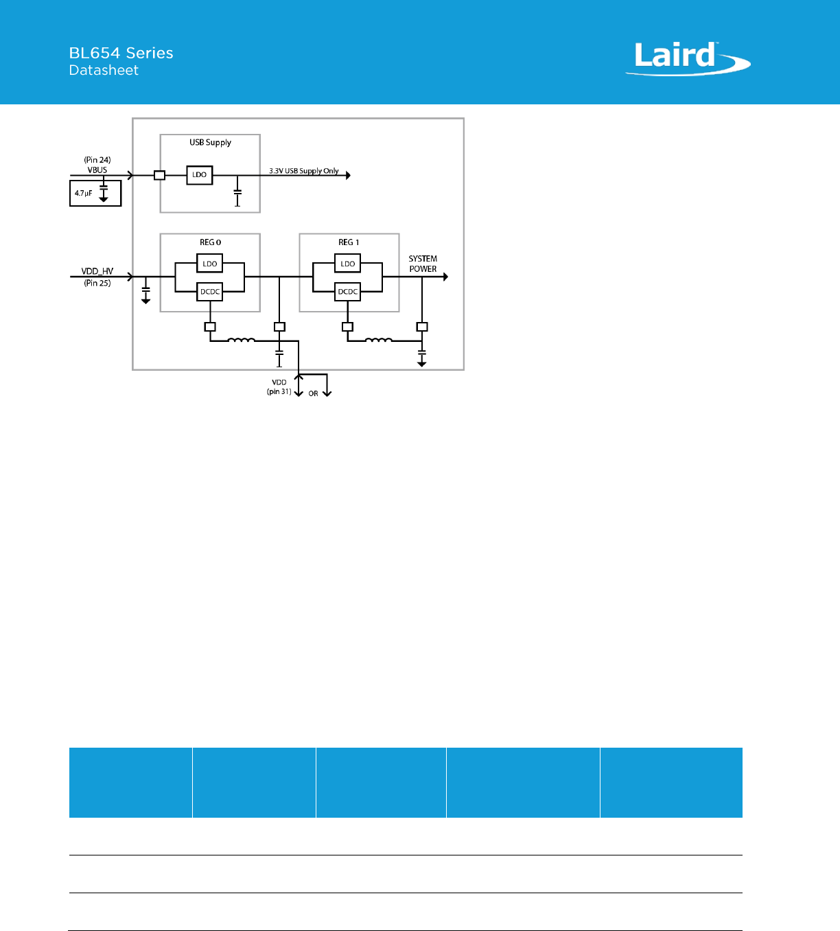
The BL654 module power supply internally contains the following two main supply regulator stages (Figure 4):
▪ REG0 – Connected to the VDD_HV pin
▪ REG1 – Connected to the VDD pin
The USB power supply is separate (connected to the VBUS pin).
Embedded Wireless Solutions Support Center:
http://ews-support.lairdtech.com
www.lairdtech.com/bluetooth
25
© Copyright 2018 Laird. All Rights Reserved
Americas: +1-800-492-2320
Europe: +44-1628-858-940
Hong Kong: +852 2923 0610
Figure 4: BL654 power supply block diagram (adapted from the following resource:
http://infocenter.nordicsemi.com/pdf/nRF52840_OPS_v0.5.1.pdf
The BL654 power supply system enters one of two supply voltage modes, normal or high voltage mode, depending on how
the external supply voltage is connected to these pins.
BL654 power supply options:
▪ Option 1 – Normal voltage power supply mode entered when the external supply voltage is connected to both the VDD
and VDD_HV pins (so that VDD equals VDD_HV). Connect external supply within range 1.7V to 3.6V range to BL654 VDD
and VDD_HV pins.
OR
▪ Option 2 – High voltage mode power supply mode (using BL654 VDD_HV pin) entered when the external supply voltage
in ONLY connected to the VDD_HV pin and the VDD pin is not connected to any external voltage supply. Connect
external supply within range 2.5V to 5.5V range to BL654 VDD_HV pin. BL654 VDD pin left unconnected.
For either option, if you use USB interface then the BL654 VBUS pin must be connected to external supply within the range
4.35V to 5.5V. When using the BL654 VBUS pin, you MUST externally fit a 4.7uF to ground.
Table 14 summarizes these power supply options.
Table 14: BL654 powering options
Power Supply Pins
and Operating
Voltage Range
OPTION1
Normal voltage
mode operation
connect?
OPTION2
High voltage mode
operation connect?
OPTION1 with USB
peripheral,
operation, and normal
voltage connect?
OPTION2 with USB
peripheral,
operation, and high
voltage connect?
VDD (pin31)
1.7V to 3.6V
Yes
(Note 1)
No
(Note 2)
Yes
No
(Note 2)
VDD_HV (pin25)
2.5V to 5.5V
No
Yes
No
Yes
(Note 5)
VBUS (pin24)
4.35V to 5.5V
No
Note 3
Yes
(Note 4)
Yes
(Note 4)
Embedded Wireless Solutions Support Center:
http://ews-support.lairdtech.com
www.lairdtech.com/bluetooth
26
© Copyright 2018 Laird. All Rights Reserved
Americas: +1-800-492-2320
Europe: +44-1628-858-940
Hong Kong: +852 2923 0610
Power Supply Option Notes:
Note 1
Option 1 – External supply voltage is connected to BOTH the VDD and VDD_HV pins (so that VDD equals
VDD_HV). Connect external supply within range 1.7V to 3.6V range to BOTH BL654 VDD and VDD_HV pins.
Note 2
Option 2 – External supply within range 2.5V to 5.5V range to the BL654 VDD_HV pin ONLY. BL654 VDD pin left
unconnected.
In High voltage mode, the VDD pin becomes an output voltage pin. It can be used to supply external circuitry
from the VDD pin. Before any current can be taken from the BL654 VDD pin, this feature must be enabled in
the BL654. Additionally, the VDD output voltage is configurable from 1.8V to 3.3V with possible settings of
1.8V, 2.1V, 2.4V, 2.7V, 3.0V, and 3.3V. The default voltage is 1.8V.
The supported BL654 VDD pin output voltage range depends on the supply voltage provided on the BL654
VDD_HV pin. The minimum difference between voltage supplied on the VDD_HV pin and the voltage output on
the VDD pin is 0.3 V. The maximum output voltage of the VDD pin is VDDH – 0.3V. Table4 shows the current
that can be drawn by external circuitry from VDD pin in high voltage mode (supply on VDD_HV).
Table 15: Current that can be drawn by external circuitry from VDD pin in High voltage mode (supply on VDDH)
Parameter
Min
Typ
Max
Unit
Current that can be drawn by external circuitry from VDD pin in
High voltage mode (supply on VDD_HV) with EXTSUPPLY enabled
in UICR during System OFF
1
mA
Current that can be drawn by external circuitry from VDD pin in
High voltage mode (supply on VDD_HV) with EXTSUPPLY enabled
in UICR during System ON
25
mA
Current drawn from VDD pin in High voltage mode (supply on
VDD_HV) of both external circuits and BL654
50
mA
Minimum difference between voltage supplied on VDD_HV pin
and voltage on VDD pin
0.3
V
Note 3
Depends on whether USB operation is required.
Note 4
When using the BL654 VBUS pin, you must externally fit a 4.7uF capacitor to ground.
Note 5
To use the BL654 USB peripheral:
1. Connect the BL654 VBUS pin to the external supply within the range 4.35V to 5.5V. When using the
BL654 VBUS pin, you MUST externally fit a 4.7uF to ground.
2. Connect the external supply to either the VDD (Option 1) or VDD_HV (Option 2) pin to operate the rest
of BL654 module.
When using the BL654 USB peripheral, the VBUS pin can be supplied from same source as VDD_HV
(within the operating voltage range of the VBUS pin and VDD_HV pin).
Embedded Wireless Solutions Support Center:
http://ews-support.lairdtech.com
www.lairdtech.com/bluetooth
27
© Copyright 2018 Laird. All Rights Reserved
Americas: +1-800-492-2320
Europe: +44-1628-858-940
Hong Kong: +852 2923 0610
The integrated high accuracy 32 MHz (±10 ppm) crystal oscillator helps with radio operation and reducing power
consumption in the active modes.
The integrated on-chip 32.768 kHz RC oscillator (±250 ppm) provides protocol timing and helps with radio power
consumption in the system StandByDoze and Deep Sleep modes by reducing the time that the RX window needs to be open.
To keep the on-chip 32.768 kHz RC oscillator within ±250 ppm (which is needed to run the BLE stack) accuracy, RC oscillator
needs to be calibrated (which takes 16-17 mS) regularly. The default calibration interval is eight seconds which is enough to
keep within ±250 ppm. The calibration interval ranges from 0.25 seconds to 31.75 seconds (in multiples of 0.25 seconds) and
configurable via firmware
When using smartBASIC, the timer subsystem enables applications to be written which allow future events to be generated
based on timeouts.
▪ Regular Timer – There are eight built-in timers (regular timers) derived from a single RTC clock which are controlled
solely by smart BASIC functions. The resolution of the regular timer is 976 microseconds.
▪ Tick Timer – A 31-bit free running counter that increments every (1) millisecond. The resolution of this counter is 488
microseconds.
Refer to the smart BASIC User Guide available from the Laird BL654 product page. For timer utilization when using the Nordic
SDK, refer to http://infocenter.nordicsemi.com/index.jsp.
▪ 2402–2480 MHz Bluetooth Low Energy radio BT5.0 – 1 Mbps, 2 Mbps, and Long-range (125 kbps and 500 kbps TBD)
over-the-air data rate.
▪ Tx output power of +8 dBm programmable to -20 dBm in steps of 4 dB and further TX power level of -40 dBm.
▪ Receiver (with integrated channel filters) to achieve maximum sensitivity -95 dBm @ 1 Mbps BLE, -92 dBm @2 Mbps, -
103 dBm @ 125 kbps long-range and TBD @500kbps long-range).
▪ RF conducted interface available in the following two ways:
–
–
▪ Antenna options:
–
–
▪ Received Signal Strength Indicator (RSSI)
RSSI accuracy (valid range -90 to -20dBm) is -2dB typical
RSSI resolution 1dB typical
NFC support:
▪ Based on the NFC forum specification
–
–
–
▪ Modes of operation:
Embedded Wireless Solutions Support Center:
http://ews-support.lairdtech.com
www.lairdtech.com/bluetooth
28
© Copyright 2018 Laird. All Rights Reserved
Americas: +1-800-492-2320
Europe: +44-1628-858-940
Hong Kong: +852 2923 0610
–
–
–
▪ Touch-to Pair with NFC
▪ Launch a smartphone app (on Android)
▪ NFC enabled Out-of-Band Pairing
▪ System Wake-On-Field function
–
Table 16: NFC interface
Signal Name
Pin No
I/O
Comments
NFC1/SIO_09
59
I/O
The NFC pins are by default NFC pins and an alternate function on each pin
is GPIO. Refer to the smartBASIC. User manual.
NFC2/SIO_10
57
I/O
From Nordic’s nRF52840 Objective Product Specification v0.5.1
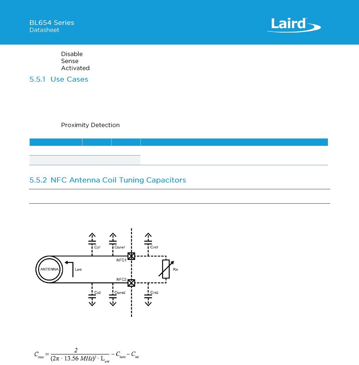
The NFC antenna coil must be the connected differential between the NFC1 and NFC2 pins of the BL654. Two external
capacitors should be used to tune the resonance of the antenna circuit to 13.56 MHz (Figure 5).
Figure 5: NFC antenna coil tuning capacitors
The required external tuning capacitor value is given by the following equations:
An antenna inductance of Lant = 0.72 uH provides tuning capacitors in the range of 300 pF on each pin. The total capacitance
on NFC1 and NFC2 must be matched. Cint and Cp are small usually (Cint is 4pF), so can omit from calculation.
Embedded Wireless Solutions Support Center:
http://ews-support.lairdtech.com
www.lairdtech.com/bluetooth
29
© Copyright 2018 Laird. All Rights Reserved
Americas: +1-800-492-2320
Europe: +44-1628-858-940
Hong Kong: +852 2923 0610
From Nordic’s nRF52840 Objective Product Specification v0.5.1
If the NFC coil antenna is exposed to a strong NFC field, the supply current may flow in the opposite direction due to parasitic
diodes and ESD structures.
If the used battery does not tolerate a return current, a series diode must be placed between the battery and the BL654 to
protect the battery.
Note: The BL654 has two UARTs.
The Universal Asynchronous Receiver/Transmitter (UART) offers fast, full-duplex, asynchronous serial communication with
built-in flow control support (UART_CTS, UART_RTS) in HW up to one Mbps baud. Parity checking and generation for the
ninth data bit are supported.
UART_TX, UART_RX, UART_RTS, and UART_CTS form a conventional asynchronous serial data port with handshaking. The
interface is designed to operate correctly when connected to other UART devices such as the 16550A. The signaling levels are
nominal 0 V and 3.3 V (tracks VDD) and are inverted with respect to the signaling on an RS232 cable.
Two-way hardware flow control is implemented by UART_RTS and UART_CTS. UART_RTS is an output and UART_CTS is an
input. Both are active low.
These signals operate according to normal industry convention. UART_RX, UART_TX, UART_CTS, UART_RTS are all 3.3 V level
logic (tracks VDD). For example, when RX and TX are idle they sit at 3.3 V. Conversely for handshaking pins CTS, RTS at 0 V is
treated as an assertion.
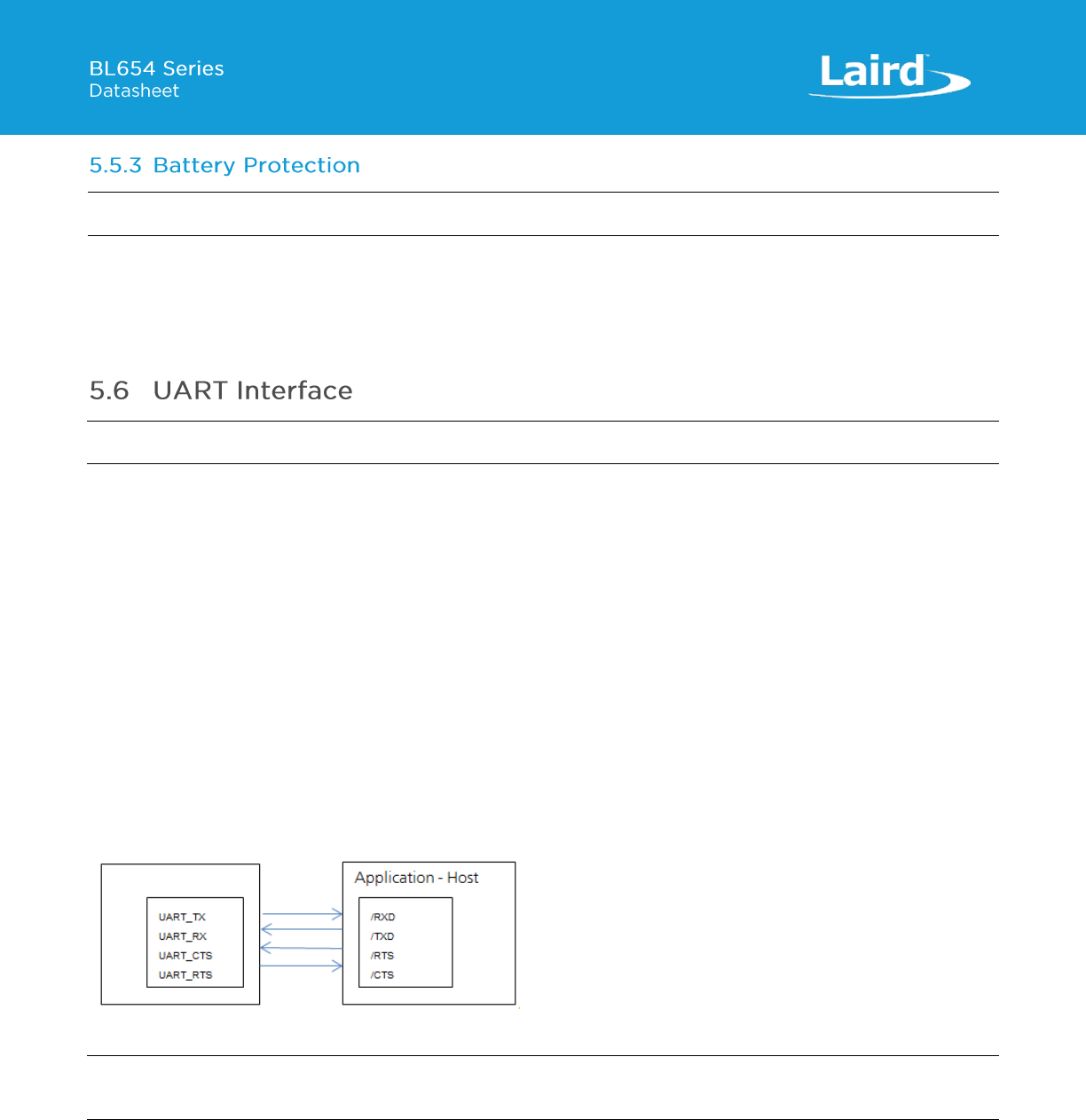
The module communicates with the customer application using the following signals:
▪ Port/TxD of the application sends data to the module’s UART_RX signal line
▪ Port/RxD of the application receives data from the module’s UART_TX signal line
Figure 6: UART signals
Note: The BL654 serial module output is at 3.3V CMOS logic levels (tracks VDD). Level conversion must be added to
interface with an RS-232 level compliant interface.
Some serial implementations link CTS and RTS to remove the need for handshaking. We do not recommend linking CTS and
RTS other than for testing and prototyping. If these pins are linked and the host sends data at the point that the BL654
deasserts its RTS signal, there is significant risk that internal receive buffers will overflow, which could lead to an internal
processor crash. This will drop the connection and may require a power cycle to reset the module. We recommend that the
correct CTS/RTS handshaking protocol be adhered to for proper operation.
BL654
Embedded Wireless Solutions Support Center:
http://ews-support.lairdtech.com
www.lairdtech.com/bluetooth
30
© Copyright 2018 Laird. All Rights Reserved
Americas: +1-800-492-2320
Europe: +44-1628-858-940
Hong Kong: +852 2923 0610
Table 17: UART interface
Signal Name
Pin No
I/O
Comments
SIO_06 / UART_Tx
35
O
SIO_06 (alternative function UART_Tx) is an output, set high
(in firmware).
SIO_08 / UART_Rx
29
I
SIO_08 (alternative function UART_Rx) is an input, set with internal
pull-up (in firmware).
SIO_05 / UART_RTS
39
O
SIO_05 (alternative function UART_RTS) is an output, set low
(in firmware).
SIO_07 / UART_CTS
37
I
SIO_07 (alternative function UART_CTS) is an input, set with internal
pull-down (in firmware).
The UART interface is also used to load customer developed smartBASIC application script.
The BL654 has two UARTs.
BL654 has USB2.0 FS (Full Speed, 12Mbps) hardware capability. There is a CDC driver/Virtual UART (baud rate TBD) as well as
other USB drivers available via Nordic SDK – such as: usb_audio, usb_hid, usb_generic, usb_msc (mass storage device).
Table 18: USB interface
Signal Name
Pin No
I/O
Comments
D-
17
I/O
D+
15
I/O
VBUS
24
When using the BL654 VBUS pin (which is mandatory when USB interface is used),
Customer MUST connect externally a 4.7uF capacitor to ground.
Note: You MUST power the rest of BL654 module circuitry through the VDD pin
(OPTION1) or VDD_HV pin (OPTION2).
The SPI interface is an alternate function on SIO pins.
The module is a master device that uses terminals SPI_MOSI, SPI_MISO, and SPI_CLK. SPI_CS is implemented using any spare
SIO digital output pins to allow for multi-dropping.
The SPI interface enables full duplex synchronous communication between devices. It supports a 3-wire (SPI_MOSI,
SPI_MISO, SPI_SCK,) bidirectional bus with fast data transfers to and from multiple slaves. Individual chip select signals are
necessary for each of the slave devices attached to a bus, but control of these is left to the application through use of SIO
signals. I/O data is double-buffered.
The SPI peripheral supports SPI mode 0, 1, 2, and 3.
Table 19: SPI interfaces
Signal Name
Pin No
I/O
Comments
SIO_45/SPI_MOSI
56
O
This interface is an alternate function configurable by
smartBASIC. Default in the FW pin 56 and 53 are SIO inputs. SPIOPEN() in
smartBASIC selects SPI function and changes pin 56 and 53 to outputs (when in
SPI master mode).
SIO_46/SPI_MISO
51
I
SIO_47/SPI_CLK
53
O
Any_SIO/SPI_CS
54
I
SPI_CS is implemented using any spare SIO digital output pins to allow for multi-
dropping. On Laird devboard SIO_44 (pin54) used as SPI_CS.
Embedded Wireless Solutions Support Center:
http://ews-support.lairdtech.com
www.lairdtech.com/bluetooth
31
© Copyright 2018 Laird. All Rights Reserved
Americas: +1-800-492-2320
Europe: +44-1628-858-940
Hong Kong: +852 2923 0610
The I2C interface is an alternate function on SIO pins.
The two-wire interface can interface a bi-directional wired-OR bus with two lines (SCL, SDA) and has master /slave topology.
The interface is capable of clock stretching. Data rates of 100 kbps and 400 kbps are supported.
An I2C interface allows multiple masters and slaves to communicate over a shared wired-OR type bus consisting of two lines
which normally sit at VDD. The SCL is the clock line which is always sourced by the master and SDA is a bi-directional data line
which can be driven by any device on the bus.
IMPORTANT: It is essential to remember that pull-up resistors on both SCL and SDA lines are not provided in the
module and MUST be provided external to the module.
Table 20: I2C interface
Signal Name
Pin No
I/O
Comments
SIO_26/I2C_SDA
36
I/O
This interface is an alternate function on each pin, configurable by
smartBASIC. I2COPEN() in smartBASIC selects I2C function.
SIO_27/I2C_SCL
38
I/O
The 19 SIO pins are configurable by smartBASIC application script or Nordic SDK. They can be accessed individually. Each has
the following user configured features:
▪ Input/output direction
▪ Output drive strength (standard drive 0.5 mA or high drive 5mA)
▪ Internal pull-up and pull-down resistors (13 K typical) or no pull-up/down or input buffer disconnect
▪ Wake-up from high or low-level triggers on all pins including NFC pins
The ADC is an alternate function on SIO pins, configurable by smart BASIC or Nordic SDK.
The BL654 provides access to 8-channel 8/10/12-bit successive approximation ADC in one-shot mode. This enables sampling
up to 8 external signals through a front-end MUX. The ADC has configurable input and reference pre-scaling and sample
resolution (8, 10, and 12 bit).
Table 21: Analog interface
Signal Name
Pin No
I/O
Comments
SIO_05/UART_RTS/AIN3 – Analog Input
39
I
This interface is an alternate function on each pin,
configurable by smartBASIC. AIN configuration
selected using GpioSetFunc() function.
Configurable 8, 10, 12-bit resolution.
Configurable voltage scaling 4, 2, 1/1, 1/3, 1/3, 1/4,
1/5, 1/6(default).
Configurable acquisition time 3uS, 5uS, 10uS(default),
15uS, 20uS, 40uS.
Full scale input range (VDD)
SIO_04/AIN2 – Analog Input
34
I
SIO_03/AIN1 – Analog Input
49
I
SIO_02/AIN0 – Analog Input
50
I
SIO_31/AIN7 – Analog Input
44
I
SIO_30/AIN6 – Analog Input
45
I
SIO_29/AIN5 – Analog Input
48
I
SIO_28/AIN4 – Analog Input
46
I
Embedded Wireless Solutions Support Center:
http://ews-support.lairdtech.com
www.lairdtech.com/bluetooth
32
© Copyright 2018 Laird. All Rights Reserved
Americas: +1-800-492-2320
Europe: +44-1628-858-940
Hong Kong: +852 2923 0610
The PWM output is an alternate function on ALL (GPIO) SIO pins, configurable by smartBASIC or the Nordic SDK.
The PWM output signal has a frequency and duty cycle property. Frequency is adjustable (up to 1 MHz) and the duty cycle
can be set over a range from 0% to 100%.
PWM output signal has a frequency and duty cycle property. PWM output is generated using dedicated hardware in the
chipset. There is a trade-off between PWM output frequency and resolution.
For example:
▪ PWM output frequency of 500 kHz (2 uS) results in resolution of 1:2.
▪ PWM output frequency of 100 kHz (10 uS) results in resolution of 1:10.
▪ PWM output frequency of 10 kHz (100 uS) results in resolution of 1:100.
▪ PWM output frequency of 1 kHz (1000 uS) results in resolution of 1:1000.
The FREQ output is an alternate function on 16 (GPIO) SIO pins, configurable by smartBASIC or Nordic SDK.
Note: The frequency driving each of the 16 SIO pins is the same but the duty cycle can be independently set for each pin.
FREQ output signal frequency can be set over a range of 0Hz to 4 MHz (with 50% mark-space ratio).
Table 22: nRESET pin
Signal Name
Pin No
I/O
Comments
nRESET
19
I
BL654 HW reset (active low). Pull the nRESET pin low for minimum 100mS
for the BL654 to reset.
The BL654 Firmware hex file consists of four elements:
▪ smartBASIC runtime engine
▪ Nordic Softdevice
▪ Master Bootloader
Laird BL654 smartBASIC firmware (FW) image part numbers are referenced as w.x.y.z (ex. v29.x.y.z). The BL654 smartBASIC
runtime engine and Softdevice combined image can be upgraded by the customer over the UART interface.
You also have the option to use the two-wire (JTAG) interface, during production, to clone the file system of a Golden
preconfigured BL654 to others using the Flash Cloning process. This is described in the following application note Flash
Cloning for the BL654. In this case the file system is also part of the .hex file.
Signal Name
Pin No
I/O
Comments
SWDIO
1
I/O
Internal pull-up resistor
SWDCLK
3
I
Internal pull-down resistor
The Laird development board incorporates an on-board JTAG J-link programmer for this purpose. There is also the following
JTAG connector which allows on-board JTAG J-link programmer signals to be routed off the development board. The only
requirement is that you should use the following JTAG connector on the host PCB.
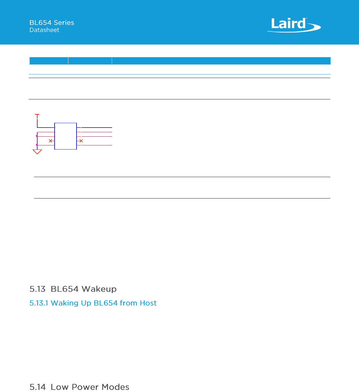
Embedded Wireless Solutions Support Center:
http://ews-support.lairdtech.com
www.lairdtech.com/bluetooth
33
© Copyright 2018 Laird. All Rights Reserved
Americas: +1-800-492-2320
Europe: +44-1628-858-940
Hong Kong: +852 2923 0610
The JTAG connector MPN is as follows:
Reference
Part
Description and MPN (Manufacturers Part Number)
JP1
FTSH-105
Header, 1.27mm, SMD, 10-way, FTSH-105-01-L-DV Samtech
Note: Reference on the BL654 development board schematic (Figure 7) shows the DVK development schematic wiring
only for the JTAG connector and the BL654 module JTAG pins.
Figure 7: BL654 development board schematic
Note: The BL654 development board allows Laird on-board JTAG J-link programmer signals to be routed off the
development board by from connector JP1
JTAG is require because Nordic SDK applications can only be loaded using the JTAG (smartBASIC firmware can be loaded using
JTAG as well as over the UART). We recommend that you use JTAG (2-wire interface) to handle future BL654 module
firmware upgrades. You must wire out the JTAG (2-wire interface) on your host design (see Figure 7, where the following four
lines should be wired out – SWDIO, SWDCLK, GND and VCC). smartBASIC firmware upgrades can still be performed over the
BL654 UART interface, but this is slower than using the BL654 JTAG (2-wire interface) – (60 seconds using UART vs. 10
seconds when using JTAG).
SWO (SIO_32) is a Trace output (called SWO, Serial Wire Output) and is not necessary for programming BL654 over the SWD
interface.
nRESET_BLE is not necessary for programming BL654 over the SWD interface.
Wake the BL654 from the host using wake-up pins (any SIO pin). You may configure the BL654’s wakeup pins via smartBASIC
to do any of the following:
▪ Wake up when signal is low
▪ Wake up when signal is high
▪ Wake up when signal changes
Refer to the smartBASIC user guide for details. You can access this guide from the Laird BL654 product page.
For BL654 wake-up using the Nordic SDK, refer to Nordic infocenter.nordicsemi.com.
The BL654 has three power modes: Run, Standby Doze, and Deep Sleep.
The module is placed automatically in Standby Doze if there are no pending events (when WAITEVENT statement is
encountered within a customer’s smartBASIC script). The module wakes from Standby Doze via any interrupt (such as a
GND
SWDIO_EXT
SWDCLK_EXT
JP1
PIN HEADER,1.27mm 2X5P
1 2
3 4
5 6
7 8
910 nRESET_EXT
SWO_EXT
VDD_VSRC_nRF
Embedded Wireless Solutions Support Center:
http://ews-support.lairdtech.com
www.lairdtech.com/bluetooth
34
© Copyright 2018 Laird. All Rights Reserved
Americas: +1-800-492-2320
Europe: +44-1628-858-940
Hong Kong: +852 2923 0610
received character on the UART Rx line). If the module receives a UART character from either the external UART or the radio,
it wakes up.
Deep sleep is the lowest power mode. Once awakened, the system goes through a system reset.
For different Nordic power modes using the Nordic SDK, refer to Nordic infocenter.nordicsemi.com.
The on-silicon temperature sensor has a temperature range greater than or equal to the operating temperature of the device.
Resolution is 0.25°C degrees. The on-silicon temperature sensor accuracy is ±5°C.
To read temperature from on-silicon temperature sensor (in tenth of centigrade, so 23.4°C is output as 234) using smartBASIC:
▪ In command mode, use ATI2024
or
▪ From running a smartBASIC application script, use SYSINFO(2024)
Exposed via an API in smartBASIC (see smartBASIC documentation available from the BL654 product page). The rand()
function from a running smartBASIC application returns a value.
For Nordic related functionality, visit Nordic infocenter.nordicsemi.com
Exposed via an API in smartBASIC (see smartBASIC documentation available from the BL654 product page). Function called
aesencrypt and aesdecrypt.
For Nordic related functionality, visit Nordic infocenter.nordicsemi.com
ARM Cryptocell incorporates a true random generator (TRNG) and support for a wide range of asymmetric, symmetric and
hashing cryptographic services for secure applications. For more information, please check the Nordic SDK.
The BL654 supports readback protection capability that disallows the reading of the memory on the nrf52840 using a JTAG
interface. Available via smartBASIC or the Nordic SDK.
The BL654 offers a range of functions for generating public/private keypair, calculating a shared secret, as well as generating
an authenticated hash. Available via smartBASIC or the Nordic SDK.
This is not required for normal BL654 module operation.
The BL654 uses the on-chip 32.76 kHz RC oscillator (LFCLK) by default (which has an accuracy of ±250 ppm) which requires
regulator calibration (every eight seconds) to within ±250 ppm.
You can connect an optional external high accuracy (±20 ppm) 32.768 kHz crystal (and associated load capacitors) to the
BL654SIO_01/XL2 (pin 41) and SIO_00/XL1 (pin 42) to provide improved protocol timing and to help with radio power
Embedded Wireless Solutions Support Center:
http://ews-support.lairdtech.com
www.lairdtech.com/bluetooth
35
© Copyright 2018 Laird. All Rights Reserved
Americas: +1-800-492-2320
Europe: +44-1628-858-940
Hong Kong: +852 2923 0610
consumption in the system standby doze/deep sleep modes by reducing the time that the RX window needs to be open.
Table 23 compares the current consumption difference between RC and crystal oscillator.
Table 23: Comparing current consumption difference between BL654 on-chip RC 32.76 kHz oscillator and optional external crystal
(32.768kHz) based oscillator
BL654 On-chip 32.768 kHz RC Oscillator
(±250 ppm) LFRC
Optional External Higher Accuracy (±20
ppm) 32.768 kHz Crystal-based Oscillator XO
Current Consumption of
32.768 kHz Block
TBD uA
TBD uA
Standby Doze Current
TBD uA
TBD uA
Calibration
Calibration required regularly (default eight
seconds interval).
Calibration takes 16-17 ms; with DCDC used,
the total charge of a calibration event is TBD
uC.
The average current consumed by the
calibration depends on the calibration
interval and can be calculated using the
following formula:
CAL_charge/CAL_interval – The lowest
calibration interval (0.25 seconds) provides an
average current of (DCDC enabled):
TBDuC/0.25s = TBDuA
To get the 250-ppm accuracy, the BLE stack
specification states that a calibration interval
of eight seconds is enough. This gives an
average current of:
TBDuC/8s = TBD uA
Added to the LFRC run current and Standby
Doze (IDLE) base current shown above results
in a total average current of:
LFRC + CAL = TBD + TBD = TBDuA
Not applicable
Total
TBD uA
TBD uA
Summary
▪ Low current consumption
▪ Accuracy 250 ppm
▪ Lowest current consumption
▪ Needs external crystal
▪ High accuracy (depends on the crystal,
usually 20 ppm)
Table 24: Optional external 32.768 kHz crystal specification
Optional external 32.768kHz crystal
Min
Typ
Max
Crystal Frequency
-
32.768 kHz
-
Frequency tolerance requirement of BLE stack
-
-
±250 ppm
Load Capacitance
-
-
12.5 pF
Shunt Capacitance
-
-
2 pF
Equivalent series resistance
-
-
100 kOhm
Drive level
-
-
1 uW
Embedded Wireless Solutions Support Center:
http://ews-support.lairdtech.com
www.lairdtech.com/bluetooth
36
© Copyright 2018 Laird. All Rights Reserved
Americas: +1-800-492-2320
Europe: +44-1628-858-940
Hong Kong: +852 2923 0610
Optional external 32.768kHz crystal
Min
Typ
Max
Input capacitance on XL1 and XL2 pads
-
4 pF
-
Run current for 32.768 kHz crystal based oscillator
-
0.25 uA
-
Start-up time for 32.768 kHz crystal based oscillator
-
0.25 seconds
-
Peak to peak amplitude for external low swing clock input signal
must not be outside supply rails
200 mV
-
1000 mV
Be sure to tune the load capacitors on the board design to optimize frequency accuracy (at room temperature) so it matches
that of the same crystal standalone, Drive Level (so crystal operated within safe limits) and oscillation margin (Rneg is at least 3
to 5 times ESR) over the operating temperature range.
The 451-00001 on-board PCB trace monopole antenna radiated performance depends on the host PCB layout.
The BL654 development board was used for BL654 development and the 451-00001 PCB antenna performance evaluation. To
obtain similar performance, follow guidelines in section PCB Layout on Host PCB for the 451-00001 to allow the on-board
antenna to radiate and reduce proximity effects due to nearby host PCB GND copper or metal covers.
Unit in dBi @2.44GHz
XY-plane
XZ-plane
YZ-plane
Efficiency
Peak
Avg
Peak
Avg
Peak
Avg
PCB trace antenna
TBD
TBD
TBD
TBD
TBD
TBD
◆XY-plane ◆XZ-plane ◆YZ-plane
The BL654 is easy to integrate, requiring no external components on your board apart from those which you require for
development and in your end application.
The following are suggestions for your design for the best performance and functionality.
Checklist (for Schematic):
▪ BL654 power supply options:
OR
OPTION2. High voltage mode power supply mode (using BL654 VDDH pin) entered when the external supply voltage in
ONLY connected to the VDDH pin and the VDD pin is not connected to any external voltage supply. Connect external
supply within range 2.5V to 5.5V range to BL654 VDDH pin. BL654 VDD pin left unconnected.
External power source should be within the operating range, rise time and noise/ripple specification of the BL654. Add
decoupling capacitors for filtering the external source. Power-on reset circuitry within BL654 series module incorporates
Embedded Wireless Solutions Support Center:
http://ews-support.lairdtech.com
www.lairdtech.com/bluetooth
37
© Copyright 2018 Laird. All Rights Reserved
Americas: +1-800-492-2320
Europe: +44-1628-858-940
Hong Kong: +852 2923 0610
brown-out detector, thus simplifying your power supply design. Upon application of power, the internal power-on reset
ensures that the module starts correctly.
▪ VDD and coin-cell operation
With a built-in DCDC (operating range 1.7V to 3.6V), that reduces the peak current required from a coin-cell, making it
easier to use with a coin-cell.
▪ AIN (ADC) and SIO pin IO voltage levels
BL654 SIO voltage levels are at VDD. Ensure input voltage levels into SIO pins are at VDD also (if VDD source is a battery
whose voltage will drop). Ensure ADC pin maximum input voltage for damage is not violated.
▪ AIN (ADC) impedance and external voltage divider setup
If you need to measure with ADC a voltage higher than 3.6V, you can connect a high impedance voltage divider to lower
the voltage to the ADC input pin.
▪ JTAG
This is REQUIRED as Nordic SDK applications can only be loaded using the JTAG (smartBASIC firmware can be loaded
using the JTAG as well as the UART).
Laird recommends you use JTAG (2-wire interface) to handle future BL654 module firmware upgrades. You MUST wire
out the JTAG (2-wire interface) on your host design (see Figure 7, where four lines should be wired out, namely SWDIO,
SWDCLK, GND and VCC). Firmware upgrades can still be performed over the BL654 UART interface, but this is slower (60
seconds using UART vs. 10 seconds when using JTAG) than using the BL654 JTAG (2-wire interface).
JTAG may be used if you intend to use Flash Cloning during production to load smartBASIC scripts.
▪ UART
Required for loading your smartBASIC application script during development (or for subsequent firmware upgrades
(except JTAG for FW upgrades and/or Flash Cloning of the smartBASIC application script). Add connector to allow
interfacing with UART via PC (UART–RS232 or UART-USB).
▪ UART_RX and UART_CTS
SIO_08 (alternative function UART_RX) is an input, set with internal weak pull-up (in firmware). The pull-up prevents the
module from going into deep sleep when UART_RX line is idling.
SIO_07 (alternative function UART_CTS) is an input, set with internal weak pull-down (in firmware). This pull-down
ensures the default state of the UART_CTS will be asserted which means can send data out of the UART_TX line. Laird
recommends that UART_CTS be connected.
▪ nAutoRUN pin and operating mode selection
nAutoRUN pin needs to be externally held high or low to select between the two BL654 operating modes at power-up:
–
–
▪ I2C
It is essential to remember that pull-up resistors on both I2C_SCL and I2C_SDA lines are not provided in the BL654
module and MUST be provided external to the module as per I2C standard.
▪ SPI
Implement SPI chip select using any unused SIO pin within your smartBASIC application script or Nordic application then
SPI_CS is controlled from the software application allowing multi-dropping.
▪ SIO pin direction
BL654 modules shipped from production with smart BASIC FW, all SIO pins (with default function of DIO) are mostly
digital inputs (see Pin Definitions Table2). Remember to change the direction SIO pin (in your smartBASIC application
script) if that particular pin is wired to a device that expects to be driven by the BL654 SIO pin configured as an output.
Also, these SIO pins have the internal pull-up or pull-down resistor-enabled by default in firmware (see Pin Definitions
Table 2). This was done to avoid floating inputs, which can cause current consumption in low power modes (e.g.
StandbyDoze) to drift with time. You can disable the PULL-UP or Pull-down through their smartBASIC application.
Embedded Wireless Solutions Support Center:
http://ews-support.lairdtech.com
www.lairdtech.com/bluetooth
38
© Copyright 2018 Laird. All Rights Reserved
Americas: +1-800-492-2320
Europe: +44-1628-858-940
Hong Kong: +852 2923 0610
Note: Internal pull-up, pull down will take current from VDD.
▪ SIO_02 pin and OTA smartBASIC application download feature
SIO_02 is an input, set with internal pull-down (in FW). Refer to latest firmware release documentation on how SIO_02
is used for Over the Air smartBASIC application download feature. The SIO_02 pin must be pulled high externally to
enable the feature. Decide if this feature is required in production. When SIO_02 is high, ensure nAutoRun is NOT high
at same time; otherwise you cannot load the smartBASIC application script.
• NFC antenna connector
To make use of the Laird flexi-PCB NFC antenna, fit connector:
Description: FFC/FPC Connector, Right Angle, SMD/90d, Dual Contact,1.2 mm Mated Height
Manufacturer: Molex
Manufacturers Part number: 512810594
Add tuning capacitors of 300 pF on NFC1 pin to GND and 300 pF on NFC2 pins to GND if the PCB track length is similar as
development board.
▪ nRESET pin (active low)
Hardware reset. Wire out to push button or drive by host.
By default module is out of reset when power applied to VCC pins.
▪ Optional External 32.768kHz crystal
If the optional external 32.768kHz crystal is needed then use a crystal that meets specification and add load capacitors
whose values should be tuned to meet all specification for frequency and oscillation margin.
▪ SIO_38 special function pin
This is for future use by Laird. It is currently a Do Not Connect pin.
Checklist (for PCB):
▪ MUST locate BL654 module close to the edge of PCB (mandatory for the 451-00001 for on-board PCB trace antenna to
radiate properly).
▪ Use solid GND plane on inner layer (for best EMC and RF performance).
▪ All module GND pins MUST be connected to host PCB GND.
▪ Place GND vias close to module GND pads as possible.
▪ Unused PCB area on surface layer can flooded with copper but place GND vias regularly to connect the copper flood to
the inner GND plane. If GND flood copper is on the bottom of the module, then connect it with GND vias to the inner
GND plane.
▪ Route traces to avoid noise being picked up on VDD, VDDH, VBUS supply and AIN (analogue) and SIO (digital) traces.
▪ Ensure no exposed copper is on the underside of the module (refer to land pattern of BL654 development board).
The 451-00001 has an integrated PCB trace antenna and its performance is sensitive to host PCB. It is critical to locate the
451-00001 on the edge of the host PCB (or corner) to allow the antenna to radiate properly. Refer to guidelines in section
PCB land pattern and antenna keep-out area for the 451-00001. Some of those guidelines repeated below.
▪ Ensure there is no copper in the antenna keep-out area on any layers of the host PCB. Keep all mounting hardware and
metal clear of the area to allow proper antenna radiation.
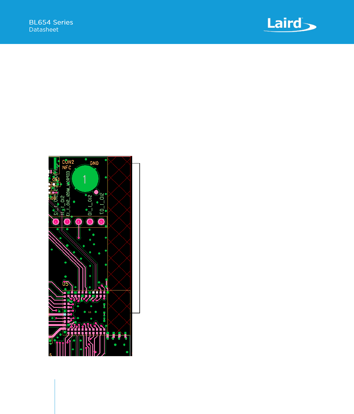
Embedded Wireless Solutions Support Center:
http://ews-support.lairdtech.com
www.lairdtech.com/bluetooth
39
© Copyright 2018 Laird. All Rights Reserved
Americas: +1-800-492-2320
Europe: +44-1628-858-940
Hong Kong: +852 2923 0610
▪ For best antenna performance, place the 451-00001 module on the edge of the host PCB, preferably in the corner with
the antenna facing the corner.
▪ The BL654 development board has the 451-00001 module on the edge of the board (not in the corner). The antenna
keep-out area is defined by the BL654 development board which was used for module development and antenna
performance evaluation is shown in Figure 8, where the antenna keep-out area is ~TBD mm wide, TBD mm long; with
PCB dielectric (no copper) height 0.85 mm sitting under the 451-00001 PCB trace antenna.
▪ The 451-00001 PCB trace antenna is tuned when the 451-00001 is sitting on development board (host PCB) with size of
125 mm x 85 mm.
▪ A different host PCB thickness dielectric will have small effect on antenna.
▪ The antenna-keep-out defined in the Host PCB Land Pattern and Antenna Keep-out for the 451-00001 section.
▪ Host PCB land pattern and antenna keep-out for the BL654 applies when the 451-00001 is placed in the corner of the
host PCB. When the 451-00001 cannot be placed as such, it must be placed on the edge of the host PCB and the
antenna keep out must be observed. Figure 8 shows an example.
Figure 8: PCB trace Antenna keep-out area (shown in red), corner of the BL654 development board for the 451-00001 module.
Antenna Keep-out Notes:
Note 1
The BL654 module is placed on the edge of the host PCB.
Note 2
Copper cut-away on all layers in the Antenna Keep-out area under the 451-00001 on host PCB.
Antenna Keep-out
Embedded Wireless Solutions Support Center:
http://ews-support.lairdtech.com
www.lairdtech.com/bluetooth
40
© Copyright 2018 Laird. All Rights Reserved
Americas: +1-800-492-2320
Europe: +44-1628-858-940
Hong Kong: +852 2923 0610
Checklist (for metal /plastic enclosure):
▪ Minimum safe distance for metals without seriously compromising the antenna (tuning) is 40 mm top/bottom and 30
mm left or right.
▪ Metal close to the 451-00001 PCB trace monopole antenna (bottom, top, left, right, any direction) will have degradation
on the antenna performance. The amount of that degradation is entirely system dependent, meaning you will need to
perform some testing with your host application.
▪ Any metal closer than 20 mm will begin to significantly degrade performance (S11, gain, radiation efficiency).
▪ It is best that you test the range with a mock-up (or actual prototype) of the product to assess effects of enclosure
height (and materials, whether metal or plastic).
Please refer to the regulatory sections for FCC, IC, CE, and Japan for details of use of BL654-with external antennas in each
regulatory region.
The BL654 family has been designed to operate with the below external antennas (with a maximum gain of
2.0 dBi). The required antenna impedance is 50 ohms. See Table 25. External antennas improve radiation efficiency.
Table 25: External antennas for the BL654
Manufacturer
Model
Laird
Part Number
Type
Connector
Peak Gain
2400-2500 MHz
2400-2480 MHz
Laird
NanoBlue
TBD
PCB Dipole
IPEX MHF4
2 dBi
-
Laird
FlexPIFA
001-0022
PCB Dipole
IPEX MHF4
-
2 dBi
Laird
FlexNotch
001-0023
PCB Dipole
IPEX MHF4
-
2 dBi
Mag.Layers
EDA-8709-2G4C1-B27-CY
0600-00057
Dipole
IPEX MHF4
2 dBi
-
Laird
mFlexPIFA
EFA2400A3S-10MH4L
PIFA
IPEX MHF4
-
2 dBi
Laird
Laird NFC
0600-00061
NFC
N/A
-
-
Laird
BL654-SA PCB printed antenna
NA
Printed PCB
N/A
0 dBi
-
Walsin
RFDPA870900SBAB8G1
NA
Dipole
SMA
2dBi
Embedded Wireless Solutions Support Center:
http://ews-support.lairdtech.com
www.lairdtech.com/bluetooth
41
© Copyright 2018 Laird. All Rights Reserved
Americas: +1-800-492-2320
Europe: +44-1628-858-940
Hong Kong: +852 2923 0610
Figure 9: BL654 mechanical drawings
Development Kit Schematics can be found in the software downloads tab of the BL654 product page:
TBC
Rear View
Embedded Wireless Solutions Support Center:
http://ews-support.lairdtech.com
www.lairdtech.com/bluetooth
42
© Copyright 2018 Laird. All Rights Reserved
Americas: +1-800-492-2320
Europe: +44-1628-858-940
Hong Kong: +852 2923 0610
Figure 10: Land pattern and Keep-out for the 451-00001
All dimensions are in mm.
Host PCB Land Pattern and Antenna Keep-out for the 451-00001 Notes:
Note 1
Ensure there is no copper in the antenna ‘keep out area’ on any layers of the host PCB. Also keep all mounting
hardware or any metal clear of the area (Refer to 6.3.2) to reduce effects of proximity detuning the antenna
and to help antenna radiate properly.
Note 2
For the best on-board antenna performance, the module 451-00001 MUST be placed on the edge of the host
PCB and preferably in the corner with the antenna facing the corner. Above “Keep Out Area” is the module
placed in corner of PCB. If the 451-00001 is not placed in corner but on edge of host PCB, the antenna “Keep
Out Area” is extended (see Note 4).
Note 3
BL654 development board has the 451-00001 placed on the edge of the PCB board (and not in corner) for that
the Antenna keep out area is extended down to the corner of the development board, see section PCB Layout
on Host PCB for the 451-00001, Figure 10. This was used for module development and antenna performance
evaluation.
Note 4
Ensure that there is no exposed copper under the module on the host PCB.
Note 5
You may modify the PCB land pattern dimensions based on their experience and/or process capability.
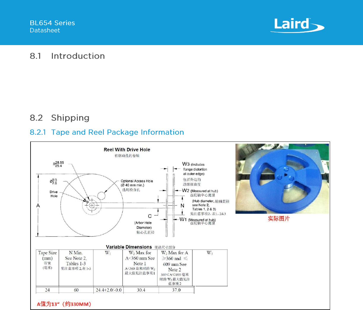
Embedded Wireless Solutions Support Center:
http://ews-support.lairdtech.com
www.lairdtech.com/bluetooth
43
© Copyright 2018 Laird. All Rights Reserved
Americas: +1-800-492-2320
Europe: +44-1628-858-940
Hong Kong: +852 2923 0610
Laird Technologies surface mount modules are designed to conform to all major manufacturing guidelines. This application
note is intended to provide additional guidance beyond the information that is presented in the User Manual. This
Application Note is considered a living document and will be updated as new information is presented.
The modules are designed to meet the needs of several commercial and industrial applications. They are easy to manufacture
and conform to current automated manufacturing processes.
Figure 11: Reel specifications
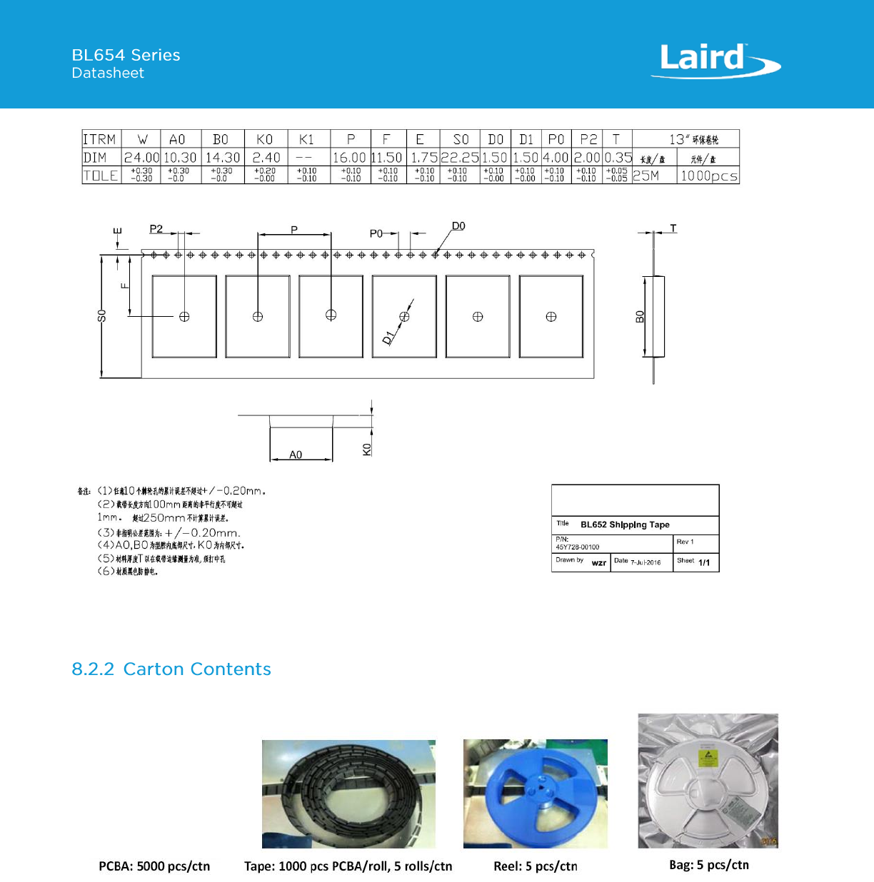
Embedded Wireless Solutions Support Center:
http://ews-support.lairdtech.com
www.lairdtech.com/bluetooth
44
© Copyright 2018 Laird. All Rights Reserved
Americas: +1-800-492-2320
Europe: +44-1628-858-940
Hong Kong: +852 2923 0610
Figure 12: Tape specifications
There are 1,000 x BL654 modules taped in a reel (and packaged in a pizza box) and five boxes per carton (5000 modules per
carton). Reel, boxes, and carton are labeled with the appropriate labels. See Carton Contents for more information.
The following are the contents of the carton shipped for the BL654 modules.
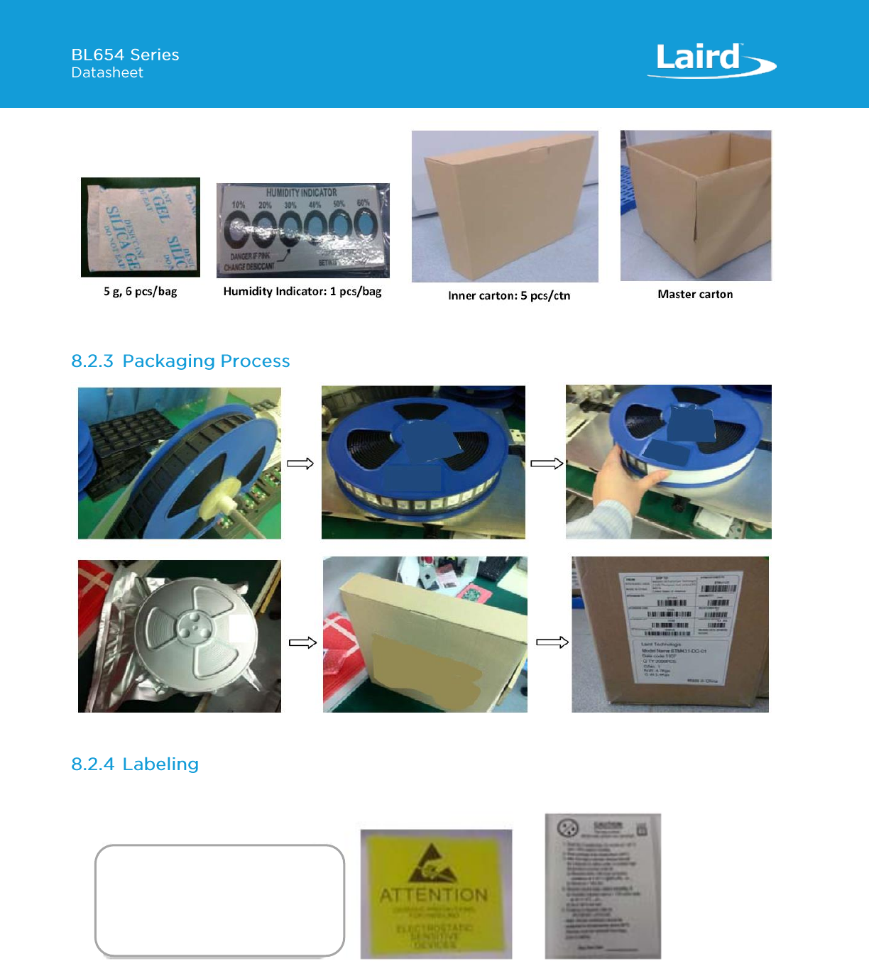
Embedded Wireless Solutions Support Center:
http://ews-support.lairdtech.com
www.lairdtech.com/bluetooth
45
© Copyright 2018 Laird. All Rights Reserved
Americas: +1-800-492-2320
Europe: +44-1628-858-940
Hong Kong: +852 2923 0610
Figure 14: BL654 packaging process
The following labels are located on the antistatic bag:
Figure 15: Antistatic bag labels
Figure 13: Carton contents for the BL654
M/N:451-00001
QTY:1000PCS
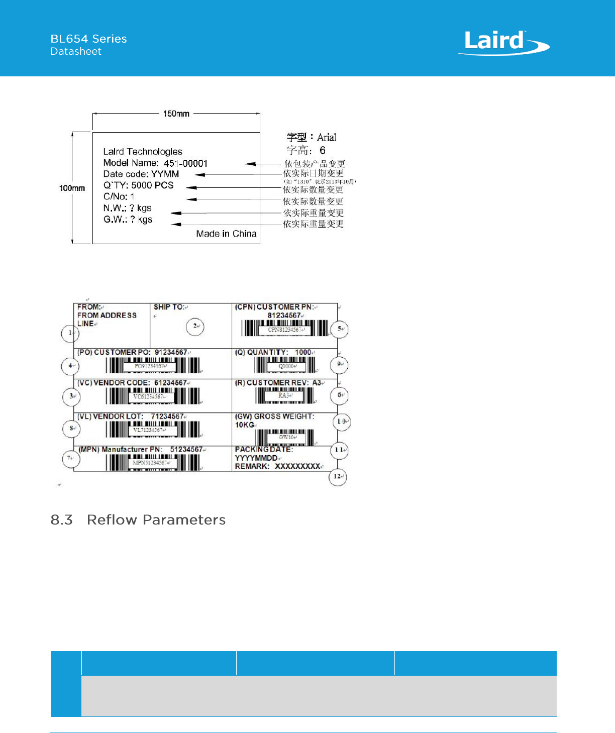
Embedded Wireless Solutions Support Center:
http://ews-support.lairdtech.com
www.lairdtech.com/bluetooth
46
© Copyright 2018 Laird. All Rights Reserved
Americas: +1-800-492-2320
Europe: +44-1628-858-940
Hong Kong: +852 2923 0610
The following package label is located on both sides of the master carton:
Figure 16: Master carton package label
The following is the packing slip label:
Figure 17: Packing slip label
Prior to any reflow, it is important to ensure the modules were packaged to prevent moisture absorption. New packages
contain desiccate (to absorb moisture) and a humidity indicator card to display the level maintained during storage and
shipment. If directed to bake units on the card, see Table 26 and follow instructions specified by IPC/JEDEC J-STD-033. A copy
of this standard is available from the JEDEC website: http://www.jedec.org/sites/default/files/docs/jstd033b01.pdf
Any modules not manufactured before exceeding their floor life should be re-packaged with fresh desiccate and a new
humidity indicator card. Floor life for MSL (Moisture Sensitivity Level) 4 devices is 168 hours in ambient environment
30°C/60%RH.
Table 26: Recommended baking times and temperatures
MSL
125°C
Baking Temp.
90°C/≤ 5%RH
Baking Temp.
40°C/ ≤ 5%RH
Baking Temp.
Saturated
@
30°C/85%
Floor Life Limit
+ 72 hours
@ 30°C/60%
Saturated
@
30°C/85%
Floor Life Limit
+ 72 hours
@ 30°C/60%
Saturated
@ 30°C/85%
Floor Life Limit
+ 72 hours @
30°C/60%
3
9 hours
7 hours
33 hours
23 hours
13 days
9 days
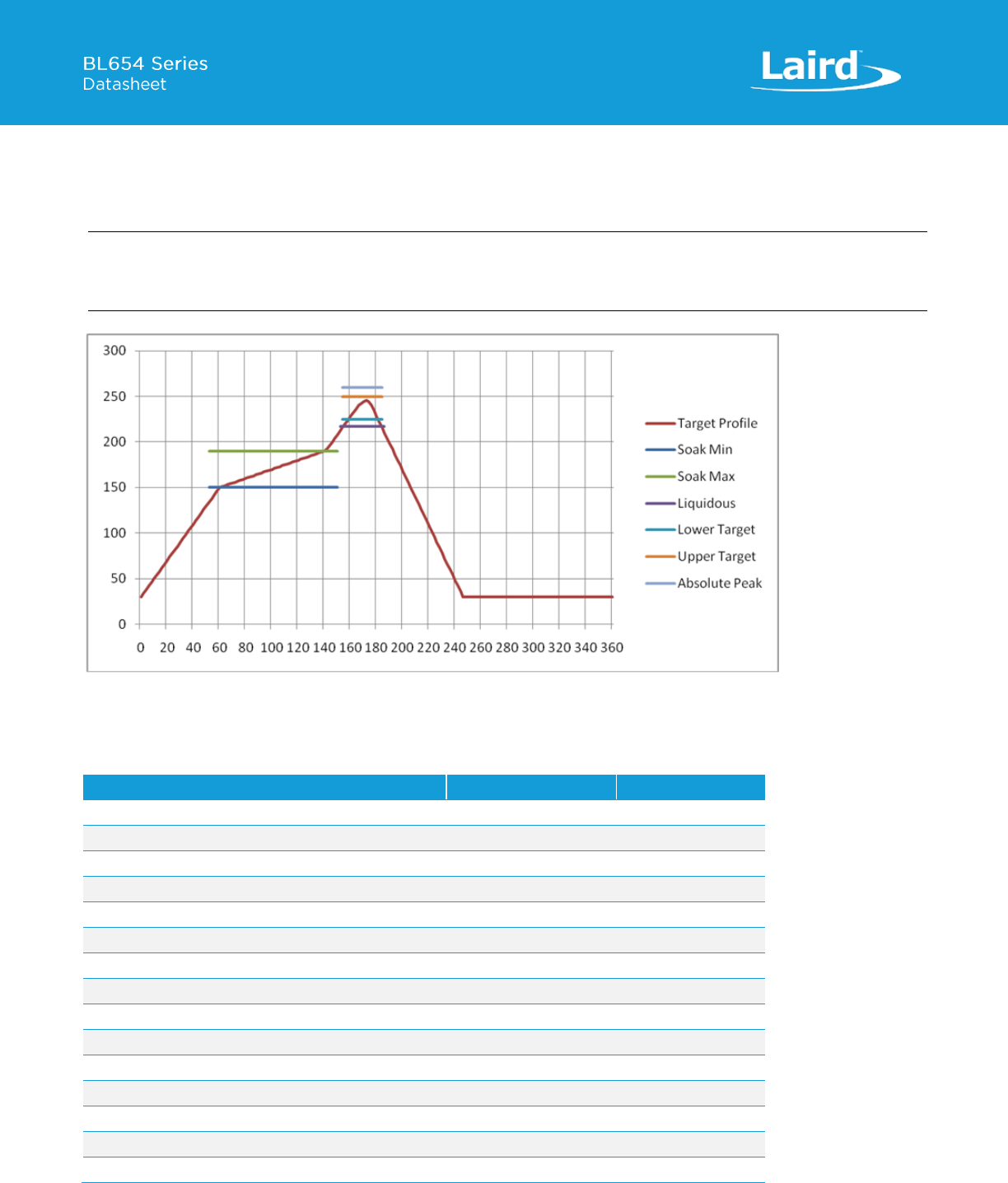
Embedded Wireless Solutions Support Center:
http://ews-support.lairdtech.com
www.lairdtech.com/bluetooth
47
© Copyright 2018 Laird. All Rights Reserved
Americas: +1-800-492-2320
Europe: +44-1628-858-940
Hong Kong: +852 2923 0610
Laird surface mount modules are designed to be easily manufactured, including reflow soldering to a PCB. Ultimately it is the
responsibility of the customer to choose the appropriate solder paste and to ensure oven temperatures during reflow meet
the requirements of the solder paste. Laird surface mount modules conform to J-STD-020D1 standards for reflow
temperatures.
Important: During reflow, modules should not be above 260° and not for more than 30 seconds. In addition, we
recommend that the BL654 module does not go through the reflow process more than one time, otherwise
the BL654 internal component soldering may be impacted.
Figure 18: Recommended reflow temperature
Temperatures should not exceed the minimums or maximums presented in Table 27.
Table 27: Recommended maximum and minimum temperatures
Specification
Value
Unit
Temperature Inc./Dec. Rate (max)
1~3
°C / Sec
Temperature Decrease rate (goal)
2-4
°C / Sec
Soak Temp Increase rate (goal)
.5 - 1
°C / Sec
Flux Soak Period (Min)
70
Sec
Flux Soak Period (Max)
120
Sec
Flux Soak Temp (Min)
150
°C
Flux Soak Temp (max)
190
°C
Time Above Liquidous (max)
70
Sec
Time Above Liquidous (min)
50
Sec
Time In Target Reflow Range (goal)
30
Sec
Time At Absolute Peak (max)
5
Sec
Liquidous Temperature (SAC305)
218
°C
Lower Target Reflow Temperature
240
°C
Upper Target Reflow Temperature
250
°C
Absolute Peak Temperature
260
°C
Embedded Wireless Solutions Support Center:
http://ews-support.lairdtech.com
www.lairdtech.com/bluetooth
48
© Copyright 2018 Laird. All Rights Reserved
Americas: +1-800-492-2320
Europe: +44-1628-858-940
Hong Kong: +852 2923 0610
Model
US/FCC
Canada/IC
451-00001
Pending
Pending
451-00002
Pending
Pending
The 451-00001 and the 451-00002 hold full modular approvals. The OEM must follow the regulatory guidelines and warnings
listed below to inherit the modular approval.
Part #
Form Factor
Tx Outputs
Antenna
451-00001
Surface Mount
8 dBm
PCB Trace
451-00002
Surface Mount
8 dBm
IPEX MHF4
The BL654 family has been designed to operate with the antennas listed below with a maximum gain of 2 dBi. The required
antenna impedance is 50 ohms.
Manufacturer
Model
Laird
Part Number
Type
Connector
Peak Gain
2400-2500 MHz
2400-2480 MHz
Laird
NanoBlue
TBD
PCB Dipole
IPEX MHF4
2 dBi
-
Laird
FlexPIFA
001-0022
PCB Dipole
IPEX MHF4
-
2 dBi
Laird
FlexNotch
001-0023
PCB Dipole
IPEX MHF4
-
2 dBI
Mag.Layers
EDA-8709-2G4C1-B27-CY
0600-00057
Dipole
IPEX MHF4
2 dBi
-
Laird
mFlexPIFA
EFA2400A3S-10MH4L
PIFA
IPEX MHF4
-
2 dBI
Laird
Laird NFC
0600-00061
NFC
N/A
-
-
Laird
BL654-SA PCB printed antenna
NA
Printed PCB
N/A
0 dBi
-
Walsin
RFDPA870900SBAB8G1
NA
Dipole
SMA
2dBi
Note: The OEM is free to choose another vendor’s antenna of like type and equal or lesser gain as an antenna appearing
in the table and still maintain compliance. Reference FCC Part 15.204(c)(4) for further information on this topic.
To reduce potential radio interference to other users, the antenna type and gain should be chosen so that the
equivalent isotropic radiated power (EIRP) is not more than that permitted for successful communication.
This EUT is in compliance with SAR for general population/uncontrolled exposure limits in ANSI/IEEE C95.1-1999 and had
been tested in accordance with the measurement methods and procedures specified in OET Bulletin 65 Supplement C.
This transceiver must not be co-located or operating in conjunction with any other antenna, transmitter, or external
amplifiers. Further testing/evaluation of the end product will be required if the OEM’s device violates any of these
requirements.
The BL654 is fully approved for mobile and portable applications.
Embedded Wireless Solutions Support Center:
http://ews-support.lairdtech.com
www.lairdtech.com/bluetooth
49
© Copyright 2018 Laird. All Rights Reserved
Americas: +1-800-492-2320
Europe: +44-1628-858-940
Hong Kong: +852 2923 0610
WARNING: The OEM must ensure that FCC labelling requirements are met. This includes a clearly visible label on the
outside of the OEM enclosure specifying the appropriate Laird Technology FCC identifier for this product.
Contains FCC ID: XXXXX (Pending)
If the size of the end product is larger than 8x10cm, then the following FCC part 15.19 statement must also
be available on visible on outside of device:
The enclosed device complies with Part 15 of the FCC Rules. Operation is subject to the following two
conditions: (1) This device may not cause harmful interference, and (2) This device must accept any
interference received, including interference that may cause undesired operation
Label and text information should be in a size of type large enough to be readily legible, consistent with the dimensions of the
equipment and the label. However, the type size for the text is not required to be larger than eight points.
CAUTION: The OEM should have their device which incorporates the BL654 tested by a qualified test house to verify
compliance with FCC Part 15 Subpart B limits for unintentional radiators.
CAUTION: Any changes or modifications not expressly approved by Laird Technology could void the user’s authority to
operate the equipment.
This equipment has been tested and found to comply with the limits for a Class B digital device, pursuant to Part 15 of the
FCC Rules. These limits are designed to provide reasonable protection against harmful interference in a residential
installation. This equipment generates, uses and can radiate radio frequency energy and, if not installed and used in
accordance with the instructions, may cause harmful interference to radio communications. However, there is no guarantee
that interference will not occur in a particular installation. If this equipment does cause harmful interference to radio or
television reception, which can be determined by turning the equipment off and on, the user is encouraged to try to correct
the interference by one of the following measures:
▪ Reorient or relocate the receiving antenna.
▪ Increase the separation between the equipment and receiver.
▪ Connect the equipment into an outlet on a circuit different from that to which the receiver is connected.
▪ Consult the dealer or an experienced radio/TV technician for help.
FCC Caution: Any changes or modifications not expressly approved by the party responsible for compliance could void the
user's authority to operate this equipment.
This device complies with Part 15 of the FCC Rules. Operation is subject to the following two conditions: (1) This device may
not cause harmful interference, and (2) this device must accept any interference received, including interference that may
cause undesired operation.
IMPORTANT NOTE:
FCC Radiation Exposure Statement:
This product complies with the US portable RF exposure limit set forth for an uncontrolled environment and are safe for
intended operation as described in this manual. The further RF exposure reduction can be achieved if the product can be
kept as far as possible from the user body or set the device to lower output power if such function is available.
Country Code selection feature to be disabled for products marketed to the US/CANADA.

Embedded Wireless Solutions Support Center:
http://ews-support.lairdtech.com
www.lairdtech.com/bluetooth
50
© Copyright 2018 Laird. All Rights Reserved
Americas: +1-800-492-2320
Europe: +44-1628-858-940
Hong Kong: +852 2923 0610
This device is intended only for OEM integrators under the following conditions:
1. The transmitter module may not be co-located with any other transmitter or antenna,
As the condition above is met, further transmitter testing is not required. However, the OEM integrator is still responsible for
testing their end-product for any additional compliance requirements required with this module installed.
IMPORTANT NOTE
If these conditions cannot be met (for example certain laptop configurations or co-location with another transmitter), then
the FCC authorization is no longer considered valid and the FCC ID cannot be used on the final product. In these
circumstances, the OEM integrator is responsible for re-evaluating the end product (including the transmitter) and obtaining
a separate FCC authorization.
End Product Labeling
The final end product must be labeled in a visible area with the following: Contains FCC ID: SQGBL654.
Manual Information to the End User
The OEM integrator must be aware not to provide information to the end user regarding how to install or remove this RF
module in the user’s manual of the end product which integrates this module.
The end user manual shall include all required regulatory information/warning as show in this manual.
This device contains licence-exempt transmitter(s)/receiver(s) that comply with Innovation, Science and Economic
Development Canada’s licence-exempt RSS(s). Operation is subject to the following two conditions:
(1) This device may not cause interference
(2) This device must accept any interference, including interference that may cause undesired operation of the device.
Cet Cet appareil contient des émetteurs / récepteurs exempts de licence qui sont conformes au (x) RSS (s) exemptés de
licence d'Innovation, Sciences et Développement économique Canada. L'opération est soumise aux deux conditions
suivantes:
(1) Cet appareil ne doit pas causer d'interférences
(2) Cet appareil doit accepter toute interférence, y compris les interférences pouvant provoquer un fonctionnement
indésirable de l'appareil
This radio transmitter (IC: 3147A-BL654) has been approved by Industry Canada to operate with the antenna types listed
below with the maximum permissible gain indicated. Antenna types not included in this list, having a gain greater than the
maximum gain indicated for that type, are strictly prohibited for use with this device.
Le présent émetteur radio (IC: 3147A-BL654) a été approuvé par Industrie Canada pour fonctionner avec les types d'antenne
énumérés ci dessous et ayant un gain admissible maximal. Les types d'antenne non inclus dans cette liste, et dont le gain est
supérieur au gain maximal indiqué, sont strictement interdits pour l'exploitation de l'émetteur.
Manufacturer
Model
Type
2400-2500 MHz
2400-2480 MHz
Laird
NanoBlue
PCB Dipole
2dBi
Laird
FlexPIFA
PCB Dipole
2dBi
Laird
FlexNotch
PCB Dipole
2dBI
Mag.Layers
EDA-8709-2G4C1-B27-CY
Dipole
2dBi
Laird
mFlexPIFA
PIFA
2dBI
Embedded Wireless Solutions Support Center:
http://ews-support.lairdtech.com
www.lairdtech.com/bluetooth
51
© Copyright 2018 Laird. All Rights Reserved
Americas: +1-800-492-2320
Europe: +44-1628-858-940
Hong Kong: +852 2923 0610
Manufacturer
Model
Type
2400-2500 MHz
2400-2480 MHz
Laird
Laird NFC
NFC
Laird
BL654-SA PCB printed antenna
Printed PCB
0dBi
Walsin
RFDPA870900SBAB8G1
Dipole
2dBi
Radiation Exposure Statement:
This equipment complies with Canada radiation exposure limits set forth for an uncontrolled environment. This equipment
should be installed and operated with minimum distance 20cm between the radiator and your body.
Déclaration d'exposition aux radiations:
Cet équipement est conforme Canada limites d'exposition aux radiations dans un environnement non contrôlé. Cet
équipement doit être installé et utilisé à distance minimum de 20cm entre le radiateur et votre corps.
This device is intended only for OEM integrators under the following conditions:
1. The transmitter module may not be co-located with any other transmitter or antenna.
If the condition above is met, further transmitter testing is not required. However, the OEM integrator is still responsible for
testing their end-product for any additional compliance requirements required with this module installed.
Cet appareil est conçu uniquement pour les intégrateurs OEM dans les conditions suivantes:
1. Le module émetteur peut ne pas être coïmplanté avec un autre émetteur ou antenne.
Tant que les 1 condition ci-dessus sont remplies, des essais supplémentaires sur l'émetteur ne seront pas nécessaires.
Toutefois, l'intégrateur OEM est toujours responsable des essais sur son produit final pour toutes exigences de conformité
supplémentaires requis pour ce module installé.
IMPORTANT NOTE:
If these conditions cannot be met (for example certain laptop configurations or co-location with another transmitter), then
the Canada authorization is no longer considered valid and the IC ID cannot be used on the final product. In these
circumstances, the OEM integrator will be responsible for re-evaluating the end product (including the transmitter) and
obtaining a separate Canada authorization.
NOTE IMPORTANTE:
Dans le cas où ces conditions ne peuvent être satisfaites (par exemple pour certaines configurations d'ordinateur portable ou
de certaines co-localisation avec un autre émetteur), l'autorisation du Canada n'est plus considéré comme valide et l'ID IC ne
peut pas être utilisé sur le produit final. Dans ces circonstances, l'intégrateur OEM sera chargé de réévaluer le produit final (y
compris l'émetteur) et l'obtention d'une autorisation distincte au Canada.
End Product Labeling
The final end product must be labeled in a visible area with the following: Contains IC: 3147A-BL654.
Plaque signalétique du produit final
Le produit final doit être étiqueté dans un endroit visible avec l'inscription suivante: Contains IC: 3147A-BL654.
Manual Information to the End User
The OEM integrator must be aware not to provide information to the end user regarding how to install or remove this RF
module in the user’s manual of the end product which integrates this module.
The end user manual shall include all required regulatory information/warning as show in this manual.
Embedded Wireless Solutions Support Center:
http://ews-support.lairdtech.com
www.lairdtech.com/bluetooth
52
© Copyright 2018 Laird. All Rights Reserved
Americas: +1-800-492-2320
Europe: +44-1628-858-940
Hong Kong: +852 2923 0610
Manuel d'information à l'utilisateur final
L'intégrateur OEM doit être conscient de ne pas fournir des informations à l'utilisateur final quant à la façon d'installer ou de
supprimer ce module RF dans le manuel de l'utilisateur du produit final qui intègre ce module.
Le manuel de l'utilisateur final doit inclure toutes les informations réglementaires requises et avertissements comme indiqué
dans ce manuel.
The BL654 is approved for use in the Japanese market. The part numbers listed below hold WW type certification. Refer to
ARIB-STD-T66 for further guidance on OEM’s responsibilities.
Model
Certificate Number
Antenna
451-00001
Pending
PCB Trace
451-00002
Pending
IPEX MHF4
The BL654 was tested with antennas listed below. The OEM can choose a different manufacturers antenna but must make
sure it is of same type and that the gain is lesser than or equal to the antenna that is approved for use.
Manufacturer
Model
Laird
Part Number
Type
Connector
Peak Gain
2400-2500 MHz
2400-2480 MHz
Laird
NanoBlue
TBD
PCB Dipole
IPEX MHF4
2 dBi
-
Laird
FlexPIFA
001-0022
PCB Dipole
IPEX MHF4
-
2 dBi
Laird
FlexNotch
001-0023
PCB Dipole
IPEX MHF4
-
2 dBI
Mag.Layers
EDA-8709-2G4C1-B27-CY
0600-00057
Dipole
IPEX MHF4
2 dBi
-
Laird
mFlexPIFA
EFA2400A3S-10MH4L
PIFA
IPEX MHF4
-
2 dBI
Laird
Laird NFC
0600-00061
NFC
N/A
-
-
Laird
BL654-SA PCB printed antenna
NA
Printed PCB
N/A
0 dBi
-
Walsin
RFDPA870900SBAB8G1
NA
Dipole
SMA
2dBi
Embedded Wireless Solutions Support Center:
http://ews-support.lairdtech.com
www.lairdtech.com/bluetooth
53
© Copyright 2018 Laird. All Rights Reserved
Americas: +1-800-492-2320
Europe: +44-1628-858-940
Hong Kong: +852 2923 0610
.
The 451-00001/451-00002 have been tested for compliance with relevant standards for the EU market. The 451-00002
module was tested with a 2.21 dBi antenna. The OEM can operate the 451-00002 module with any other type of antenna but
must ensure that the gain does not exceed 2.21 dBi to maintain the Laird approval.
The OEM should consult with a qualified test house before entering their device into an EU member country to make sure all
regulatory requirements have been met for their complete device.
Reference the Declaration of Conformities listed below for a full list of the standards that the modules were tested to. Test
reports are available upon request.
The antennas listed below were tested for use with the BL654. For CE mark countries, the OEM is free to use any
manufacturer’s antenna and type of antenna if the gain is less than or equal to the highest gain approved for use (2.21dBi)
Contact a Laird representative for more information regarding adding antennas.
Manufacturer
Model
Laird
Part Number
Type
Connector
Peak Gain
2400-2500 MHz
2400-2480 MHz
Laird
NanoBlue
TBD
PCB Dipole
IPEX MHF4
2 dBi
-
Laird
FlexPIFA
001-0022
PCB Dipole
IPEX MHF4
-
2 dBi
Laird
FlexNotch
001-0023
PCB Dipole
IPEX MHF4
-
2 dBI
Mag.Layers
EDA-8709-2G4C1-B27-CY
0600-00057
Dipole
IPEX MHF4
2 dBi
-
Laird
mFlexPIFA
EFA2400A3S-10MH4L
PIFA
IPEX MHF4
-
2 dBI
Laird
Laird NFC
0600-00061
NFC
N/A
-
-
Laird
BL654-SA PCB printed antenna
NA
Printed PCB
N/A
0 dBi
-
Walsin
RFDPA870900SBAB8G1
NA
Dipole
SMA
2dBi
Note: The BL654 module internal BLE chipset IC pins are rated 4 kV (ESD HBM). ESD can find its way through the external
JTAG connector (if used on the customer’s design), if discharge is applied directly. Customer should ensure
adequate protection against ESD on their end product design (using the BL654 module) to meet relevant ESD
standard (for CE, this is EN301-489).
This device complies with the essential requirements of the Radio Equipment directive: 2014/53/EU. The following test
methods have been applied to prove presumption of conformity with the essential requirements of the Radio Equipment
directive: 2014/53/EU:
▪ EN 300 328 V2.1.1
▪ EN 300 330 V2.1.1
▪ EN 301 489-1 V2.2.0 (Draft)
▪ EN 301 489-3 V2.1.1 (Draft)
▪ EN 301 489-17 V3.2.0(Draft)
▪ EN 50385:2017
▪ EN 62311:2008
▪ EN 60950-1: 2006+A11:2009+A1:2010+A12:2011+A2:2013
2400~2480MHz, 9.5 dBm, SW version: 29.1.1.0
The minimum distance between the user and/or any bystander and the radiating structure of the transmitter is 20cm.
Embedded Wireless Solutions Support Center:
http://ews-support.lairdtech.com
www.lairdtech.com/bluetooth
54
© Copyright 2018 Laird. All Rights Reserved
Americas: +1-800-492-2320
Europe: +44-1628-858-940
Hong Kong: +852 2923 0610
Part Number
Product Description
451-00001
Bluetooth v5/802.15.4/NFC module – Integrated antenna
451-00002
Bluetooth v5 / 802.15.4 / NFC module – External antenna
451-00003
Intelligent USB Bluetooth v5 adapter
455-00001
Development Kit for 451-00001 module – Integrated antenna
455-00002
Development Kit for the 451-00002 module – External antenna
The BL654 module is listed on the Bluetooth SIG website as a qualified End Product.
Design
Name
Owner
Declaration ID
QD ID
Link to listing on the SIG website
BL654
Laird
Technologies
BL654*
Laird
Technologies
It is a mandatory requirement of the Bluetooth Special Interest Group (SIG) that every product implementing Bluetooth
technology has a Declaration ID. Every Bluetooth design is required to go through the qualification process, even when
referencing a Bluetooth Design that already has its own Declaration ID. The Qualification Process requires each company to
registered as a member of the Bluetooth SIG – www.bluetooth.org
The following link provides a link to the Bluetooth Registration page: https://www.bluetooth.org/login/register/
For each Bluetooth Design, it is necessary to purchase a Declaration ID. This can be done before starting the new
qualification, either through invoicing or credit card payment. The fees for the Declaration ID will depend on your
membership status, please refer to the following webpage:
https://www.bluetooth.org/en-us/test-qualification/qualification-overview/fees
For a detailed procedure of how to obtain a new Declaration ID for your design, please refer to the following SIG document:
https://www.bluetooth.org/DocMan/handlers/DownloadDoc.ashx?doc_id=283698&vId=317486
To start a listing, go to: https://www.bluetooth.org/tpg/QLI_SDoc.cfm
In step 1, select the option, Reference a Qualified Design and enter XXXXX in the End Product table entry. You can then select
your pre-paid Declaration ID from the drop-down menu or go to the Purchase Declaration ID page, (please note that unless
the Declaration ID is pre-paid or purchased with a credit card, it will not be possible to proceed until the SIG invoice is paid.
Once all the relevant sections of step 1 are finished, complete steps 2, 3, and 4 as described in the help document. Your new
Design will be listed on the SIG website and you can print your Certificate and Declaration of Conformity.
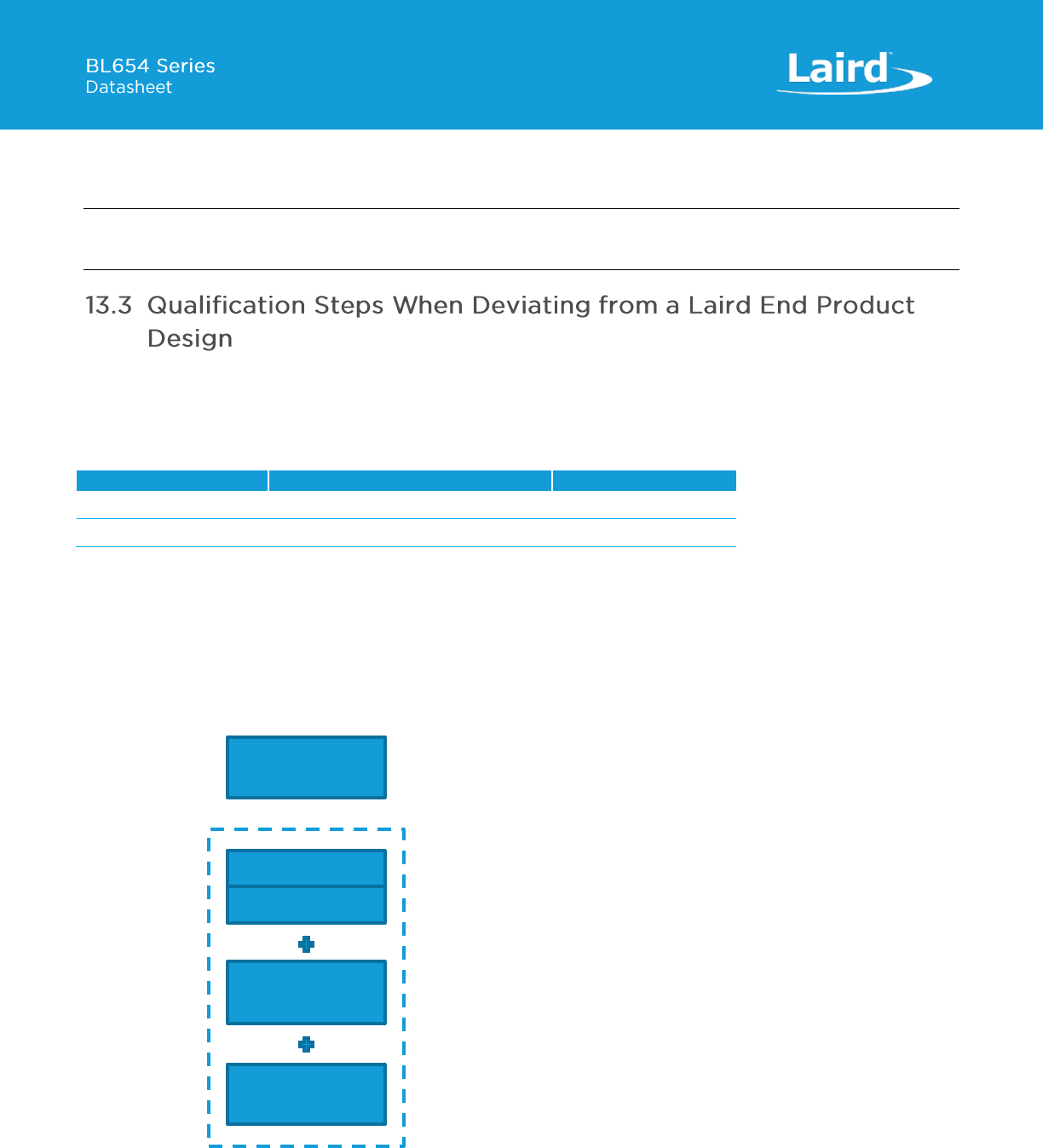
Embedded Wireless Solutions Support Center:
http://ews-support.lairdtech.com
www.lairdtech.com/bluetooth
55
© Copyright 2018 Laird. All Rights Reserved
Americas: +1-800-492-2320
Europe: +44-1628-858-940
Hong Kong: +852 2923 0610
For further information, please refer to the following training material:
https://www.bluetooth.org/en-us/test-qualification/qualification-overview/listing-process-updates
Note: If using the BL654 with Laird Firmware and smartBASIC script, you can skip “Controller Subsystem”, “Host
Subsystem”, and “Profile Subsystem”.
If you wish to deviate from the standard End Product design listed under XXXXX, the qualification process follows the
Traditional Project route, creating a new design. When creating a new design, it is necessary to complete the full qualification
listing process and also maintain a compliance folder for the new design.
The BL654 design under XXXXX incorporates the following components:
Listing reference
Design Name
Core Spec Version
In the future, Nordic may list updated versions of these components and it is possible to use them in your new design. Please
check with Nordic to make sure these software components are compatible with the nRF52 hardware XXXXX
If your design is based on un-modified BL654 hardware it is possible use the following process;
2. Reference the existing RF-PHY test report from the BL654 listing.
3. Combine the relevant Nordic Link Layer (LL) – check QDID with Nordic.
4. Combine in a Host Component (covering L2CAP, GAP, ATT, GATT, SM) - check QDID with Nordic.
5. Test any standard SIG profiles that are supported in the design (customs profiles are exempt).
Figure 19: Scope of the qualification for an End Product Design
The first step is to generate a project on the TPG (Test Plan Generator) system. This determines which test cases apply to
demonstrate compliance with the Bluetooth Test Specifications. If you are combining pre-tested and qualified components in
End
Product
Laird RF-PHY
Nordic LL
Host
Layers
Profiles
Embedded Wireless Solutions Support Center:
http://ews-support.lairdtech.com
www.lairdtech.com/bluetooth
56
© Copyright 2018 Laird. All Rights Reserved
Americas: +1-800-492-2320
Europe: +44-1628-858-940
Hong Kong: +852 2923 0610
your design and they are within their three-year listing period, you are not required to re-test those layers covered by these
components.
If the design incorporates any standard SIG LE profiles (such as Heart Rate Profile), it is necessary to test these profiles using
PTS or other tools where permitted; the results are added to the compliance folder.
You are required to upload your test declaration and test reports (where applicable) and then complete the final listing steps
on the SIG website. Remember to purchase your Declaration ID before you start the qualification process, as it’s impossible to
complete the listing without it.
Please contact your local sales representative or our support team for further assistance:
Laird Technologies Connectivity Products Business Unit
Support Centre: http://ews-support.lairdtech.com
Email: wireless.support@lairdtech.com
Phone: Americas: +1-800-492-2320
Europe: +44-1628-858-940
Hong Kong: +852 2923 0610
Web: http://www.lairdtech.com/bluetooth
Note: This is a PRELIMINARY version of the BL654 datasheet.
Information contained in this document is subject to change.
© Copyright 2018 Laird. All Rights Reserved. Patent pending. Any information furnished by Laird and its agents is believed to be accurate and reliable. All
specifications are subject to change without notice. Responsibility for the use and application of Laird materials or products rests with the end user since
Laird and its agents cannot be aware of all potential uses. Laird makes no warranties as to non-infringement nor as to the fitness, merchantability, or
sustainability of any Laird materials or products for any specific or general uses. Laird, Laird Technologies, Inc., or any of its affiliates or agents shall not be
liable for incidental or consequential damages of any kind. All Laird products are sold pursuant to the Laird Terms and Conditions of Sale in effect from time
to time, a copy of which will be furnished upon request. When used as a tradename herein, Laird means Laird PLC or one or more subsidiaries of Laird PLC.
Laird™, Laird Technologies™, corresponding logos, and other marks are trademarks or registered trademarks of Laird. Other marks may be the property of
third parties. Nothing herein provides a license under any Laird or any third party intellectual property right.