Laird Connectivity BT830 Bluetooth v4.0 Dual-Mode UART HCI Module User Manual
Laird Technologies Bluetooth v4.0 Dual-Mode UART HCI Module
User manual

Bluetooth v4.0 Dual-Mode UART HCI Module
BT830 – Hardware Integration Guide (HIG)
Version 0.1 - PRELIMINARY
Americas: +1-800-492-2320 Option 2
Europe: +44-1628-858-940
Hong Kong: +852-2923-0610
www.lairdtech.com/bluetooth

BT830 Hardware Integration Guide
Version 0.1 (PRELIMINARY)
Americas: +1-800-492-2320 Option 2
Europe: +44-1628-858-940
Hong Kong: +852-2923-0610
www.lairdtech.com/bluetooth
2
CONN-GUIDE-BT830
(PRELIMINARY)
REVISION HISTORY
Revision
Date
Changes
0.1
26 March 2014
Initial preliminary version

BT830 Hardware Integration Guide
Version 0.1 (PRELIMINARY)
Americas: +1-800-492-2320 Option 2
Europe: +44-1628-858-940
Hong Kong: +852-2923-0610
www.lairdtech.com/bluetooth
3
CONN-GUIDE-BT830
(PRELIMINARY)
CONTENTS
Revision History............................................................................................................................................. 2
Contents ...................................................................................................................................................... 3
1 Scope ..................................................................................................................................................... 4
2 Operational Description .......................................................................................................................... 4
2.1 Features & Benefits ......................................................................................................................... 4
2.2 Application Areas ........................................................................................................................... 4
3 Block Diagram and Descriptions .............................................................................................................. 5
4 Specifications ......................................................................................................................................... 6
5 Pin Definitions ........................................................................................................................................ 7
6 DC Electrical Characteristic ..................................................................................................................... 9
7 RF Characteristics ................................................................................................................................. 10
8 Interface ............................................................................................................................................... 11
8.1 PIO ............................................................................................................................................... 11
8.2 WLAN Coexistence Interface ......................................................................................................... 11
8.3 UART Interface ............................................................................................................................. 12
8.4 PCM Interface .............................................................................................................................. 12
8.5 GCI Interface ................................................................................................................................ 15
8.6 Slots and Sample Formats ............................................................................................................. 15
8.7
PCM Timing Information
............................................................................................................... 16
8.8 PCM Slave Timing ........................................................................................................................ 18
8.9 PCM Slave Mode Timing Parameters ............................................................................................. 18
8.10 PCM_CLK and PCM_SYNC Generation ......................................................................................... 20
8.11 PCM Configuration ...................................................................................................................... 20
8.12 Digital Audio Interface (I²S) ........................................................................................................... 20
9 Power Supply and Regulation ............................................................................................................... 23
9.1 Voltage Regulator Enable and Reset ............................................................................................. 23
9.2 Power Sequencing ........................................................................................................................ 24
10 Antenna Performance........................................................................................................................... 24
11 Mechanical Dimensions and Land Pattern ............................................................................................. 26
11.1 BT830 Mechanical Drawing .......................................................................................................... 26
12 Implementation Note............................................................................................................................ 27
12.1 PCB Layout on Host PCB............................................................................................................... 27
13 Application Note for Surface Mount Modules ....................................................................................... 28
13.1 Introduction ................................................................................................................................. 28
13.2 Shipping tray ................................................................................................................................ 28
13.3 Reflow Parameters ....................................................................................................................... 29
14 FCC and IC Regulatory ......................................................................................................................... 30
14.1 Documentation Requirements ...................................................................................................... 30
15 European Union Regulatory .................................................................................................................. 32
15.1 EU Declarations of Conformity ...................................................................................................... 33
16 Ordering Information............................................................................................................................ 33
16.1 General Comments ...................................................................................................................... 33
17 Bluetooth SIG Approvals ....................................................................................................................... 34
17.1 Application Note: Subsystem Combinations .................................................................................. 34
17.2 Additional Assistance ................................................................................................................... 35
BT830 Hardware Integration Guide
Version 0.1 (PRELIMINARY)
Americas: +1-800-492-2320 Option 2
Europe: +44-1628-858-940
Hong Kong: +852-2923-0610
www.lairdtech.com/bluetooth
4
CONN-GUIDE-BT830
(PRELIMINARY)
1 SCOPE
This document describes key hardware aspects of the Laird BT830 Bluetooth HCI module. This document is intended
to assist device manufacturers and related parties with the integration of this module into their host devices. Data in
this document are drawn from a number of sources including data sheets for the CSR8811.
Because the BT830 is currently in development stage, this document is preliminary and the information in this
document is subject to change. Please contact Laird Technologies or visit the Laird website at www.Lairdtech.com to
obtain the most recent version of this document.
2 OPERATIONAL DESCRIPTION
The BT830 series of UART HCI devices are designed to meet the needs of OEMs adding
robust Bluetooth connectivity and using embedded Bluetooth stacks within these products.
Leveraging the market-leading CSR8811 chipset, the BT830 series provides exceptionally
low power consumption with outstanding range. Supporting the latest Bluetooth v4.0
Specification with EDR (Enhanced Data Rate), the Laird BT830 series enables OEMs to
accelerate their development time for leveraging either Classic Bluetooth or Bluetooth Low
Energy (BLE) into their operating system based devices.
With a tiny footprint as small as 8.5 x 13 mm, yet output power at 7 dBm, these modules are ideal for applications
where designers need high performance in minimal size. For maximum flexibility in systems integration, the modules
are designed to support a UART interface plus GPIO and additionally I2S and PCM audio interfaces.
These modules present an HCI interface and have native support for Windows and Linux Bluetooth software stacks.
All BT830 series devices are fully qualified as Bluetooth Hardware Controller Subsystem products. This also allows
designers to integrate their existing pre-approved Bluetooth Host and Profile subsystem stacks to gain a Bluetooth
END product approval for their products.
The BT830 series is engineered to provide excellent RF performance with integrated antenna and additional band pass
filters. It further reduces regulatory and testing requirements for OEMs and ensures a hassle free development cycle.
A fully featured, low-cost developer’s kit is available for prototyping, debug, and integration testing of the BT830
series modules and further reduces risk and time in development cycles.
2.1 Features & Benefits
2.2 Application Areas
Bluetooth v4.0 - Dual mode (Classic Bluetooth and BLE)
Compact footprint
2-wire and 3-wire Wi-Fi coexistence scheme
High antenna radiation gain and efficiency
Good interference rejection for multi-com system (GSM/WCDMA)
Class 1 output – 7 dBm
UART, GPIO, I2S, and PCM
Industrial Temperature Range
Bluetooth Hardware Controller subsystem
FCC, IC and CE approvals
Medical devices
ePOS terminals
Barcode scanners
Industrial Cable Replacement
M2M Connectivity
Automotive Diagnostic Equipment
Personal Digital Assistants (PDA)
Bluetooth HID device (keyboard, mouse,
and joystick)
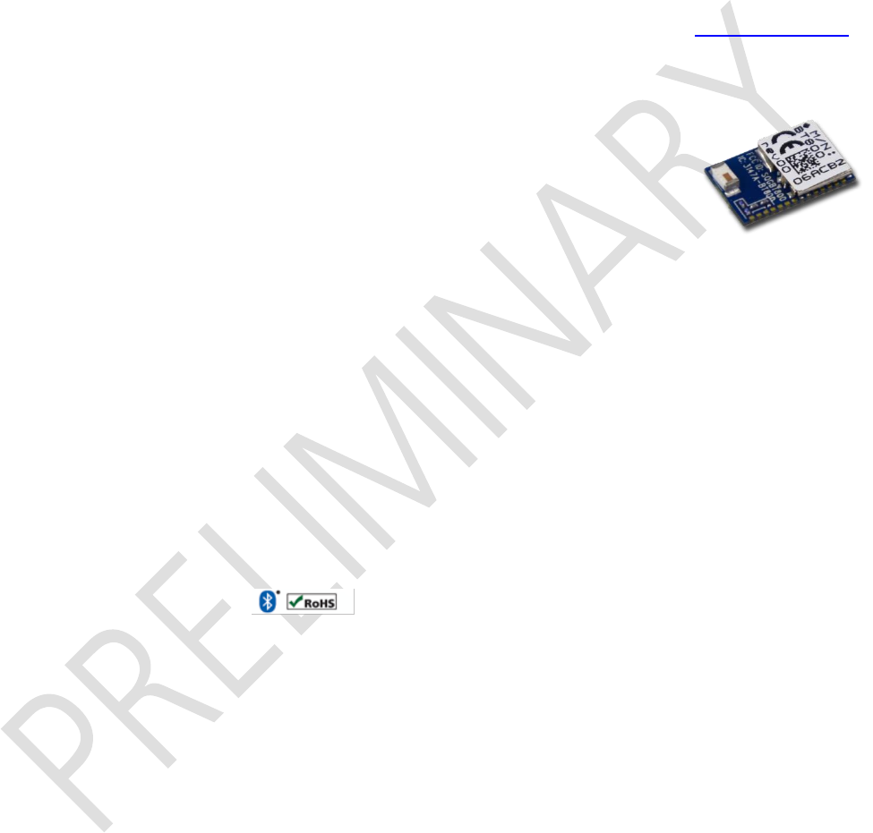
Figure 1: BT830 module
BT830 Hardware Integration Guide
Version 0.1 (PRELIMINARY)
Americas: +1-800-492-2320 Option 2
Europe: +44-1628-858-940
Hong Kong: +852-2923-0610
www.lairdtech.com/bluetooth
5
CONN-GUIDE-BT830
(PRELIMINARY)
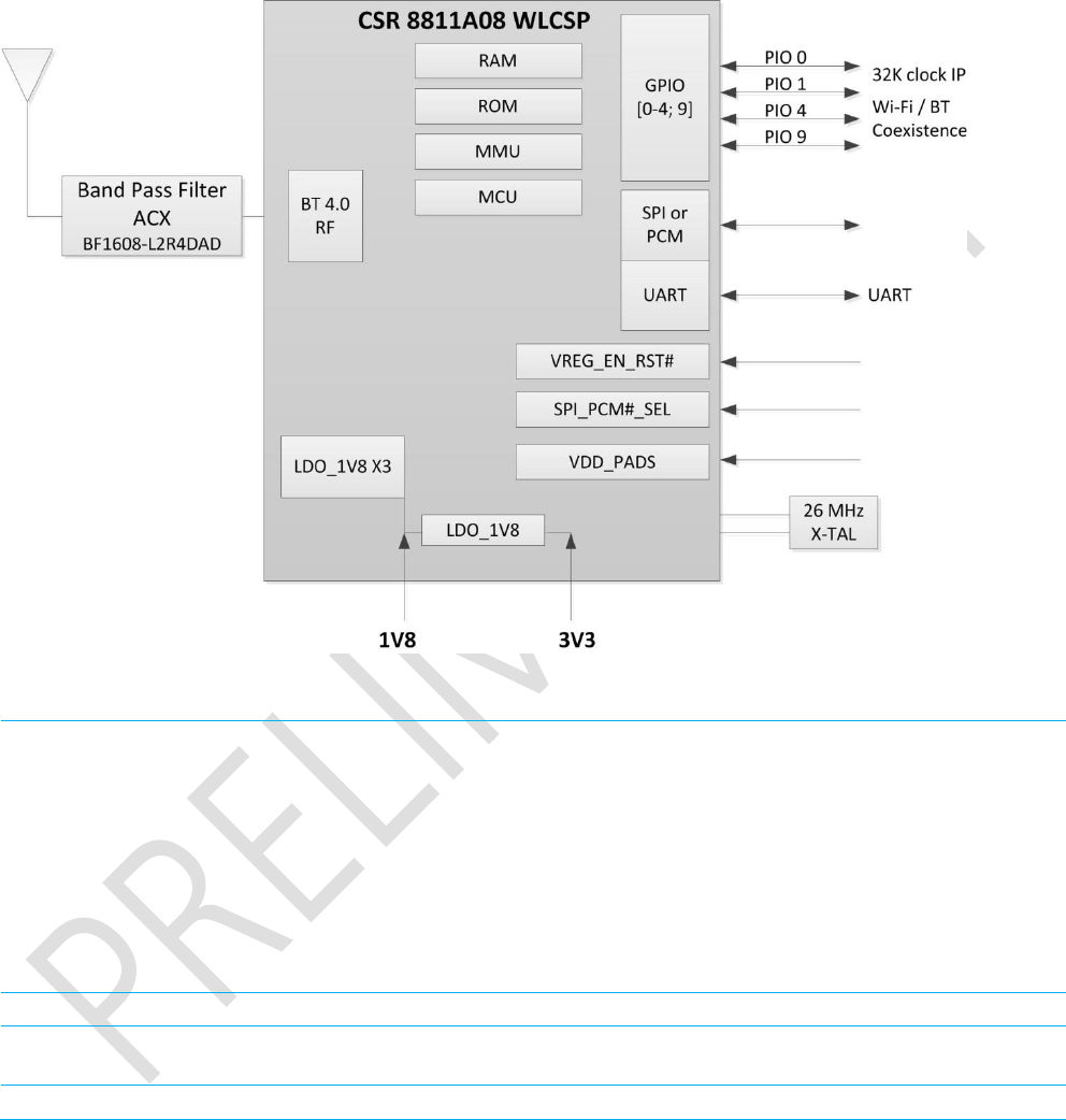
3 BLOCK DIAGRAM AND DESCRIPTIONS
Figure 1: BT830 module block diagram
CS8811A08
(Main chip)
The BT830 is based on CSR8811A08 dual mode chip. The chip is a single-chip radio with on-chip
LDO regulators and baseband IC for Bluetooth 2.4 GHz systems including EDR to 3 Mbps.
Dedicated signal and baseband processing is included for full Bluetooth operation. The chip
provides PCM/I2S and UART interfaces. Up to four general purpose I/Os are available for general
use such as Wi-Fi coexistence or general indicators.
Note: The purpose of the SPI interface is to access the module’s inner settings such as selecting
different WLAN CO-EXIST scheme and enabling HID proxy mode. The SPI interface can
also be used to put the module in RF test mode. You cannot use the module over the SPI
interface for normal operation as the main host interface.
Antenna
The antenna is a ceramic monopole chip antenna.
Band Pass
Filter
The band pass filter filters the out-of-band emissions from the transmitter to meet the specific
regulations for type approvals of various countries.
Crystal
The embedded 26 MHz crystal is used for generating the clock for the entire module.

BT830 Hardware Integration Guide
Version 0.1 (PRELIMINARY)
Americas: +1-800-492-2320 Option 2
Europe: +44-1628-858-940
Hong Kong: +852-2923-0610
www.lairdtech.com/bluetooth
6
CONN-GUIDE-BT830
(PRELIMINARY)
4 SPECIFICATIONS
Table 1: BT830 specifications
CATEGORIES
FEATURE
IMPLEMENTATION
Wireless Specification
Bluetooth®
V4.0 Dual Mode
Frequency
2.402 - 2.480 GHz
Maximum Transmit
Power
Class 1
+7 dBm from antenna
Receive Sensitivity
-89 dBm
Range
Circa 100 meters
Data Rates
Up to 3 Mbps (over the air)
Host Interface
UART
RX, TX, CTS, RTS
GPIO
Four configurable lines
(1.8V/3.3V configurable by VDD_PADS)
Operational Modes
HCI
Host Controller Interface over UART
Coexistence
802.11 (Wi-Fi)
3 wire CSR schemes supported
(Unity-3;Unity-3e, and Unity+)
Supply Voltage
Supply
3.3V +/-10%
Note: See
Implementation Note
for details on different DC
power selections on the BT830.
Power Consumption
Current
Idle Mode ~TBD mA (Master; ACL link; No traffic)
File Transfer ~TBD mA (Master; ACL link; Transmit)
Antenna Option
Internal
Multilayer ceramic antenna with up to 41% efficiency.
Physical
Dimensions
8.5 x 13 x 1.6 mm (BT830 - Module)
Environmental
Operating
-30C to +85C
Storage
-40C to +85C
Miscellaneous
Lead Free
Lead-free and RoHS compliant
Warranty
1 Year
Approvals
Bluetooth®
Hardware Controller Subsystem Approved
FCC / IC / CE
All BT830 series (BT830-SA; BT830-ST)

BT830 Hardware Integration Guide
Version 0.1 (PRELIMINARY)
Americas: +1-800-492-2320 Option 2
Europe: +44-1628-858-940
Hong Kong: +852-2923-0610
www.lairdtech.com/bluetooth
7
CONN-GUIDE-BT830
(PRELIMINARY)
5 PIN DEFINITIONS
Table 2: BT830 pin definitions
#
Pin Name
I/O
Supply Domain
Description
1
VDD_PADS
Power supply
(1.7V-3.6V)
Positive supply for digital I/O pads
2
GND
GND
-
Ground
3
UART_RTS
Bidirectional, tristate,
with weak internal
pullup
VDD_PADS
UART data output, active high
4
UART_TX
Bidirectional, tristate,
with weak internal
pullup
VDD_PADS
UART data input, active high
5
UART_CTS
Bidirectional, tristate,
with weak internal
pullup
VDD_PADS
UART clear to send, active low
6
UART_RX
Bidirectional, tristate,
with weak internal
pullup
VDD_PADS
UART request to send, active low
7
GND
GND
-
Ground
8
VREG_EN_RST#
Input with strong
internal pull-down
VDD_PADS
Take high to enable internal
regulators. Also acts as active low
reset. Maximum voltage is VDD_PADS.
9
VREG_IN_HV
Analogue regulator
input
3.3V
Input to internal high-voltage regulator
10
VREG_OUT_HV
Analogue regulator
input/output
1.8V
Output from internal high-voltage
regulator and input to low-voltage
internal regulators.
11
GND
GND
-
Ground
12
GND
GND
-
Ground
13
GND
GND
-
Ground
14
GND
GND
-
Ground
15
GND
GND
-
Ground
16
GND
GND
-
Ground
17
RF
RF signal out (50 ohm) for BT830-ST
version only.
Not connection for BT830-SA.
18
GND
GND
-
Ground
19
PCM_SYNC/
SPI_CS#/
PIO23
Bidirectional, tri-state,
with weak internal
pull-down
VDD_PADS
PCM synchronous data sync SPI chip
select, active low Programmable
input/output line
*See Note 1.

BT830 Hardware Integration Guide
Version 0.1 (PRELIMINARY)
Americas: +1-800-492-2320 Option 2
Europe: +44-1628-858-940
Hong Kong: +852-2923-0610
www.lairdtech.com/bluetooth
8
CONN-GUIDE-BT830
(PRELIMINARY)
#
Pin Name
I/O
Supply Domain
Description
20
PCM_CLK/ SPI_CLK/
PIO24
Bidirectional, tri-state,
with weak internal
pull-down
VDD_PADS
PCM synchronous data clock
SPI clock
Programmable input/output line
*See Note 1.
21
PCM_IN/ SPI_MOSI/
PIO21
Input, tri-state, with
weak internal pull-
down
VDD_PADS
PCM synchronous data input
SPI data input
Programmable input/output line
*See Note 1.
22
PCM_OUT/
SPI_MISO/
PIO22
Output, tri-state, with
weak internal pull-
down
VDD_PADS
PCM synchronous data output
SPI data output
Programmable input/output line
*See Note 1.
23
GND
GND
-
Ground
24
PIO0/
32K_CLK_IN
Bidirectional, tri-state,
with weak internal pull-
down
VDD_PADS
Programmable input/output line and
32kHz sleep clock input
25
PIO1/
BT_ACTIVE
Bidirectional, tri-state,
with weak internal pull-
down
VDD_PADS
Programmable input/output line;
Wi-Fi & BT 3-wire coexistance
26
PIO9/
BT_PRIORITY
Bidirectional, tri-state,
with weak internal pull-
down
VDD_PADS
Programmable input/output line;
Wi-Fi & BT 3-wire coexistance
27
PIO4/
WLAN_ACTIVE
Bidirectional, tri-state,
with weak internal pull-
down
VDD_PADS
Programmable input/output line;
Wi-Fi & BT 3-wire coexistance
28
SPI_PCM#_SEL
Input with weak
internal pull-down
VDD_PADS
Control line to select SPI or PCM
interface, high = SPI, low = PCM
*See Note 1.
29
GND
GND
-
Ground
30
GND
GND
-
Ground
Note 1: The purpose of the SPI interface is to access the module’s inner settings such as selecting different WLAN
CO-EXIST scheme. The SPI interface can also be used to put the module in RF test mode. You cannot use
the module over the SPI interface for normal operation as the main host interface.

BT830 Hardware Integration Guide
Version 0.1 (PRELIMINARY)
Americas: +1-800-492-2320 Option 2
Europe: +44-1628-858-940
Hong Kong: +852-2923-0610
www.lairdtech.com/bluetooth
9
CONN-GUIDE-BT830
(PRELIMINARY)
6 DC ELECTRICAL CHARACTERISTIC
Table 3: Absolute maximum ratings
Rating
Min
Max
Unit
Storage temperature
-40
+85
⁰C
VREG_IN_HV
2.3
4.8
V
VREG_OUT_HV
1.7
2.0
V
VDD_PADS
-0.4
3.6
V
Other terminal voltages
VSS - 0.4V
VDD + 0.4 V
V
Table 4: Recommended operating conditions
Rating
Min
Max
Unit
Operating temperature
-30
+85
⁰C
VREG_IN_HV
2.3
4.8
V
VREG_OUT_HV
1.75
1.95
V
VDD_PADS
1.2
3.6
V
VREG_EN_RST#
VDD_PADS
VDD_PADS
V
Table 5: High-voltage Linear Regulator
Normal Operation
Min
Typ
Max
Unit
Input voltage (VREG_IN_HV)
3.1
3.3
3.6
V
Output voltage (VREG_OUT_HV)
1.75
1.85
1.95
V
Temperature coefficient
-200
-
200
ppm/⁰C
Output noise
(frequency range 100Hz to100kHz)
-
-
0.4
mV rms
Settling time (settling time
within 10% of final value)
-
-
5
µs
Output current
-
-
100
mA
Quiescent current
(excluding load, load <1mA)
30
40
60
µA
Low-power Mode
Quiescent current
(excluding load, load <100µA)
14
18
23
µA
Table 6: Digital I/O Characteristics
Normal Operation
Min
Typ
Max
Unit
Input Voltage
VIL input logic level low
-0.4
-
0.4
V
VIH input logic level high
0.7 x
VDD
-
VDD +
0.4
V

BT830 Hardware Integration Guide
Version 0.1 (PRELIMINARY)
Americas: +1-800-492-2320 Option 2
Europe: +44-1628-858-940
Hong Kong: +852-2923-0610
www.lairdtech.com/bluetooth
10
CONN-GUIDE-BT830
(PRELIMINARY)
Normal Operation
Min
Typ
Max
Unit
Output Voltage
VOL output logic level low,
IOL = 4.0 mA
-
-
0.4
V
VOH output logic level high,
IOL = 4.0 mA
0.75 x
VDD
-
-
V
Input and Tristate Currents
Strong pull-up
-150
-40
-10
µA
Strong pull-down
10
40
150
µA
Weak pull-up
-5
-1.0
-0.33
µA
Weak pull-down
0.33
1.0
5.0
µA
CI input capacitance
1.0
-
5.0
pF
Table 7: Current Consumption
Normal Operation
Peak (7 dBm)
AVG
Unit
Idle
4.3
mA
Inquiry
891
µA
File Transfer
73
58
mA
LE Connected (Master)
74
mA
LE Scan (Master)
48
mA
7 RF CHARACTERISTICS
Table 8: Receiver Characteristics
RF Characteristics, VDD = 3.3V @ room
temperature unless otherwise specified
Min
Typ.
Max
BT. Spec.
Unit
Maximum RF Transmit Power
7
8
20
dBm
RF power variation over temperature range
1.5
-
dB
RF power variation over supply voltage range
0.2
-
dB
RF power variation over BT band
2
-
dB
RF power control range
-21
8
-
dBm
20 dB band width for modulated carrier
1000
kHz
ACP
F = F0 ± 2MHz
-20
F = F0 ± 3MHz
-40
F = F0 > 3MHz
-40
Drift rate
10
+/-25
kHz
ΔF1avg
165
140<175
kHz
ΔF1max
168
140<175
kHz
ΔF2avg / ΔF1avg
0.9
>=0.8

BT830 Hardware Integration Guide
Version 0.1 (PRELIMINARY)
Americas: +1-800-492-2320 Option 2
Europe: +44-1628-858-940
Hong Kong: +852-2923-0610
www.lairdtech.com/bluetooth
11
CONN-GUIDE-BT830
(PRELIMINARY)
Table 9: BDR and EDR receiver sensitivity
RF Characteristics, VDD = 3.3V @ room temp.
Packet Type
Min
Typ
Max
BT. Spec.
Unit
Sensitivity for 0.1% BER
DH1
-89
-70
dBm
DH3
-89
dBm
DH5
-89
dBm
2-DH5
-92
dBm
3-DH5
-85
dBm
Sensitivity variation over BT band
All
2
dB
Sensitivity variation over temperature range
All
TBD
dB
8 INTERFACE
8.1 PIO
See the Device Terminal Functions section for the list of supplies to the PIOs (Programmable I/O ports).
PIO lines are configured through software to have either weak or strong pull-ups or pull-downs. All PIO lines are
configured as inputs with weak pull-downs at reset and have additional individual bus-keeper configuration.
8.2 WLAN Coexistence Interface
Dedicated hardware is provided to implement a variety of WLAN coexistence schemes. There is support for:
Channel skipping AFH
Priority signaling
Channel signaling
Host passing of channel instructions
The BT830 supports the WLAN coexistence schemes:
Unity-3
Unity-3e
Unity+
For more information see
BT830 WLAN Coexistence Schemes and LED Indication
.
BT830 Hardware Integration Guide
Version 0.1 (PRELIMINARY)
Americas: +1-800-492-2320 Option 2
Europe: +44-1628-858-940
Hong Kong: +852-2923-0610
www.lairdtech.com/bluetooth
12
CONN-GUIDE-BT830
(PRELIMINARY)
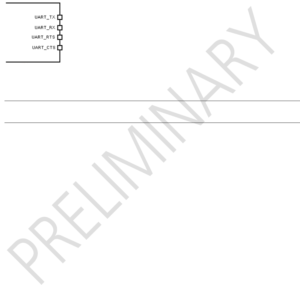
8.3 UART Interface
This is a standard UART interface for communicating with other serial devices.
CSR8811 UART interface provides a simple mechanism for communicating with other serial devices using the RS-232
protocol.
The above figure shows the 4 signals that implement the UART function. When BT830 is connected to another digital
device, UART_RX and UART_TX transfer data between the 2 devices. The remaining 2 signals, UART_CTS and
UART_RTS, implement RS232 hardware flow control where both are active low indicators. The default configuration
of UART is 115200 bauds; None parity check; 1 stop bit; 8 bits per byte.
Note: To communicate with the UART at its maximum data rate using a standard PC, an accelerated serial port
adapter card is required for the PC.
8.4 PCM Interface
The audio PCM interface on the BT830 supports:
Continuous transmission and reception of PCM encoded audio data over Bluetooth.
Processor overhead reduction through hardware support for continual transmission and reception of PCM
data.
A bidirectional digital audio interface that routes directly into the baseband layer of the firmware. It does not
pass through the HCI protocol layer.
Hardware on the BT830 for sending data to and from a SCO connection.
Up to three SCO connections on the PCM interface at any one time.
PCM interface master, generating PCM_SYNC and PCM_CLK.
PCM interface slave, accepting externally generated PCM_SYNC and PCM_CLK.
Various clock formats including:
- Long Frame Sync
- Short Frame Sync
GCI timing environments.
13-bit or 16-bit linear, 8-bit µ-law, or A-law companded sample formats.
Receives and transmits on any selection of three of the first four slots following PCM_SYNC.
The PCM configuration options are enabled by setting PSKEY_PCM_CONFIG32.
BT830 Hardware Integration Guide
Version 0.1 (PRELIMINARY)
Americas: +1-800-492-2320 Option 2
Europe: +44-1628-858-940
Hong Kong: +852-2923-0610
www.lairdtech.com/bluetooth
13
CONN-GUIDE-BT830
(PRELIMINARY)
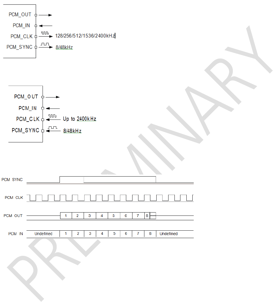
8.4.1 PCM Interface Master/Slave
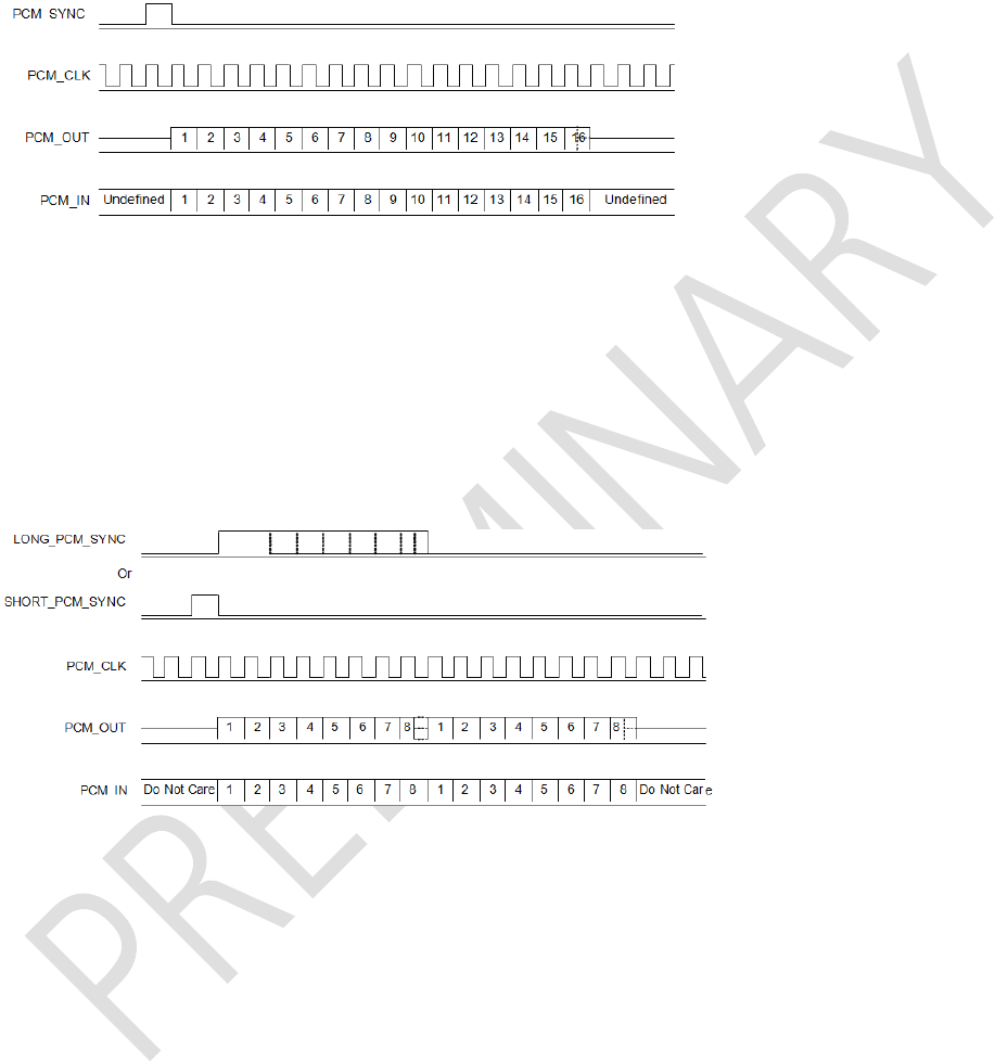
When configured as the master of the PCM interface, the BT830 generates PCM_CLK and PCM_SYNC.
Figure 2: PCM Interface Master
Figure 3: PCM Interface Slave
8.4.2
L
ong
Frame
Sync
Figure 4: Long Frame Sync (shown with 8-bit Companded Sample)
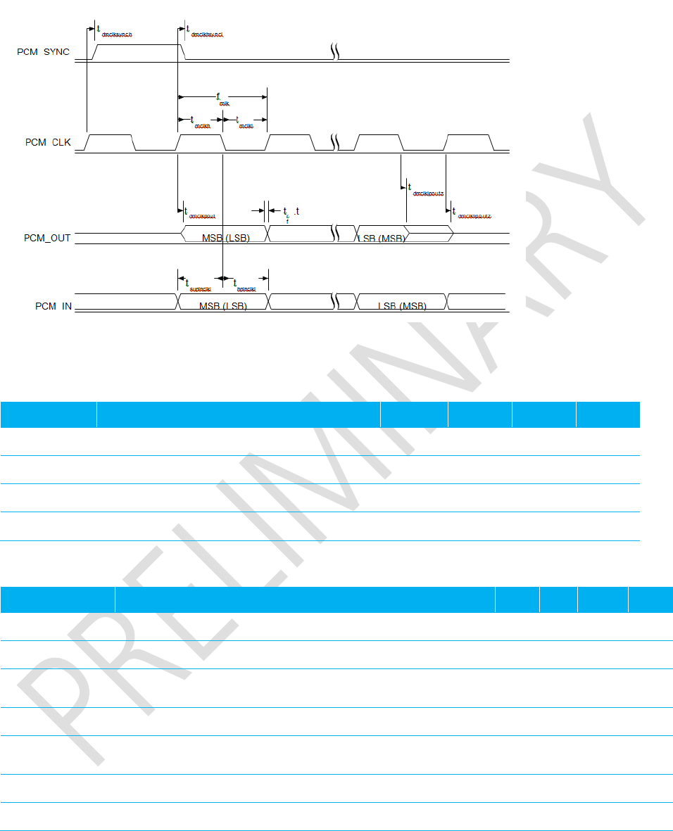
Long Frame Sync is the name given to a clocking format that controls the transfer of PCM data words or samples. In
Long Frame Sync, the rising edge of PCM_SYNC indicates the start of the PCM word. When the BT830 is configured
as PCM master, generating PCM_SYNC and PCM_CLK, then PCM_SYNC is eight bits long. When the BT830 is
configured as PCM Slave, PCM_SYNC is from one cycle PCM_CLK to half the PCM_SYNC rate.
BT830 samples PCM_IN on the falling edge of PCM_CLK and transmits PCM_OUT on the rising edge. PCM_OUT is
configurable as high impedance on the falling edge of PCM_CLK in the LSB position or on the rising edge.
BT830 Hardware Integration Guide
Version 0.1 (PRELIMINARY)
Americas: +1-800-492-2320 Option 2
Europe: +44-1628-858-940
Hong Kong: +852-2923-0610
www.lairdtech.com/bluetooth
14
CONN-GUIDE-BT830
(PRELIMINARY)
8.4.3
S
hort
Frame
S
y
nc
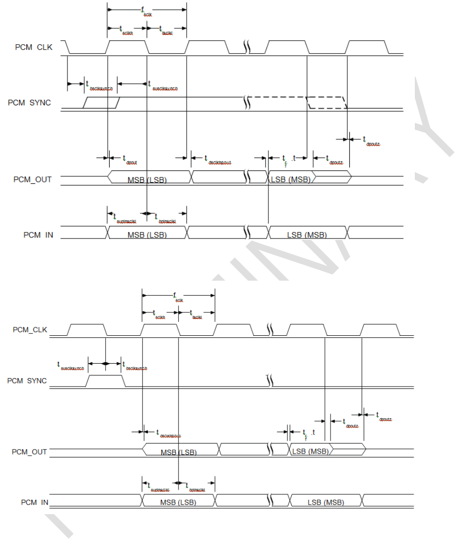
In Short Frame Sync, the falling edge of PCM_SYNC indicates the start of the PCM word. PCM_SYNC is always one
clock cycle long.
Figure 5: Short Frame Sync (Shown with 16-bit Sample)
As with Long Frame Sync, BT830 samples PCM_IN on the falling edge of PCM_CLK and transmits PCM_OUT on the
rising edge. PCM_OUT is configurable as high impedance on the falling edge of PCM_CLK in the LSB position or on
the rising edge.
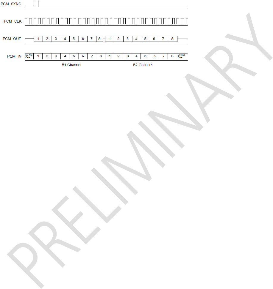
8.4.4 Multi-Slot Operation
More than 1 SCO connection over the PCM interface is supported using multiple slots. Up to 3 SCO connections are
carried over any of the first 4 slots.
Figure 6: Multi-slot Operation with 2 Slots and 8-bit Companded Samples
BT830 Hardware Integration Guide
Version 0.1 (PRELIMINARY)
Americas: +1-800-492-2320 Option 2
Europe: +44-1628-858-940
Hong Kong: +852-2923-0610
www.lairdtech.com/bluetooth
15
CONN-GUIDE-BT830
(PRELIMINARY)
8.5 GCI Interface
BT830 is compatible with the GCI, a standard synchronous 2B+D ISDN timing interface. The two 64 kbps B channels
are accessed when this mode is configured.
Figure 7: Multi-slot Operation
The start of frame is indicated by the rising edge of PCM_SYNC and runs at 8 kHz.
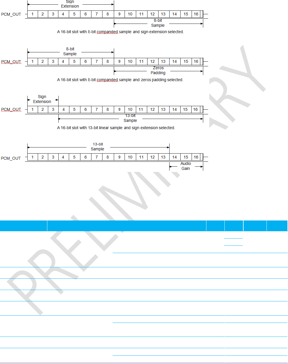
8.6 Slots and Sample Formats
BT830 receives and transmits on any selection of the first four slots following each sync pulse. Slot durations are
either 8 or 16 clock cycles:
8 clock cycles for 8-bit sample formats.
16 clock cycles for 8-bit, 13-bit, or 16-bit sample formats.
BT830 supports:
13-bit linear, 16-bit linear and 8-bit µ-law or A-law sample formats
A sample rate of 8 ksps
Little or big endian bit order
For 16-bit slots, the three or eight unused bits in each slot are filled with sign extension, padded with zeros or a
programmable 3-bit audio attenuation compatible with some codecs.
BT830 Hardware Integration Guide
Version 0.1 (PRELIMINARY)
Americas: +1-800-492-2320 Option 2
Europe: +44-1628-858-940
Hong Kong: +852-2923-0610
www.lairdtech.com/bluetooth
16
CONN-GUIDE-BT830
(PRELIMINARY)
Figure 8: 16-bit Slot Length and Sample Formats
8.7
PCM Timing Information
Table 10: PCM Timing information
Symbol
Parameter
Min
Typ
Max
Unit
fmclk
PCM_CLK frequency
4MHz DDS generation. Frequency
selection is programmable.
-
128
-
kHz
256
512
48MHz DDS generation. Frequency
selection is programmable.
2.9
-
-
kHz
-
PCM_SYNC frequency for SCO connection
-
8
-
kHz
tmclkh (a)
PCM_CLK high
4MHz DDS generation
980
-
-
ns
tmclkl a)
PCM_CLK low
4MHz DDS generation
730
-
-
ns
-
PCM_CLK jitter
48MHz DDS generation
-
-
21
ns
pk-pk
tdmclksynch
Delay time from
PCM_CLK high to
PCM_SYNC high
4MHz DDS generation
-
-
20
ns
48MHz DDS generation
-
-
40.83
ns
tdmclkpout
Delay time from PCM_CLK high to valid PCM_OUT
-
-
20
ns
tdmclklsyncl
Delay time from
PCM_CLK low to
4MHz DDS generation
-
-
20
ns
48MHz DDS generation
-
-
40.83
ns
BT830 Hardware Integration Guide
Version 0.1 (PRELIMINARY)
Americas: +1-800-492-2320 Option 2
Europe: +44-1628-858-940
Hong Kong: +852-2923-0610
www.lairdtech.com/bluetooth
17
CONN-GUIDE-BT830
(PRELIMINARY)
Symbol
Parameter
Min
Typ
Max
Unit
PCM_SYNC low (long
frame sync only)
(a) Assumes normal system clock operation. Figures vary during low-power modes, when system clock speeds are reduced.
Table 11: PCM Master Mode Timing Parameters
Symbol
Parameter
Min
Typ
Max
Unit
tdmclkhsyncl
Delay time from
PCM_CLK high to
PCM_SYNC low
4MHz DDS generation
-
-
20
ns
48MHz DDS generation
-
-
40.83
ns
tdmclklpoutz
Delay time from PCM_CLK low to PCM_OUT
high impedance
-
-
20
ns
tdmclkhpoutz
Delay time from PCM_CLK high to PCM_OUT
high impedance
-
-
20
ns
tsupinclkl
Set-up time for PCM_IN valid to PCM_CLK low
20
-
-
ns
thpinclkl
Hold time for PCM_CLK low to PCM_IN invalid
0
-
-
ns
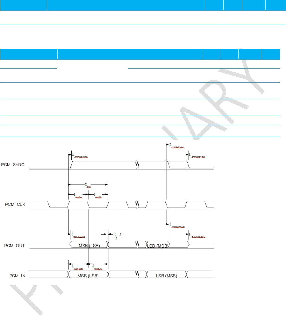
Figure 9: PCM Master Timing Long Frame Sync
BT830 Hardware Integration Guide
Version 0.1 (PRELIMINARY)
Americas: +1-800-492-2320 Option 2
Europe: +44-1628-858-940
Hong Kong: +852-2923-0610
www.lairdtech.com/bluetooth
18
CONN-GUIDE-BT830
(PRELIMINARY)
Figure 10: PCM Master Timing Short Frame Sync
8.8 PCM Slave Timing
Symbol
Parameter
Min
Typ
Max
Unit
fsclk
PCM clock frequency (Slave mode: input)
64
-
2048
kHz
fsclk
PCM clock frequency (GCI mode)
128
-
4096
kHz
tsclkl
PCM_CLK low time
200
-
-
ns
tsclkh
PCM_CLK high time
200
-
-
ns
8.9 PCM Slave Mode Timing Parameters
Symbol
Parameter
Min
Typ
Max
Unit
thsclksynch
Hold time from PCM_CLK low to PCM_SYNC high
2
-
-
ns
tsusclksynch
Set-up time for PCM_SYNC high to PCM_CLK low
20
-
-
ns
tdpout
Delay time from PCM_SYNC or PCM_CLK, whichever is later,
to valid PCM_OUT data (long frame sync only)
-
-
15
ns
tdsclkhpout
Delay time from CLK high to PCM_OUT valid data
-
-
15
ns
tdpoutz
Delay time from PCM_SYNC or PCM_CLK low, whichever is
later, to PCM_OUT data line high impedance
-
-
20
ns
tsupinsclkl
Set-up time for PCM_IN valid to CLK low
20
-
-
ns
thpinsclkl
Hold time for PCM_CLK low to PCM_IN invalid
2
-
-
ns
BT830 Hardware Integration Guide
Version 0.1 (PRELIMINARY)
Americas: +1-800-492-2320 Option 2
Europe: +44-1628-858-940
Hong Kong: +852-2923-0610
www.lairdtech.com/bluetooth
19
CONN-GUIDE-BT830
(PRELIMINARY)
Figure 11: PCM Slave Timing Long Frame Sync
Figure 12: PCM Slave Timing Short Frame Sync
BT830 Hardware Integration Guide
Version 0.1 (PRELIMINARY)
Americas: +1-800-492-2320 Option 2
Europe: +44-1628-858-940
Hong Kong: +852-2923-0610
www.lairdtech.com/bluetooth
20
CONN-GUIDE-BT830
(PRELIMINARY)
8.10 PCM_CLK and PCM_SYNC Generation
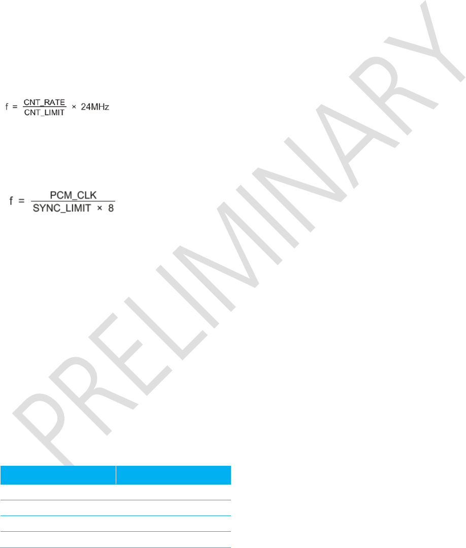
BT830 has two methods of generating PCM_CLK and PCM_SYNC in master mode:
Generating these signals by DDS from BT830internal 4MHz clock. Using this mode limits PCM_CLK to 128, 256
or 512 kHz and PCM_SYNC to 8 kHz.
Generating these signals by DDS from an internal 48MHz clock, which enables a greater range of frequencies
to be generated with low jitter but consumes more power. To select this second method set bit
48M_PCM_CLK_GEN_EN in PSKEY_PCM_CONFIG32. When in this mode and with long frame sync, the length
of PCM_SYNC is either 8 or 16 cycles of PCM_CLK, determined by LONG_LENGTH_SYNC_EN in
PSKEY_PCM_CONFIG32.
Equation 8.1 describes PCM_CLK frequency when generated from the internal 48MHz clock:
Equation 8.1: PCM_CLK Frequency Generated Using the Internal 48MHz Clock
Set the frequency of PCM_SYNC relative to PCM_CLK using Equation 8.2:
Equation 8.2: PCM_SYNC Frequency Relative to PCM_CLK
CNT_RATE, CNT_LIMIT and SYNC_LIMIT are set using PSKEY_PCM_LOW_JITTER_CONFIG. As an example, to
generate PCM_CLK at 512kHz with PCM_SYNC at 8kHz, set SKEY_PCM_LOW_JITTER_CONFIG to 0x08080177.
8.11 PCM Configuration
Configure the PCM by using PSKEY_PCM_CONFIG32 and PSKEY_PCM_LOW_JITTER_CONFIG (See your PSKey file).
The default for PSKEY_PCM_CONFIG32 is 0x00800000 (for example: first slot following sync is active, 13-bit linear
voice format, long frame sync and interface master generating 256kHz PCM_CLK from 4MHz internal clock with no
tri-state of PCM_OUT).
8.12 Digital Audio Interface (I²S)
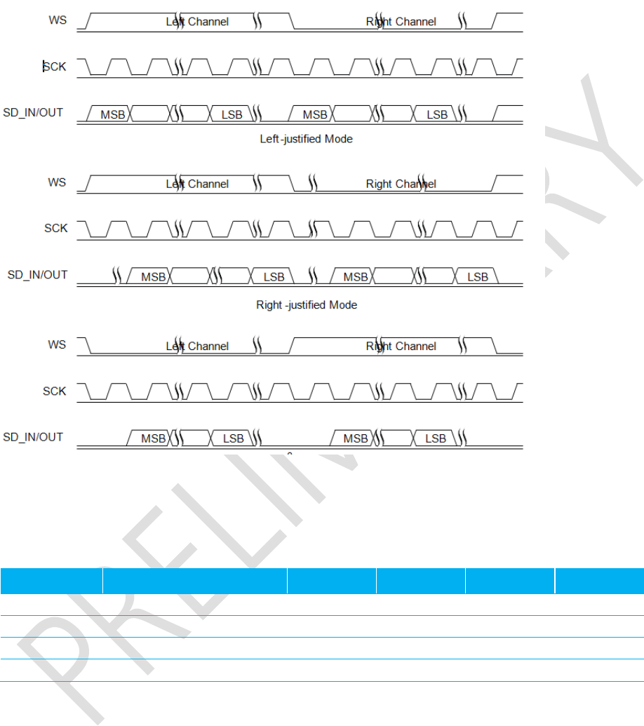
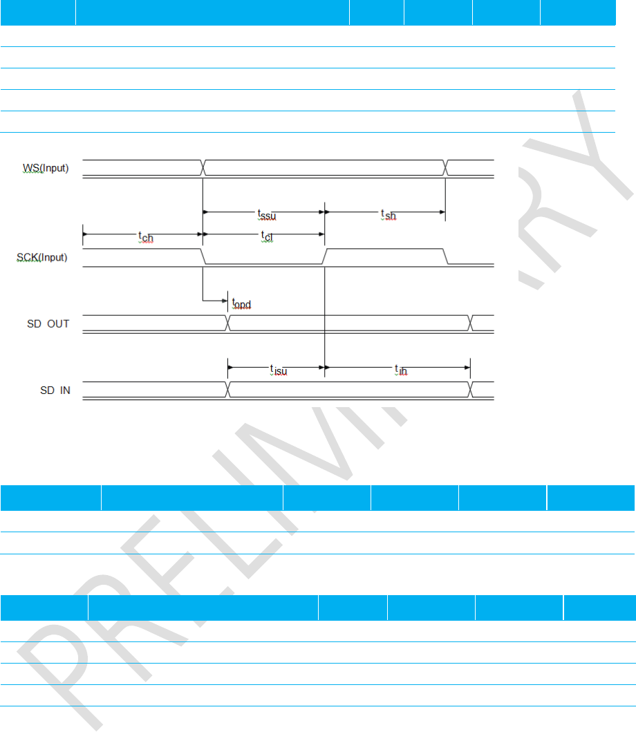
The digital audio interface supports the industry standard formats for I²S, left-justified or right-justified. The interface
shares the same pins as the PCM interface, which means each audio bus is mutually exclusive in its usage. Table 12
lists these alternative functions. Figure 11 shows the timing diagram.
Table 12: Alternative Functions of the Digital Audio Bus Interface on the PCM Interface.
PCM
Interface
I²S
Interface
PCM_OUT
SD_OUT
PCM_IN
SD_IN
PCM_SYNC
WS
PCM_CLK
SCK
BT830 Hardware Integration Guide
Version 0.1 (PRELIMINARY)
Americas: +1-800-492-2320 Option 2
Europe: +44-1628-858-940
Hong Kong: +852-2923-0610
www.lairdtech.com/bluetooth
21
CONN-GUIDE-BT830
(PRELIMINARY)
Configure the digital audio interface using PSKEY_DIGITAL_AUDIO_CONFIG, see BlueCore Audio API Specification
and the PS Key file.
Figure 13: PCM Configuration
The internal representation of audio samples within BT830is 16-bit and data on SD_OUT is limited to 16-bit per
channel.
Table 13: Digital Audio Interface Slave Timing
Symbol
Parameter
Min
Typ
Max
Unit
-
SCK Frequency
-
-
6.2
MHz
-
WS Frequency
-
-
96
kHz
tch
SCK high time
80
-
-
ns
tcl
SCK low time
80
-
-
ns
BT830 Hardware Integration Guide
Version 0.1 (PRELIMINARY)
Americas: +1-800-492-2320 Option 2
Europe: +44-1628-858-940
Hong Kong: +852-2923-0610
www.lairdtech.com/bluetooth
22
CONN-GUIDE-BT830
(PRELIMINARY)
Table 14: I²S Slave Mode Timing
Symbol
Parameter
Min
Typ
Max
Unit
tssu
WS valid to SCK high set-up time
20
-
-
ns
tsh
SCK high to WS invalid hold time
2.5
-
-
ns
topd
SCK low to SD_OUT valid delay time
-
-
20
ns
tisu
SD_IN valid to SCK high set-up time
20
-
-
ns
tih
SCK high to SD_IN invalid hold time
2.5
-
-
ns
Figure 14: Digital Audio Interface Slave Timing
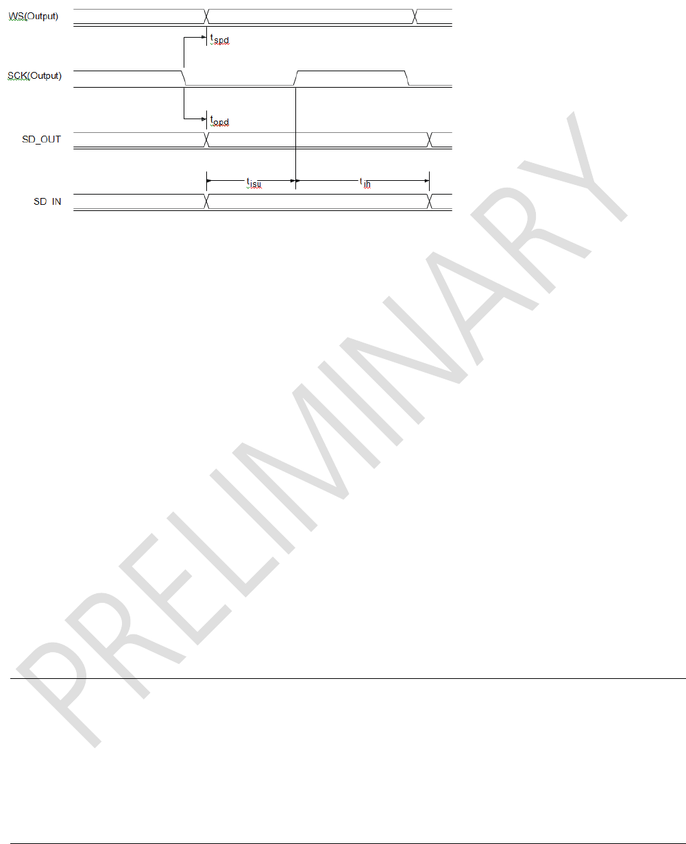
Table 15: Digital Audio Interface Master Timing
Symbol
Parameter
Min
Typ
Max
Unit
-
SCK Frequency
-
-
6.2
MHz
-
WS Frequency
-
-
96
kHz
Table 16: I²S Master Mode Timing Parameters, WS and SCK as Outputs
Symbol
Parameter
Min
Typ
Max
Unit
tspd
SCK low to WS valid delay time
-
-
39.27
ns
topd
SCK low to SD_OUT valid delay time
-
-
18.44
ns
tisu
SD_IN valid to SCK high set-up time
18.44
-
-
ns
tih
SCK high to SD_IN invalid hold time
0
-
-
ns
BT830 Hardware Integration Guide
Version 0.1 (PRELIMINARY)
Americas: +1-800-492-2320 Option 2
Europe: +44-1628-858-940
Hong Kong: +852-2923-0610
www.lairdtech.com/bluetooth
23
CONN-GUIDE-BT830
(PRELIMINARY)
Figure 15: Digital Audio Interface Master Timing
9 POWER SUPPLY AND REGULATION
See the Example Application Schematic (Error! Reference source not found.) for the regulator configuration. BT830
can be powered by either two sources listed below
Method #1: Apply 3.3 V on pin-9,High-voltage linear regulator input (VREG_IN_HV), to generate the main 1.8
V out put on pin-10 (VREG_OUT_HV).
A minimum 1.5μF capacitor must be connected to the Pin-10 (VREG_OUT_HV). Low ESR capacitors such as
multilayer ceramic types should be used.
Method #2: Apply 1.8V on pin-10 High-voltage linear regulator output (VREG_OUT_HV), to generate the
internal voltage for the system. Be sure to left Pin-9 un-connected in this method.
9.1 Voltage Regulator Enable and Reset
A single pin, VREG_EN_RST#, controls both the High-voltage linear regulator enables and the digital reset function.
The VREG_EN_RST# pin remains active controlling the reset function if the HV linear regulator is not used so the pin
must be driven high to take the device out of reset.
The regulator is enabled by taking the VREG_EN_RST# pin above 1V. The regulator can also be controlled by the
software.
The VREG_EN_RST# is also connected internally to the reset function, and is powered from the VDD_PADS supply, so
voltages above VDD_PADS must not be applied to this pin. The VREG_EN_RST# pin is pulled down internally.
The VREG_EN_RST# pin is an active low reset. Assert the reset signal for a period >5 ms to ensure a full reset.
Note: The regulator enables are released as soon as VREG_EN_RST# is low, so the regulators shut down.
Therefore do not take VREG_EN_RST# low for less than 5 ms, as a full reset is not guaranteed.
Other reset sources are:
Power-on reset
Via a software-configured watchdog timer
A warm reset function is also available under software control. After a warm reset the RAM data remains
available.
BT830 Hardware Integration Guide
Version 0.1 (PRELIMINARY)
Americas: +1-800-492-2320 Option 2
Europe: +44-1628-858-940
Hong Kong: +852-2923-0610
www.lairdtech.com/bluetooth
24
CONN-GUIDE-BT830
(PRELIMINARY)
9.2 Power Sequencing
CSR recommends that all power supplies are powered at the same time. The order of powering the supplies relative
to the I/O supply, VDD_PADS to VREG_IN_HV or VREG_OUT_HV, is not important.
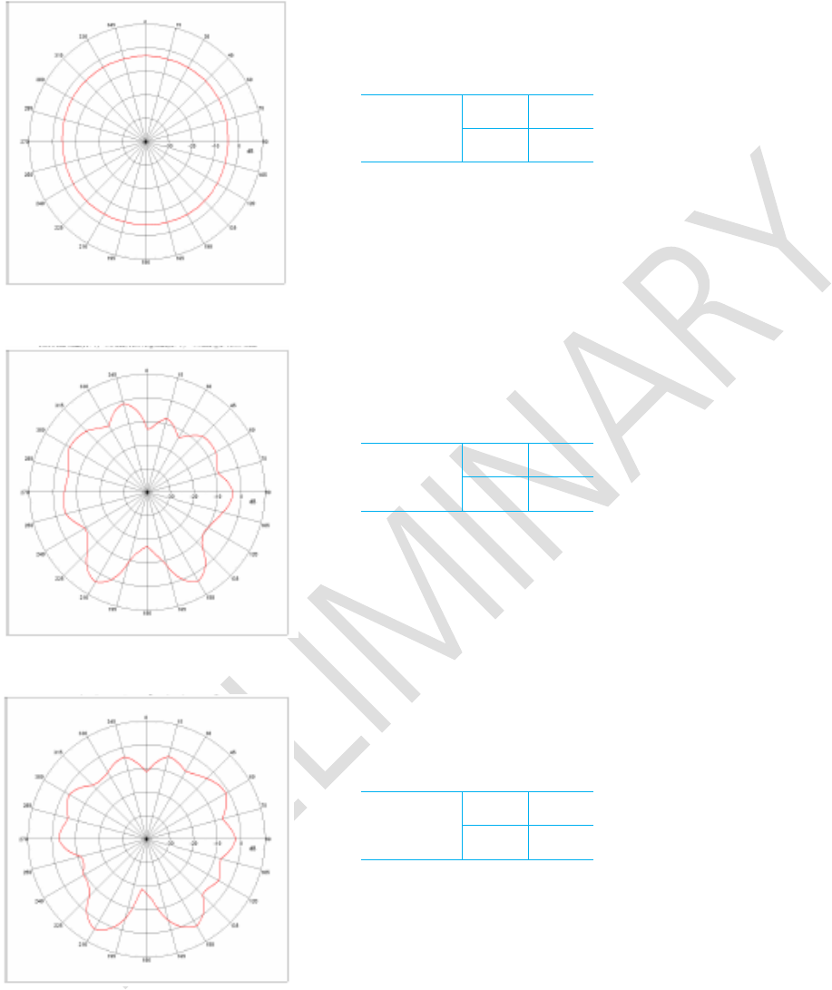
10 ANTENNA PERFORMANCE
Table 17 displays antenna performance for this module.
Table 17: Gain table
Unit in dBi @ 2.44 GHz
XY-plane
XZ-plane
YZ-plane
Efficiency
Peak
Avg.
Peak
Avg.
Peak
Avg.
A1
-3.5
-4.2
3.8
-5.3
3.2
-4.7
41.0%
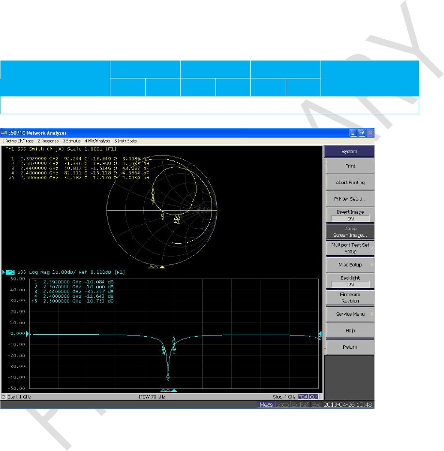
Figure 16: Network Analyzer output
BT830 Hardware Integration Guide
Version 0.1 (PRELIMINARY)
Americas: +1-800-492-2320 Option 2
Europe: +44-1628-858-940
Hong Kong: +852-2923-0610
www.lairdtech.com/bluetooth
25
CONN-GUIDE-BT830
(PRELIMINARY)
Figure 17: XY plane
XY-plane
Peak
Avg.
-3.5
-4.2
Figure 18: XZ-plane
XZ-plane
Peak
Avg.
3.8
-5.3
Figure 19: YZ-plane
YZ-plane
Peak
Avg.
3.2
-4.7
BT830 Hardware Integration Guide
Version 0.1 (PRELIMINARY)
Americas: +1-800-492-2320 Option 2
Europe: +44-1628-858-940
Hong Kong: +852-2923-0610
www.lairdtech.com/bluetooth
26
CONN-GUIDE-BT830
(PRELIMINARY)
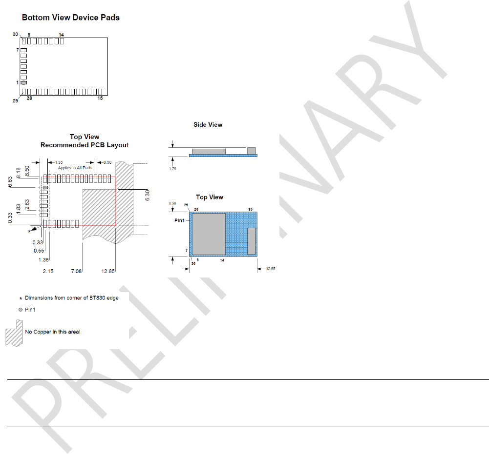
11 MECHANICAL DIMENSIONS AND LAND PATTERN
11.1 BT830 Mechanical Drawing
Note: Dimensions are in mm.
Tolerances: .xx ±0.03 mm
.x ±1.3 mm
BT830 Hardware Integration Guide
Version 0.1 (PRELIMINARY)
Americas: +1-800-492-2320 Option 2
Europe: +44-1628-858-940
Hong Kong: +852-2923-0610
www.lairdtech.com/bluetooth
27
CONN-GUIDE-BT830
(PRELIMINARY)
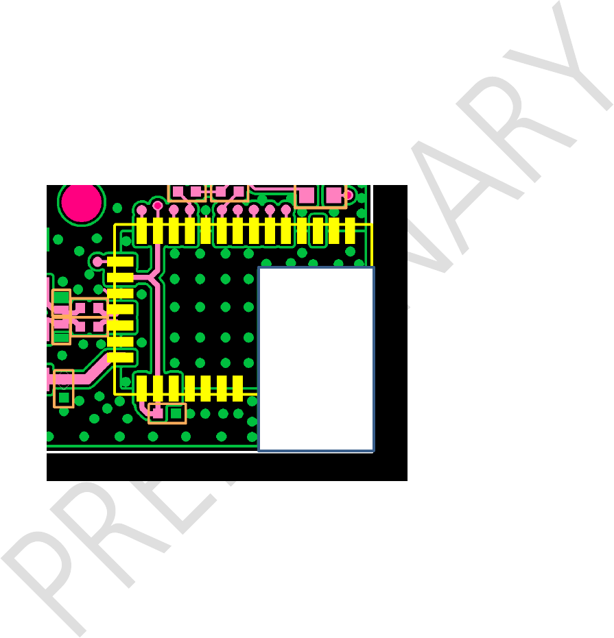
12 IMPLEMENTATION NOTE
12.1 PCB Layout on Host PCB
Checklist (for PCB):
MUST locate the BT830 module close to the edge of PCB.
Use solid GND plane on inner layer (for best EMC and RF performance).
Place GND vias close to module GND pads as possible
Route traces to avoid noise being picked up on VCC supply.
Antenna Keep-out area:
- Ensure there is no copper in the antenna keep-out area on any layers of the host PCB.
- Keep all mounting hardware and metal clear of the area to allow proper antenna radiation.
- For best antenna performance, place the BT830 module on the edge of the host PCB, preferably in the
corner with the antenna facing the corner.
- A different host PCB thickness dielectric will have small effect on antenna.
Figure 20: Recommend Antenna keep-out area (in White) used on the BT830
12.1.1 Antenna Keep-out and Proximity to Metal or Plastic
Checklist (for metal /plastic enclosure):
Minimum safe distance for metals without seriously compromising the antenna (tuning) is 40 mm top/bottom
and 30 mm left or right.
Metal close to the BT830 chip monopole antenna (bottom, top, left, right, any direction) will have degradation
on the antenna performance. The amount of degradation is entirely system dependent which means some
testing by customers is required (in their host application).
Any metal closer than 20 mm starts to significantly degrade performance (S11, gain, radiation efficiency).
It is best that the customer tests the range with mock-up (or actual prototype) of the product to assess effects
of enclosure height (and material whether metal or plastic).
BT830 Hardware Integration Guide
Version 0.1 (PRELIMINARY)
Americas: +1-800-492-2320 Option 2
Europe: +44-1628-858-940
Hong Kong: +852-2923-0610
www.lairdtech.com/bluetooth
28
CONN-GUIDE-BT830
(PRELIMINARY)
12.1.2 DC power supply options for using BT830 module
Using DC power 3.3 V
Power the on Pin-9 (VREG_IN_HV) with 3.3 V and pull-high on Pin-8 (VREG_EN_RST#) to turn on the internal
regulator. The BT830 module generates 1.8 V output on Pin-10 (VREG_OUT_HV) which can supply to the other
DC pin of the board.
Using DC power 1.8 V
Leave the Pin-9 (VREG_IN_HV) no connection, power the Pin-10 (VREG_OUT_HV) with 1.8 V and pull-high on
Pin-8 (VREG_EN_RST#) to turn on the internal regulator.
13 APPLICATION NOTE FOR SURFACE MOUNT MODULES
13.1 Introduction
Laird surface mount modules are designed to conform to all major manufacturing guidelines. This application note is
intended to provide additional guidance beyond the information that is presented in the user manual. This application
note is considered a living document and is updated as new information is presented.
The modules are designed to meet the needs of a number of commercial and industrial applications. They are easy to
manufacture and they conform to current automated manufacturing processes.
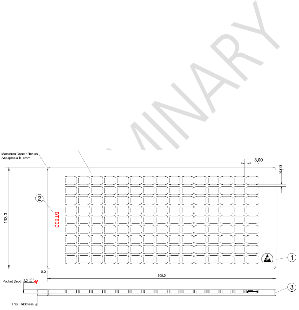
13.2 Shipping tray
Modules are shipped in ESD (Electrostatic Discharge) safe trays that can be loaded into most manufacturers pick and
place machines. Layouts of the trays are provided in Figure 21.
Figure 21: Shipping tray layout
BT830 Hardware Integration Guide
Version 0.1 (PRELIMINARY)
Americas: +1-800-492-2320 Option 2
Europe: +44-1628-858-940
Hong Kong: +852-2923-0610
www.lairdtech.com/bluetooth
29
CONN-GUIDE-BT830
(PRELIMINARY)
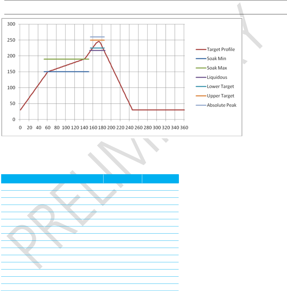
13.3 Reflow Parameters
Laird surface mount modules are designed to be easily manufactured, including reflow soldering to a PCB. Ultimately
it is the responsibility of the customer to choose the appropriate solder paste and to ensure oven temperatures during
reflow meet the requirements of the solder paste. Laird’s surface mount modules conform to J-STD-020D1 standards
for reflow temperatures.
Important: During reflow, modules should not be above 260° and not for more than 30 seconds.
Figure 13-22: Recommended Reflow Temperature
Temperatures should not exceed the minimums or maximums presented in Table 18.
Table 18: Recommended Maximum and minimum temperatures
Specification
Value
Unit
Temperature Inc./Dec. Rate (max)
1~3
°C / Sec
Temperature Decrease rate (goal)
2-4
°C / Sec
Soak Temp Increase rate (goal)
.5 - 1
°C / Sec
Flux Soak Period (Min)
70
Sec
Flux Soak Period (Max)
120
Sec
Flux Soak Temp (Min)
150
°C
Flux Soak Temp (max)
190
°C
Time Above Liquidous (max)
70
Sec
Time Above Liquidous (min)
50
Sec
Time In Target Reflow Range (goal)
30
Sec
Time At Absolute Peak (max)
5
Sec
Liquidous Temperature (SAC305)
218
°C
Lower Target Reflow Temperature
240
°C
Upper Target Reflow Temperature
250
°C
Absolute Peak Temperature
260
°C

BT830 Hardware Integration Guide
Version 0.1 (PRELIMINARY)
Americas: +1-800-492-2320 Option 2
Europe: +44-1628-858-940
Hong Kong: +852-2923-0610
www.lairdtech.com/bluetooth
30
CONN-GUIDE-BT830
(PRELIMINARY)
14 FCC AND IC REGULATORY
Model
US/FCC
CANADA/IC
BT830
TBC
TBC
BT830
TBC
TBC
DVK-BT830
TBC
TBC
The BT830 family has been designed to operate with the antenna listed below having a maximum gain of 0.5 dBi. The
required antenna impedance is 50 ohms.
Item
Part Number
Mfg.
Type
Gain (dBi)
1
AT3216-B2R7HAA
ACX
Ceramic
0.5
14.1 Documentation Requirements
In order to ensure regulatory compliance, when integrating the BT830 into a host device, it is necessary to meet the
documentation requirements set forth by the applicable regulatory agencies. The following sections (FCC, Industry
Canada, and European Union) outline the information that may be included in the user’s guide and external labels for
the host devices into which the BT830 is integrated.
FCC
Note: You must place “Contains FCC ID: TBC” on the host product in such a location that it can be seen by an
operator at the time of purchase.
User’s Guide Requirements
The BT830 complies with FCC Part 15 Rules for a Modular Approval. To leverage Laird’s grant, the conditions below
must be met for the host device into which the BT830 is integrated:
The transmitter module is not co-located with any other transmitter or antenna that is capable of simultaneous
operation.
As long as the conditions above are met, further transmitter testing is typically not required. However, the OEM
integrator is still responsible for testing its end-product for any additional compliance requirements required with this
module installed, such as (but not limited to) digital device emissions and PC peripheral requirements.
IMPORTANT:
In the event that the conditions above cannot be met (for example certain device configurations or
co-location with another transmitter), then the FCC authorization is no longer considered valid and the
FCC ID cannot be used on the final product. In these circumstances, the OEM integrator will be
responsible for re-evaluating the end product (including the transmitter) and obtaining a separate FCC
authorization.
When using Laird’s FCC grant for the BT830, the integrator must include specific information in the
user’s guide for the device into which the BT830 is integrated. The integrator must not provide
information to the end user regarding how to install or remove this RF module in the user’s manual of
the device into which the BT830 is integrated. The following FCC statements must be added in their
entirety and without modification into a prominent place in the user’s guide for the device into which
the BT830 is integrated:

BT830 Hardware Integration Guide
Version 0.1 (PRELIMINARY)
Americas: +1-800-492-2320 Option 2
Europe: +44-1628-858-940
Hong Kong: +852-2923-0610
www.lairdtech.com/bluetooth
31
CONN-GUIDE-BT830
(PRELIMINARY)
IMPORTANT NOTE: To comply with FCC requirements, the BT830 must not be co-located or
operating in conjunction with any other antenna or transmitter.
Federal Communication Commission Interference Statement
This equipment has been tested and found to comply with the limits for a Class B digital device,
pursuant to Part 15 of the FCC Rules. These limits are designed to provide reasonable protection against
harmful interference in a residential installation. This equipment generates, uses, and can radiate radio
frequency energy and, if not installed and used in accordance with the instructions, may cause harmful
interference to radio communications. However, there is no guarantee that interference will not occur
in a particular installation. If this equipment does cause harmful interference to radio or television
reception, which can be determined by turning the equipment off and on, the user is encouraged to try
to correct the interference by one of the following measures:
1. Reorient or relocate the receiving antenna.
2. Increase the separation between the equipment and receiver.
3. Connect the equipment into an outlet on a circuit different from that to which the receiver is
connected.
4. Consult the dealer or an experienced radio/TV technician for help.
FCC Caution: Any changes or modifications not expressly approved by the party responsible for
compliance could void the user's authority to operate this equipment.
This device complies with Part 15 of the FCC Rules. Operation is subject to the following two
conditions: (1) This device may not cause harmful interference, and (2) this device must accept any
interference received, including interference that may cause undesired operation.
IMPORTANT NOTE: FCC Radiation Exposure Statement:
This equipment complies with FCC radiation exposure limits set forth for an uncontrolled environment.
Industry Canada
Note: You must place “Contains IC ID: TBC” on the host product in such a location that it can be seen by an
operator at the time of purchase.
RF Radiation Hazard Warning
Using higher gain antennas and types of antennas not certified for use with this product is not allowed. The device
shall not be co-located with another transmitter.
Cet avertissement de sécurité est conforme aux limites d'exposition définies par la norme CNR-102 at relative aux
fréquences radio.
This radio transmitter (Contains IC ID: TBC) has been approved by Industry Canada to operate with the antenna types
listed in table above with the maximum permissible gain and required antenna impedance for each antenna type
indicated. Antenna types not included in this list, having a gain greater than the maximum gain indicated for that
type, are strictly prohibited for use with this device.
Le présent émetteur radio (Contains IC ID: TBC) a été approuvé par Industrie Canada pour fonctionner avec les types
d'antenne énumérés ci-dessous et ayant un gain admissible maximal et l'impédance requise pour chaque type
d'antenne. Les types d'antenne non inclus dans cette liste, ou dont le gain est supérieur au gain maximal indiqué,
sont strictement interdits pour l'exploitation de l'émetteur.

BT830 Hardware Integration Guide
Version 0.1 (PRELIMINARY)
Americas: +1-800-492-2320 Option 2
Europe: +44-1628-858-940
Hong Kong: +852-2923-0610
www.lairdtech.com/bluetooth
32
CONN-GUIDE-BT830
(PRELIMINARY)
Under Industry Canada regulations, this radio transmitter may only operate using an antenna of a type and maximum
(or lesser) gain approved for the transmitter by Industry Canada. To reduce potential radio interference to other users,
the antenna type and its gain should be so chosen that the equivalent isotropically radiated power (e.i.r.p.) is not
more than that necessary for successful communication.
Conformément à la réglementation d'Industrie Canada, le présent émetteur radio peut fonctionner avec une antenne
d'un type et d'un gain maximal (ou inférieur) approuvé pour l'émetteur par Industrie Canada. Dans le but de réduire
les risques de brouillage radioélectrique à l'intention des autres utilisateurs, il faut choisir le type d'antenne et son gain
de sorte que la puissance isotrope rayonnée équivalente (p.i.r.e.) ne dépasse pas l'intensité nécessaire à
l'établissement d'une communication satisfaisante.
This device complies with Industry Canada license-exempt RSS standard(s). Operation is subject to the following two
conditions: (1) this device may not cause interference, and (2) this device must accept any interference, including
interference that may cause undesired operation of the device.
Le présent appareil est conforme aux CNR d'Industrie Canada applicables aux appareils radio exempts de licence.
L'exploitation est autorisée aux deux conditions suivantes : (1) l'appareil ne doit pas produire de brouillage, et (2)
l'utilisateur de l'appareil doit accepter tout brouillage radioélectrique subi, même si le brouillage est susceptible d'en
compromettre le fonctionnement.
15 EUROPEAN UNION REGULATORY
The BT830 has been tested for compliance with relevant standards for the EU market. BT830 module was tested with
a 0.5 dBi chip antenna.
The OEM should consult with a qualified test house before entering their device into an EU member country to make
sure all regulatory requirements have been met for their complete device.
Reference the Declaration of Conformities listed below for a full list of the standards that the modules were tested to.
Test reports are available upon request.

BT830 Hardware Integration Guide
Version 0.1 (PRELIMINARY)
Americas: +1-800-492-2320 Option 2
Europe: +44-1628-858-940
Hong Kong: +852-2923-0610
www.lairdtech.com/bluetooth
33
CONN-GUIDE-BT830
(PRELIMINARY)
15.1 EU Declarations of Conformity
15.1.1 BT830
Manufacturer:
Laird
Product:
BT830-SA / BT830-ST
EU Directive:
RTTE 1995/5/EC
Conformity Assessment:
Annex IV
Reference standards used for presumption of conformity:
Article
Number
Requirement
Reference standard(s)
3.1a
Health and Safety
EN60950-1:2006+A11:2009+A1:2010+A12:2011
3.1b
Protection requirements with respect to
electromagnetic compatibility
EN 301 489-1 V1.9.2 (2011-09)
EN 301 489-17 V2.2.1 (2012-09)
Emissions:
EN55022:2006/A1:2007 (Class B)
Immunity:
EN61000-4-2:2009
EN61000-4-3:2006/A1:2008/A2:2010
3.2
Means of the efficient use of the radio
frequency spectrum
EN 300 328 V1.8.1 (2012-06)
Declaration:
We, Laird, declare under our sole responsibility that the essential radio test suites have been carried out and that the
above product to which this declaration relates is in conformity with all the applicable essential requirements of
Article 3 of the EU Directive 1999/5/EC, when used for its intended purpose.
Place of Issue:
Laird
Saturn House, Mercury Park
Wooburn Green
HP100HH,
United Kingdom
tel: +44 (0)1628 858 940
fax: +44 (0)1628 528 382
Date of Issue:
July 2013
Name of Authorized Person:
Andrew Dobbing, Engineering Manager
Signature:
16 ORDERING INFORMATION
Part Number
Description
BT830-SA
BTv4.0 Dual Mode UART HCI Module with integrated Antenna
BT830-ST
BTv4.0 Dual Mode UART HCI Module
DVK-BT830
Development Kit for BT830 Module
16.1 General Comments
This is a preliminary datasheet. Please check with Laird for the latest information before commencing a design. If in
doubt, ask.
BT830 Hardware Integration Guide
Version 0.1 (PRELIMINARY)
Americas: +1-800-492-2320 Option 2
Europe: +44-1628-858-940
Hong Kong: +852-2923-0610
www.lairdtech.com/bluetooth
34
CONN-GUIDE-BT830
(PRELIMINARY)
17 BLUETOOTH SIG APPROVALS
17.1 Application Note: Subsystem Combinations
This application note covers the procedure for generating a new Declaration ID for a Subsystem combination on the
Bluetooth SIG website. In the instance of subsystems, a member can combine two or more subsystems to create a
complete Bluetooth End Product solution.
Subsystem listings referenced as an example:
Design Name
Owner
Declaration ID
Link to listing on the SIG website
BT830
Laird
TBC
https://www.bluetooth.org/tpg/QLI_viewQDL.cfm?qid=TBC
Windows 8
(Host Subsystem)
Microsoft
Corporation
B012854
https://www.bluetooth.org/tpg/QLI_viewQDL.cfm?qid=12854
Laird Customer Declaration ID Procedure
This procedure assumes that the member is simply combining two subsystems to create a new design, without any
modification to the existing, qualified subsystems. This is achieved by using the Listing interface on the Bluetooth SIG
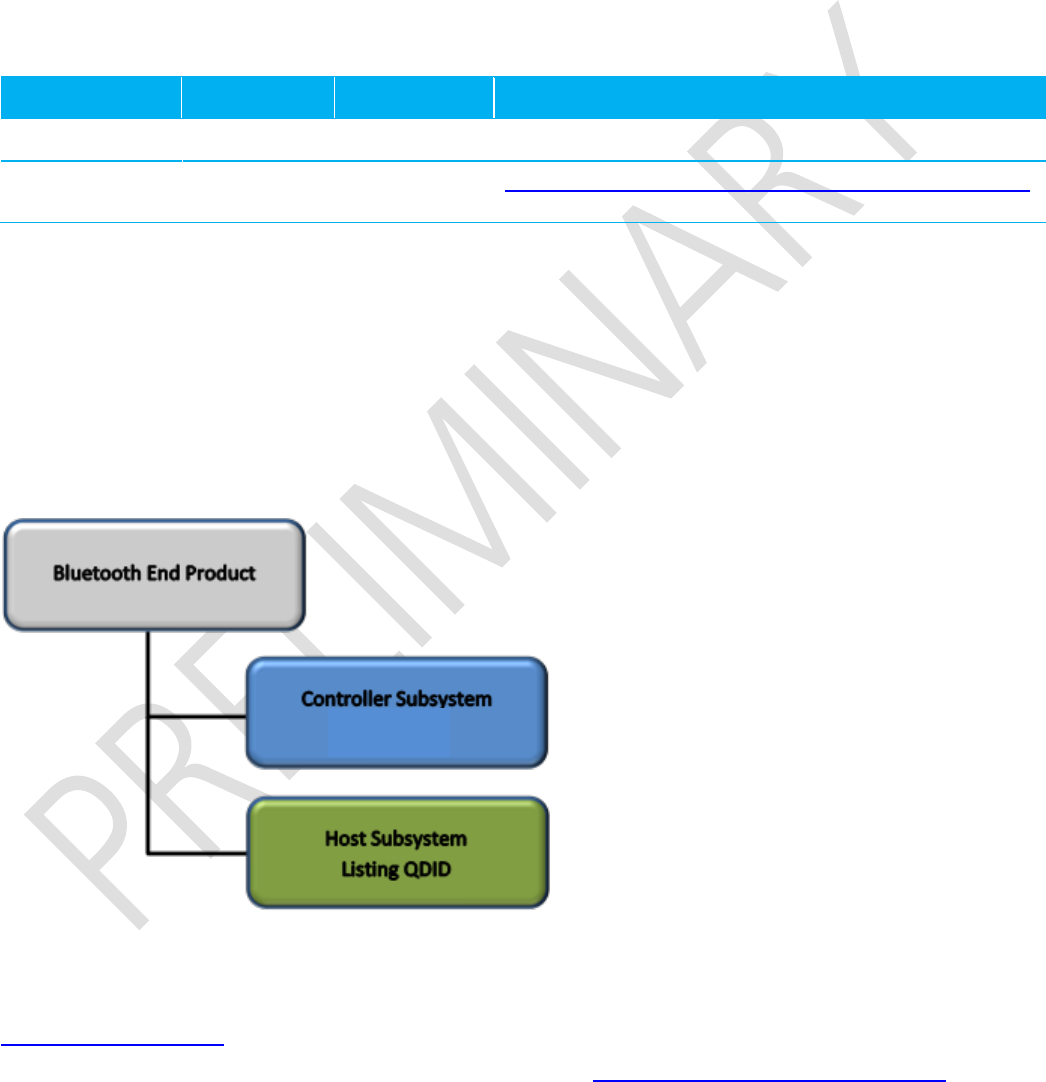
website. Figure 23 shows the basic subsystem combination of a controller and host subsystem. The Controller
provides the RF/BB/LM and HCI layers, with the Host providing L2CAP, SDP, GAP, RFCOMM/SPP and any other
specific protocols and profiles existing in the Host subsystem listing. The design may also include a Profile Subsystem.
The controller provides the RF/BB/LM and HCI layers, with the Host providing L2CAP, SDP, GAP, RFCOMM/SPP and
any other specific protocols and profiles existing in the Host subsystem listing. The design may also include a Profile
Subsystem.
Figure 23: Basic subsystem combination of a controller and host subsystem
The Qualification Process requires each company to registered as a member of the Bluetooth SIG –
http://www.bluetooth.org
The following link provides a link to the Bluetooth Registration page: https://www.bluetooth.org/login/register/
TBC

BT830 Hardware Integration Guide
Version 0.1 (PRELIMINARY)
Americas: +1-800-492-2320 Option 2
Europe: +44-1628-858-940
Hong Kong: +852-2923-0610
www.lairdtech.com/bluetooth
35
CONN-GUIDE-BT830
(PRELIMINARY)
For each Bluetooth Design it is necessary to purchase a Declaration ID. This can be done before starting the new
qualification, either through invoicing or credit card payment. The fees for the Declaration ID will depend on your
membership status, please refer to the following webpage:
https://www.bluetooth.org/en-us/test-qualification/qualification-overview/fees
For a detailed procedure of how to obtain a new Declaration ID for your design, please refer to the following SIG
document:
https://www.bluetooth.org/DocMan/handlers/DownloadDoc.ashx?doc_id=283698&vId=317486
To start the listing, go to: https://www.bluetooth.org/tpg/QLI_SDoc.cfm.
In step 1, select the option, Reference a Qualified Design and enter the Declaration IDs of each subsystem used in the
End Product design. You can then select your pre-paid Declaration ID from the drop down menu or go to the
Purchase Declaration ID page, (please note that unless the Declaration ID is pre-paid or purchased with a credit card,
it will not be possible to proceed until the SIG invoice is paid.
Once all the relevant sections of step 1 are finished, complete steps 2, 3, and 4 as described in the help document.
Your new Design will be listed on the SIG website and you can print your Certificate and DoC.
For further information please refer to the following training material:
https://www.bluetooth.org/en-us/test-qualification/qualification-overview/listing-process-updates
17.2 Additional Assistance
Please contact your local sales representative or our support team for further assistance:
Laird Technologies Connectivity Products Business Unit
Support Centre: http://ews-support.lairdtech.com
Email: wireless.support@lairdtech.com
Phone: Americas: +1-800-492-2320 Option 2
Europe: +44-1628-858-940
Hong Kong: +852 2923 0610
Web: http://www.lairdtech.com/bluetooth

BT830 Hardware Integration Guide
Version 0.1 (PRELIMINARY)
Americas: +1-800-492-2320 Option 2
Europe: +44-1628-858-940
Hong Kong: +852-2923-0610
www.lairdtech.com/bluetooth
36
CONN-GUIDE-BT830
(PRELIMINARY)
Copyright © 2014 Laird Technologies, Inc. All rights reserved.
The information contained in this manual and the accompanying software programs are copyrighted and all rights are reserved by Laird
Technologies, Inc. Laird Technologies, Inc. reserves the right to make periodic modifications of this product without obligation to notify any
person or entity of such revision. Copying, duplicating, selling, or otherwise distributing any part of this product or accompanying
documentation/software without the prior consent of an authorized representative of Laird Technologies, Inc. is strictly prohibited.
All brands and product names in this publication are registered trademarks or trademarks of their respective holders.
This material is preliminary Information furnished by Laird Technologies in this specification is believed to be accurate. Devices sold by Laird
Technologies are covered by the warranty and patent indemnification provisions appearing in its Terms of Sale only. Laird Technologies makes
no warranty, express, statutory, and implied or by description, regarding the information set forth herein. Laird Technologies reserves the right
to change specifications at any time and without notice. Laird Technologies’ products are intended for use in normal commercial and
industrial applications. Applications requiring unusual environmental requirements such as military, medical life-support or life-sustaining
equipment are specifically not recommended without additional testing for such application.
Limited Warranty, Disclaimer, Limitation of Liability
2006/8/16 v1.0
Federal Communication Commission Interference Statement
This equipment has been tested and found to comply with the limits for a Class B
digital device, pursuant to Part 15 of the FCC Rules. These limits are designed to
provide reasonable protection against harmful interference in a residential installation.
This equipment generates, uses and can radiate radio frequency energy and, if not
installed and used in accordance with the instructions, may cause harmful
interference to radio communications. However, there is no guarantee that
interference will not occur in a particular installation. If this equipment does cause
harmful interference to radio or television reception, which can be determined by
turning the equipment off and on, the user is encouraged to try to correct the
interference by one of the following measures:
- Reorient or relocate the receiving antenna.
- Increase the separation between the equipment and receiver.
- Connect the equipment into an outlet on a circuit different from that
to which the receiver is connected.
- Consult the dealer or an experienced radio/TV technician for help.
FCC Caution: Any changes or modifications not expressly approved by the party
responsible for compliance could void the user's authority to operate this equipment.
This device complies with Part 15 of the FCC Rules. Operation is subject to the
following two conditions: (1) This device may not cause harmful interference, and (2)
this device must accept any interference received, including interference that may
cause undesired operation.
IMPORTANT NOTE:
FCC Radiation Exposure Statement:
The product comply with the US portable RF exposure limit set forth for an
uncontrolled environment and are safe for intended operation as described in this
manual. The further RF exposure reduction can be achieved if the product can be
kept as far as possible from the user body or set the device to lower output power if
such function is available.
This transmitter must not be co-located or operating in conjunction with any other
antenna or transmitter.

2006/8/16 v1.0
This device is intended only for OEM integrators under the following
conditions:
1) The transmitter module may not be co-located with any other transmitter or
antenna,
As long as 1 condition above is met, further transmitter test will not be required.
However, the OEM integrator is still responsible for testing their end-product for any
additional compliance requirements required with this module installed
IMPORTANT NOTE
In the event that these conditions can not be met (for example certain laptop
configurations or co-location with another transmitter), then the FCC authorization is
no longer considered valid and the FCC ID can not be used on the final product. In
these circumstances, the OEM integrator will be responsible for re-evaluating the
end product (including the transmitter) and obtaining a separate FCC authorization.
End Product Labeling
The final end product must be labeled in a visible area with the following: “Contains
FCC ID: SQGBT830
Manual Information to the End User
The OEM integrator has to be aware not to provide information to the end user
regarding how to install or remove this RF module in the user’s manual of the end
product which integrates this module.
The end user manual shall include all required regulatory information/warning as
show in this manual.
2006/8/16 v1.0
Industry Canada statement:
This device complies with Industry Canada licence-exempt RSS standard(s). Operation is
subject to the following two conditions:
(1) this device may not cause interference, and
(2) this device must accept any interference, including interference that may cause
undesired operation of the device.
Le présent appareil est conforme aux CNR d'Industrie Canada applicables aux appareils
radio exempts de licence. L'exploitation est autorisée aux deux conditions suivantes :
(1) l'appareil ne doit pas produire de brouillage, et
(2) l'utilisateur de l'appareil doit accepter tout brouillage radioélectrique subi, même si le
brouillage est susceptible d'en compromettre le fonctionnement.
Radiation Exposure Statement:
The product comply with the Canada portable RF exposure limit set forth for an
uncontrolled environment and are safe for intended operation as described in this manual.
The further RF exposure reduction can be achieved if the product can be kept as far as
possible from the user body or set the device to lower output power if such function is
available.
Déclaration d'exposition aux radiations:
Le produit est conforme aux limites d'exposition pour les appareils portables RF pour les
Etats-Unis et le Canada établies pour un environnement non contrôlé. Le produit est sûr
pour un fonctionnement tel que décrit dans ce manuel. La réduction aux expositions RF
peut être augmentée si l'appareil peut être conservé aussi loin que possible du corps de
l'utilisateur ou que le dispositif est réglé sur la puissance de sortie la plus faible si une telle
fonction est disponible.

2006/8/16 v1.0
This device is intended only for OEM integrators under the following conditions:
1) The transmitter module may not be co-located with any other transmitter or antenna.
As long as 1 condition above are met, further transmitter test will not be required. However,
the OEM integrator is still responsible for testing their end-product for any additional
compliance requirements required with this module installed.
Cet appareil est conçu uniquement pour les intégrateurs OEM dans les conditions
suivantes:
1) Le module émetteur peut ne pas être coïmplanté avec un autre émetteur ou antenne.
Tant que les 1 condition ci-dessus sont remplies, des essais supplémentaires sur
l'émetteur ne seront pas nécessaires. Toutefois, l'intégrateur OEM est toujours
responsable des essais sur son produit final pour toutes exigences de conformité
supplémentaires requis pour ce module installé.
IMPORTANT NOTE:
In the event that these conditions can not be met (for example certain laptop
configurations or co-location with another transmitter), then the Canada authorization is no
longer considered valid and the IC ID can not be used on the final product. In these
circumstances, the OEM integrator will be responsible for re-evaluating the end product
(including the transmitter) and obtaining a separate Canada authorization.
NOTE IMPORTANTE:
Dans le cas où ces conditions ne peuvent être satisfaites (par exemple pour certaines
configurations d'ordinateur portable ou de certaines co-localisation avec un autre
émetteur), l'autorisation du Canada n'est plus considéré comme valide et l'ID IC ne peut
pas être utilisé sur le produit final. Dans ces circonstances, l'intégrateur OEM sera chargé
de réévaluer le produit final (y compris l'émetteur) et l'obtention d'une autorisation distincte
au Canada.
End Product Labeling
The final end product must be labeled in a visible area with the following: “Contains IC:
3147A-BT830”.
Plaque signalétique du produit final
Le produit final doit être étiqueté dans un endroit visible avec l'inscription suivante:
"Contient des IC: 3147A-BT830".
2006/8/16 v1.0
Manual Information to the End User
The OEM integrator has to be aware not to provide information to the end user regarding
how to install or remove this RF module in the user’s manual of the end product which
integrates this module.
The end user manual shall include all required regulatory information/warning as show in
this manual.
Manuel d'information à l'utilisateur final
L'intégrateur OEM doit être conscient de ne pas fournir des informations à l'utilisateur final
quant à la façon d'installer ou de supprimer ce module RF dans le manuel de l'utilisateur
du produit final qui intègre ce module.
Le manuel de l'utilisateur final doit inclure toutes les informations réglementaires requises
et avertissements comme indiqué dans ce manuel.

2006/8/16 v1.0
(For transmitters equipped with detachable antennas)
This radio transmitter (identify the device by certification number, or model number if
Category II) has been approved by Industry Canada to operate with the antenna types
listed below with the maximum permissible gain and required antenna impedance for each
antenna type indicated. Antenna types not included in this list, having a gain greater than
the maximum gain indicated for that type, are strictly prohibited for use with this device.
Le présent émetteur radio (IC:3147A-BT830) a été approuvé par Industrie Canada pour
fonctionner avec les types d'antenne énumérés ci-dessous et ayant un gain admissible
maximal et l'impédance requise pour chaque type d'antenne. Les types d'antenne non
inclus dans cette liste, ou dont le gain est supérieur au gain maximal indiqué, sont
strictement interdits pour l'exploitation de l'émetteur.
Type Manufacture Gain Connector
Chip ACX (Advanced Ceramic X
Corp.) 0.5dBi
N/A
Dipole Nearson 2.0 dBi IPEX u.FL
PCB Dipole Laird Technologies 2.0 dBi IPEX u.FL
Dipole Laird Technologies 2.0 dBi IPEX u.FL
Dipole Laird Technologies 1.5 dBi IPEX u.FL