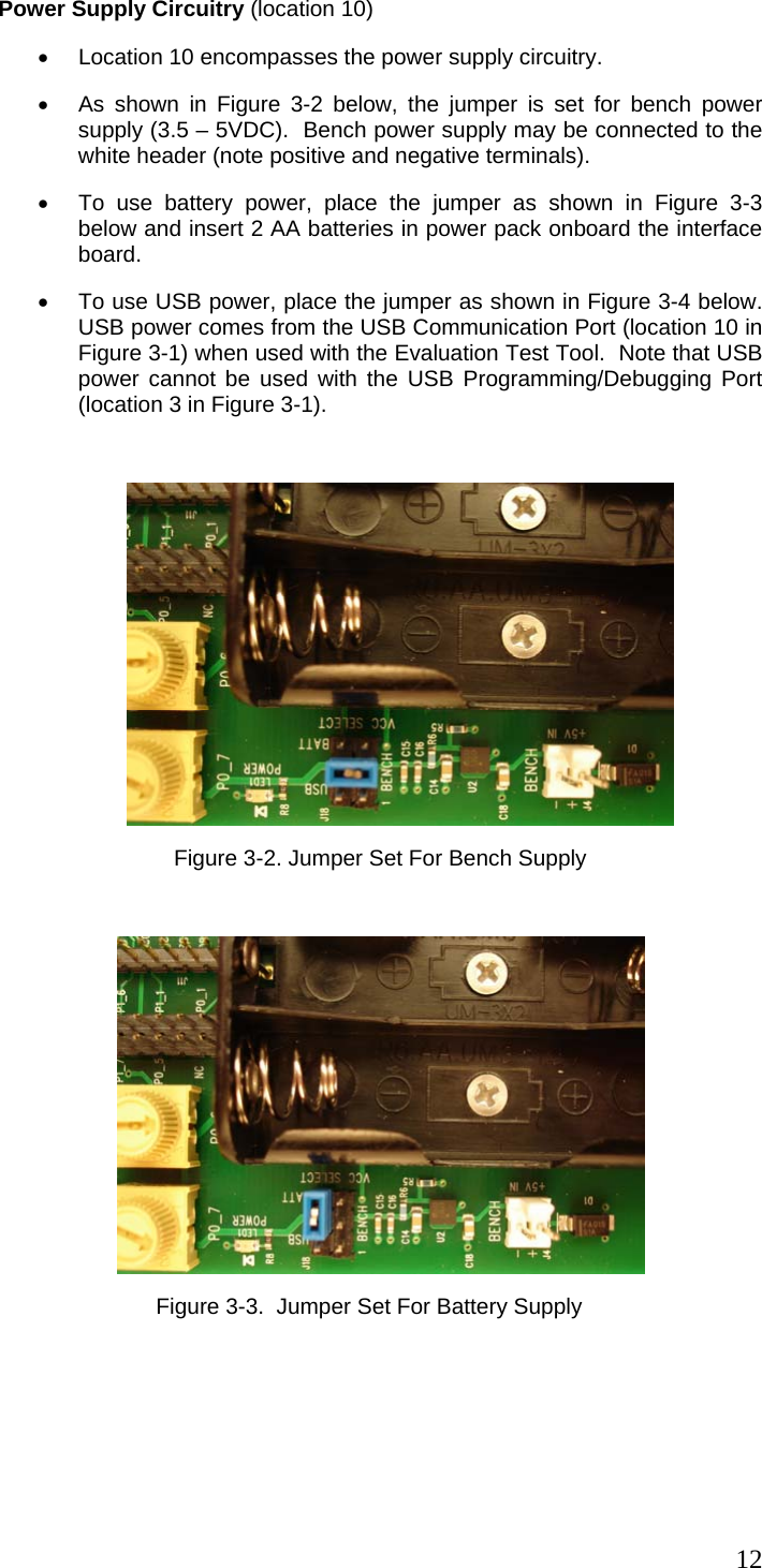
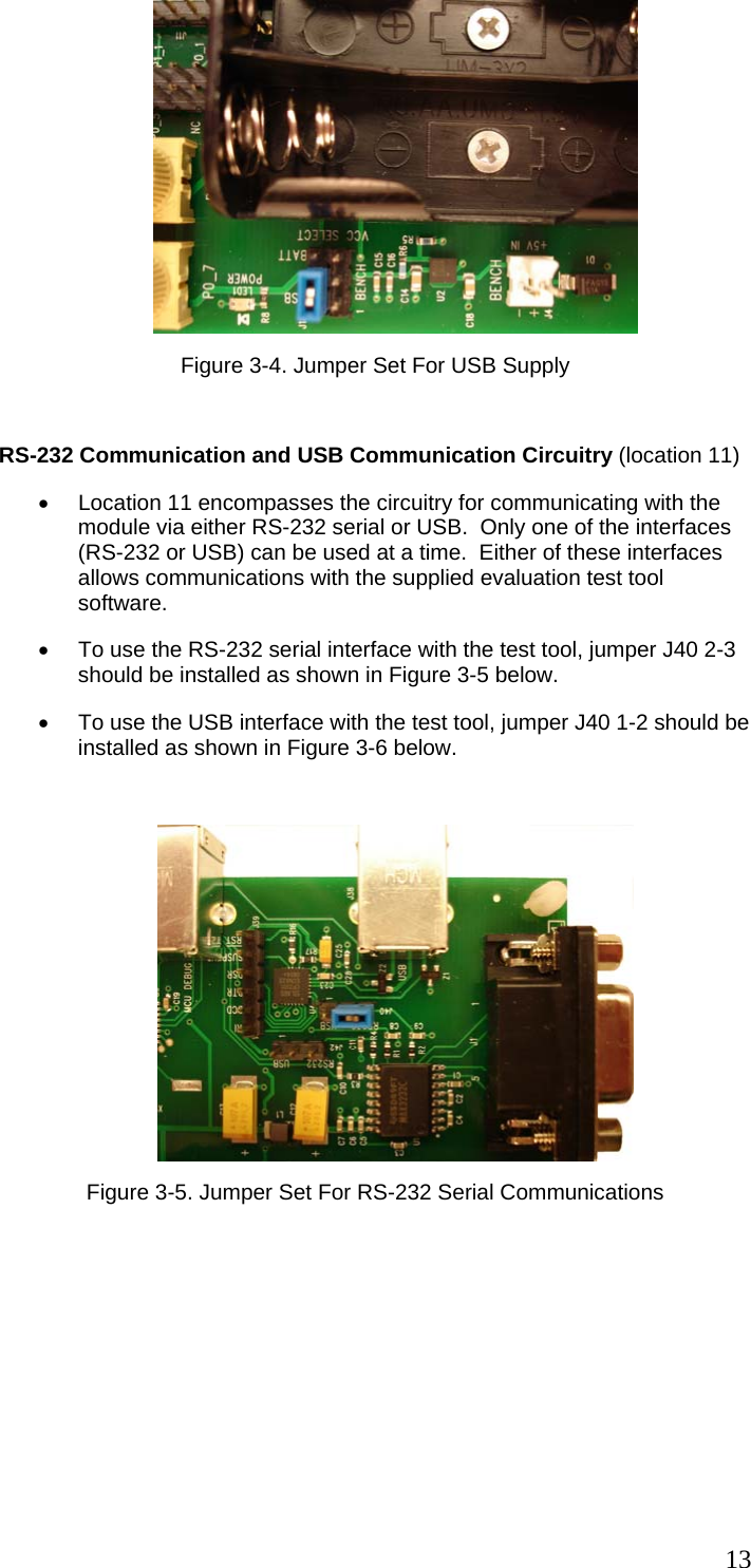
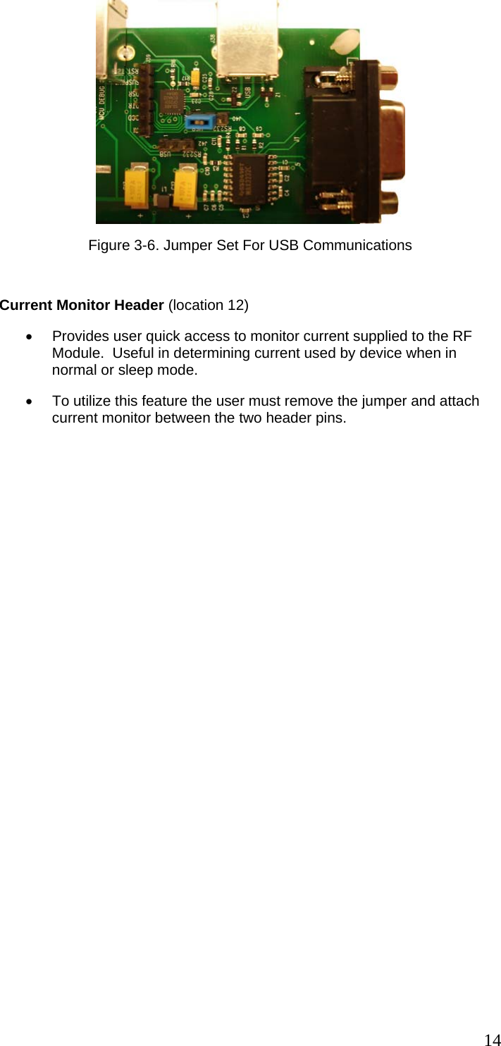
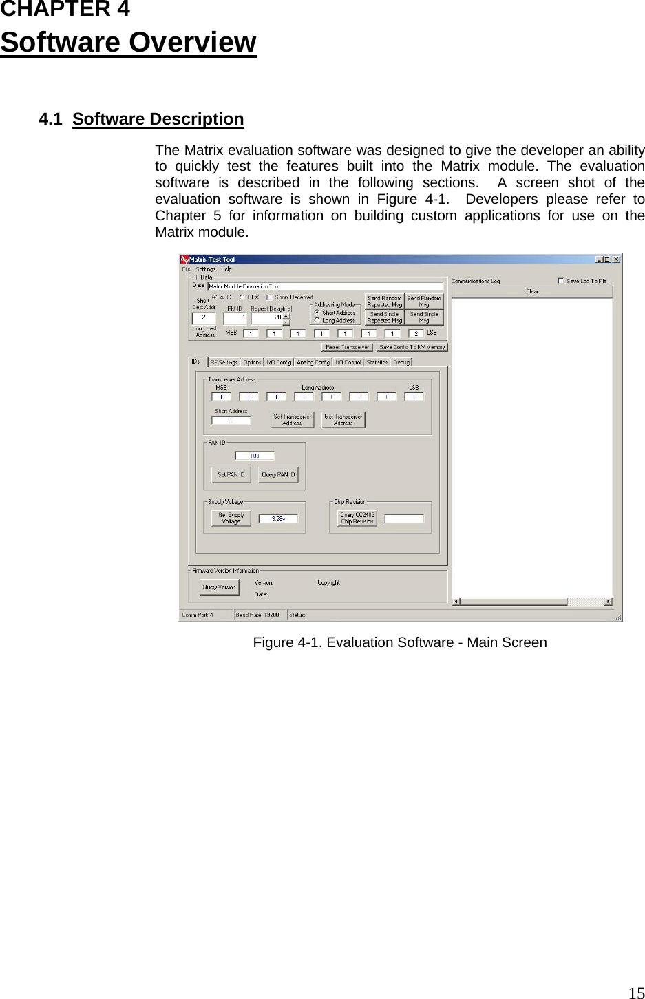
Laird Connectivity MATRIXHP Transceiver Module User Manual Manual
LS Research, LLC Transceiver Module Manual
UserManual.wiki
>
Laird Connectivity
>
MATRIXHP User Manual
Manual
Navigation menu
Upload a User Manual
Namespaces
Wiki Guide
HTML
PDF
Info
Views
User Manual
Discussion / Help
Navigation
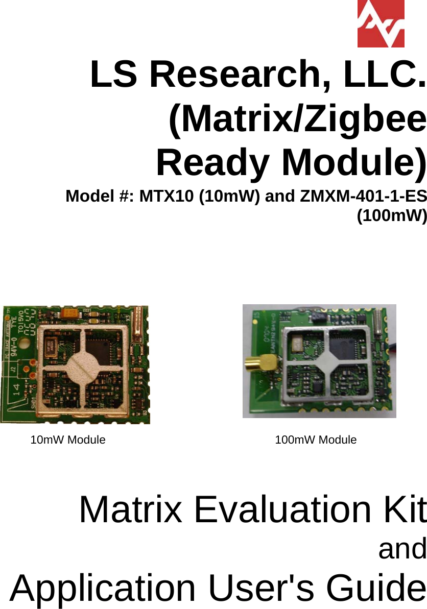
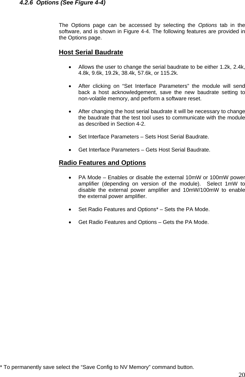
![2 About This Manual This document provides the user with details in setting up and using the Matrix evaluation kits [Part#: MTX10-KIT1 (10mW) and MTX12-KIT1 (100mW)]. The document also provides information and references for software developers to write applications for use with the Matrix modules [Part#: MTX10 (10mW) and ZMXM-401-1-ES (100mW)]. This document contains the following chapters: Chapter 1 – Evaluation Kit Overview Chapter 2 – Quick Start Chapter 3 – Interface Module Description Chapter 4 – Matrix Evaluation Software Chapter 5 – Matrix/Zigbee Ready Module Input/Output Chapter 6 – Matrix Application Guide Appendix A – Open Field Range Test Results Appendix B – Agency Statements Related Documents Host Protocol EICD](https://usermanual.wiki/Laird-Connectivity/MATRIXHP/User-Guide-857875-Page-2.png)