Laird Connectivity MATRIXLP 802.15.4 Transceiver Module User Manual Manual
LS Research, LLC 802.15.4 Transceiver Module Manual
Manual

LS Research, LLC.
(Matrix/Zigbee
Ready Module)
Model #: ZMXM-400-1 (10mW) and MTX12
(100mW)
Matrix Evaluation Kit
and
Application User's Guide
2
About This Manual
This document provides the user with details in setting up and using the
Matrix evaluation kits [Part#: MTX10-KIT1 (10mW) and MTX12-KIT1
(100mW)]. The document also provides information and references for
software developers to write applications for use with the Matrix modules
[Part#: MTX10 (10mW) and MTX12 (100mW)].
This document contains the following chapters:
Chapter 1 – Evaluation Kit Overview
Chapter 2 – Quick Start
Chapter 3 – Interface Module Description
Chapter 4 – Matrix Evaluation Software
Chapter 5 – Matrix/Zigbee Ready Module Input/Output
Chapter 6 – Matrix Application Guide
Appendix A – Open Field Range Test Results
Appendix B – Agency Statements
Related Documents
Host Protocol
EICD

3
Index
CHAPTER 1......................................................................................................................................................... 4
MATRIX EVALUATION KIT OVERVIEW ............................................................................................................... 4
CHAPTER 2......................................................................................................................................................... 5
QUICK START.................................................................................................................................................... 5
CHAPTER 3......................................................................................................................................................... 9
MATRIX INTERFACE MODULE ........................................................................................................................... 9
CHAPTER 4....................................................................................................................................................... 15
SOFTWARE OVERVIEW ................................................................................................................................... 15
CHAPTER 5....................................................................................................................................................... 33
MATRIX/ZIGBEE READY MODULE INPUT/OUTPUT ......................................................................................... 33
CHAPTER 6....................................................................................................................................................... 35
MATRIX APPLICATION GUIDE.......................................................................................................................... 35
APPENDIX A..................................................................................................................................................... 47
RANGE TEST RESULTS................................................................................................................................... 47
APPENDIX B..................................................................................................................................................... 48
AGENCY STATEMENTS ................................................................................................................................... 48

4
CHAPTER 1
Matrix Evaluation Kit Overview
1.1 Description
The evaluation kit provides the end user the ability to quickly become familiar
with the Matrix module. Included in the kit are two Matrix modules and a
quick start guide to demonstrate the communication link between the two
modules. Also included is a GUI interface referred to as the Matrix
Evaluation Test Tool (TT) to quickly communicate with the RF modules.
The Evaluation software demonstration is presented in Chapter 4. The
important features provided by the evaluation software are:
• Short and Long Addressing
• Configurable Digital and Analog I/O
• Demonstrating a Wireless Link
• Packet Error Rate Statistics.
1.2 Contents
The Matrix Evaluation Kit Contains:
Two RF Modules with Firmware Loaded and Soldered to the
Interface Modules
Two Interface Modules
Two RS-232 Interface Cables
4 AA Batteries
1 CD (includes User’s Guide, Host Protocol Document, EICD, and
Matrix Evaluation Tool “Setup.exe” file)
5
CHAPTER 2
Quick Start
2.1 Board Description
The Matrix module is a 2.4GHz 802.15.4 data transceiver module based on
the Chipcon CC2430 Low Power 8051/Transceiver device. It provides
enhanced range performance with either a 10mW or 100mW* power
amplifier. The module also contains an integrated PCB trace antenna.
Power is supplied by the host device through the interface connection in
accordance to the operating voltage requirements with a nominal operating
voltage of +3.3V. Exact details on the interface connections and messaging
are available in the Matrix Electrical Interface Control Drawing.
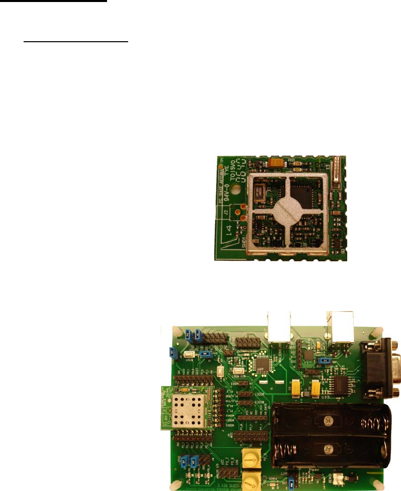
Figure 2-1. Top-Side of RF Matrix Module
Figure 2-2. Top Side of Matrix Interface Board
* Operation is Limited to 10mW Maximum for European Union Compliance
6
2.2 Operational Overview
The quick start demonstration presented in this chapter is referred to as the
ping pong test. The ping pong test allows an end user to easily verify
communication between two transceivers and get a feel for the quality of the
link via feedback of the flashing LEDs.
Operation involves two boards, with one designated as a master device and
the other as a slave device. The master periodically transmits packets to the
slave. If the slave receives and verifies the packet, it will flash its LEDs and
transmit an acknowledgement to the master. If the master receives and
verifies the acknowledgement, it will flash its LEDs.
In normal ping pong mode, LEDs indicate signal strength (two LEDs on
indicate high signal strength, one LED indicates low signal strength). If the
LEDs do not light, the packet or acknowledgement was not received.
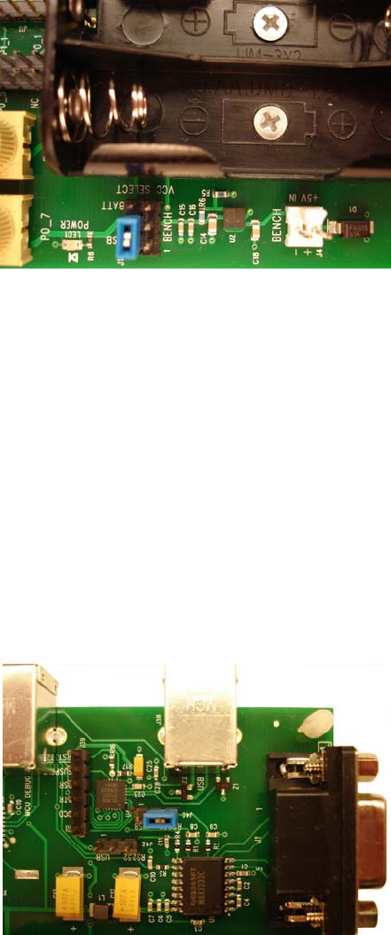
2.2.1 Power Up
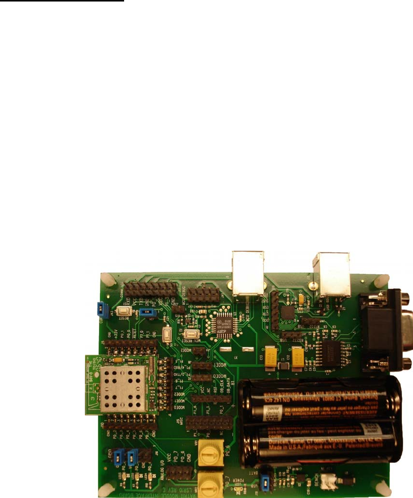
Insert batteries into interface boards and verify that battery supply is selected
using the jumper as shown in Figure 2-3 below (J43 1-2, J18 4-6, J16 5-6,
J16 9-10, and J36 1-2).
Figure 2-3. RF Matrix Module and Interface Board

7
2.2.2 Master/Slave Selection
Master device setup:
1. Press reset button (S1), see Figure 3-1 location 5, and user button
(S3), see Figure 3-1 location 6, on Interface Board simultaneously.
2. Release reset button (S1) on Interface Module.
3. Wait until yellow LED (LED2) is lit, then release reset button (S1).
Slave device setup:
1. Press reset button (S1) and user button (S3) on Interface Board
simultaneously.
2. Release reset button (S1) on Interface Module.
3. Quickly release the user button (S3) (Release within 1.5 seconds of
performing step 2 above).
2.2.3 Association Mode
In association mode, the red LED (LED3) will flash rapidly on each board
until it has linked with the other device. At this point, the red LED (LED3) will
go out and the yellow LED (LED2) will begin to flash rapidly for
approximately two seconds. Association mode lasts up to thirty seconds
after power up, so the master and slave pair should be powered up at
relatively the same time. If the transceivers link, they will enter the ping pong
mode after association mode times out. However, if they do not link, they will
not communicate and the sequence must be repeated from the point of
master/slave selection at power up.
2.2.4 Ping Pong Mode
In ping pong mode, the master and slave boards will flash one or two LEDs
with each packet (slave) or acknowledge (master) received, based on
message signal strength. Refer to Table 2-1 below for a description of the
LEDs versus signal strength. In case there is a lot of traffic on the default
channel, it is possible to change the channel.
Red LED Yellow LED Signal Strength
Off Off None
Off On Marginal
On Off Good
On On Excellent
Table 2-1. LED Signal Strength Definitions
8
2.2.5 Channel Changing (can only be peformed if boards have been associated)
While in the ping pong mode, the current channel can be changed to one of
four other unique channels (four channels total). This is accomplished by
holding the push button for approximately two seconds, at which point the
yellow LED (LED2) will be lit steady. Once the push button is released, the
current channel option number (one through four) is displayed by a series of
flashes on the red LED (LED3). Each short push button press will increment
the channel option number and display it with a given number of flashes on
the red LED (LED3). To accept the last selected channel, hold the push
button until the yellow LED (LED2) goes out (approximately two seconds).
After again releasing the button, the device will return to the ping pong mode.
Note that both the master and slave devices must be set to the same
channel option number for the pair to communicate, and each board must be
individually set to that given channel option number.
9
CHAPTER 3
Matrix Interface Module
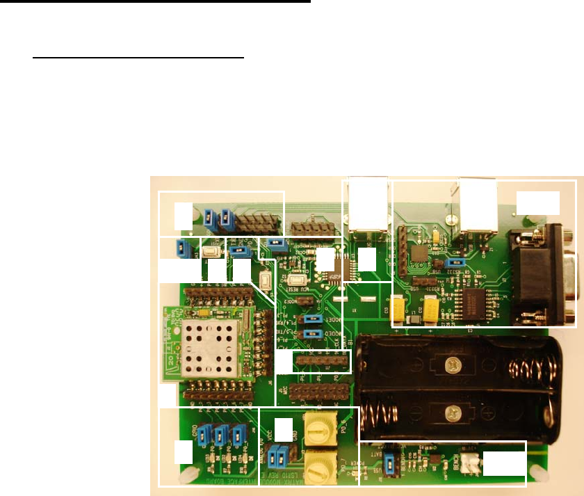
3.1 Interface Module Overview (See Figure 3 – 1 for Photo)
The interface module provides the user the ability to quickly assess the
functions of the Matrix module such as I/O and the mobility to verify
operation of a wireless link in any environment of the user’s choosing.
This chapter describes in detail the functions of the Matrix interface board
that can be verified using the Matrix evaluation software provided in this kit.
Figure 3 -1 Interface Module with Matrix Module Inserted in Socket
3.1.1 Interface Board Description for Each Location Shown in Figure 3-1
Serial Communications Header (location 1)
• Header that allows the user to monitor the serial TX (MODTXD) and
RX (MODTXD) data lines from section 9 as shown in Figure 3-1
above. The header also provides quick access to Port C pins 0 and
1 on the microprocessor.
Mode Select and Programmer/Debugger Jumpers (location 2)
• Leave jumpers uninstalled for normal operation. Jumpers J2 1-2 and
J8 1-2 should be installed in order to program or debug the CC2430
with the USB Programming/Debugging Port.
10
1
8
9
11
1
2
3
5
4
2
7
6
10
Programming/Debugging PC Connector (location 3)
• Location 3 refers to the programming/debugging PC connector. Via
this USB connector it is possible to either program the Matrix Module
or debug when developing custom firmware for the module.
• For programming the Matrix Module with custom firmware, the
suggested programming software tool is the “Chipcon SmartRF04
Flash Programmer”. This tool is available from TI/Chipcon. In
addition to the software tool a USB A-B cable is also required for
connection between the interface board and a PC.
• For debugging firmware that is developed using the IAR Embedded
Workbench for 8051, this USB connector can also be used. Again a
USB A-B cable is required. Additionally the jumpers J2 1-2, J8 1-2,
and J37 1-2, shown in location 2 of Figure 3-1 need to be installed.
Off Board Programming Header (location 4)
• Location 4 refers to the off board programming header. Via this
header it is possible to connect to an off board Matrix Module and
program it while in-circuit.
• A custom cable needs to be built that will allow the off board Matrix
Module to be connected to the interface board. Signals that are
provided on header J11 include “DEBUG_DATA”, “DEBUG_CLK”,
“RST”, “GND”, AND “VCC”.
• Refer to the “Programming/Debugging PC Connector” section above
for information on programming the Matrix Module.
Reset Button (location 5)
• Location 5 indicates the white button that provides ability to reset the
microprocessor on the Matrix module.
User Button (location 6)
• Location 6 indicates the white user button. Its main purpose is for
use with the ping pong range test (described in Section 2.2 above).
In order to use this button jumper J36 1-2 needs to be installed.
Headers for Access to All I/O Pins (location 7)
• Header to provide quick access to all of the I/O pins on the Matrix
Module.
LED Enable/Disable Header (location 8)
• To utilize LED’s the jumpers must be connected as shown in Figure
3-1. The jumpers may be removed to externally access pins P0_2,
P0_3, and P0_4 for input or output operation.
11
Analog Input Select Header (location 9)
• Location 9 shows 2 yellow variable analog potentiometers. With the
jumpers installed as shown in location 9 (at locations J3 3-4 and J3
5-6) on the ANALOG I/O header, the onboard potentiometers may
be utilized to demonstrate the analog capabilities of the Matrix
Module.
• Remove the two jumpers to utilize external analog or digital
peripherals on pins P0_6 and P0_7.
12
Power Supply Circuitry (location 10)
• Location 10 encompasses the power supply circuitry.
• As shown in Figure 3-2 below, the jumper is set for bench power
supply (3.5 – 5VDC). Bench power supply may be connected to the
white header (note positive and negative terminals).
• To use battery power, place the jumper as shown in Figure 3-3
below and insert 2 AA batteries in power pack onboard the interface
board.
• To use USB power, place the jumper as shown in Figure 3-4 below.
USB power comes from the USB Communication Port (location 10 in
Figure 3-1) when used with the Evaluation Test Tool. Note that USB
power cannot be used with the USB Programming/Debugging Port
(location 3 in Figure 3-1).
Figure 3-2. Jumper Set For Bench Supply
Figure 3-3. Jumper Set For Battery Supply
13
Figure 3-4. Jumper Set For USB Supply
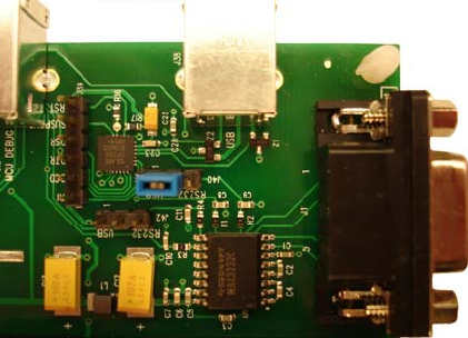
RS-232 Communication and USB Communication Circuitry (location 11)
• Location 11 encompasses the circuitry for communicating with the
module via either RS-232 serial or USB. Only one of the interfaces
(RS-232 or USB) can be used at a time. Either of these interfaces
allows communications with the supplied evaluation test tool
software.
• To use the RS-232 serial interface with the test tool, jumper J40 2-3
should be installed as shown in Figure 3-5 below.
• To use the USB interface with the test tool, jumper J40 1-2 should be
installed as shown in Figure 3-6 below.
Figure 3-5. Jumper Set For RS-232 Serial Communications
14
Figure 3-6. Jumper Set For USB Communications
Current Monitor Header (location 12)
• Provides user quick access to monitor current supplied to the RF
Module. Useful in determining current used by device when in
normal or sleep mode.
• To utilize this feature the user must remove the jumper and attach
current monitor between the two header pins.
15
CHAPTER 4
Software Overview
4.1 Software Description
The Matrix evaluation software was designed to give the developer an ability
to quickly test the features built into the Matrix module. The evaluation
software is described in the following sections. A screen shot of the
evaluation software is shown in Figure 4-1. Developers please refer to
Chapter 5 for information on building custom applications for use on the
Matrix module.
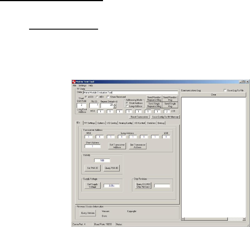
Figure 4-1. Evaluation Software - Main Screen
16
4.2 Software Setup
Prior to installing the test tool, power the Matrix module and connect up
either the RS-232 serial communications or USB communications cable.
Refer to Section 3 above for the correct jumper settings for each the power
supply connection and communications connection that will be used
(Jumpers J17 11-12 and J17 15-16 should be installed, jumper J40 1-2 is for
USB or J40 2-3 is for RS-232, and jumper J18 3-4 is for bench supply, J18 2-
4 is for USB communications supply, or J18 4-6 is for battery supply).
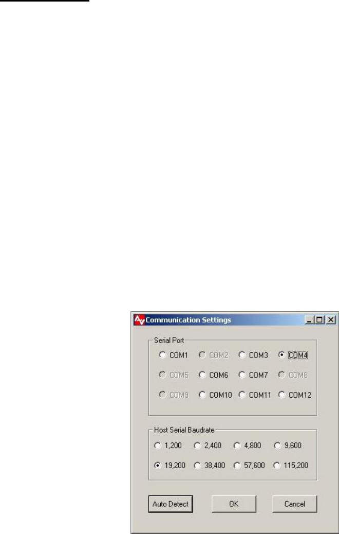
Note that when using the USB communications connector and cable that a
virtual serial COM port is created that should show up in the
“Communications Settings” dialog shown in Figure 4-2 below.
Install the Evaluation test tool using the self extracting setup program and
execute the MatrixTT.exe to start the program.
If the bottom status bar as shown in Figure 4-1 shows a COM port number
and a baudrate, then connection with the module has been successful and
you can skip to Section 4.2.1.
If the bottom status bar shows “Comm Port: None”, then the test tool was not
able to find a Matrix module on any of the available PC COM ports.
Pull down the “Settings” menu and click the “Communications” entry. The
screen shown in Figure 4-2 will appear.
Figure 4-2. Communication Setup Screen under “Settings” Pull Down Menu
The default baudrate is set to 19,200 baud, so leave that setting alone.
Determine serial port in use and select “OK”. Next click the “Get Version”
button on the bottom of the test tool to verify communication with the device.
If the version does not appear, verify correct COM port and select “OK” and
verify communication successful. Another option if the COM port in use is
not known is to select “Auto Detect”. If “Auto Detect” is successful the status
bar should show a comm port number and a baudrate.
If communication is still unsuccessful with the Matrix module, verify all jumper
settings, restart test tool, and perform steps outlined above.

17
4.2.1 Main Section of Test Tool (Upper left portion of the Test Tool as shown
in Figure 4-1)
RF Data
• Data - Text box to allow user to transmit desired messages to other
modules or view messages from another module.
• Ascii/Hex (Radio Buttons) – Gives user ability to view or enter
messages in Hex or Ascii format
• Show Received (Check Box) – If checked the RF Data text box
displays received data in selected format.
• Addressing Mode – Selects whether messages are sent to a long (64
bit) or short (16 bit) address.
• Repeat Delay – Allows user to adjust time between sending repeated
messages.
Reset Transceiver (command button)
• Performs a software reset of the microcontroller.
Save Config to NV Memory (command button)
• Permanently saves configuration settings from IDs, RF Settings, and
Debug tabs to non-volatile memory. This feature allows users to
cycle power or reset the module without losing previously saved
settings.
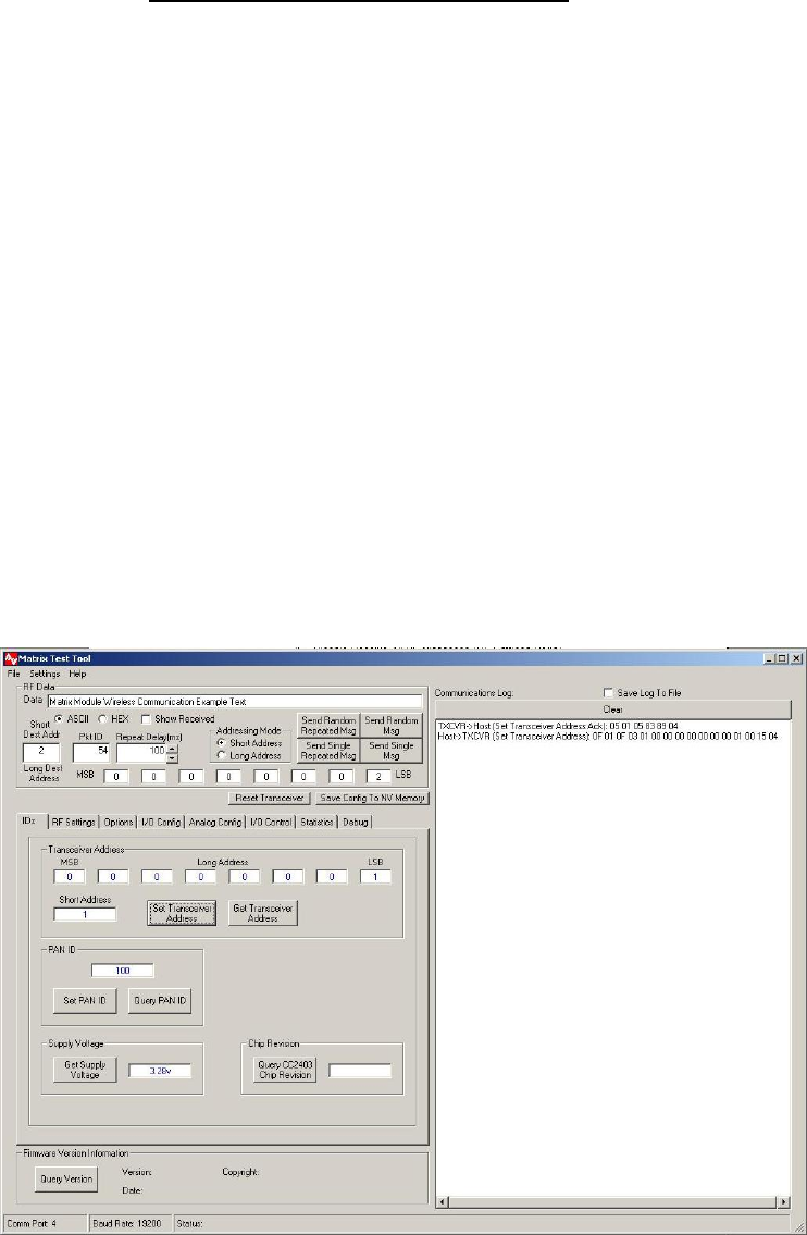
4.2.2 Setting Device Identification (See Figure 4-1)
Transceiver Address
• Short Address – Device defaults to using short address unless this
field is set to 65,534. If using short address protocol only use values
from 0 to 65,533.
• Long Address – Eight byte address used for communication between
devices if short address is set to 65,534.
• Set Transceiver Address – Sets Long and Short Address*
• Get Transceiver Address – Gets Long and Short Address*
PAN ID (Personal Area Network Identification)
• Set PAN ID – Range 0 to 16383 (14 bit Value)
• Get PAN ID – Returns current PAN ID

18
4.2.3 Getting Supply Voltage (See Figure 4-1)
Supply Voltage
• Get Supply Voltage – Gets the voltage that is applied to the Matrix
module.
• The value returned is a single byte. To determine the voltage from
the reading that is returned use the following formula. Supply
Voltage = (Reading / 255) x 3.75
4.2.4 Getting CC2430 Chip Revision (See Figure 4-1)
Chip Revision
• Query CC2430 Chip Revision – Gets the revision number of the
CC2430 RF transceiver. Rev A will be 0x00, Rev B will be 0x01,
Rev C will be 0x02, etc.
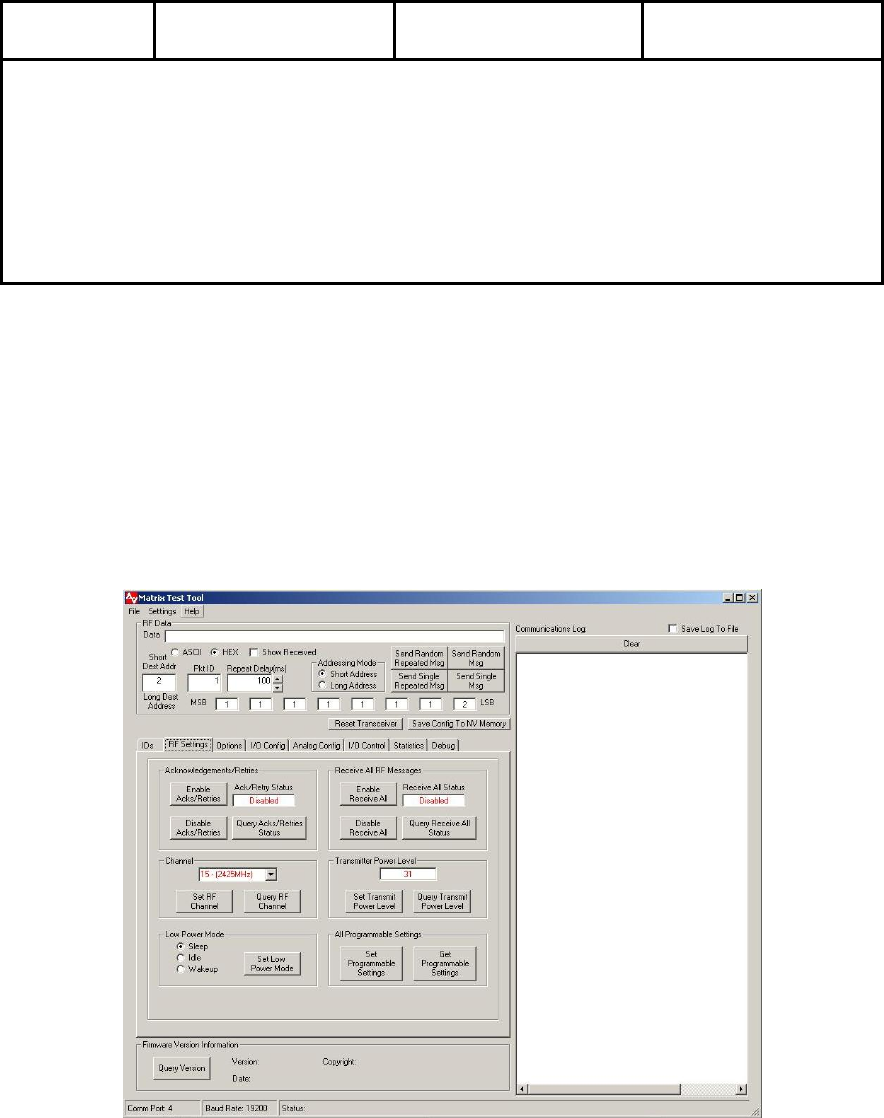
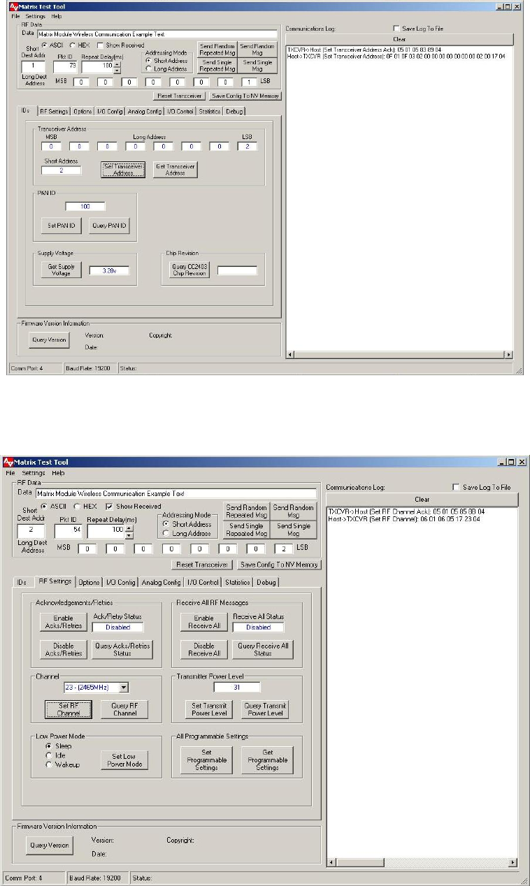
4.2.5 RF Settings (See Figure 4-3)
The RF Settings page can be accessed by selecting the RF Settings tab in
the software and is shown in Figure 4-3. The following features are provided
in the RF settings page.
• Acknowledgement Settings* – If enabled the destination device will
transmit an acknowledgement to the originating device. If disabled
the destination device will not send an acknowledgement back to the
originating device. Query Acknowledgement settings displays current
setting in text box.
• Receive All Messages Setting* - If enabled all messages will be
received from devices with same PAN ID and RF Channel and will
inhibit device from transmitting. This feature is only to be used for
diagnostic purposes (Feature Currently Not Available)
• Set or Query RF Channel* - channels 11 (2405MHz) – 26
(2480MHz) may be used
• Set or Query Transmitter Power Level* - Ranges from 0 – 31 (31 is
max level). Refer to Table 4-1 for information on power setting
versus conducted output power level.
• Set RF Module Power Mode for Sleep, Idle, or Wakeup.
• Set/Get All Programmable Settings (PAN ID, Txcvr Long Address,
Txcvr Short Address, RF Channel, Receive All Setting (Feature Not
Available), RF Acks/Retries, RF Power Level).
* To permanently save select the “Save Config to NV Memory” command button.
19
RF Power
Level Setting Module Output Power
Without PA Module Output Power
With 10mW PA Module Output Power
With 100mW PA
0-6 -25dBm -14.5dBm 1.5dBm
7-16 -15dBm -5dBm 11dBm
17-21 -10dBm 0dBm 15dBm
22-24 -7dBm 3dBm 17dBm
25-26 -5dBm 5.5dBm 18dBm
27-28 -3dBm 7.5dBm 18.5dBm
29-30 -1dBm 9dBm 19dBm
31 0dBm 10dBm 20dBm
Table 4-1. RF Power Level
Figure 4-3. RF Settings

20
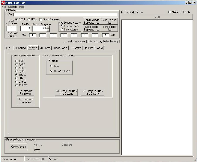
4.2.6 Options (See Figure 4-4)
The Options page can be accessed by selecting the Options tab in the
software, and is shown in Figure 4-4. The following features are provided in
the Options page.
Host Serial Baudrate
• Allows the user to change the serial baudrate to be either 1.2k, 2.4k,
4.8k, 9.6k, 19.2k, 38.4k, 57.6k, or 115.2k.
• After clicking on “Set Interface Parameters” the module will send
back a host acknowledgement, save the new baudrate setting to
non-volatile memory, and perform a software reset.
• After changing the host serial baudrate it will be necessary to change
the baudrate that the test tool uses to communicate with the module
as described in Section 4-2.
• Set Interface Parameters – Sets Host Serial Baudrate.
• Get Interface Parameters – Gets Host Serial Baudrate.
Radio Features and Options
• PA Mode – Enables or disable the external 10mW or 100mW power
amplifier (depending on version of the module). Select 1mW to
disable the external power amplifier and 10mW/100mW to enable
the external power amplifier.
• Set Radio Features and Options* – Sets the PA Mode.
• Get Radio Features and Options – Gets the PA Mode.
* To permanently save select the “Save Config to NV Memory” command button.
21
Figure 4-4. Options
22
4.2.7 I/O Configuration (See Figure 4-5)
The I/O Configuration page can be accessed by clicking the I/O Config tab in
the software, and is shown in Figure 4-5. The I/O Configuration page can be
used to configure select I/O pins for digital or analog operation. Refer to
Table 4-2 for information on the I/O pin capabilities.
Figure 4-5. Digital I/O Configuration
I/O Configuration
• Initial Output Level or Input Setup – Gives user the ability to set
selective port pins for Output (0 or 1 Initial Value), Predefined LED
Functionality (L), Analog Input (A), or Input with or without internal
pull-up or pull-down resistor enabled.
• Sleep Output Level or Input Setup - Gives user the ability to
configure I/O pin states as desired for sleep operation. If Unchanged
(U) is selected then the particular pin(s) retain their state when sleep
operation is selected.

23
Pin Available
To User Analog
Input LED
Function Output Input Pull-up
Pull-down Notes
P0_0 X X X X X X
If LED functionality is enabled on this pin,
then the functionality is automatically
disabled from pin P0_2 and P0_3.
P0_1 X X X X X X
If LED functionality is enabled on this pin,
then the functionality is automatically
disabled from pin P0_2 and P0_3.
P0_2 X X X X X X
If LED functionality is enabled on this pin,
then the functionality is automatically
disabled from pin P0_0 and P0_1.
P0_3 X X X X X X
If LED functionality is enabled on this pin,
then the functionality is automatically
disabled from pin P0_0 and P0_1.
P0_4 X X X X X
P0_5 X X X X X
P0_6 X X X X X
P0_7 X X X X X
P1_0 X X X
P1_1 X X X
P1_2 X X X
Used internally to enable/disable external
power amplifier (output).
P1_3 X X X
Host interface Clear-To-Send (CTS) serial
handshake signal (output).
P1_4 X X X
Host interface serial receive data signal
(input).
P1_5 X X X
Host interface serial transmit data signal
(output).
P1_6 X X X X
P1_7 X X X X
Table 4-2. I/O Pin Capabilities
24
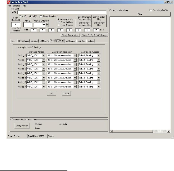
4.2.8 Analog Configuration (See Figure 4-6)
The Analog Configuration page can be accessed by clicking the Analog
Config tab in the software, and is shown in Figure 4-6. The Analog
Configuration page can be used to configure the pins set as analog inputs
(Refer to Section 4.2.7) for their analog-to-digital converter settings.
Figure 4-6. Analog Input Configuration
Analog Input ADC Settings
• Reference Voltage – Gives user the ability to select the voltage
reference that will be used for the conversion. Options consist of the
AVDD_SOC supply voltage, the internal 1.25v reference, a voltage
applied to analog input pin 7 (P0_7), or the differential voltage
applied between analog input pins 6 and 7 (P0_6 and P0_7).
• Conversion Resolution - Gives user the ability to select the resolution
of the conversion. Options consist of 8, 10, 12 or 14 bits of
resolution, and the conversion takes longer as the resolution of the
conversion increases.
• Readings To Average – Gives user the ability to select the number of
ADC converter readings to average before returning a result.
Options consist of 1, 2, or 4 readings to average.
25
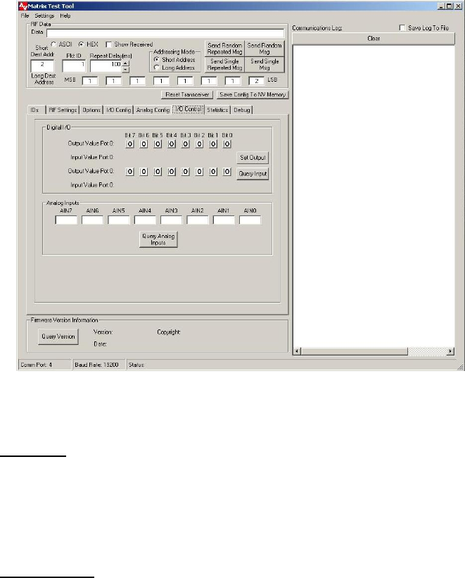
4.2.9 I/O Control (See Figure 4-7)
The I/O Control page can be accessed by clicking the I/O Control tab in the
software, and is shown in Figure 4-7. The I/O Control page can be used to
read analog and digital inputs and set digital outputs.
Figure 4-7. I/O Control
Digital I/O
• Set Output – Sets pins configured as digital outputs to the selected
level (0 or 1).
• Query Input – Gets the input level (0 or 1) for pins configured as
digital inputs.
Analog Inputs
• Readings – Displays analog input values read by the microcontroller
for pins configured as analog inputs. The analog readings are taken
using the settings in the Analog Config tab (Section 4.2.8).
26
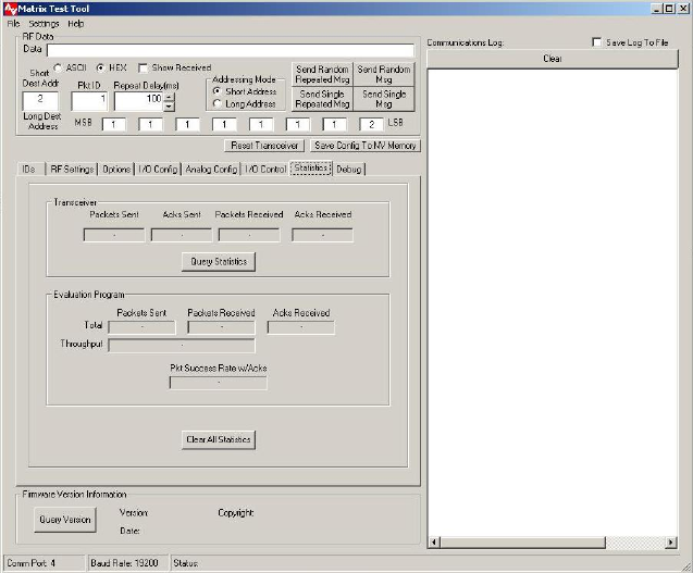
4.2.10 Statistics (See Figure 4-8)
The Statistics page can be accessed by clicking the Statistics tab in the
software, and is shown in Figure 4-8. The Statistics page can be used to
evaluate the wireless link for packet error rates and throughput.
Figure 4-8. Statistics Screen
27
“Transceiver” Statistics
• Packets Sent - Number of packets transmitted.
• Acknowledgements (Acks) Sent – Number of acknowledgements
sent by receiver.
• Packets Received – Number of packets received.
• Acks Received – Number of acknowledgements received by the
transmitter.
“Evaluation Program” Statistics
The window toward the bottom the page labeled “Evaluation
Program” contains information about the integrity of the link between
the host computer and the radio board.
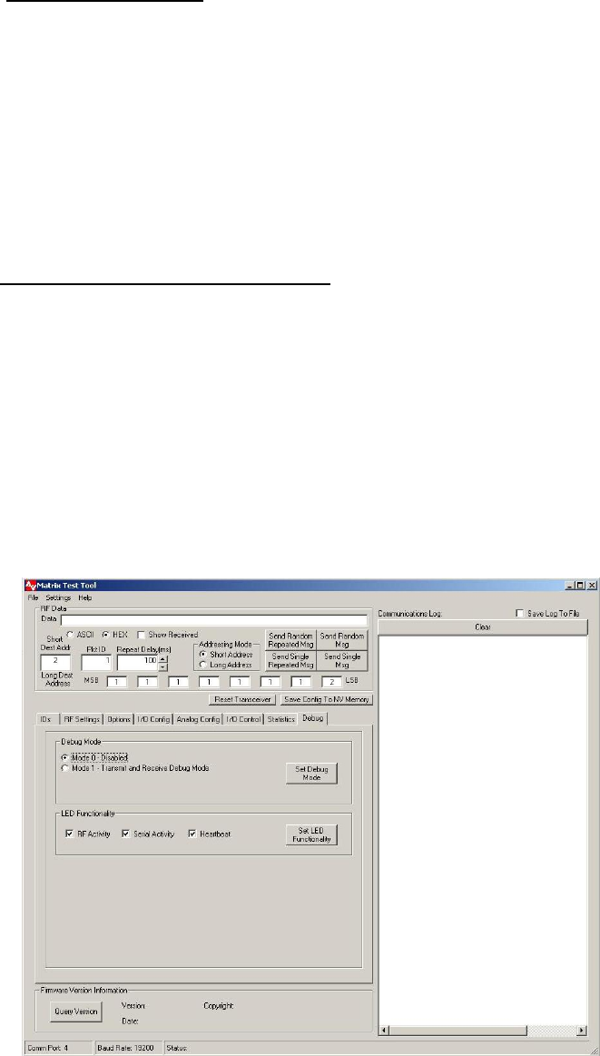
4.2.11 Debug Settings (See Figure 4-9)
The Debug Settings page can be accessed by clicking the Debug tab in the
software, and is shown in Figure 4-9. The Debug page can be used to
enable debug signals and internal LED functionality.
Figure 4-9. Debug Settings Screen

28
Debug Mode
• Mode 0 – No debug pulses on pins.
• Mode 1 – Refer to Host Protocol Document for Information.
LED Functionality (Refer to Host Protocol Document for Information)
• Depending on the I/O Configuration for the pins that can have LED
outputs enabled (refer to Section 4.2.7), and whether or not the
specific LED functionality is enabled, the LEDs will momentarily flash
when serial activity, RF activity, or heartbeat activity occurs.
• Refer to Table 4.3 below for information on which output pin, and
corresponding LED if populated on the module or interface board,
will pulse based on the activity.
• RF Activity – LED flashes when transmitting or receiving a RF
message.
• Serial Activity – LED flashes when communicating through the serial
port. Received RF messages will flash the transmit LED if the
message is transmitted out the host serial port.
• Heartbeat – LED flashes every two seconds to visually verify to user
that device is operating.
Pins Configured
For LED Functionality
RF Rx
RF Tx
Serial Rx
Serial Tx
Heartbeat
Onboard LEDs
P0_0 - Green
P0_1 - Red
Red (P0_1)
Green (P0_0)
Red (P0_1)
Green (P0_0)
Green (P0_0)
Interface Board LEDs
P0_2 - Red
P0_3 - Yellow
Red (P0_2)
Yellow (P0_3)
Red (P0_2)
Yellow (P0_3)
Yellow (P0_3)
Table 4-3. LED Functionality

29
4.3 Setting Up and testing a Wireless Link
Operational testing of the Matrix RF module requires at least 2 units in order
to establish a link. One unit will be the initiator and the other will be the
responder. In order for a link to be established it is necessary to setup the
transceiver’s RF Channel, long or short address, and PAN ID.
Link testing may be performed in either a single ended or a round trip
fashion. This can help to differentiate between real world packet error
performance and raw radio performance. If Acknowledgement settings are
not used then it is a single-ended test, if Acknowledgements are enabled
then it is a round trip test.
4.3.1 Single-ended Test
Single ended performance will require 2 computers, since it will be necessary
to read the statistics from each radio. An example setup is outlined below.
Device 1 (Refer to Figures 4-10 and 4-12)
1. Set PAN ID to 100 (IDs Page).
2. Set Short Address to 1 (IDs Page). Note to use long addressing set
short address to 65,535.
3. Disable Acknowledgements/Retries (RF Settings Page).
4. Disable Receive All RF Messages (RF Settings Page).
5. Set to RF Channel 23 (RF Settings Page).
6. Set transmitter power setting to 31 (RF Settings Page).
7. Set Short Destination address to 2 (Located Upper left corner of TT).
8. Select Short Address Radio Button (Upper Section of TT).
*Long may be selected if sending to a long address device.
9. Select “Save Config To NV Memory” Command Button (Upper
Section of TT).
10. Check the Show Received box (Upper Section of Test Tool).
30
Device 2 (Refer to Figures 4-11 and 4-12)
1. Set PAN ID to 100 (IDs Page).
2. Set short address to 2 (IDs Page). Note to use long addressing set
short address to 65,535.
3. Disable Acknowledgements/Retries (RF Settings Page).
4. Disable Receive All RF Messages (RF Settings Page).
5. Set to RF Channel 23 (RF Settings Page).
6. Set transmitter power setting to 31 (RF Settings Page).
7. Set Short Destination address to 1 (Located Upper left corner of TT).
8. Select Short Address Radio Button (Upper Section of TT).
*Long may be selected if sending to a long address device.
9. Select “Save Config To NV Memory” Command Button (Upper
section of TT).
10. Check the Show Received box (Upper Section of Test Tool).
Figure 4-10. ID Settings for Device 1
31
Figure 4-11. ID Settings for Device 2.
Figure 4-12. RF Settings for Initiating and Receiving Device

32
Operational Description
Place the 2 units in physically separate locations and apply power to them.
The statistics will clear when power is cycled, but they will need to be cleared
manually after each test if power is not cycled.
Connect each individual PC serial port to each of the units and verify the
correct destination address is typed in the address field on the top of the test
tool. Type a short message into the “RF Data” window of the initiating
device. The message can be any text or numbers. If no message is entered
it will not be possible to transmit.
Set the “Repeat Delay” to 100 msec if it isn’t already set. Click the “Send
Single Repeated Msg” button to start transmission. The radio will send
messages repeatedly with 100mSec in between messages until the “Stop
Repeat” button is clicked.
Allow the test to run for some convenient amount of time and then stop
transmission. Go to the “Statistics” screen of the initiating device and select
the “Query Statistics” command button and record the packets sent in the
Transceiver section of the test tool. Next select “Query Statistics” on the
receive device and record packets received in the Transceiver section of the
Statistics page. Link success is simply the ratio of the “Packets Received” to
the “Packets Sent”.
This test will give the raw performance of the link in one direction without
retries. It is a good indicator of the RF environment in which the radios are
being used. High levels of noise or other products operating in the 2.4 GHz
band can cause lower packet success rates.
4.3.2 Round Trip Test
To test the ability of the system to retry messages in a noisy environment, it
is necessary to use a round trip test where the remote end can acknowledge
receipt of packets. Use the setup screen as shown in Figure 4-10 thru 4-12
for each respective device, but enable acknowledgements on both devices
(Refer to RF Settings Page).
Perform the test in the same manner as the single ended test. Run enough
transmissions to get a statistically valid sampling of the radio environment
over a reasonable period of time.
Look at the “Statistics” screen on the initiating radio to find the total number
of packets sent. Link quality is displayed in the Pkt Success Rate w/Acks
text box. Total link success is the ratio of “Acks Received” to “Packets
Sent”.

33
CHAPTER 5
Matrix/Zigbee Ready Module Input/Output
5.1 Overview
There are a total of 12 user input/output pins on the Matrix module, all of
which can be configured as digital inputs or outputs. Of the 12 configurable
digital I/O pins, 8 of them can also be configured as analog inputs.
5.2 Digital Inputs/Outputs
There are 12 configurable digital input/output pins that can be programmed
to be either inputs or outputs. In addition, if the pins are inputs, all except for
two (P1_0 and P1_1) of them can be enabled for either an internal pull-up or
pull-down resistor. Refer to Table 4-2 for the specific I/O pin capabilities.
Using the digital input output pins consists of the following:
Configuring the pins
Select direction (digital input or digital output), enable or disable pull-
up or pull-down resistors for pins configured as digital inputs, and set
the initial output value for pins configured as digital outputs (0 or 1).
These parameters define the configuration of the pins when a reset
occurs. Also the direction and pull-up/pull-down parameters are
used to set the state of the pins after exiting sleep mode. Note that if
the internal pull-up or pull-down resistors are used that all pins within
the same port have to either be pull-ups or pull-downs.
Configuring the sleep state of the pins
Select direction (input or output), enable or disable pull-up or pull-
down resistors for pins configured as digital inputs, and set the
output value for pins configured as digital outputs. Although these
parameters are the same as those shown in the “Configuring the
pins” item shown above, they are independent and are the state of
the pins when the Matrix module is put into Sleep Mode.
Reading the state of the pins configured as inputs
Read the digital value (0 or 1) of the signal applied to the pins
configured as inputs.
Setting the state of the pins configured as outputs
Set the digital value (0 or 1) for the pins configured as outputs.

34
5.3 Analog Inputs
There are 8 pins that can be configured as analog inputs. Refer to Table 4-2
for the specific I/O pin capabilities.
Using the analog input pins consists of the following:
Configuring the pins
Select direction as analog input. Select the analog-to-digital
converter settings for each specific pin configured as an analog input
(refer to Section 4.2.7).
Configuring the sleep state of the pins
Select direction (input or output), enable or disable pull-up or pull-
down resistors for pins configured as digital inputs, and set the
output value for pins configured as digital outputs. Note that pins
configured as analog inputs under normal operating mode can be set
as anything when the Matrix module is put into Sleep Mode.
Reading the state of the pins configured as analog inputs
Read the analog digital value (0 or 1) of the signal applied to the pins
configured as inputs.

35
CHAPTER 6
Matrix Application Guide
6.1 Overview
This Chapter describes the essentials for using the host protocol to configure
and use a Matrix module in an application. Please refer to Host Protocol
Document for Further Details on messaging.
6.1.1 Host Protocol
The host protocol that is used to communicate with a Matrix module is a
simple binary based protocol. Every message in the protocol consists of a
header, a trailer, and potentially some payload information, which is
consistent with other LSR module data packet structures. With the Matrix
module it is possible to configure the baudrate from 1.2k up to 115.2, and as
such it uses a DMA peripheral in conjunction with the UART so that reliable
data transfers are possible at the higher data rate. In order to simplify
operation of the DMA peripheral when used with the UART, all messages
sent to and received from the Matrix module should additionally have the
“Length” byte repeated as the first byte in a packet (prior to the header).
The header is made up of a start byte (0x01), a length byte that is the length
of the entire message including header and trailer, and a message type that
identifies the intention of the message.
The payload varies from message to message but in general includes things
such as data to be sent or received, or configuration information.
The trailer is made up of a checksum, which the sum of all of the bytes in the
message, starting at the start byte (0x01) and up through the payload, and
an end byte (0x04). Note that the checksum computation does not include
the additional “Length” byte that precedes the start byte.
Every message that the host device sends to the Matrix module has a
complimentary acknowledgement message that will get sent back upon
successful decoding and processing by the Matrix module.
6.1.2 Configuration
After power-up or after receiving a “Reset Request” (type 0x18) message,
the Matrix module will read the configurable parameters from the on-board
microcontroller’s non-volatile FLASH memory, and store them in RAM to be
used from that point on. Changing a parameter by sending the module a
new message does not automatically result in the module saving the
parameter to non-volatile memory, but rather just changes the value stored in
RAM. This allows a particular host application to change the configurable
parameters dynamically without unnecessarily writing to, and shortening the
lifetime of, the non-volatile memory. All of the Matrix module’s configurable
parameters that are stored in RAM can be saved to non-volatile memory by
sending a “Save Configuration Values to Non-Volatile Memory” (type 0x11)
message.

36
Communication Parameters
There are six configuration parameters used to setup the Matrix module for
communications, which are outline below.
1. Set PAN ID – The Personal Area Network (PAN) ID is used to
establish networks of transceivers. Only devices with the same PAN
ID will communicate with one another.
2. Set Transceiver Address – The Transceiver Address is used to
differentiate transceivers within a network. Each transceiver should
be configured with a different address. The Transceiver Address
consists of both a short two byte and a long eight byte address.
Setting the short address to 65,534 (0xFFFE) will cause the Matrix
module to use its long address. To use the short address, the short
address should be set to between 0-65,533.
3. Set RF Channel – The RF channel is used to select the channel in
the 2.4GHz band that the transceiver will operate on.
Communication between transceivers is only possible if the devices
are both using the same RF channel. Valid RF channels are from 11
(2405MHz) to 26 (2480MHz).
4. Enable/Disable Receive All RF Messages (Feature Currently Not
Available) – Enabling receive all RF messages allows all messages
on the configured PAN ID to be received by the Matrix module. This
intended use of receive all messages is for diagnostics tools so that
it is possible to see all messages on a network. Note that when this
mode is enabled that it is not possible to transmit RF messages.
5. Enable/Disable RF Acknowledgements and Retries – When RF
Acknowledgements and Retries are enabled, the destination
transceiver will respond to the received RF message with an RF
acknowledgement. If the source transceiver does not receive an RF
acknowledgement, it will attempt to re-send the message to the
destination transceiver up to 3 more times (3 retries). By using
acknowledgments and retries, the likelihood of successfully getting a
message from one transceiver to another increases.
6. Set Transmit Power Level – This setting allows for adjusting the
transmit power, which affects the overall range. The range varies
from 0 to 31.
Input/Output Parameters
There are three configuration messages used to setup parameters for
controlling the user input and output pins, which are outlined below.
1. Set I/O Configuration – This message is used to configure the
direction (input or output), whether or not the internal pull-up or pull-
down resistors are enabled for pins configured as inputs, and the
initial output value for pins configured as outputs. The initial output
value is the default state that output pins will be assigned after
power-up or a “Reset Request” command is issued to the module.

37
2. Set I/O Sleep State – This message defines the state that the I/O
pins will be put into when the low power sleep mode of operation is
requested for the module. Similar to the “Set I/O Configuration”
message, the direction of the pin, whether or not the pull-up or pull-
down resistors are enabled for input pins, and the output value for
output pins can be configured. Upon exiting sleep mode the pins will
be configured back to the state they were in prior to entering sleep
mode.
3. Set Analog Input ADC Settings – This message is used to set up
how the ADC conversion will be done for pins configured as analog
inputs. The settings include the reference voltage that the
conversion is based on, the resolution of the ADC conversion, and
the number of samples to average when a reading is taken. Note
that the higher the ADC conversion resolution the longer it takes to
do a conversion.

38
Diagnostics and Feedback Parameters
There are two configuration parameters used to setup diagnostics and user
LED feedback which are outlined below.
1. Set Debug Mode – Setting the debug mode allows the host
application to configure what debug information gets displayed on
the three mode pins when the mode pins are in their default state.
The default state for the mode pins is that none of the pins are
externally pulled-down. The intent of the debug signals is to allow for
monitoring on an oscilloscope how the device is operating.
2. Set LED Functionality – This message is used to configure if any
LED feedback information is enabled or not, and if it is enabled what
it represents. For modules that are embedded in an enclosure, the
LED functionality can altogether be disabled to further reduce power
consumption. Several examples of the types of functionality that can
be displayed on the LEDs are a heartbeat LED flash to indicate the
microcontroller is running or flashes when an RF or serial message
is either transmitted or received. Multiple functions can be enabled
simultaneously. The LED functionality can be enabled on pins P0_0
and P0_1 or on P0_2 and P0_3, or it can be disabled altogether and
then the pins can be used as user I/O. If LED functionality is
enabled for use on P0_0 and P0_1, either LEDs can be populated on
the Matrix modules itself, or off board LEDs can be utilized. When
LED functionality is enabled for use on P0_2 and P0_2, then it is
required that off board LEDs be used.
Example configuration
The following example will show details of what host protocol messages a
host device would send to a Matrix module to configure all of its
programmable settings. After all of the settings have been sent to the
transceiver, save configuration parameters message is issued to save the
settings to non-volatile memory.
Settings
PAN ID: 100
Transceiver Address: Long Address = 500
(short address needs to be 65,535)
RF Channel: 18
Receive All: Disabled
Acknowledgements and Retries: Enabled
Transmit Power Level: 31 (maximum)
I/O Pin Configuration: All inputs with pull-up resistors
enabled
I/O Pin Sleep State: All inputs with pull-up resistors
enabled (unchanged)
Debug Mode: Disabled
LED Functionality: Heartbeat and flash on RF activity,
LED activity on pins P0_0 and P0_1

39
Host Messages
1. Set PAN ID
< 0x07 0x01 0x07 0x01 0x64 0x00 0x6D 0x04 >
2. Set Transceiver Address
< 0x0F 0x01 0x0F 0x03 0xF4 0x01 0x00 0x00 0x00 0x00 0x00 0x00
0xFF 0xFF 0x06 0x04>
3. Set RF Channel
< 0x06 0x01 0x06 0x05 0x12 0x1E 0x04 >
4. Disable Receive All RF Messages
< 0x06 0x01 0x06 0x07 0x00 0x0E 0x04 >
5. Enable Acknowledgements and Retries
< 0x06 0x01 0x06 0x09 0x01 0x11 0x04 >
6. Set Transmit Power Level
< 0x06 0x01 0x06 0x0F 0x1F 0x35 0x04 >
7. Set I/O Pin Configuration
< 0x0F 0x01 0x0F 0x01E 0x00 0xFC 0x00 0x00 0x00 0x03 0x00
0xFC 0x00 0x00 0x29 0x04 >
8. Set I/O Pin Sleep State
< 0x10 0x01 0x10 0x23 0x00 0x00 0x00 0x00 0x00 0x00 0x00 0x00
0x00 0x00 0x00 0x34 0x04 >
9. Disable Debug Mode
< 0x06 0x01 0x06 0x27 0x00 0x2E 0x04 >
10. Enable Heartbeat and Flash On RF Activity LED Functionality
< 0x06 0x01 0x06 0x28 0x05 0x34 0x04 >
11. Save Configuration Parameters To Non-Volatile Memory
< 0x05 0x01 0x05 0x11 0x17 0x04 >
For all of the messages shown above that would get sent from the host
application to the Matrix module, a host level acknowledgement will be sent
back when it has been successfully processed. It is recommended that the
host application send a message to the module and then wait for an
acknowledgement response prior to sending the next message. This will
take care of flow control and prevent the host application from overflowing
the module.

40
6.1.3 RF Messaging
Overview
The Matrix module provides a versatile command set for communications
between modules. Depending on the application’s requirements, either short
or long address modes can be used. Short addressing mode uses a two
byte transceiver address, while long addressing mode uses eight byte
transceiver addresses. It is also possible to communicate between
transceivers using mixed addressing modes, hence a message can be sent
from a transceiver with a short address to another transceiver with a long
address or vice versa.
There is a single host message that is used to send data from one
transceiver to another and two host messages that are generated when a
message is received. When in receive all (Feature Not Available) mode of
operation and a message is received by a transceiver, host message type
0xA9 is generated and sent out the serial port to the host. In the default
mode of operation (receive all mode disabled) host message type 0x95 is
generated and sent out the serial port to the host.
RF host messages consist of a standard header (start, length and type), RF
message header, payload, and a standard trailer (checksum and stop). The
RF message header contains a Packet ID, a Target/Sender identifier, an
Address Mode byte, and the Transceiver Addresses. The Packet ID is used
to identify each message and should be incremented for each new packet
when sending a message. The Target/Sender byte indicates where the
message originated from and is being sent to. Messages either are
originated from or sent to either the host or the application. The application
is the user application code that is running on the Matrix module (currently
not supported). The host is the host application. The Address Mode byte
describes the type of addressing for the particular message. The upper
nibble indicates the addressing mode used for the destination of the
message, while the lower nibble indicates the mode for the source of the
message. A 0 is used to represent a short address, while a 1 represents a
long address. Following the Addressing Mode is the destination address and
then the source address (for received messages only – types 0x95 and
0xA9).
Short Addressing
In order to use short addressing it is required that the transceiver address be
set between 0 and 65,533 (0xFFFD). Setting the short address to 65,534
(0xFFFE) causes the transceiver module to use the eight byte long address.
Long Addressing
Long addressing mode is configured by setting the short address to 65,534
and then selecting a long address in the range of 0 to
18,446,744,073,709,551,614 (0xFFFFFFFFFFFFFFFE).
Broadcasts
It is possible to broadcast a message to all transceivers configured to the
same RF channel and PAN ID. Messages are broadcast by sending the
message to the short destination transceiver address 65,535 (0xFFFF).

41
Receive All (Feature Currently Not Available)
Receive all mode is used as a diagnostic mode in which a transceiver can
listen to and receive all of the messages from any device that is
communicating on the same PAN ID and RF channel. Messages with long
and short addressing types will be received, and when a message is
received it is sent out the host serial port with a message type of 0xA9. In
receive all mode it is not possible to transmit messages to other transceivers.
Addressing Modes Summary
The Table 6-1 below gives an overview of the addressing modes that are
available in the Matrix module. The table shows a summary of what happens
when messages are sent between two modules (Transceiver A and
Transceiver B) using the various addressing modes (short and long), and
also broadcasts.
The first column “Host Send Mode” lists what type of message the host
would send to the Matrix module into transceiver A. The “Addressing Mode”
columns show what type of address (short or long) each transceiver is
configured to use. Upon transceiver A receiving the message from the host
device, transceiver A would then send a message over the RF link to
transceiver B using the type of address shown in the first column. If
transceiver B successfully receives the RF message from transceiver A, then
a host message is generated that will be sent from transceiver B to the host
connected to transceiver B. The messages that get generated will have the
source and destination addresses contained in it which are shown in the
table under the “Host Receive Mode” columns. A dash (-) denotes that a
message was not received by the transceiver because the destination
address for transceiver B was not the same type (short or long) as the
destination address type to which the message was sent (shown in the first
column). It is assumed that the destination address to whom the message is
being sent is the same as that address for which the receiving transceiver is
configured to use.

42
Addressing Mode
(Txcvr A -> Txcvr B) Host Receive Mode
(Txcvr B -> Host)
Host Send
Mode
(Host ->
Txcvr A)
Txcvr A Txcvr B Source Destination
Broadcast
Short Short Short Short Short Ok
Short Short Long - (Note 1) - (Note 1) Ok
Short Long Short Long Short Ok
Short Long Long - (Note 1) - (Note 1) Ok
Long Short Short - (Note 2) - (Note 2) -
Long Short Long Short Long -
Long Long Short - (Note 2) - (Note 2) -
Long Long Long Long Long -
Table 6-1. Addressing Overview
Note 1: Since a transceiver is setup with both a long and a short address, if long addressing is being
used (short address = 65,534) and a message is being sent to the transceiver with a short address of
65,534, a RF acknowledgement will be sent by the MAC.
Note 2: Since a transceiver is setup with both a long and a short address, if short addressing is being
used (short address not equal to 65,534) and a message is being sent to the transceiver with a long
address that matches the transceiver’s long address, a RF acknowledgement will be sent by the
MAC.

43
6.1.4 Example Messaging
For all of the following examples it is assumed that the PAN ID and RF channel are
set to be the same on both Matrix modules. Also the messages will originate in the
host connected to transceiver A and they will be sent to transceiver B. The data
contained in the message will be 0x01, 0x02, 0x03. All received messages have a
Link Quality Indication (LQI) of 200 (0xC8).
Short To Short Addressing
The following example will show details of communications between two Matrix
modules both configured to use short addressing.
Settings
Transceiver A Address: Short Address = 1
Long Address = Don’t care
Transceiver B Address: Short Address = 2
Long Address = Don’t care
Packet ID: 10
Target/Sender: Host
Host -> Transceiver A – (Send n RF Data Bytes To Destination Transceiver ID)
< 0x0D 0x01 0x0D 0x14 0x0A 0x11 0x00 0x02 0x00 0x01 0x02 0x03 0x45 0x04 >
Assuming that Transceiver B receives the message from Transceiver A, then it would
send a host message out of its serial port.
Transceiver B -> Host – (Received n RF Data Bytes From Transceiver ID)
< 0x10 0x01 0x10 0x95 0x0A 0x11 0xC8 0x00 0x02 0x00 0x01 0x00 0x01 0x02 0x03
0x92 0x04>

44
Short To Long Addressing
The following example will show details of communications between two Matrix
modules with transceiver A configured to use short addressing and transceiver B
configured to use long addressing.
Settings
Transceiver A Address: Short Address = 1
Long Address = Don’t care
Transceiver B Address: Short Address = 65,534 (use long address)
Long Address = 2 (0x0000000000000002)
Packet ID: 10
Target/Sender: Host
Host -> Transceiver A – (Send n RF Data Bytes To Destination Transceiver ID)
< 0x13 0x01 0x13 0x14 0x0A 0x11 0x10 0x02 0x00 0x00 0x00 0x00 0x00 0x00 0x00
0x01 0x02 0x03 0x5B 0x04 >
Assuming that Transceiver B receives the message from Transceiver A, then it would
send a host message out of its serial port.
Transceiver B -> Host – (Received n RF Data Bytes From Transceiver ID)
< 0x16 0x01 0x16 0x95 0x0A 0x11 0xC8 0x10 0x02 0x00 0x00 0x00 0x00 0x00 0x00
0x00 0x01 0x00 0x01 0x02 0x03 0xA8 0x04>
Long To Short Addressing
The following example will show details of communications between two Matrix
modules with transceiver A configured to use long addressing and transceiver B
configured to use short addressing.
Settings
Transceiver A Address: Short Address = 65,534 (use long address)
Long Address = 1 (0x0000000000000001)
Transceiver B Address: Short Address = 2
Long Address = Don’t care
Packet ID: 10
Target/Sender: Host
Host -> Transceiver A – (Send n RF Data Bytes To Destination Transceiver ID)
< 0x0D 0x01 0x0D 0x14 0x0A 0x11 0x00 0x02 0x00 0x01 0x02 0x03 0x45 0x04 >
Assuming that Transceiver B receives the message from Transceiver A, then it would
send a host message out of its serial port.
Transceiver B -> Host – (Received n RF Data Bytes From Transceiver ID)
< 0x16 0x01 0x16 0x95 0x0A 0x11 0xC8 0x01 0x02 0x00 0x01 0x00 0x00 0x00 0x00
0x00 0x00 0x00 0x01 0x02 0x03 0x99 0x04>

45
Long To Long Addressing
The following example will show details of communications between two Matrix
modules both configured to use long addressing.
Settings
Transceiver A Address: Short Address = 65,534 (use long address)
Long Address = 1 (0x0000000000000001)
Transceiver B Address: Short Address = 65,534 (use long address)
Long Address = 2 (0x0000000000000002)
Packet ID: 10
Target/Sender: Host
Host -> Transceiver A – (Send n RF Data Bytes To Destination Transceiver ID)
< 0x13 0x01 0x13 0x14 0x0A 0x11 0x10 0x02 0x00 0x00 0x00 0x00 0x00 0x00 0x00
0x01 0x02 0x03 0x5B 0x04 >
Assuming that Transceiver B receives the message from Transceiver A, then it would
send a host message out of its serial port.
Transceiver B -> Host – (Received n RF Data Bytes From Transceiver ID)
< 0x1C 0x01 0x1C 0x95 0x0A 0x11 0xC8 0x11 0x02 0x00 0x00 0x00 0x00 0x00
0x00 0x00 0x01 0x00 0x00 0x00 0x00 0x00 0x00 0x00 0x01 0x02 0x03 0xAF 0x04>
6.1.5 Input/Output Usage
There are three host messages used to query and set the inputs and outputs
respectively. Below is a more detailed description of each of the messages with
examples showing the corresponding host messaging.
1. Set Digital Pin Output State – This message is used to write the values of the
digital output signals. Two bytes containing a bit mask for each digital output
signal is sent in a host message to the Matrix module. Only user pins
configured as digital outputs contain any meaningful information. A zero
indicates a low signal is applied to the output, while a one indicates a high
signal is applied.
Example:
Digital Outputs = P0_7, P0_4, P1_6, and P1_0.
Digital Output P0_7 = 1
Digital Output P0_5 = 0
Digital Output P1_6 = 0
Digital Output P1_0 = 1
Host -> Matrix Module – (Set Digital Pin Output State – Type 0x20)
< 0x07 0x01 0x07 0x20 0x80 0x01 0xA9 0x04 >
Matrix Module -> Host – (Set Digital Pin Output State Acknowledged– Type
0xA0)
< 0x05 0x01 0x05 0xA0 0xA6 0x04>
2. Query Digital Pin Input State – This message is used to read the values of
the digital input signals. A bit mask for each digital input signal is returned in
a host message that gets sent back from the Matrix module. Only user pins

46
configured as digital inputs contain any meaningful information. A zero
indicates a low signal is applied to the input, while a one indicates a high
signal is applied.
Example:
Digital Inputs = P0_6, P0_5, P1_7, and P1_1.
Digital Input P0_6 = 0
Digital Input P0_5 = 1
Digital Input P1_7 = 0
Digital Input P1_1 = 1
Host -> Matrix Module – (Query Digital Pin Input State – Type 0x21)
< 0x05 0x01 0x05 0x21 0x27 0x04 >
Matrix Module -> Host – (Respond With Digital Pin Input State – Type 0xA1)
< 0x07 0x01 0x07 0xA1 0x40 0x02 0xEB 0x04 >
3. Query Analog Pin Values – This message is used to read the values of the
analog input signals. The result is returned in a host message that gets sent
back from the Matrix module containing a two byte value (LSB to MSB), for
each of the eight potential analog inputs, with the 8, 10, 12, or 14 (depending
on ADC conversion resolution) least significant bits representing the voltage
applied to the inputs. Prior to reading the analog inputs the ADC conversion
settings need to be set as described in Section 4.2.7. Note that the most
significant bit of the conversion result is the sign bit.
Example:
ADC Settings: 1.25v Reference
10 Bit Resolution
Average 1 Reading
Analog Input P0_7 = 0.42v (10 bit value => 172 = 0x00AC)
Analog Input P0_6 = 1.07v (10 bit value => 438 = 0x01B6)
Host -> Matrix Module – (Query Analog Pin Values – Type 0x22)
< 0x05 0x01 0x05 0x22 0x28 0x04 >
Matrix Module -> Host – (Respond With Analog Pin Values – Type 0xA2)
< 0x15 0x01 0x15 0xA2 0x00 0x00 0x00 0x00 0x00 0x00 0x00 0x00 0x00
0x00 0x00 0x00 0xB6 0x01 0xAC 0x00 0x1B 0x04>

47
Appendix A
Range Test Results
A.1.1 Matrix with Inverted F (Trace) Antenna Open Field Range Results TBD*
* TBD

48
Appendix B
Agency Statements
Compliance Statement (Part 15.19)
This device complies with Part 15 of the FCC Rules.
Operation is subject to the following two conditions:
1. This device may not cause harmful interference, and
2. This device must accept any interference received,
including interference that may cause undesired operation.
Warning (Part 15.21)
Changes or modifications not expressly approved by the party
responsible for compliance could void the user’s authority to
operate the equipment.
FCC Interference Statement (Part 15.105 (b))
This equipment has been tested and found to comply with the limits for a Class B digital device, pursuant
to Part 15 of the FCC Rules. These limits are designed to provide reasonable protection against harmful
interference in a residential installation. This equipment generates uses and can radiate radio frequency
energy and, if not installed and used in accordance with the instructions, may cause harmful interference
to radio communications. However, there is no guarantee that interference will not occur in a particular
installation. If this equipment does cause harmful interference to radio or television reception, which can
be determined by turning the equipment off and on, the user is encouraged to try to correct the
interference by one of the following measures:
- Reorient or relocate the receiving antenna.
- Increase the separation between the equipment and receiver.
- Connect the equipment into an outlet on a circuit different from that
to which the receiver is connected.
- Consult the dealer or an experienced radio/TV technician for help.
This portable transmitter with its antenna complies with FCC’s RF exposure limits for general
population / uncontrolled exposure.
This transmitter must not be co-located or operating in conjunction with any other antenna or
transmitter.
49
OEM Responsibility to the FCC Rules and Regulations
The Matrix 10mW Module has been certified per FCC Part 15 rules for integration into products without
further testing or certification. To fulfill the FCC certification requirements the OEM of the Matrix 10mW
Module must ensure that the information provided on the Matrix 10mW Module label is placed on the
outside of the final product.
The Matrix 10mW Module is labeled with its own FCC ID Number. If the FCC ID is not visible when the
module is installed inside another device, then the outside of the device into which the module is installed
must also display a label referring to the enclosed module. This exterior label can use wording such as the
following:
“Contains Transmitter Module FCC ID: TFB-MATRIXLP”
or
“Contains FCC ID: TFB-MATRIXLP”
The OEM of the Matrix 10mW Module must only use the approved antenna, which has been certified with
this module.
The OEM of the Matrix 10mW Module must test their final product configuration to comply with
Unintentional Radiator Limits before declaring FCC compliance per Part 15 of the FCC rules.
Industry Canada Statement per Section 4.0 of RSP-100
The term "IC:" before the certification / registration number only signifies that the Industry Canada
technical specifications were met.
Section 7.1.5 of RSS-GEN
Operation is subject to the following two conditions:
1) this device may not cause harmful interference, and
2) this device must accept any interference received,
including interference that may cause undesired operation.
________________________________________________________________________
Section 2.6 of RSS-102
This portable transmitter with its antenna complies with Industry Canada RF Exposure Limits for
General Population/Uncontrolled Exposure.