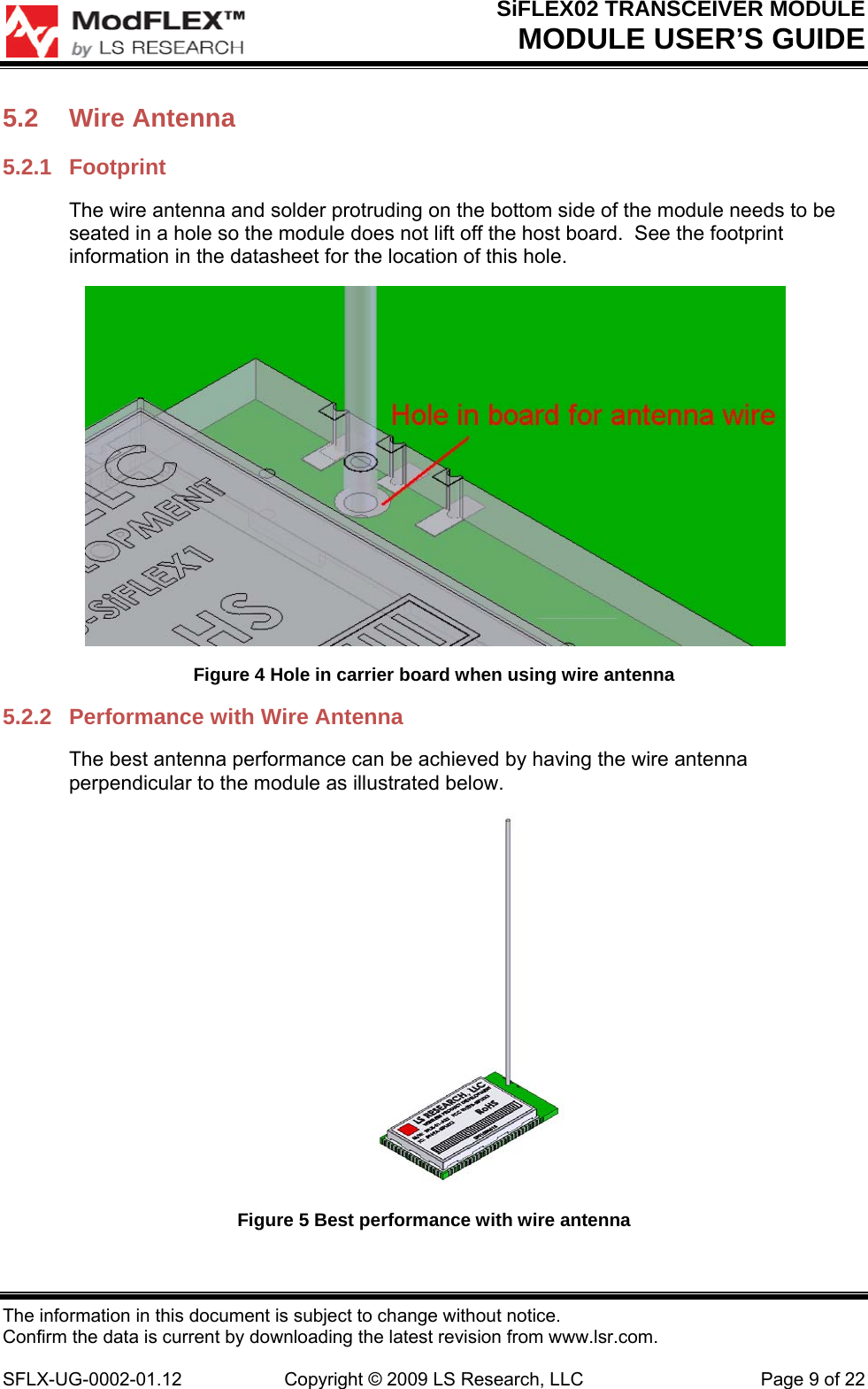
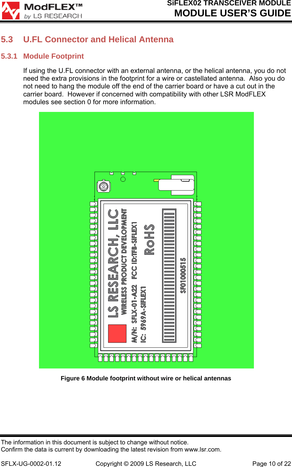
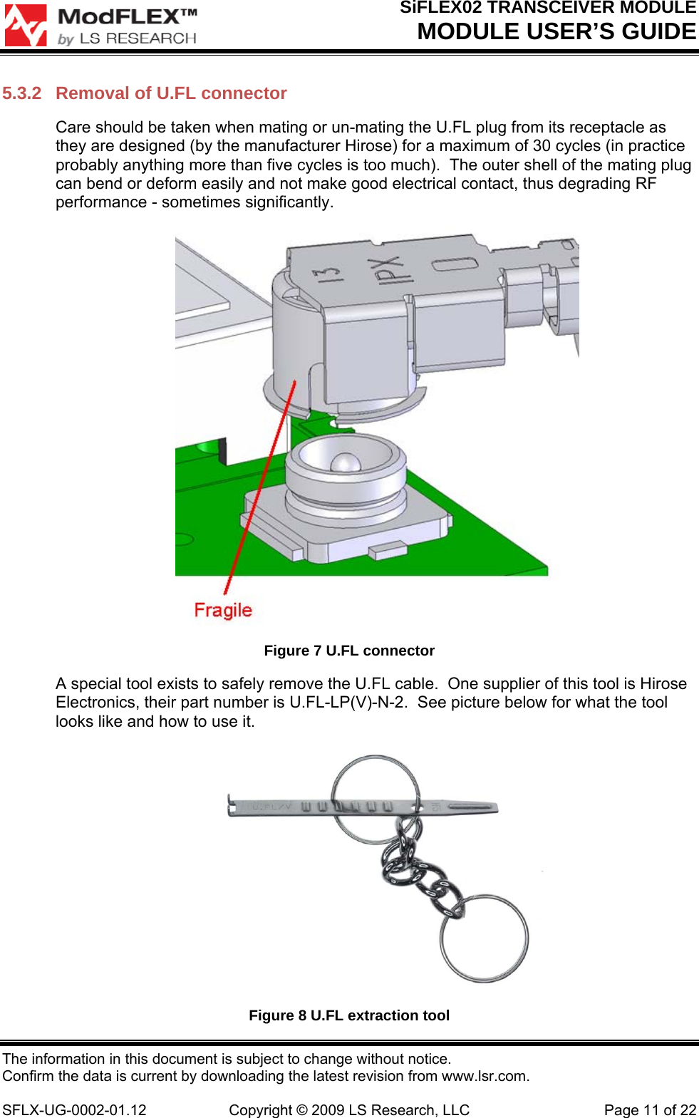
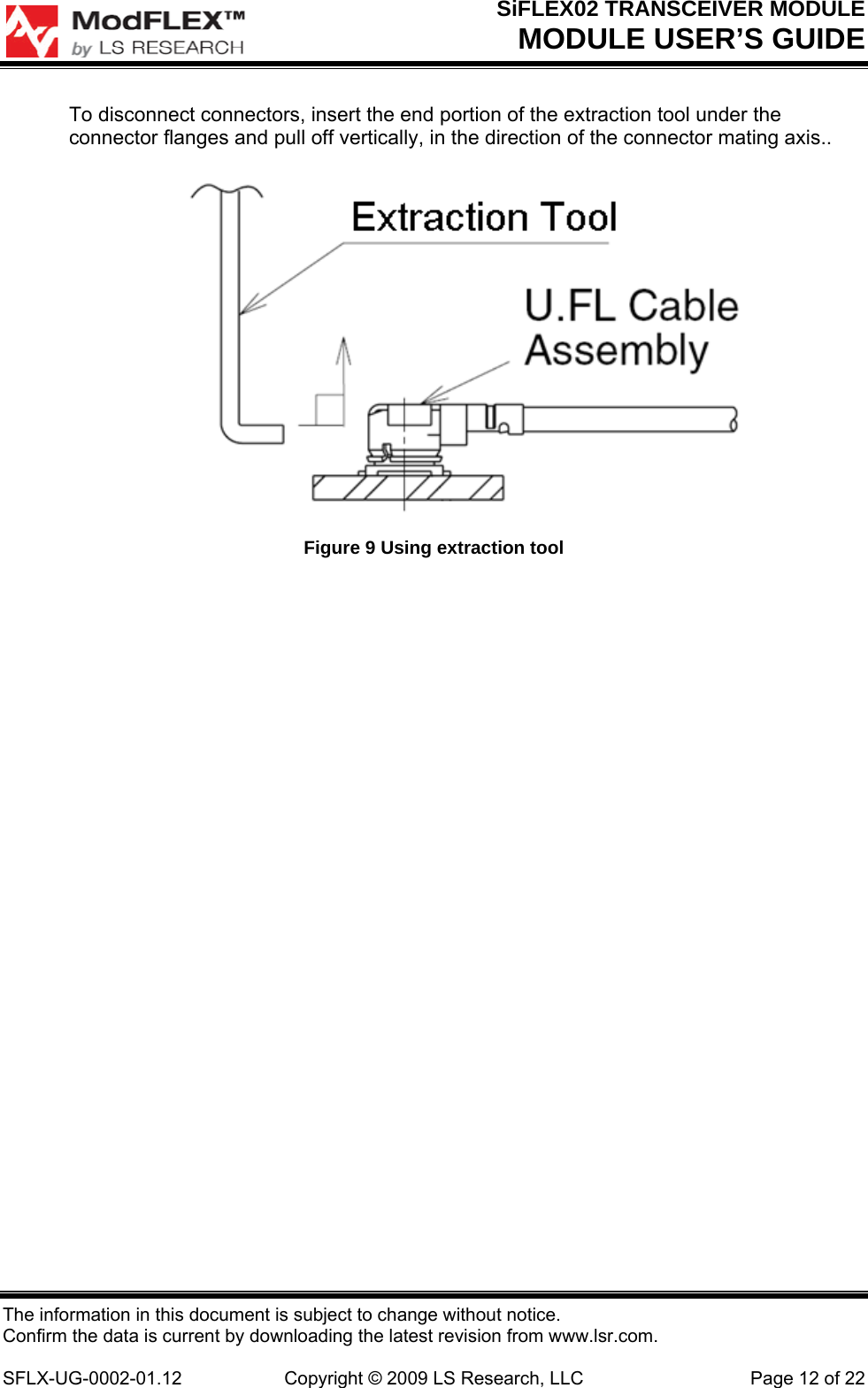
Laird Connectivity SIFLEX2 Modular Transmitter User Manual

LS Research, LLC Modular Transmitter

user manual

 SIFLEX02 TRANSCEIVER MODULE MODULE USER’S GUIDE     Powered By     Last updated Wednesday, November 18, 2009 The information in this document is subject to change without notice. Confirm the data is current by downloading the latest revision from www.lsr.com.  SFLX-UG-0002-01.12  Copyright © 2009 LS Research, LLC  Page 1 of 22
SiFLEX02 TRANSCEIVER MODULE MODULE USER’S GUIDE Table of Contents 1Introduction ..................................................................................................................... 31.1Purpose & Scope ....................................................................................................................... 31.2Audience .................................................................................................................................... 31.3Applicable Documents ...............................................................................................................  31.4Revision History ......................................................................................................................... 32Supporting Ping Pong Range Test on Host Board ...................................................... 43Module Application Circuits ........................................................................................... 53.1CAD Symbols ............................................................................................................................ 53.2Recommended Application Connections - JTAG ...................................................................... 53.3Recommended Application Connections - AVRISP .................................................................. 64Wakeup/Reset Alerts ...................................................................................................... 74.1Wakeup Alert ............................................................................................................................. 74.2Reset Alert ................................................................................................................................. 75Antenna Options and PCB Footprint............................................................................. 85.1Footprint Overview .................................................................................................................... 85.2Wire Antenna ............................................................................................................................. 95.3U.FL Connector and Helical Antenna ......................................................................................  105.4Castellated Antenna ................................................................................................................ 135.5Carrier Board Alignment Holes ................................................................................................ 155.6Compatibility ............................................................................................................................ 186Agency Statements ....................................................................................................... 196.1Federal Communication Commission Interference Statement ................................................ 196.2Industry Canada Statements ................................................................................................... 196.3OEM Responsibilities to comply with FCC and Industry Canada Regulations ....................... 206.4End Product Labeling .............................................................................................................. 207Contacting LS Research ............................................................................................... 22 The information in this document is subject to change without notice. Confirm the data is current by downloading the latest revision from www.lsr.com.  SFLX-UG-0002-01.12  Copyright © 2009 LS Research, LLC  Page 2 of 22
SiFLEX02 TRANSCEIVER MODULE MODULE USER’S GUIDE 1 Introduction 1.1  Purpose & Scope The purpose of this document is to provide details regarding the use of the SiFLEX transceiver module with the host.  This document describes the electrical and wiring considerations when interfacing the SiFLEX module with a host board. 1.2  Audience This document is intended to be read by engineers and technical management.  A general knowledge of common engineering practices is assumed. 1.3  Applicable Documents • SiFLEX Datasheet • SiFLEX Host Protocol User’s Guide 1.4  Revision History Date  Change Description  Revision 8-18-09 Initial release.  1.0 9-21-09  Updated figures 1 and 2.  1.01 11-04-09  Updated section 3 to include information on waking up from sleep.  Added new section on footprint.  1.10 11-16-09  Updated section 6.2 for antenna options.  Updated section 6.4 for FCC/IC numbers  1.11 11-18-09  Added helical antenna option to section 6.2  1.12 Table 1 Revision History The information in this document is subject to change without notice. Confirm the data is current by downloading the latest revision from www.lsr.com.  SFLX-UG-0002-01.12  Copyright © 2009 LS Research, LLC  Page 3 of 22
SiFLEX02 TRANSCEIVER MODULE MODULE USER’S GUIDE 2 Supporting Ping Pong Range Test on Host Board See the Development Kit User’s Guide for detailed information regarding Ping Pong Range Test usage. The Ping Pong Range Test firmware is built into the module firmware.  This allows for the test to be used on the application host board.  The following considerations need to be made in order to utilize the test. 2.1.1  Power A nominal 3.3 VDC power supply should be connected to the VCC - 3V3DC pin (26) on the module.  Also, a ground connection on the GND pin (44) is required.  If batteries are used be sure to install the jumper on J2 between pins 2-3. 2.1.2  LED’s Three LEDs should be connected to module pins 27-29.  The cathode of each LED should be each pin.  The anode of each LED should be connected to the 3.3 V power supply through a nominal resistor value in the range of 180 to 470 ohms.  Module pin 27 should connect to a green LED, pin 28 should connect to a yellow LED, and pin 29 to a red LED. 2.1.3  Switches Module pin 31 should be connected to ground through a normally open tact switch. In addition a 10k ohm pull-up resistor to VCC should be connected to this pin as well.  This switch is referred to as the USER1 button in the subsequent instructions.   Also, the RESET pin should be connected to ground through a momentary contact normally open (NO) push button switch.  This switch is referred to as the RESET button in the subsequent instructions. The information in this document is subject to change without notice. Confirm the data is current by downloading the latest revision from www.lsr.com.  SFLX-UG-0002-01.12  Copyright © 2009 LS Research, LLC  Page 4 of 22
SiFLEX02 TRANSCEIVER MODULE MODULE USER’S GUIDE 3 Module Application Circuits 3.1  CAD Symbols PADS CAD symbols for schematic and PCB can be downloaded from the LSR website www.lsr.com. 3.2  Recommended Application Connections - JTAG Figure 1 shows the minimum circuit connections required for the SiFLEX module, if programming/debugging via AVR JTAGICE mkII.  The LEDs and USER buttons are needed for Ping Pong Range Test, otherwise they are optional.  The LED’s during normal operation flash to indicate module status (UART activity, RF activity, and heartbeat).  Note at the time of this writing the User2 button is not used. The reset (nRESET) pin (14) is active low.  On the SiFLEX module it is pulled high with a 14kΩ resistor.  To reset the module, pull the pin low to ground for at least 100µS.  This is necessary to ensure a proper reset of the module. (Optional LEDs)(Optional buttons)26 VCC UART TX 35UART RX 36PF3 2711 TCK12 TDO PF2 289TMS10 TDI PF1 2913 JTAG/PDI/JRST14 nRESET PE5 3144 GND PF0 30JTAG Header2                        14                        36                        58                        710                      9SiFLEX Module3MN2510-6002-UBTXRXModule ResetVCCGNDUSER1Host470 Ω10 kΩ47 nF470 Ω470 ΩUSER247 nF10 kΩGreenRedYellowRESET1 kΩ(Optional button)1 kΩ Figure 1 Sample Application Circuit with JTAG   The information in this document is subject to change without notice. Confirm the data is current by downloading the latest revision from www.lsr.com.  SFLX-UG-0002-01.12  Copyright © 2009 LS Research, LLC  Page 5 of 22
SiFLEX02 TRANSCEIVER MODULE MODULE USER’S GUIDE 3.3  Recommended Application Connections - AVRISP Figure 2 shows the minimum circuit connections required for the SiFLEX module, if programming with the AVRISP mkII.  The AVRISP mkII can only be used for programming; in-circuit debugging must be done via JTAG.  This circuit is identical to the one in Figure 1, with the exception of the connection for the AVRISP mkII. (Optional LEDs)(Optional buttons)26 VCC UART TX 35UART RX 36PF3 2713 JTAG/PDI/JRSTPF2 2814 nRESETPF1 29PE5 3144 GND PF0 30ISP HeaderSiFLEX ModuleTXRXModule ResetVCCGNDUSER1Host470 Ω10 kΩ47 nF470 Ω470 ΩUSER247 nF10 kΩGreenRedYellow214365RESET1 kΩ(Optional button)1 kΩ Figure 2 Sample Application Circuit with AVRISP The information in this document is subject to change without notice. Confirm the data is current by downloading the latest revision from www.lsr.com.  SFLX-UG-0002-01.12  Copyright © 2009 LS Research, LLC  Page 6 of 22
SiFLEX02 TRANSCEIVER MODULE MODULE USER’S GUIDE 4 Wakeup/Reset Alerts See host message types 0x1C (Set Wakeup/Reset Settings) and 0x9E (Wakeup/Reset Alert Status) in the SiFLEX Host Protocol User’s Guide to use the features described below. 4.1  Wakeup Alert The Wakeup Alert Status message can be used to alert the host microcontroller when it wakes up from sleep.  This useful for two main reasons: •  The host microcontroller knows that the SiFLEX module is ready to operate and can then accept commands over the host interface. •  The host microcontroller knows the SiFLEX module has woken up from sleep due to an errant condition.  For example if noise appeared on the SiFLEX wakeup input pin and the host microcontroller did not know it was out of sleep and drawing current, the power budget could be exceeded. To wake the SiFLEX module out of sleep simply send a dummy byte to the module.  The SiFLEX module will wake up from sleep in under 1mS, at which point the Wakeup Alert Status message will be sent to the host, if enabled. 4.2  Reset Alert The Reset Alert Status message can also be used to alert the host microcontroller when the module has been reset.  This useful so the host microcontroller knows that the SiFLEX module is ready to operate and can then accept commands over the host interface. The information in this document is subject to change without notice. Confirm the data is current by downloading the latest revision from www.lsr.com.  SFLX-UG-0002-01.12  Copyright © 2009 LS Research, LLC  Page 7 of 22
SiFLEX02 TRANSCEIVER MODULE MODULE USER’S GUIDE 5 Antenna Options and PCB Footprint 5.1  Footprint Overview The footprint design on the carrier board will depend on the carrier board requirements, desire for compatibility with other ModFLEX series modules, and the desired antenna.  Figure 3 Footprint Overview   The information in this document is subject to change without notice. Confirm the data is current by downloading the latest revision from www.lsr.com.  SFLX-UG-0002-01.12  Copyright © 2009 LS Research, LLC  Page 8 of 22
SiFLEX02 TRANSCEIVER MODULE MODULE USER’S GUIDE 5.2  Wire Antenna 5.2.1  Footprint The wire antenna and solder protruding on the bottom side of the module needs to be seated in a hole so the module does not lift off the host board.  See the footprint information in the datasheet for the location of this hole.  Figure 4 Hole in carrier board when using wire antenna 5.2.2  Performance with Wire Antenna The best antenna performance can be achieved by having the wire antenna perpendicular to the module as illustrated below.  Figure 5 Best performance with wire antenna The information in this document is subject to change without notice. Confirm the data is current by downloading the latest revision from www.lsr.com.  SFLX-UG-0002-01.12  Copyright © 2009 LS Research, LLC  Page 9 of 22
SiFLEX02 TRANSCEIVER MODULE MODULE USER’S GUIDE 5.3  U.FL Connector and Helical Antenna 5.3.1  Module Footprint If using the U.FL connector with an external antenna, or the helical antenna, you do not need the extra provisions in the footprint for a wire or castellated antenna.  Also you do not need to hang the module off the end of the carrier board or have a cut out in the carrier board.  However if concerned with compatibility with other LSR ModFLEX modules see section 0 for more information.  Figure 6 Module footprint without wire or helical antennas   The information in this document is subject to change without notice. Confirm the data is current by downloading the latest revision from www.lsr.com.  SFLX-UG-0002-01.12  Copyright © 2009 LS Research, LLC  Page 10 of 22
SiFLEX02 TRANSCEIVER MODULE MODULE USER’S GUIDE 5.3.2  Removal of U.FL connector Care should be taken when mating or un-mating the U.FL plug from its receptacle as they are designed (by the manufacturer Hirose) for a maximum of 30 cycles (in practice probably anything more than five cycles is too much).  The outer shell of the mating plug can bend or deform easily and not make good electrical contact, thus degrading RF performance - sometimes significantly.  Figure 7 U.FL connector A special tool exists to safely remove the U.FL cable.  One supplier of this tool is Hirose Electronics, their part number is U.FL-LP(V)-N-2.  See picture below for what the tool looks like and how to use it.  Figure 8 U.FL extraction tool The information in this document is subject to change without notice. Confirm the data is current by downloading the latest revision from www.lsr.com.  SFLX-UG-0002-01.12  Copyright © 2009 LS Research, LLC  Page 11 of 22
SiFLEX02 TRANSCEIVER MODULE MODULE USER’S GUIDE To disconnect connectors, insert the end portion of the extraction tool under the connector flanges and pull off vertically, in the direction of the connector mating axis..  Figure 9 Using extraction tool   The information in this document is subject to change without notice. Confirm the data is current by downloading the latest revision from www.lsr.com.  SFLX-UG-0002-01.12  Copyright © 2009 LS Research, LLC  Page 12 of 22
SiFLEX02 TRANSCEIVER MODULE MODULE USER’S GUIDE 5.4  Castellated Antenna The castellated antenna option allows the use of a RF connector or PCB trace antenna on the modules carrier board.  This option is NOT included with the Module’s FCC/IC Certification.  It will require an additional certification.  LS Research is equipped with a certification lab and can assist in getting this done at a reasonable cost in a short period of time. The castellated antenna option is NOT available on all ModFLEX modules from LS Research.   See section 5.6 for more information. Use of the castellated antenna will require the three pads shown in the figure below.  If the castellated antenna option is not needed the pads may be eliminated from the footprint.  Figure 10 Pads intended for castellated antenna option The information in this document is subject to change without notice. Confirm the data is current by downloading the latest revision from www.lsr.com.  SFLX-UG-0002-01.12  Copyright © 2009 LS Research, LLC  Page 13 of 22
SiFLEX02 TRANSCEIVER MODULE MODULE USER’S GUIDE Special care in routing the RF signal on the carrier board is needed.  LS Research has a full palette of design services, including RF board layout, and would be happy to assist.  Other guidelines are listed below: •  Keep the RF trace as short as possible. •  Ensure the impedance of the RF trace is kept at 50 ohms.  Figure 11 Using the castellated antenna   The information in this document is subject to change without notice. Confirm the data is current by downloading the latest revision from www.lsr.com.  SFLX-UG-0002-01.12  Copyright © 2009 LS Research, LLC  Page 14 of 22
SiFLEX02 TRANSCEIVER MODULE MODULE USER’S GUIDE 5.5  Carrier Board Alignment Holes The ModFLEX modules have two 0.032” diameter non-plated holes in the PCB that can be used to align the module to the carrier board.  When designing the carrier board it is recommended to include two matching alignment holes with copper pads surrounding the holes on the bottom side of the board.  The purpose of the copper pads allows for soldering alignment pins when the carrier board is used as an alignment fixture, which is described in the following sections.  Figure 12 Alignment holes on module and carrier board    The information in this document is subject to change without notice. Confirm the data is current by downloading the latest revision from www.lsr.com.  SFLX-UG-0002-01.12  Copyright © 2009 LS Research, LLC  Page 15 of 22
SiFLEX02 TRANSCEIVER MODULE MODULE USER’S GUIDE 5.5.1  Constructing an alignment fixture Any carrier board can be made into an alignment fixture.  When using the carrier board as an alignment fixture the alignment pins can be soldered to the bare carrier board to prevent them from falling out.  Then by adding standoffs to the bare carrier board you have created an alignment fixture.  Figure 13 Alignment fixture overview Step 1:  Make an alignment fixture by soldering two Mill-Max 3120-2 series pins or equivalent into the PCB being used for the alignment fixture.  For spacing, use 1/8” standoffs between this board and the target carrier board.  Figure 14 Constructing an alignment fixture Step 2:  Carefully place the target carrier board through the pins on the alignment fixture. The information in this document is subject to change without notice. Confirm the data is current by downloading the latest revision from www.lsr.com.  SFLX-UG-0002-01.12  Copyright © 2009 LS Research, LLC  Page 16 of 22
SiFLEX02 TRANSCEIVER MODULE MODULE USER’S GUIDE  Figure 15 Placing target carrier board Step 3:  Drop the ModFLEX module onto the carrier board through the alignment pins and solder the module to the carrier board.  Figure 16 Placing target module   The information in this document is subject to change without notice. Confirm the data is current by downloading the latest revision from www.lsr.com.  SFLX-UG-0002-01.12  Copyright © 2009 LS Research, LLC  Page 17 of 22
SiFLEX02 TRANSCEIVER MODULE MODULE USER’S GUIDE 5.6  Compatibility Not all ModFLEX modules have the same antenna options.  To use the modules interchangeably on a carrier board, the designs outlined below must be employed.  Option 1:  The carrier board should be designed so the module overhangs the edge of the board 0.23” as pictured below. Figure 17 Overhang the Module (dimensions in inches) Option 2:  Design an opening in the carrier board.  A minimum opening is shown below.  Figure 18 Opening in the carrier board. The information in this document is subject to change without notice. Confirm the data is current by downloading the latest revision from www.lsr.com.  SFLX-UG-0002-01.12  Copyright © 2009 LS Research, LLC  Page 18 of 22
SiFLEX02 TRANSCEIVER MODULE MODULE USER’S GUIDE 6 Agency Statements 6.1  Federal Communication Commission Interference Statement This equipment has been tested and found to comply with the limits for a Class B digital device, pursuant to Part 15 of the FCC Rules. These limits are designed to provide reasonable protection against harmful interference in a residential installation. This equipment generates uses and can radiate radio frequency energy and, if not installed and used in accordance with the instructions, may cause harmful interference to radio communications. However, there is no guarantee that interference will not occur in a particular installation. If this equipment does cause harmful interference to radio or television reception, which can be determined by turning the equipment off and on, the user is encouraged to try to correct the interference by one of the following measures: •  Reorient or relocate the receiving antenna. •  Increase the separation between the equipment and receiver. •  Connect the equipment into an outlet on a circuit different from that to which the receiver is connected. •  Consult the dealer or an experienced radio/TV technician for help. This device complies with Part 15 of the FCC Rules. Operation is subject to the following two conditions: (1) This device may not cause harmful interference, and (2) this device must accept any interference received, including interference that may cause undesired operation. FCC CAUTION: Any changes or modifications not expressly approved by the party responsible for compliance could void the user's authority to operate this equipment. 6.2  Industry Canada Statements Operation is subject to the following two conditions: (1) this device may not cause interference, and (2) this device must accept any interference, including interference that may cause undesired operation of the device. To reduce potential radio interference to other users, the antenna type and its gain should be so chosen that the equivalent isotropically radiated power (e.i.r.p.) is not more than that permitted for successful communication. This device has been designed to operate with the antennas listed below, and having a maximum gain of 2 dB. Antennas not included in this list or having a gain greater than 2 dB are strictly prohibited for use with this device. The required antenna impedance is 50 ohms. •  Wire monopole – 3.2 inch, 22 AWG solid copper wire, pvc insulated. •  External dipole – Nearson S467AH-915, RP-SMA on 6” cable. The information in this document is subject to change without notice. Confirm the data is current by downloading the latest revision from www.lsr.com.  SFLX-UG-0002-01.12  Copyright © 2009 LS Research, LLC  Page 19 of 22
SiFLEX02 TRANSCEIVER MODULE MODULE USER’S GUIDE •  On board chip helical – Pulse Engineering W3112A 6.3  OEM Responsibilities to comply with FCC and Industry Canada Regulations The SiFLEX Module has been certified for integration into products only by OEM integrators under the following conditions:  1.  The antenna(s) must be installed such that a minimum separation distance of 20cm is maintained between the radiator (antenna) and all persons at all times. 2.  The transmitter module must not be co-located or operating in conjunction with any other antenna or transmitter.  As long as the two conditions above are met, further transmitter testing will not be required. However, the OEM integrator is still responsible for testing their end-product for any additional compliance requirements required with this module installed (for example, digital device emissions, PC peripheral requirements, etc.). IMPORTANT NOTE: In the event that these conditions cannot be met (for certain configurations or co-location with another transmitter), then the FCC and Industry Canada authorizations are no longer considered valid and the FCC ID and IC Certification Number cannot be used on the final product. In these circumstances, the OEM integrator will be responsible for re-evaluating the end product (including the transmitter) and obtaining a separate FCC and Industry Canada authorization. 6.4  End Product Labeling The SiFLEX Module is labeled with its own FCC ID and IC Certification Number. If the FCC ID and IC Certification Number are not visible when the module is installed inside another device, then the outside of the device into which the module is installed must also display a label referring to the enclosed module.  In that case, the final end product must be labeled in a visible area with the following:  “Contains Transmitter Module FCC ID: TFB-SiFLEX2” “Contains Transmitter Module IC: 5969A-SiFLEX2” or  “Contains FCC ID: TFB-SiFLEX2” “Contains IC: 5969A-SiFLEX2” The OEM of the SiFLEX Module must only use the approved antenna(s) listed above, which have been certified with this module. The information in this document is subject to change without notice. Confirm the data is current by downloading the latest revision from www.lsr.com.  SFLX-UG-0002-01.12  Copyright © 2009 LS Research, LLC  Page 20 of 22
SiFLEX02 TRANSCEIVER MODULE MODULE USER’S GUIDE The OEM integrator has to be aware not to provide information to the end user regarding how to install or remove this RF module or change RF related parameters in the user manual of the end product. The user manual for the end product must include the following information in a prominent location: To comply with FCC and Industry Canada RF radiation exposure limits for general population, the antenna(s) used for this transmitter must be installed such that a minimum separation distance of 20cm is maintained between the radiator (antenna) and all persons at all times and must not be co-located or operating in conjunction with any other antenna or transmitter. The information in this document is subject to change without notice. Confirm the data is current by downloading the latest revision from www.lsr.com.  SFLX-UG-0002-01.12  Copyright © 2009 LS Research, LLC  Page 21 of 22
SiFLEX02 TRANSCEIVER MODULE MODULE USER’S GUIDE The information in this document is subject to change without notice. Confirm the data is current by downloading the latest revision from www.lsr.com.  SFLX-UG-0002-01.12  Copyright © 2009 LS Research, LLC  Page 22 of 22 7 Contacting LS Research Headquarters  LS Research, LLC   W66 N220 Commerce Court   Cedarburg, WI 53012-2636  USA  Tel: 1(262) 375-4400   Fax: 1(262) 375-4248 Website www.lsr.com Technical Support support@lsr.com Sales Contact sales@lsr.com                    The information in this document is provided in connection with LS Research (hereafter referred to as “LSR”) products. No license, express or implied, by estoppel or otherwise, to any intellectual property right is granted by this document or in connection with the sale of LSR products. EXCEPT AS SET FORTH IN LSR’S TERMS AND CONDITIONS OF SALE LOCATED ON LSR’S WEB SITE, LSR ASSUMES NO LIABILITY WHATSOEVER AND DISCLAIMS ANY EXPRESS, IMPLIED OR STATUTORY WARRANTY RELATING TO ITS PRODUCTS INCLUDING, BUT NOT LIMITED TO, THE IMPLIED WARRANTY OF MERCHANTABILITY, FITNESS FOR A PARTICULAR PURPOSE, OR NON-INFRINGEMENT. IN NO EVENT SHALL LSR BE LIABLE FOR ANY DIRECT, INDIRECT, CONSEQUENTIAL, PUNITIVE, SPECIAL OR INCIDENTAL DAMAGES (INCLUDING, WITHOUT LIMITATION, DAMAGES FOR LOSS OF PROFITS, BUSINESS INTERRUPTION, OR LOSS OF INFORMATION) ARISING OUT OF THE USE OR INABILITY TO USE THIS DOCUMENT, EVEN IF LSR HAS BEEN ADVISED OF THE POSSIBILITY OF SUCH DAMAGES. LSR makes no representations or warranties with respect to the accuracy or completeness of the contents of this document and reserves the right to make changes to specifications and product descriptions at any time without notice. LSR does not make any commitment to update the information contained herein. Unless specifically provided otherwise, LSR products are not suitable for, and shall not be used in, automotive applications. LSR’s products are not intended, authorized, or warranted for use as components in applications intended to support or sustain life.

Navigation menu