Laird Connectivity TIWI501 TiWi5 Transceiver Module User Manual
LS Research, LLC TiWi5 Transceiver Module
UserManual.wiki
>
Laird Connectivity
>
TIWI501 User Manual
>
User Manual
Contents
1.
User Manual
2.
User Manual R2
3.
Users Manual
User Manual
Navigation menu
Upload a User Manual
Namespaces
Wiki Guide
HTML
PDF
Info
Views
User Manual
Discussion / Help
Navigation
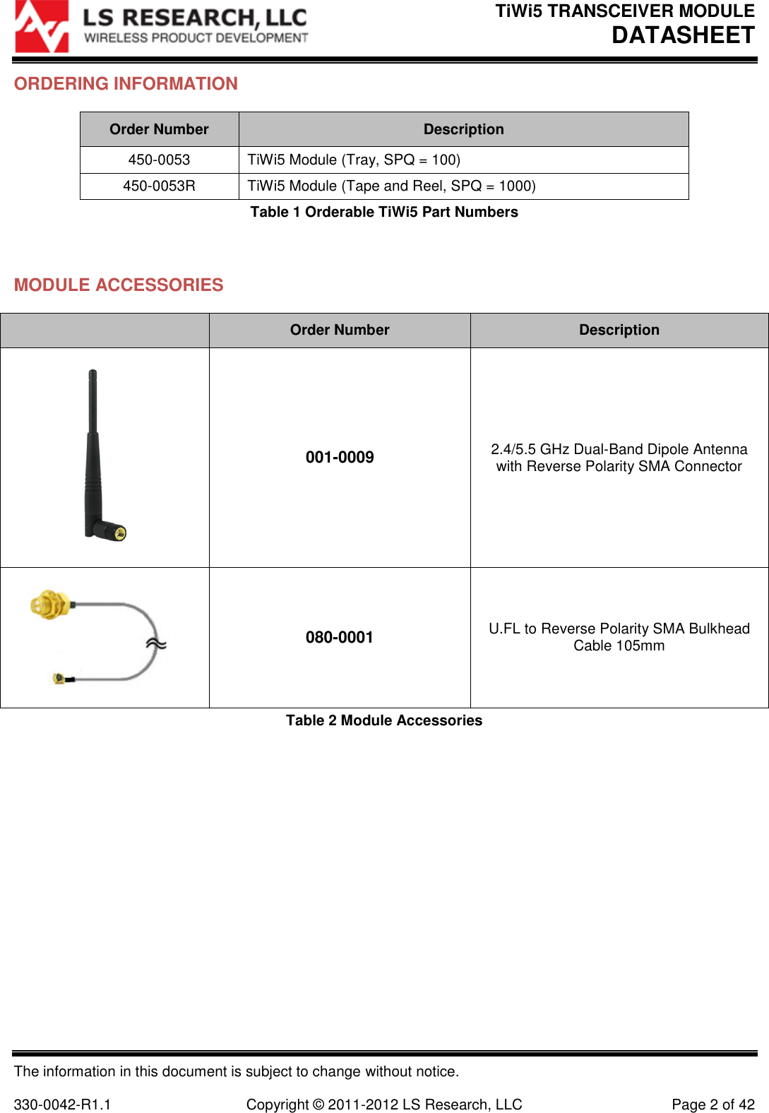
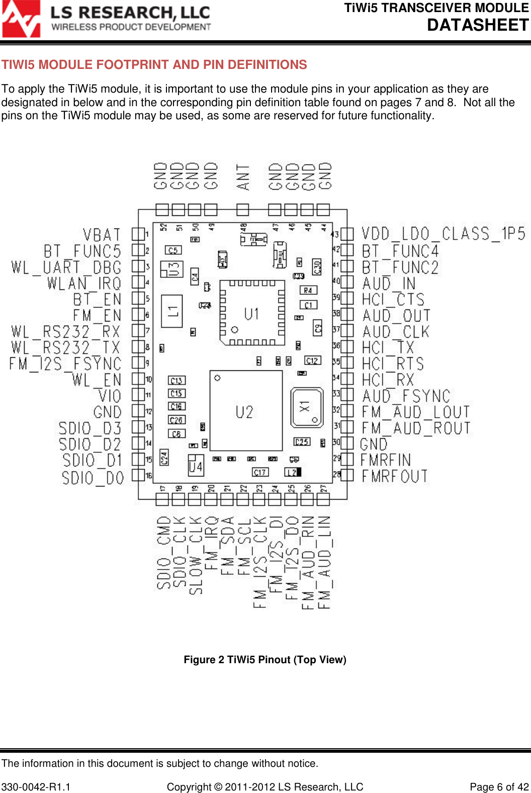
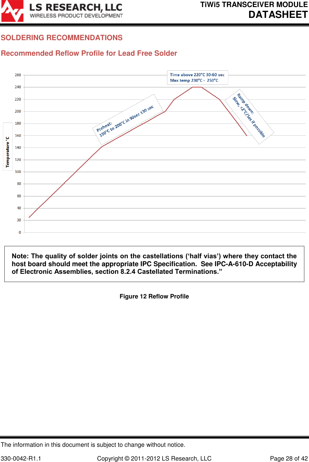
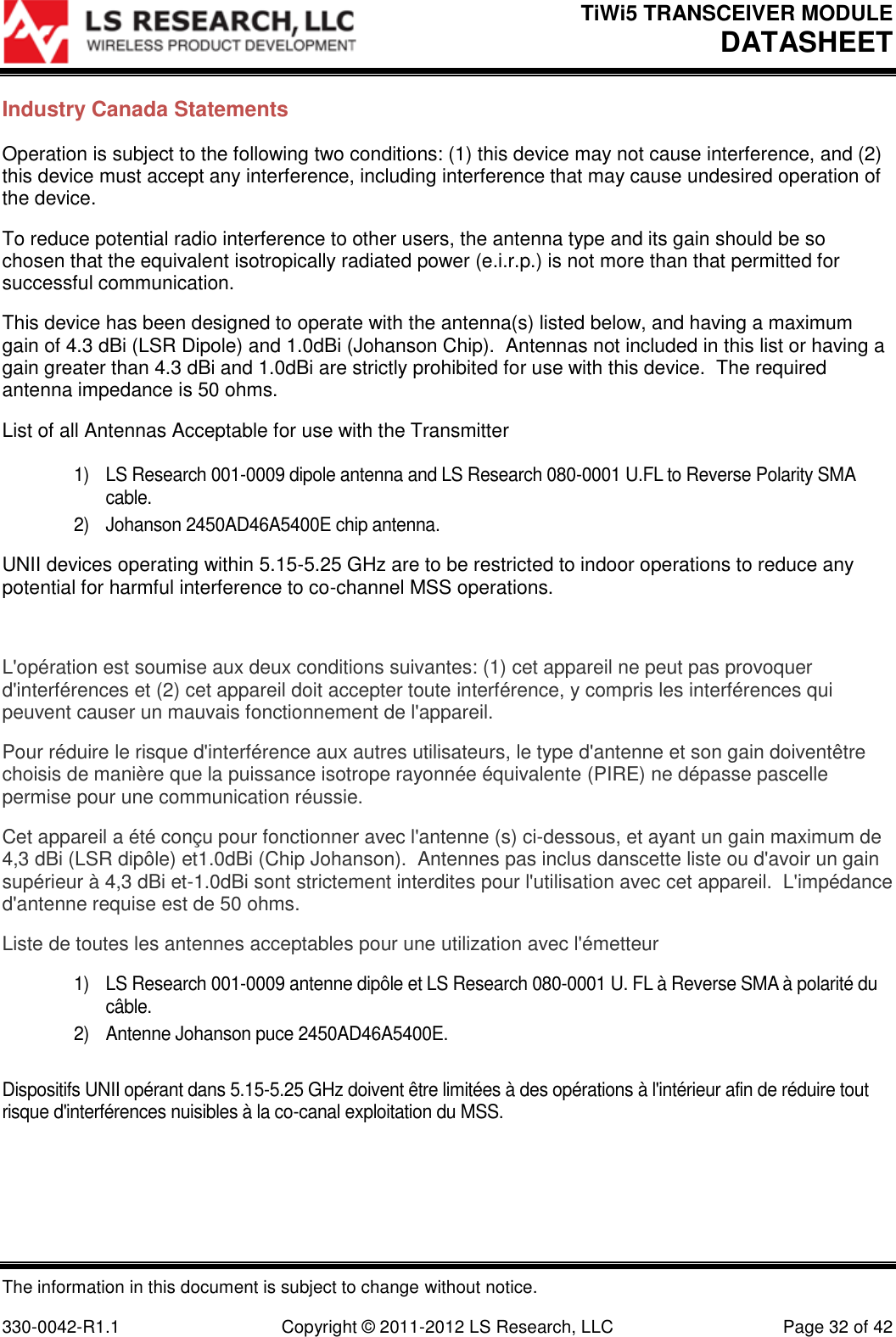
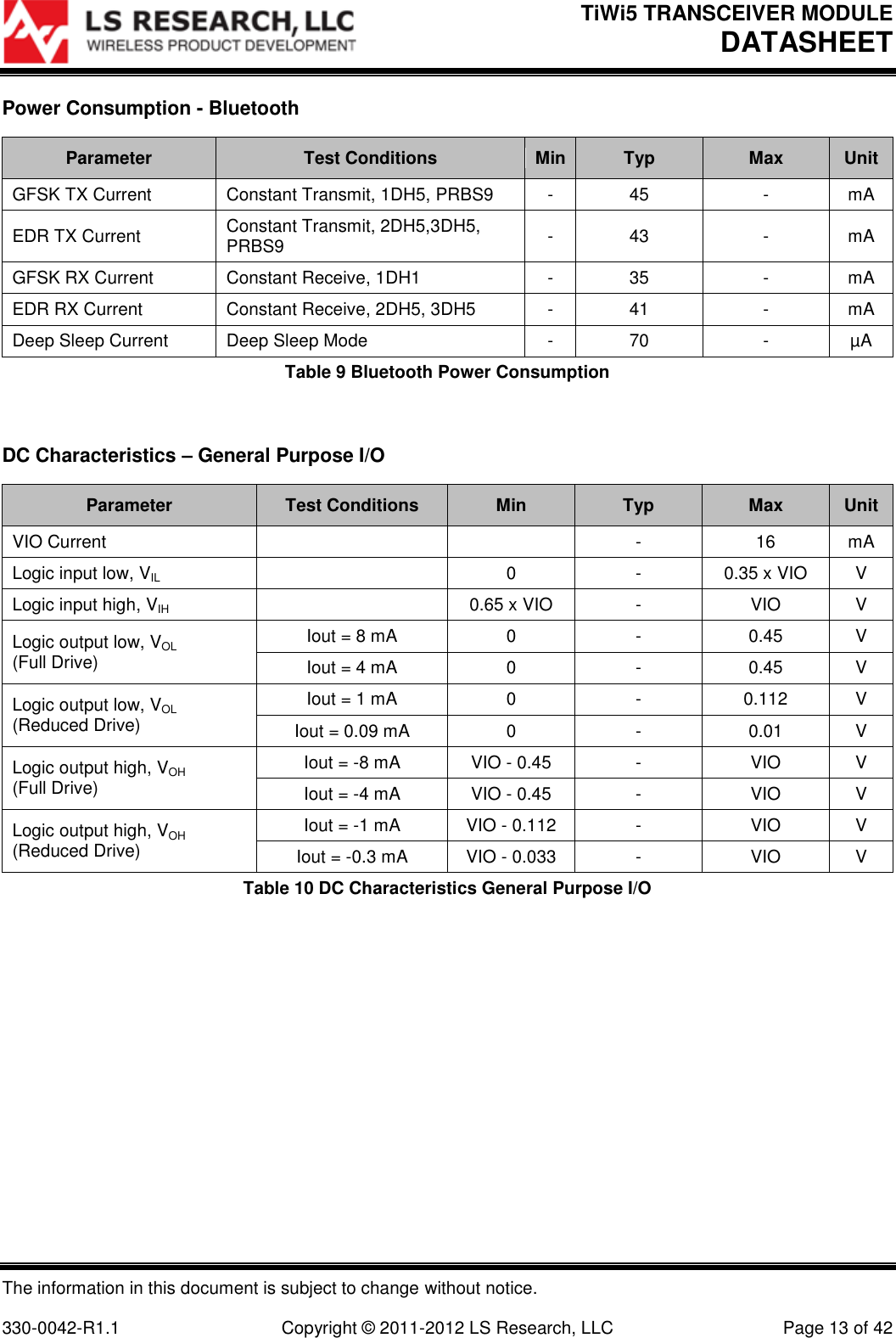
![TiWi5 TRANSCEIVER MODULE DATASHEET The information in this document is subject to change without notice. 330-0042-R1.1 Copyright © 2011-2012 LS Research, LLC Page 8 of 42 Module Pin Name I/O Type Buffer Type Logic Level Description 32 FM_AUD_LOUT AO - - NOT SUPPORTED, NO CONNECT 33 AUD_FSYNC DIO 4 mA 1.8 VDC PCM I/F 34 HCI_RX DI 8 mA 1.8 VDC Bluetooth HCI UART RX (*) 35 HCI_RTS DO 4 mA 1.8 VDC Bluetooth HCI UART RTS (*) 36 HCI_TX DIO 8 mA 1.8 VDC Bluetooth HCI UART TX 37 AUD_CLK DO 4 mA 1.8 VDC PCM I/F (*) 38 AUD_OUT DO 4 mA 1.8 VDC PCM I/F (*) 39 HCI_CTS DI 4 mA 1.8 VDC Bluetooth HCI UART CTS (*) 40 AUD_IN DI 4 mA 1.8 VDC PCM I/F (*) 41 BT_FUNC2 DI 4 mA 1.8 VDC Bluetooth Wakeup / DC2DC mode (*) 42 BT_FUNC4 DO 4 mA 1.8 VDC BT_UARTD (DEBUG) (*) 43 VDD_LDO_CLASS_1P5 NC - - VBAT VOLTAGE PRESENT, NO CONNECT 44 GND GND - - Ground 45 GND GND - - Ground 46 GND GND - - Ground 47 GND GND - - Ground 48 ANT RF - Antenna terminal for WLAN and Bluetooth (note [1]) 49 GND GND - - Ground 50 GND GND - - Ground 51 GND GND - - Ground 52 GND GND - - Ground PI = Power Input PO = Power Output DI = Digital Input (1.8 VDC Logic Level) DO = Digital Output (1.8 VDC Logic Level) AI = Analog Input AO = Analog Output AIO = Analog Input/Output RF = RF Port GND = Ground Note[1]: Antenna terminal presents DC short circuit to ground. (*) indicates that pin is capable of bidirectional operation, but is used as the type shown. Table 3 TiWi5 Module Pin Descriptions All digital I/O signals use 1.8V logic. If the host microcontroller does not support 1.8V logic, then level shifters MUST be used.](https://usermanual.wiki/Laird-Connectivity/TIWI501.User-Manual/User-Guide-1763941-Page-8.png)
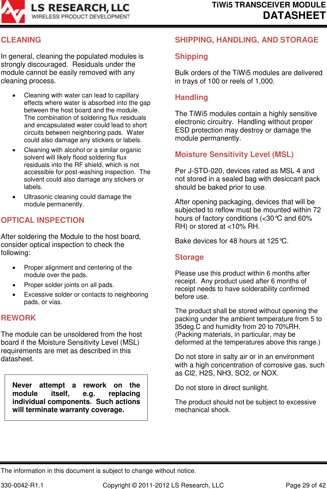
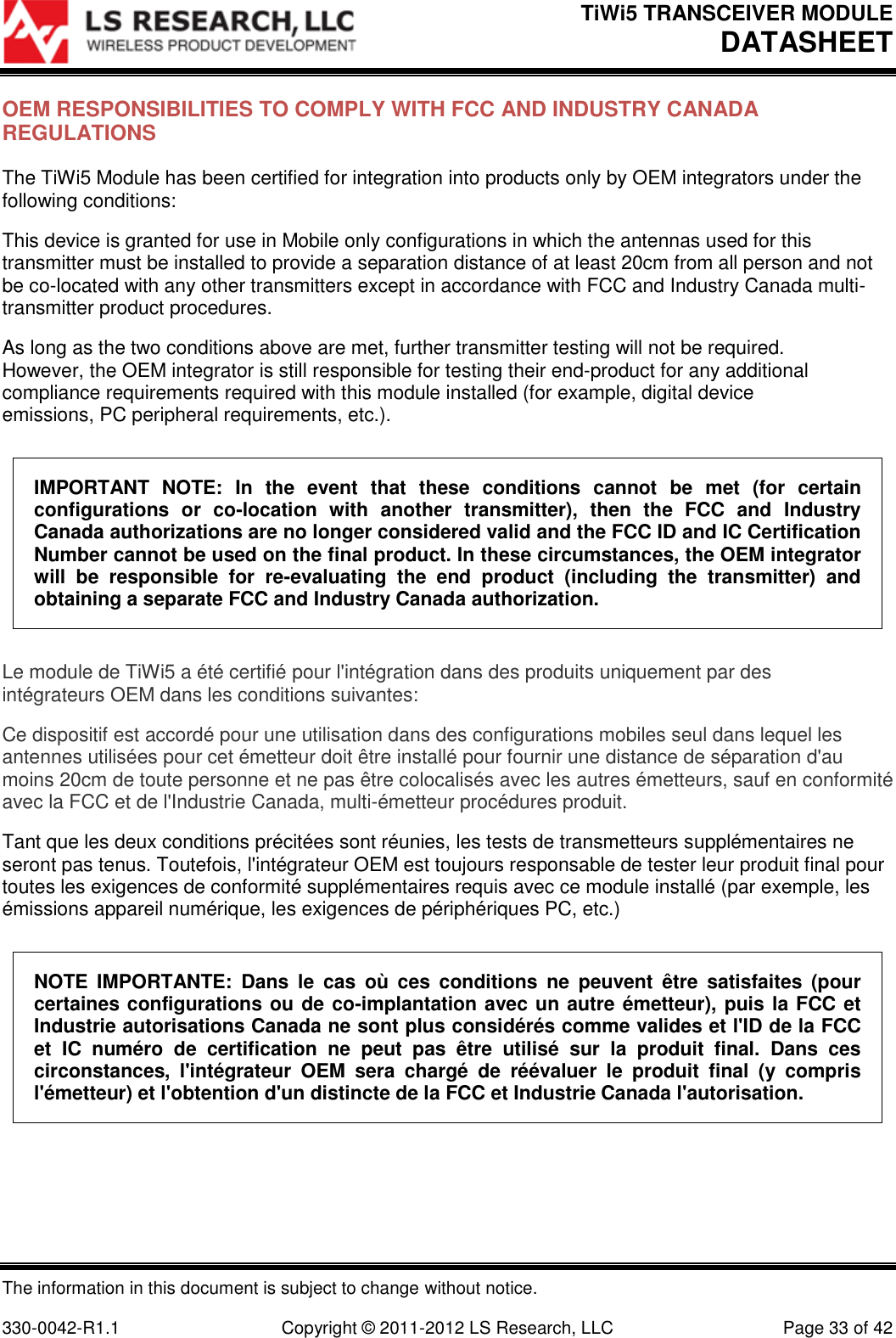
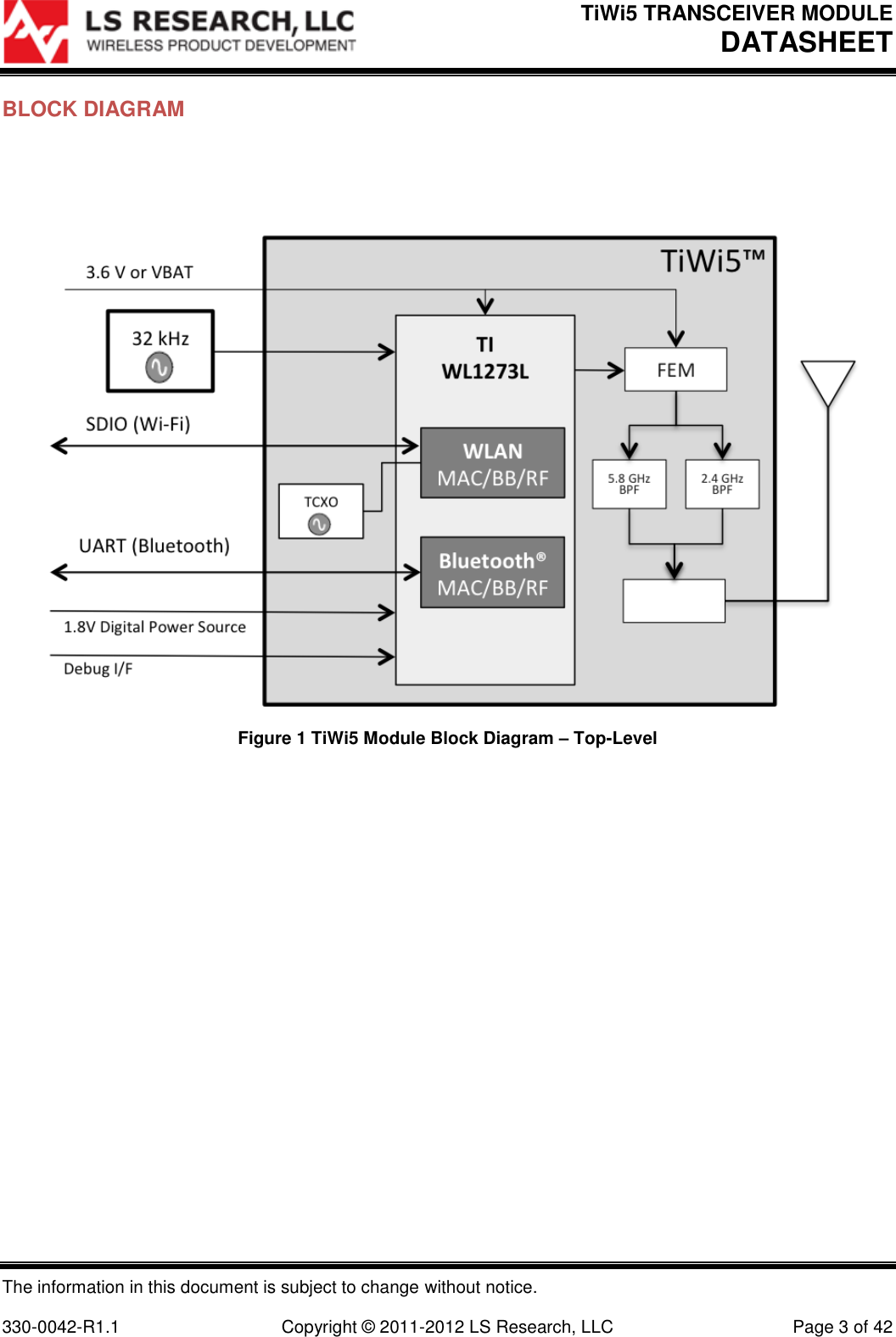
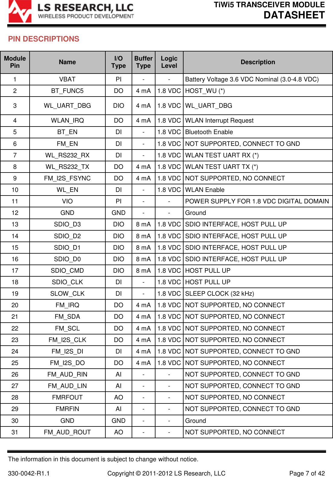
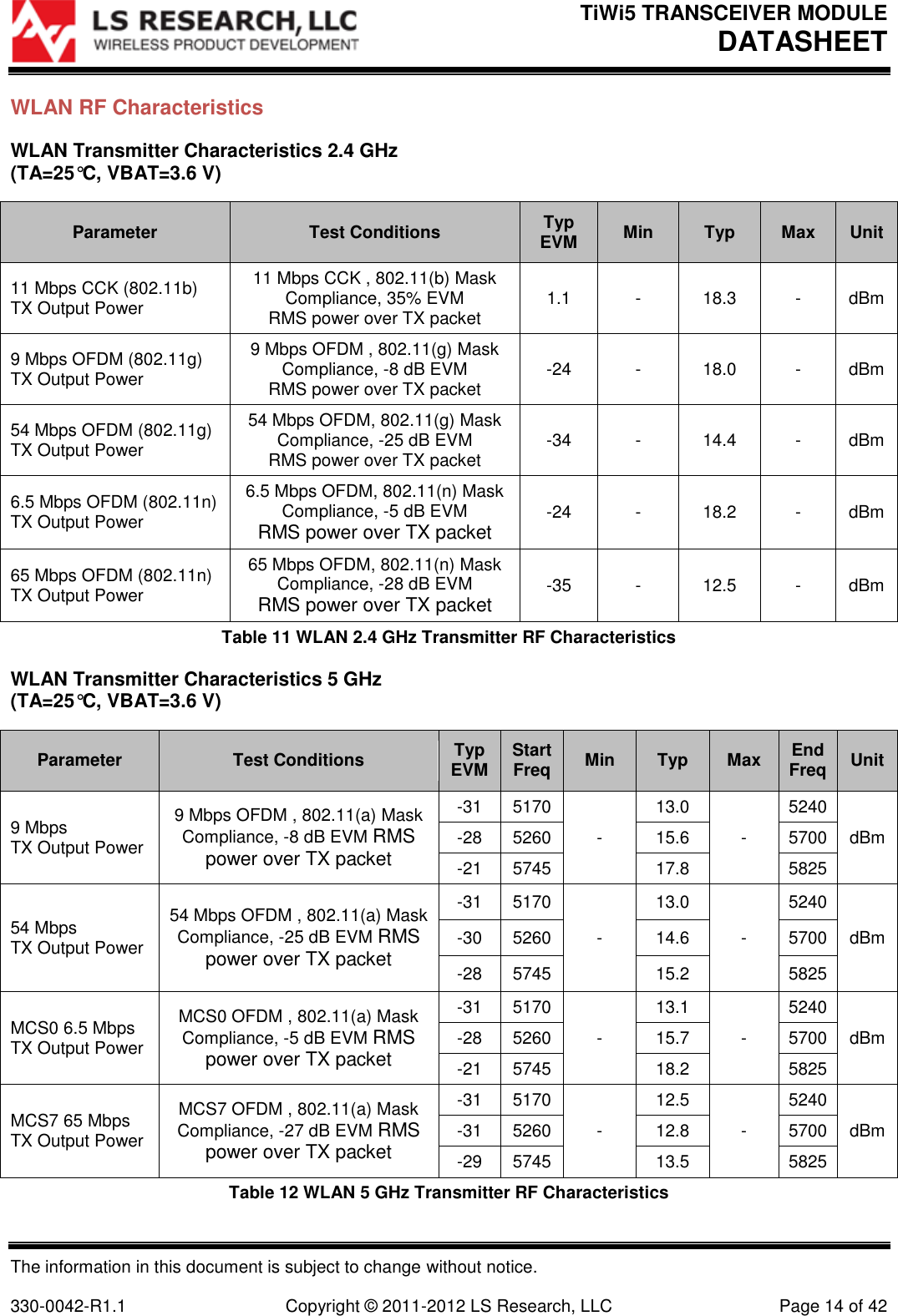
![TiWi5 TRANSCEIVER MODULE DATASHEET The information in this document is subject to change without notice. 330-0042-R1.1 Copyright © 2011-2012 LS Research, LLC Page 11 of 42 General Characteristics Parameter Min Typ Max Unit WLAN RF frequency range 1 2412 2472 MHz WLAN RF frequency range 2 4910 5835 MHz WLAN RF data rate 1 802.11 a/b/g/n rates supported 65 Mbps BT RF frequency Range 2402 2480 MHz Table 6 General Characteristics Power Consumption – WLAN 2.4 GHz Parameter Test Conditions Min Typ Max Unit CCK (802.11b) TX Current 2437 MHz, VBAT =3.6V, Tamb=+25°C Po=18.3 dBm, 11 Mbps CCK L=1200 bytes, tdelay (idle)=4 S - 247 - mA OFDM (802.11g) TX Current 2437 MHz, VBAT =3.6V, Tamb=+25°C Po=14.4 dBm, 54 Mbps OFDM L=1200 bytes, tdelay (idle)=4 S - 180 - mA OFDM (802.11n) TX Current 2437 MHz, VBAT =3.6V, Tamb=+25°C Po=12.5 dBm, 65 Mbps OFDM L=1200 bytes, tdelay (idle)=4 S - 166 - mA CCK (802.11b) RX Current - 93 - mA OFDM (802.11g) RX Current - 93 - mA OFDM (802.11n) RX Current - 93 - mA Dynamic Mode [1] - <1.2 - mA [1] Total Current from VBAT for reception of Beacons with DTIM=1 TBTT=100 mS, Beacon duration 1.6ms, 1 Mbps beacon reception in Listen Mode. Table 7 2.4 GHz WLAN Power Consumption](https://usermanual.wiki/Laird-Connectivity/TIWI501.User-Manual/User-Guide-1763941-Page-11.png)
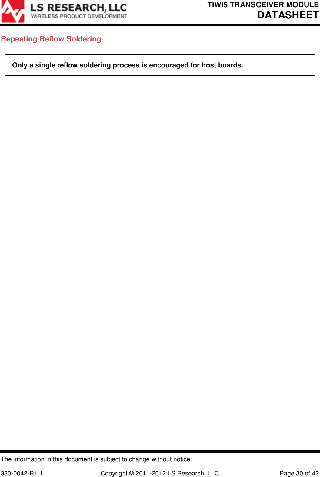
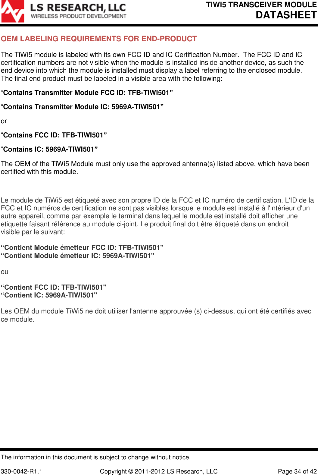
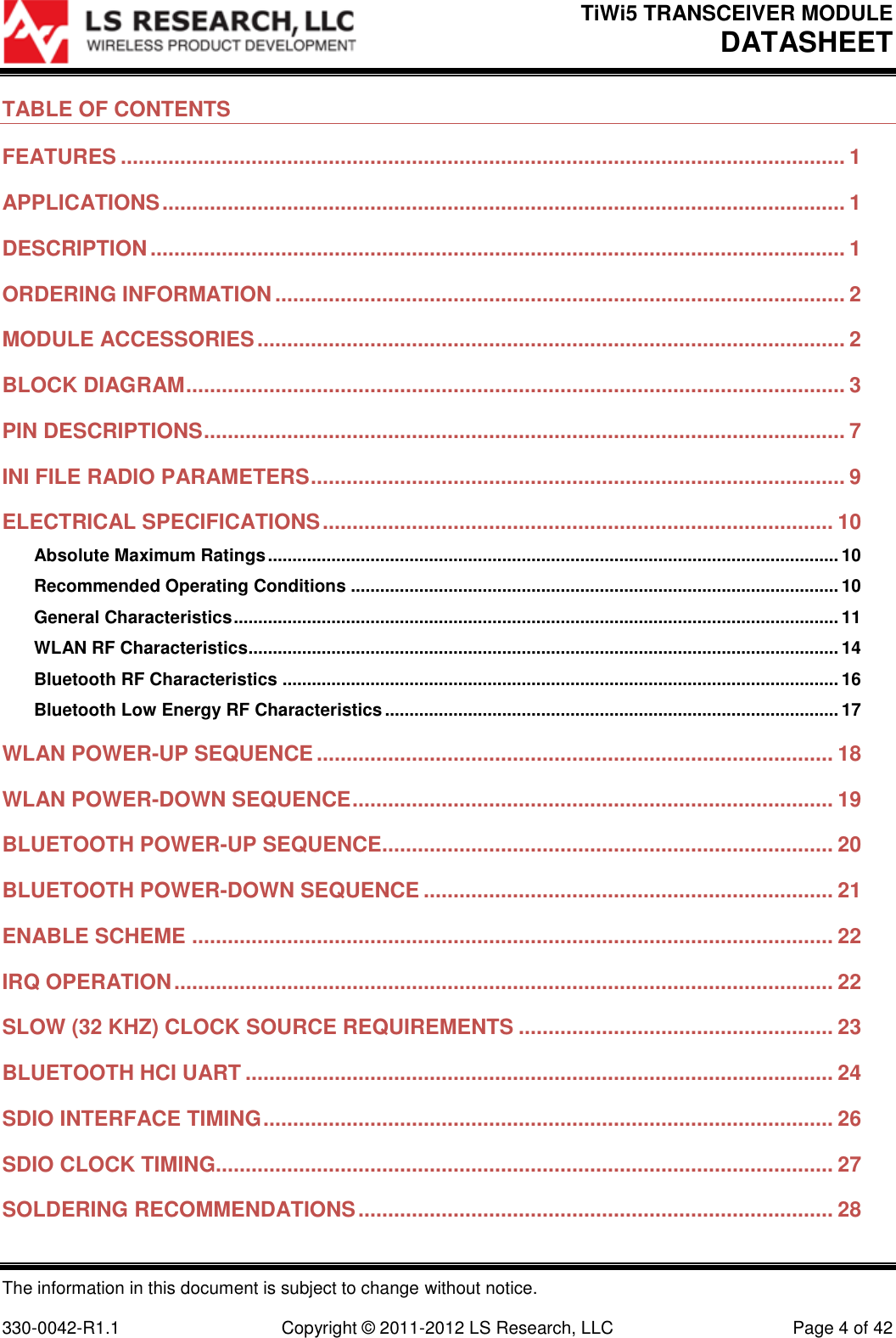
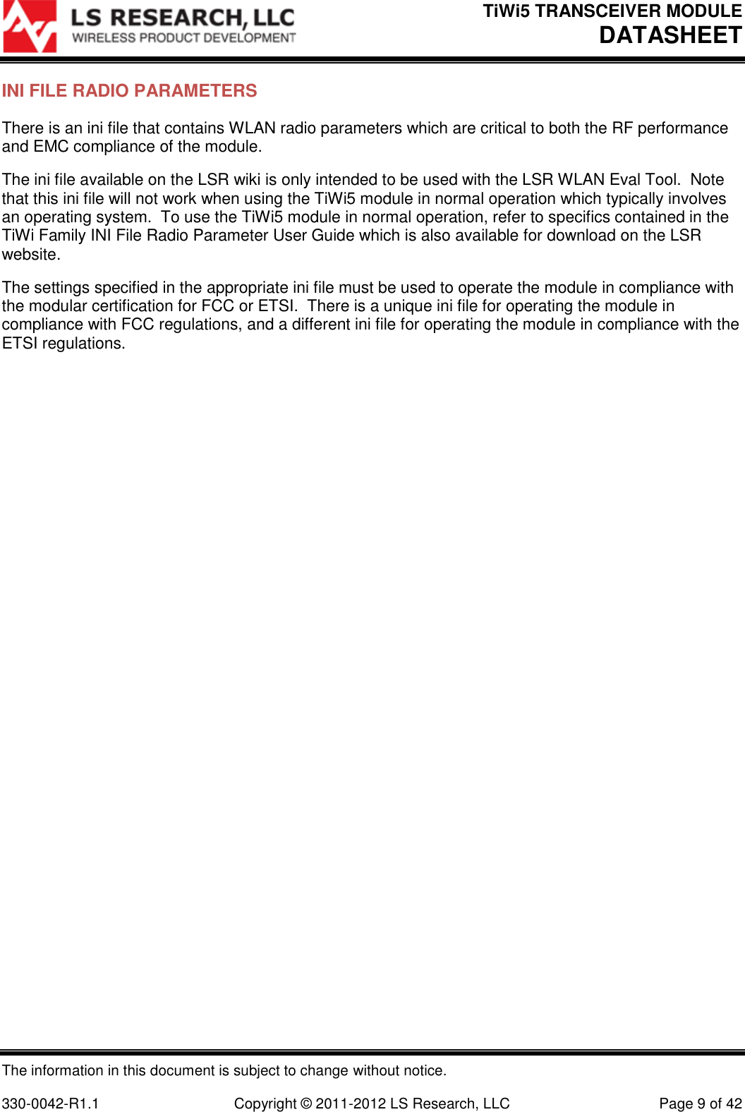
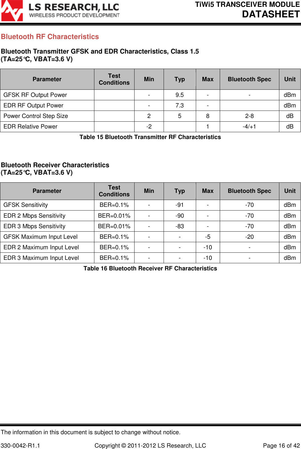
![TiWi5 TRANSCEIVER MODULE DATASHEET The information in this document is subject to change without notice. 330-0042-R1.1 Copyright © 2011-2012 LS Research, LLC Page 12 of 42 Power Consumption – WLAN 5 GHz Parameter Test Conditions Min Typ Max Unit OFDM 9 Mbps (802.11a) TX Current 5745 MHz, VBAT =3.6V, Tamb=+25°C Po=17.6 dBm, 9 Mbps OFDM L=1200 bytes, tdelay (idle)=4 S - 296 - mA OFDM 54 Mbps (802.11a) TX Current 5745 MHz, VBAT =3.6V, Tamb=+25°C Po=15.0 dBm, 54 Mbps OFDM L=1200 bytes, tdelay (idle)=4 S - 235 - mA MCS0 6.5 Mbps (802.11a) TX Current 5745 MHz, VBAT =3.6V, Tamb=+25°C Po=18.0 dBm, MCS0 OFDM L=1200 bytes, tdelay (idle)=4 S - 298 - mA MCS7 65 Mbps (802.11a) TX Current 5745 MHz, VBAT =3.6V, Tamb=+25°C Po=13.2 dBm, MCS7 OFDM L=1200 bytes, tdelay (idle)=4 S - 219 - mA 54/65 Mbps (802.11a/n) RX Current - 100 - mA Dynamic Mode [1] - <1.2 - mA [1] Total Current from VBAT for reception of Beacons with DTIM=1 TBTT=100 mS, Beacon duration 1.6ms, 1 Mbps beacon reception in Listen Mode. Table 8 5 GHz WLAN Power Consumption](https://usermanual.wiki/Laird-Connectivity/TIWI501.User-Manual/User-Guide-1763941-Page-12.png)
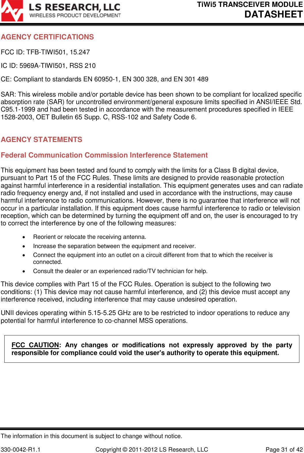
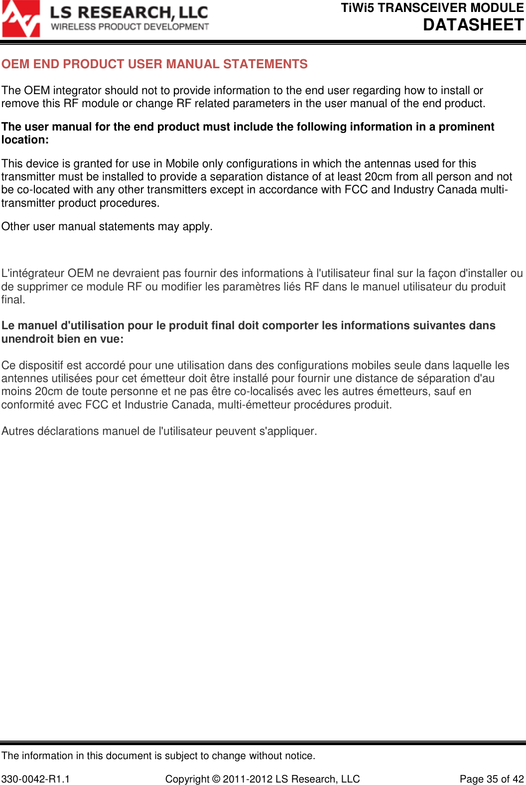
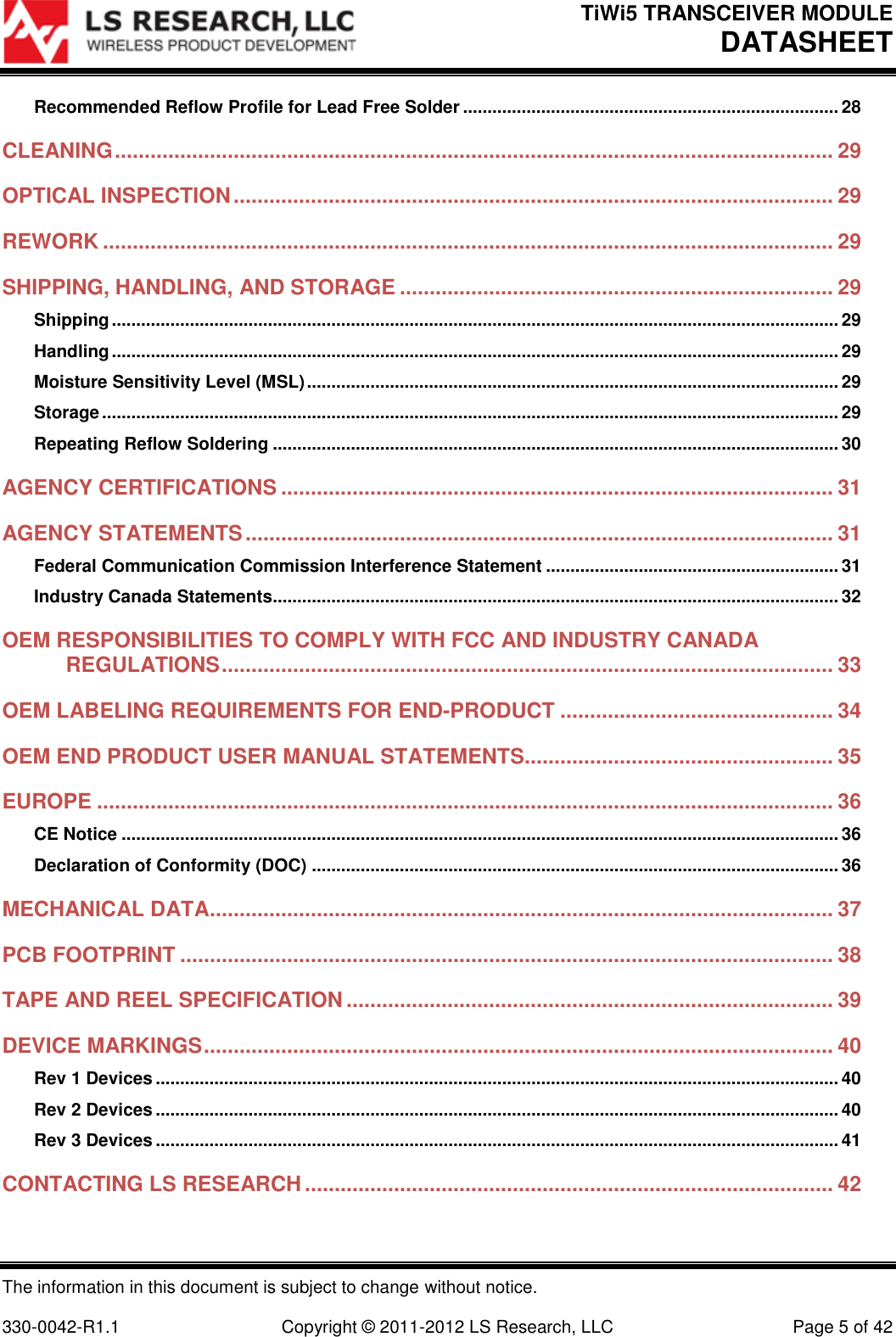
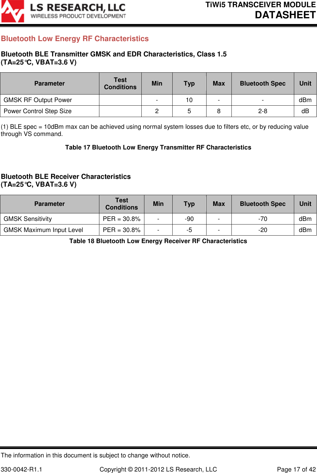
![TiWi5 TRANSCEIVER MODULE DATASHEET The information in this document is subject to change without notice. 330-0042-R1.1 Copyright © 2011-2012 LS Research, LLC Page 15 of 42 WLAN Receiver Characteristics 2.4 GHz (TA=25°C, VBAT=3.6 V) [1] Parameter Test Conditions Min Typ Max Unit 1 Mbps CCK (802.11b) RX Sensitivity 8% PER - -97 - dBm 11 Mbps CCK (802.11b) RX Sensitivity 8% PER - -88 - dBm 9 Mbps OFDM (802.11g) RX Sensitivity 10% PER - -89 - dBm 54 Mbps OFDM (802.11g) RX Sensitivity 10% PER - -74 - dBm 6.5 Mbps OFDM (802.11n) RX Sensitivity 10% PER - -89 - dBm 65 Mbps OFDM (802.11n) RX Sensitivity 10% PER - -72 - dBm 11 Mbps CCK (802.11b) RX Overload Level 8% PER - - -10 dBm 9 Mbps OFDM (802.11g) RX Overload Level 10% PER - - -17 dBm 54 Mbps OFDM (802.11g) RX Overload Level 10% PER - - -17 dBm 65 Mbps OFDM (802.11n) RX Overload Level 10% PER - - -17 dBm [1] Up to 2 dB degradation at Channel 13 for 11g/n modes and up to 2 dB degradation at Channel 14 for 11b/g/n modes. Table 13 2.4 GHz WLAN Receiver RF Characteristics WLAN Receiver Characteristics 5 GHz (TA=25°C, VBAT=3.6 V) [1] Parameter Test Conditions Min Typ Max Unit 9 Mbps (802.11a) RX Sensitivity 10% PER - -87 - dBm 54 Mbps (802.11a) RX Sensitivity 10% PER - -72 - dBm MCS0 6.5 Mbps (802.11a) RX Sensitivity 10% PER - -88 - dBm MCS7 65 Mbps (802.11a) RX Sensitivity 10% PER - -70 - dBm Max Input Level (3) OFDM (11a or 11n) <10% PER - - -17 dBm Table 14 5 GHz WLAN Receiver RF Characteristics](https://usermanual.wiki/Laird-Connectivity/TIWI501.User-Manual/User-Guide-1763941-Page-15.png)
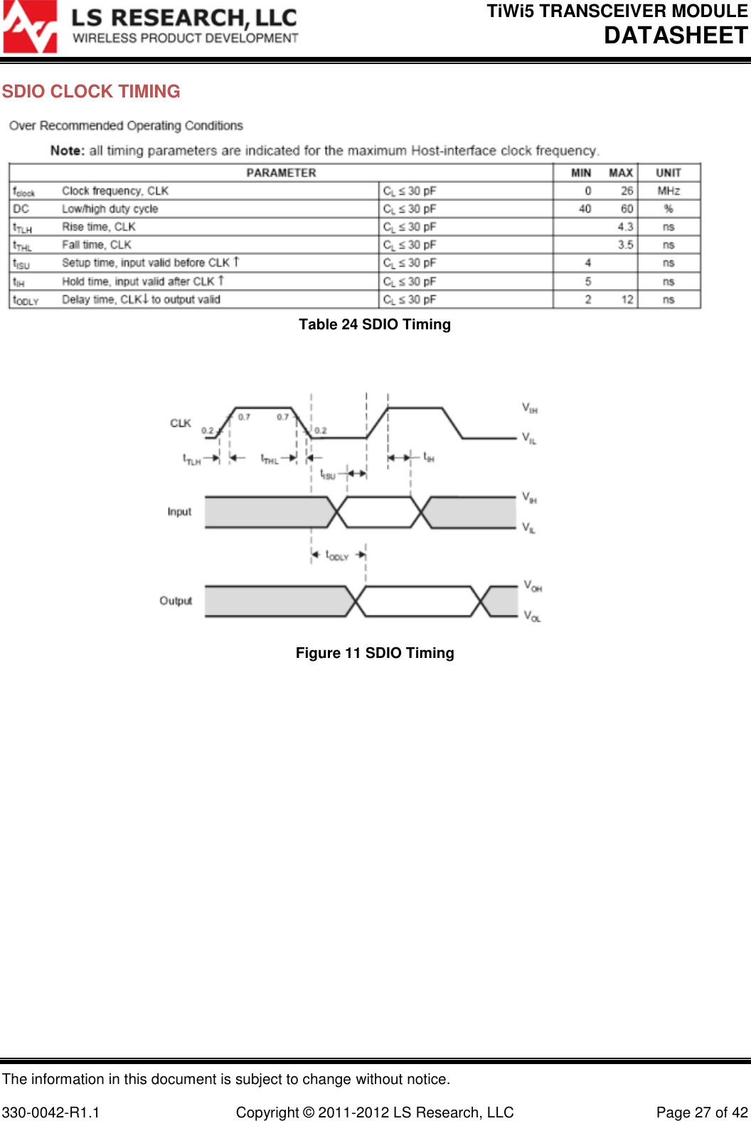
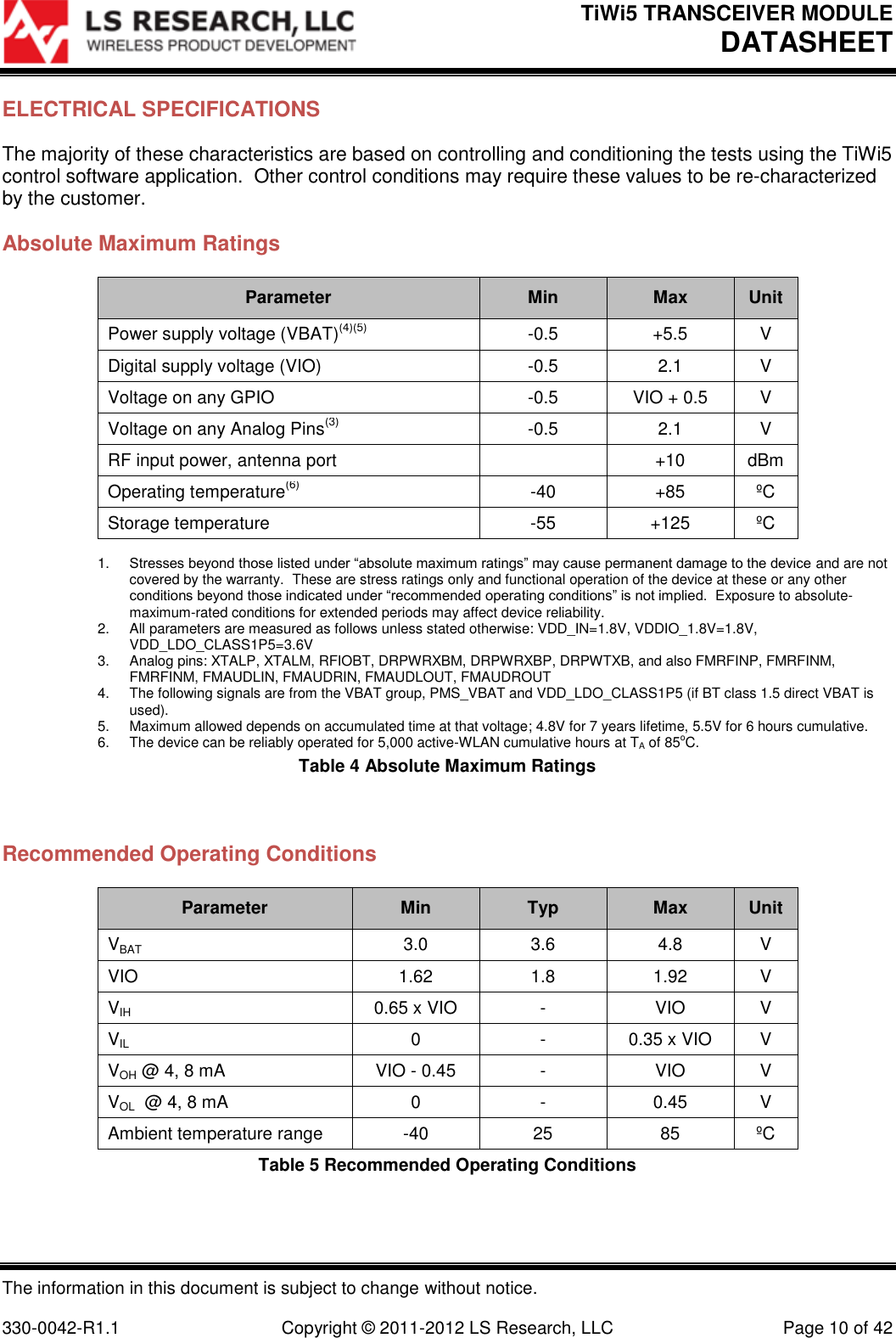
![TiWi5 TRANSCEIVER MODULE DATASHEET The information in this document is subject to change without notice. 330-0042-R1.1 Copyright © 2011-2012 LS Research, LLC Page 23 of 42 SLOW (32 KHZ) CLOCK SOURCE REQUIREMENTS The slow clock is always supplied from an external source. It is input on the SLOW_CLK pin, and can be a digital signal in the range of VIO only. For slow clock frequency and accuracy refer to Table 19. The external slow clock must be stable before the system exits from shut down mode. Parameter [1] Condition Symbol Min Typ Max Unit Input slow clock frequency 32768 Hz Input slow clock accuracy WLAN, BT +/-250 ppm Input transition time Tr/Tf – 10% to 90% Tr/Tf 100 ns Frequency input duty cycle 30 50 70 % Input voltage limits Square wave, DC coupled VIH 0.65 x VDDS VDDS Vpeak VIL 0 0.35 x VDDS Input impedance 1 MW Input capacitance 5 pF Rise and fall time 100 ns Phase noise 1 kHz -125 dBc/Hz [1] Slow clock is a fail safe input Table 19 Slow Clock Source Requirements](https://usermanual.wiki/Laird-Connectivity/TIWI501.User-Manual/User-Guide-1763941-Page-23.png)