Landis Gyr Technology NG0R1S2 Series 4 Single Board Radio User Manual 98 1138 QSG AD
Landis+Gyr Technology, Inc. Series 4 Single Board Radio 98 1138 QSG AD
UserManual.wiki
>
Landis Gyr Technology
>
NG0R1S2 User Manual
Manual
Navigation menu
Upload a User Manual
Namespaces
Wiki Guide
HTML
PDF
Info
Views
User Manual
Discussion / Help
Navigation

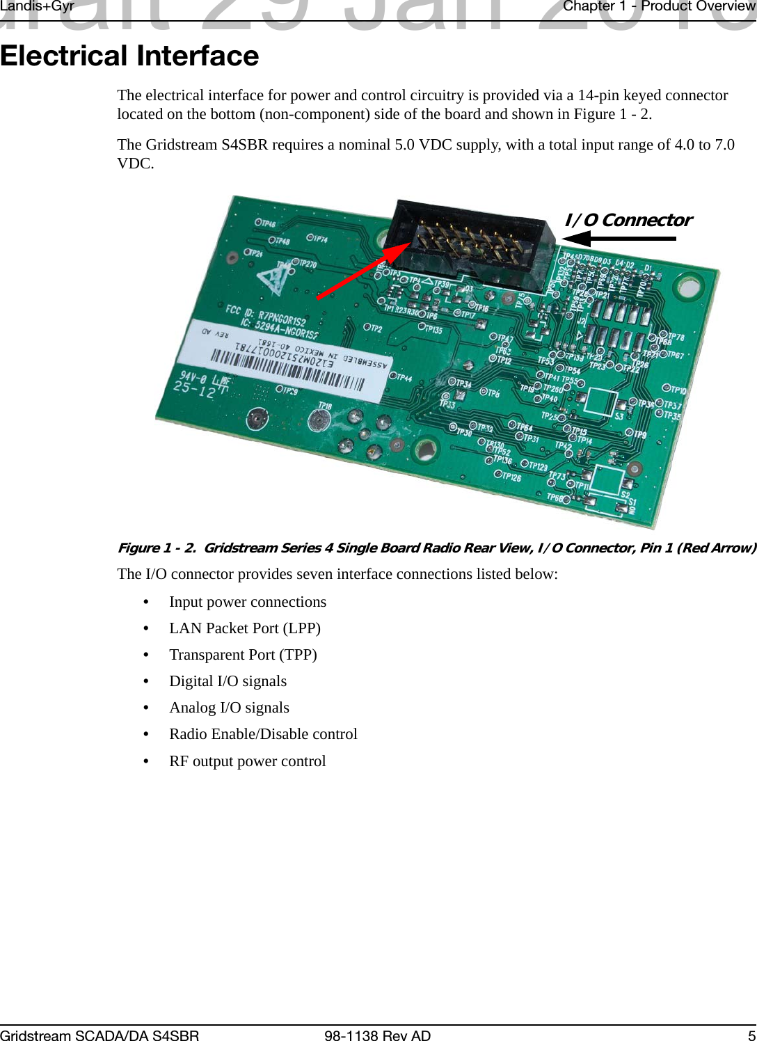
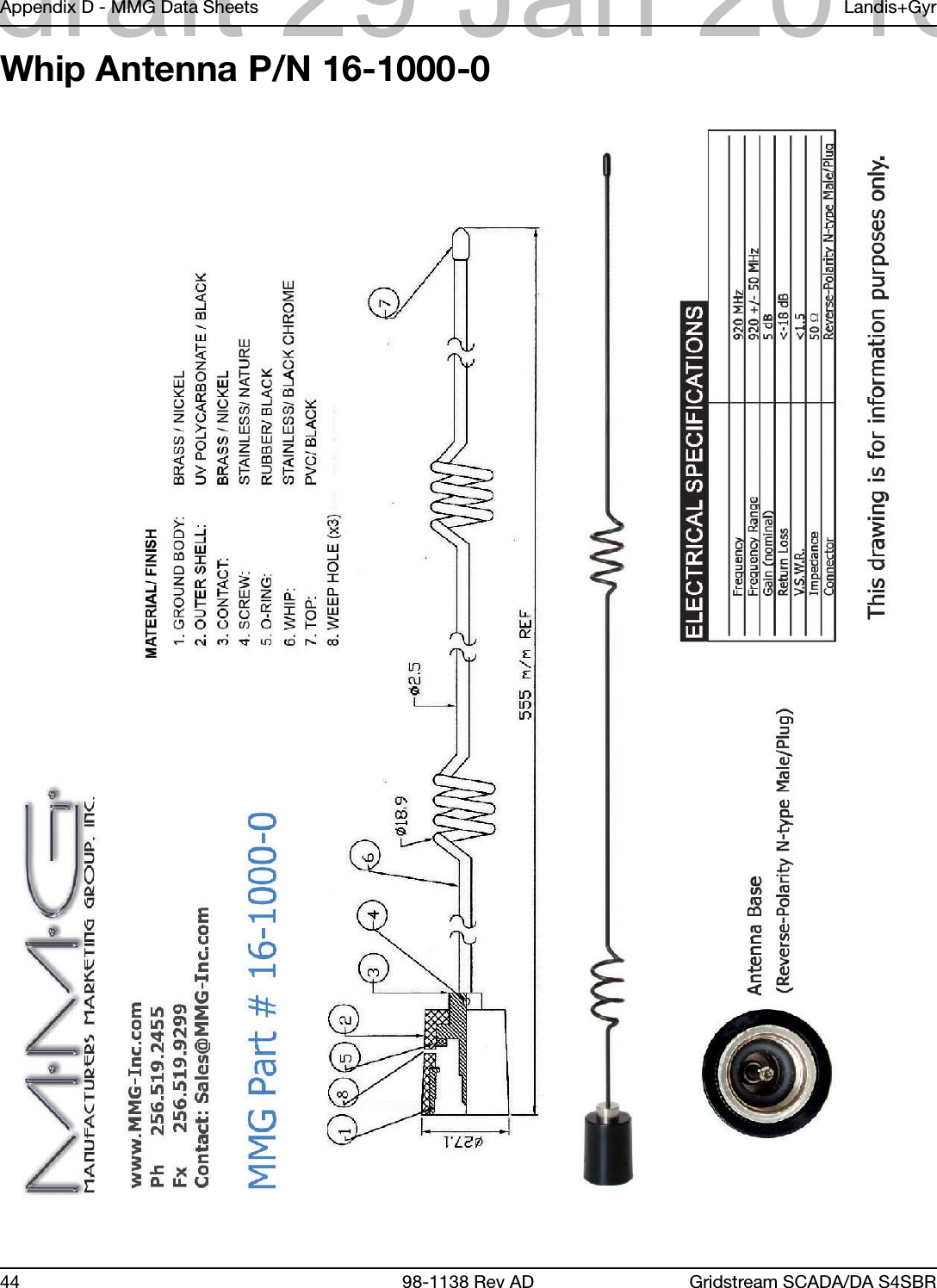
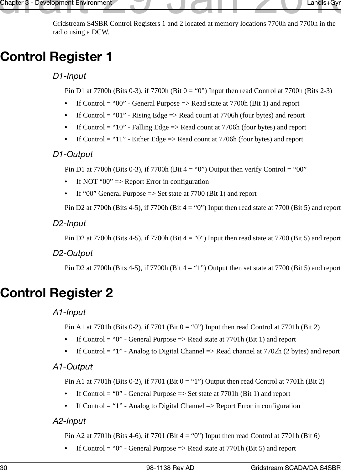
![Chapter 1 - Product Overview Landis+Gyr6 98-1138 Rev AD Gridstream SCADA/DA S4SBRPin FunctionsPin Outs for the connector as described below are designed to interface with developer OEM architecture. When pins are connected to non developer boards or when standard interfaces are required without use of the USB cable (P/N 19-2325, as shown in Figure 1 - 6), appropriate design constraints (power and logic level) must be adhered to (See “Gridstream SBR Logic” on page 30).Figure 1 - 3. Pinout Diagram (Rear View) For All Board Versions)Table 1 - 4. I/O Connector Pin Functions and Acceptable Voltage LevelsPin Number Name FunctionLogic Level Low (VDC)Logic Level High (VDC)1 VIN Main supply for the board. 04.0 ~ 7.0Nominal = 5.02 LPP TX This pin is an output from the device for connecting to RadioShop via the LAN Packet Port (LPP) interface. 0 ~ 0.5 2.8 ~ 3.43 LPP RX This pin is an input to the device for connecting to RadioShop via the LAN Packet Port (LPP) interface. 0 ~ 0.6 2.6 ~ 3.44 DIGITAL_IO1 A general purpose Digital Input / Output Pin. The application-specific DCW can use this pin as desired. 0 ~ 0.6 2.6 ~ 3.45ANALOG_IN1An input to the device’s A/D converter. The application-specific DCW can read the voltage on this pin. Note: This pin may be configured as a Digital I/O, if desired.0 ~ 2.56 and 7 GND Common ground for both power and communications. These two pins are tied together on the device. 008 LOW_RF_POWER Digital input used to select Low-Power Mode, an RF output power reduction to 100 mW [20 dBm]. ground 3.3V max9 PWR_DN Digital input used to completely shut down the device. ground 2.8 ~ 5V max10 ANALOG_IN2An input to the device’s A/D converter. The application-specific DCW can read the voltage on this pin. Note: This pin may be configured as a Digital I/O, if desired.0 ~ 2.511 DIGITAL_IO2 A general purpose Digital Input / Output Pin. The application-specific DCW can use this pin as desired. 0 ~ 0.6 2.6 ~ 3.412 TPP RX This pin is an input to the Transparent Port (TPP) device. 0 ~ 0.6 2.6 ~ 3.413 TPP TX This pin is an output from the Transparent Port (TPP) device. 0 ~ 0.5 2.8 ~ 3.414 3.3V_Logic_supply 3.3V Supply for logic level shifting. Pin is current limited to 300μA ≈3.3 draft 29 Jan 2013](https://usermanual.wiki/Landis-Gyr-Technology/NG0R1S2/User-Guide-1890219-Page-10.png)
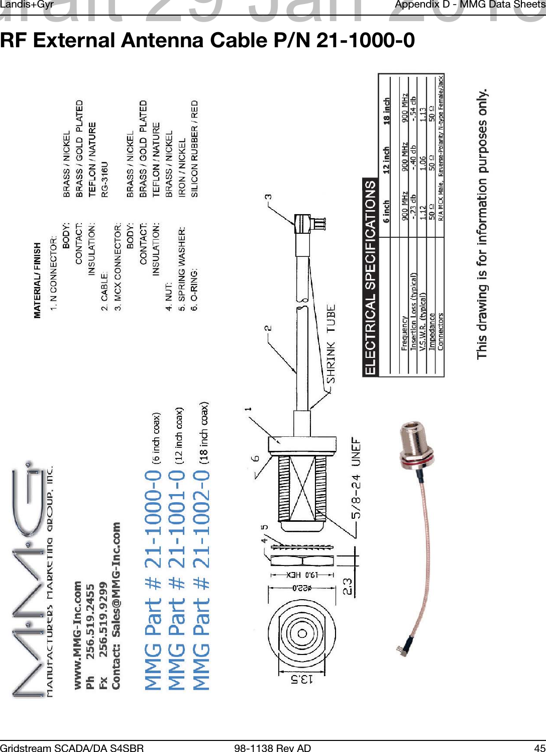
![Landis+Gyr Chapter 1 - Product OverviewGridstream SCADA/DA S4SBR 98-1138 Rev AD 7Pin 1 (VIN)This pin must be supplied with DC voltage between 4.0 and 7.0 VDC with 5.0 VDC considered nominal.The input voltage is linearly regulated on the board. While the linear regulation can remove some noise, Power Supply Rejection Ratio (PSRR) varies with frequency. If the power source is particularly noisy, filtering may be required. Landis+Gyr engineering can assist in defining radio tests to determine if power supply noise is affecting radio performance.The input voltage must be maintained between 4.0 VDC and 7.0 VDC during operation. The on-board electronics include fast-acting reset circuitry. If the voltage drops below 4.0 VDC, even transiently, the system will reboot once the voltage returns to normal range. If the voltage rises above 7.0 VDC, even transiently, the voltage-sensitive components could be damaged.Upon power up, the on-board processor and voltage regulator requires the supply voltage to have a minimum of 0.05 V/msec slew rate - which implies rising from a logic 0 to a logic 1 in no less than 66 msec. Power consumption during normal receive mode is typically 41 mA. Current consumption during 100 mW transmit mode is 250 mA, 440 mA during 450 mW transmit mode, and 520 mA during 600 mW transmit mode.During the first 30 minutes after initial power-on or after an extended outage, the on-board super-capacitor will be charging. During this time, the total input current to the device will increase by 80 mA. SeeTable 1 - 1, "Series 4 Gridstream S4SBR General Electrical Specifications," for additional details.The Gridstream S4SBR uses a frequency-hopping sequence transmission and, while typically rare, transmissions can be as long as 400 mS in duration, and can theoretically sustain at a 45% duty cycle on a single channel.Figure 1 - 4. Single-channel Worst-Case Current Consumption ProfileFigure 1 - 5. Typical Current Consumption ProfileTime [mS]55255~ 400[mS]~ 500[mS]Iin [mA]Time [mS]25175~ 250[mS]OccasionalPacketsIin [mA]draft 29 Jan 2013](https://usermanual.wiki/Landis-Gyr-Technology/NG0R1S2/User-Guide-1890219-Page-11.png)
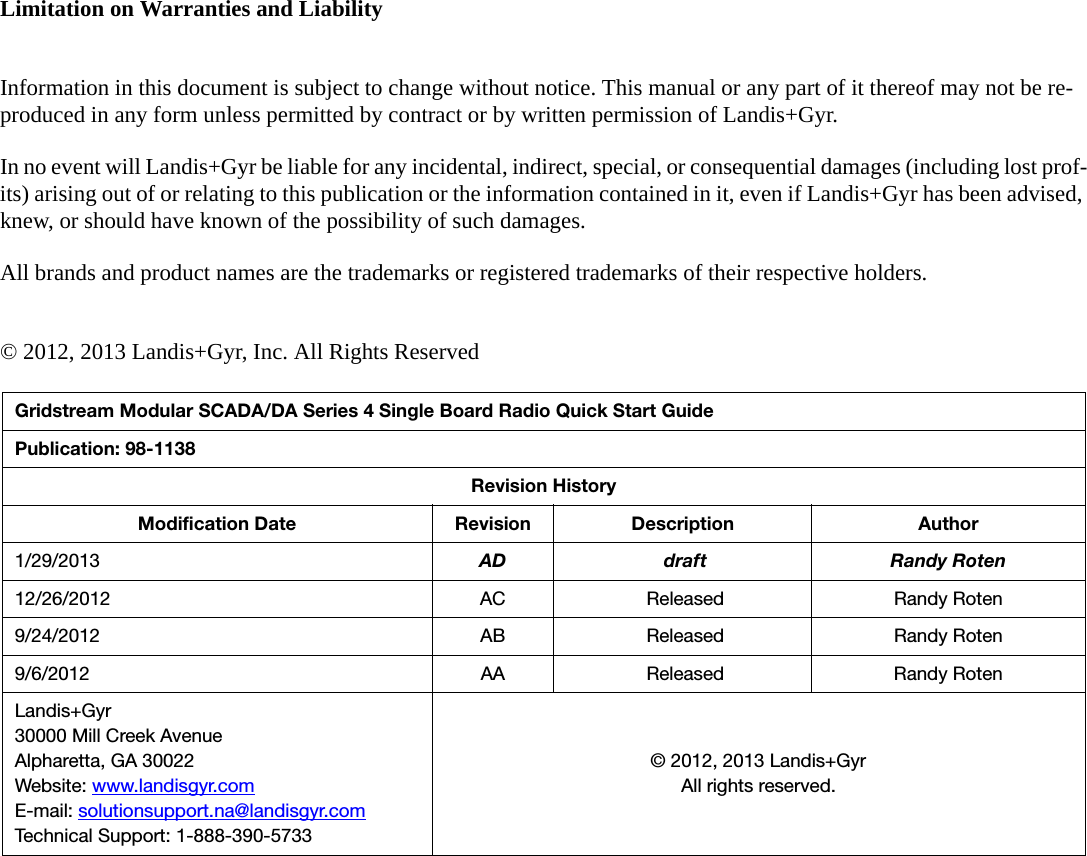
![Chapter 1 - Product Overview Landis+Gyr8 98-1138 Rev AD Gridstream SCADA/DA S4SBRPin 2 (LPP TX) and Pin 3 (LPP RX)These pins are used to interface with the device's LAN Packet Port. These pins are driven at TTL level supply, 2.5 VDC.Baud rates on this port default to 9,600 bps but, using RadioShop, are configurable from 1,200 bps to 115,200 bps.To reduce chances of electrical damage, a 10Kohm series resistor is placed in-series with the pin which limits the drive current capability of this pin. Stray physical capacitance on this circuit should be kept below 250[pF].NOTE: These pins should NOT be directly connected to an RS-232 interface on a computer. Where such a connection is necessary, the developer must connect to the unit through an externally-powered TTL to RS-232 VDC converter, NOT via the pins or the RS-232 connection on the computer.Pin 4 (DIGITAL_IO1) and Pin 11 (DIGITAL_IO2)These pins are general purpose digital I/O lines and are driven at TTL supply levels.If not used, they should not be left unconnected and should be held low by connecting the pin to a common ground.If used, these pins must be driven to a valid logic high or low and not left at intermediate voltages as this will result in indeterminate logic values and may damage the device.draft 29 Jan 2013](https://usermanual.wiki/Landis-Gyr-Technology/NG0R1S2/User-Guide-1890219-Page-12.png)
![Chapter 1 - Product Overview Landis+Gyr10 98-1138 Rev AD Gridstream SCADA/DA S4SBRA logic low (pin connected to ground) reduces the RF output power level to approximately 100 mW for use in environments where high RF output power is not required or only low input power is available to the device. When the USB cable is used to power the board, the pin is automatically brought low. This pin is a digital input, driven internally at TTL supply level.This pin must be left not connected or pulled low to ground as intermediate voltages will result in indeterminate conditions and may damage the device.Pin 9 (PWR_DN)This pin is used to enable or disable the Gridstream S4SBR. It is a digital input and must be driven to a valid logic high (5.0 VDC) or low (GND), since intermediate voltages will result in indeterminate logic values and may damage the device.NOTE: When the Pin 9 power-off command is asserted on super-capacitor units, the unit will remain operational for a few minutes as the super-capacitor voltage bleeds off. Once Pin 9 power-off command is asserted on units without the super-capacitor, the units will turn off immediately.•A logic high (5VDC) provides power to the device.•A logic low (GND) turns off the device.Prior to turning off the device, all interface signals must be driven low and logic voltage removed. This includes all TTL logic lines, digital and analog I/O lines.When the device is turned off with this pin, total current consumption will be less than 100µA.NOTE: When the board is not in use, voltage should not be applied to any interface. Applied voltage may damage the device as destructive latch-up may occur.Pin 12 (TPP RX) and Pin 13 (TPP TX)These pins are used to interface with the device's Transparent Port. These pins are driven at TTL supply level.Baud rates on this port default to 9,600 bps but, using RadioShop, are configurable from 300 bps to 115,200 bps.To reduce chances of electrical damage, a 1Kohm series resistor is placed in-series with the pin which limits the drive current capability of this pin.Stray physical capacitance on this circuit should be kept below 250[pF].NOTE: These pins should NOT be directly connected to an RS-232 interface on a computer. Where such a connection is necessary, the developer must purchase a TTL to RS-232 VDC converter which is powered external and NOT via the pins or the RS-232 connection on the computer.draft 29 Jan 2013](https://usermanual.wiki/Landis-Gyr-Technology/NG0R1S2/User-Guide-1890219-Page-14.png)
![Chapter 1 - Product Overview Landis+Gyr14 98-1138 Rev AD Gridstream SCADA/DA S4SBRAdditional SpecificationsTable 1 - 7. Additional SpecificationsCategory Specification Value(s) or Range(s)NetworkingNumber of Channels 240 (narrow channel mode), 86 (wide channel mode)Channel Spacing 100 KHz (narrow channel mode), 300 KHz (wide channel mode)Modulation Type 2-FSKRF Baud Rate 9.6, 19.2, 38.4, 115.2 kbpsFCC Operation Certification Part 15.247Spreading Technique Frequency HoppingHopping Technique Pseudo Random AsynchronousHopping Patterns 65,536 (Unique per network)Network Address Latitude / Longitude CoordinatesTurn-Around Time 100[uS] maxProgrammingProgramming Language Device Control Word (DCW)Radio Firmware Version 5.72 laterDataLAN Packet Port (LPP)Serial Interface, DCW adjustable per specs belowData Rate - 9.6, 19.2, 38.4, 115.2 kbpsTransparent Port (TPP)Serial Interface, DCW adjustable per specs belowData Rate - 9.6, 19.2, 38.4, 115.2 kbpsSerial Interface TTLParity Odd, Even, or NoneData bits 7 or 8Stop bits 1 or 2Duplex FullProtocol Any asynchronous byte-oriented protocolEnvironmentalOperating Temperature -40°C to +85°CStorage Temperature -40°C to +85°CHumidity 85C, 95% RHMechanical SizeOn-board Antenna 3.43”L x 2.275”W x 0.65”H (0.96”H w- Super Cap)External Antenna 3.43”L x 1.65”W x 0.65”H (0.96”H w- Super Cap)draft 29 Jan 2013](https://usermanual.wiki/Landis-Gyr-Technology/NG0R1S2/User-Guide-1890219-Page-18.png)

![Chapter 3 - Development Environment Landis+Gyr32 98-1138 Rev AD Gridstream SCADA/DA S4SBRAnalog Input FunctionalityThis device provides two general purpose analog inputs. These are filtered and connected to a 10-bit A/D converter.NOTE: The voltage reference for this A/D converter is 2.5 VDC +/- 60[mVDC] across the operating temperature range.This A/D converter has the following specifications:NOTE: The actual sampling time is 0.25 μS and the conversion time is 2.75 μS, but the rate at which signals on these inputs can be sampled in-practice is limited by the DCW execution. It is recommended that these channels be used only for DC voltage measurement, and that the sampling rate can not exceed 100 mS.The register below can be used to control either of the two general purpose Analog pins (A1 & A2) located at memory location 7701 (hex).Table 3 - 2. A/D Converter SpecificationsA/D characteristic SpecificationResolution 10 bitINL +/-5 LSBAbsolute Accuracy +/-5 LSBDNL +/-1 LSBOffset Error +/-3 LSBGain Error +/-3 LSBTable 3 - 3. Control Register 2Bit Feature Description Dflt.0Pin A1 Direction 0: Input1: Output 01 Pin A1 StateWhen A1, bit 0 is "0" and bit 2 is "0", then bit 1 returns current state as "0" or "1".When A1, bit 0 is "0" and bit 2 is "1", then read location 7702-7703 which returns the Hex value of the sampled voltage between 0-2.5 VDC.When A1, bit 0 is "1", then the value of bit 1 can be set.02Pin A1 Control 0: General Purpose I/O1: Analog to Digital Channel (Bit 0 = "0" only) 03 Reserved Not Used 04Pin A2 Direction 0: Input1: Output 0draft 29 Jan 2013](https://usermanual.wiki/Landis-Gyr-Technology/NG0R1S2/User-Guide-1890219-Page-36.png)
![Landis+Gyr Chapter 3 - Development EnvironmentGridstream SCADA/DA S4SBR 98-1138 Rev AD 33Memory LocationINTRODUCTION INFORMATION[7702-7703h] Analog to Digital Channel A1.When A1 is set to "Analog to Digital" (Bit 2) this location will contain a 10-bit reading. The scale on this board is from 0 to 2.5 volts. Voltages greater than 2.5 VDC will be reported as 2.5 VDC.[7704-7705h] Analog to Digital Channel A2.When A2 is set to “Analog to Digital” (Bit 6) this location will contain a 10-bit reading. The scale on this board is from 0 to 2.5 volts. Voltages greater than 2.5 VDC will be reported as 2.5 VDC.[7706-7709h] D1 Interrupt Counter.If D1 is configured as an interrupt (Bit 2-3) then this location will count the number of interrupts that have been detected.NOTE: The interrupt counter is cleared each time interrupts are enabled.5 Pin A2 StateWhen A2, bit 4 is "0" and bit 6 is "0", then bit 5 returns current state as "0" or "1".When A2, bit 4 is "0" and bit 6 is "1", then read location 7704-7705 which returns the Hex value of the sampled voltage between 0-2.5 VDC.When A2, bit 4 is "1", then the value of bit 5 can be set.06Pin A2 Control 0: General Purpose I/O1: Analog to Digital Channel (Bit 0 = "0" only) 07 Reserved Not Used 0Table 3 - 3. Control Register 2Bit Feature Description Dflt.draft 29 Jan 2013](https://usermanual.wiki/Landis-Gyr-Technology/NG0R1S2/User-Guide-1890219-Page-37.png)