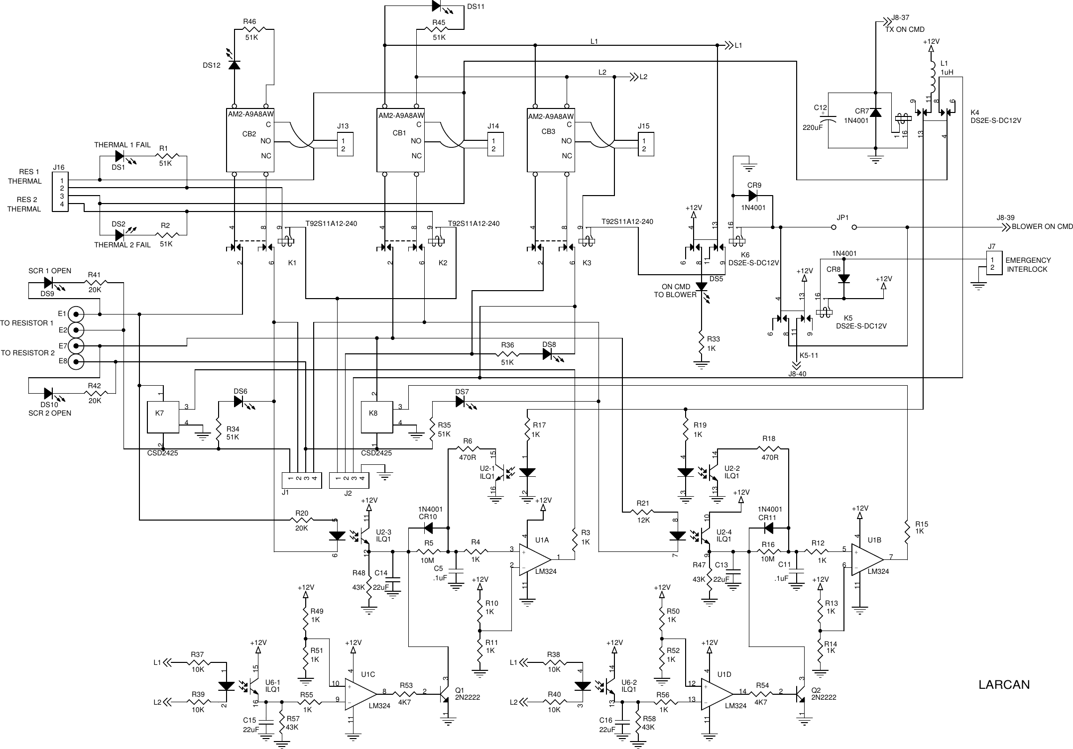
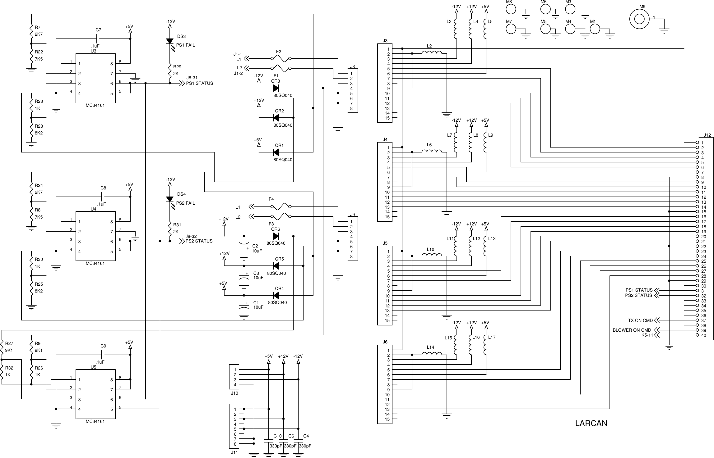
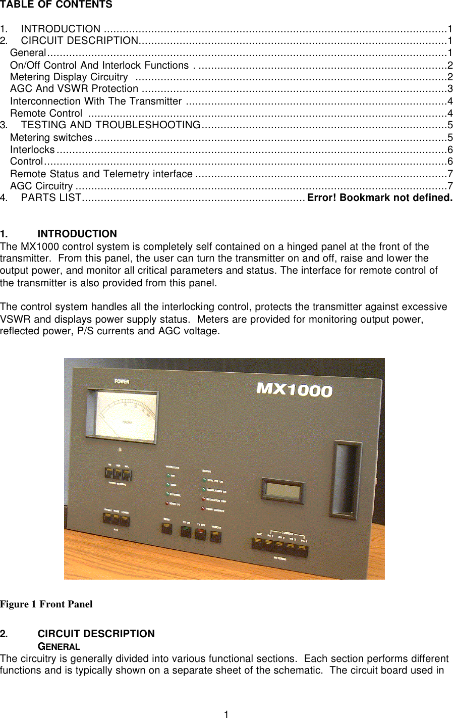
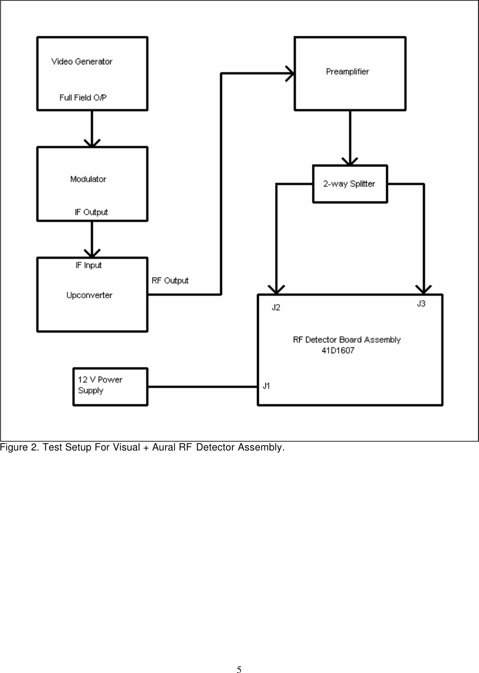
Larcan MX1000U 1000 Watt UHF Translator User Manual mx1ku
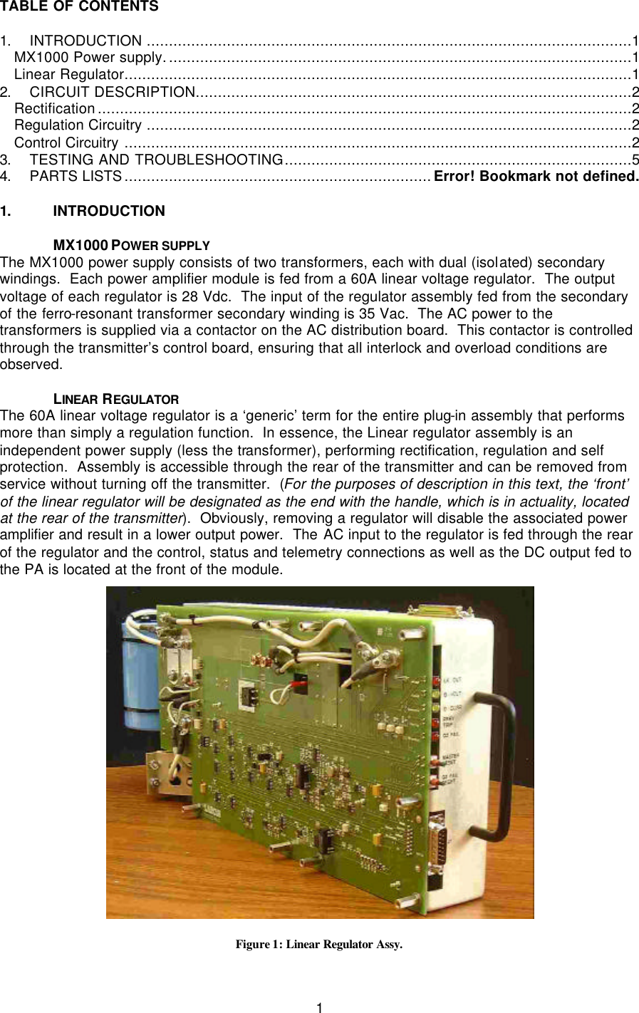
Larcan Inc 1000 Watt UHF Translator mx1ku
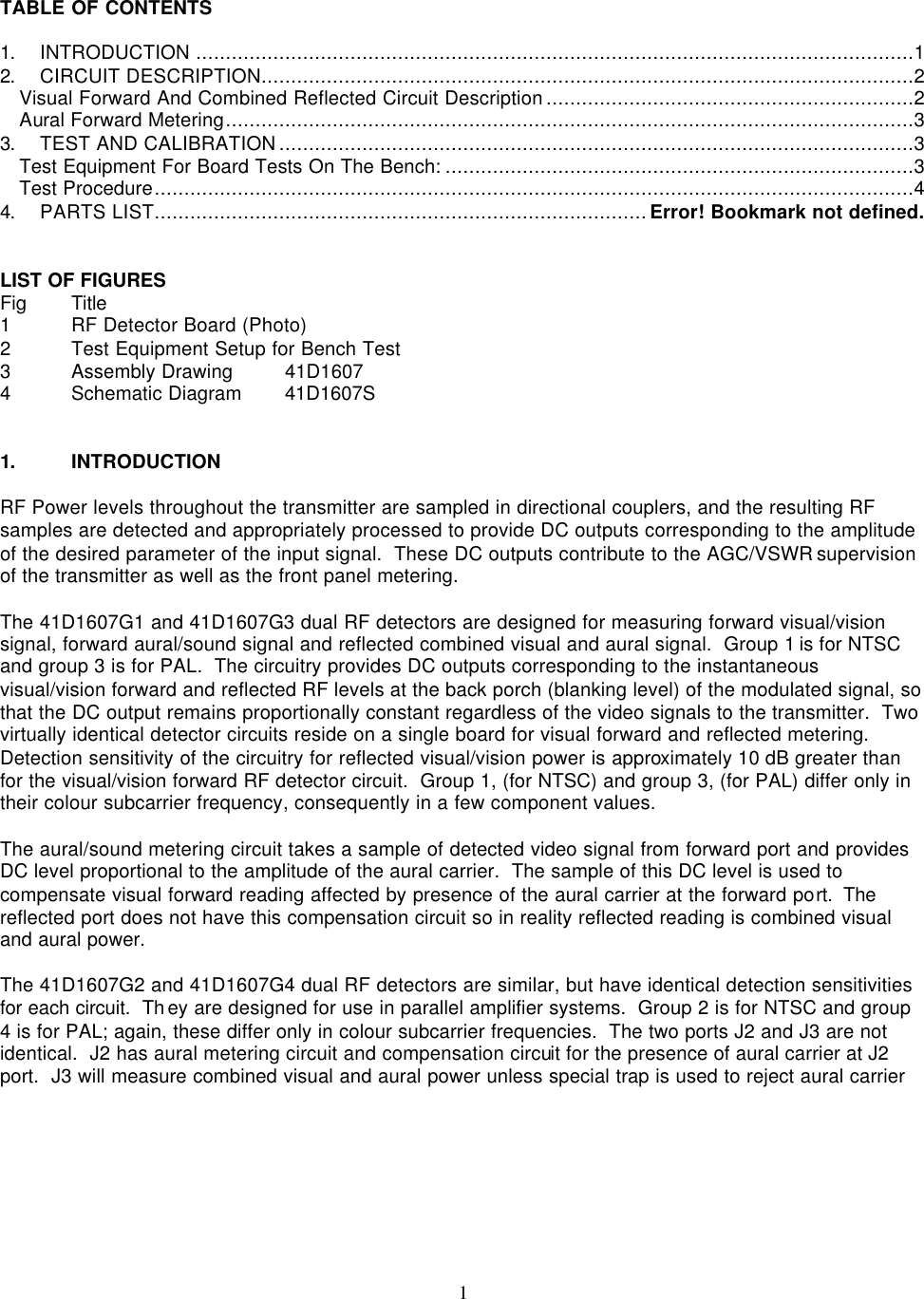
UserManual.wiki
>
Larcan
>
MX1000U User Manual
Users Manual
Navigation menu
Upload a User Manual
Namespaces
Wiki Guide
HTML
PDF
Info
Views
User Manual
Discussion / Help
Navigation
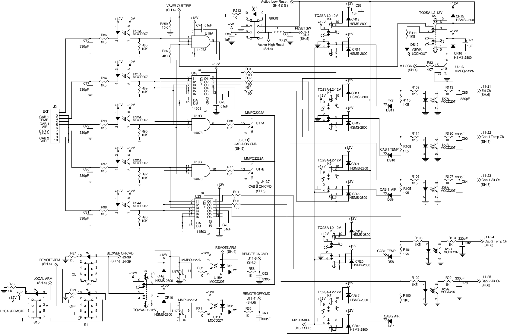
![4 TEST EQUIPMENT REQUIRED • 12 V power supply • UHF preamplifier (approx 200mWo/p). • Video Generator. • Modulator. • UHFUpconverter. • Oscilloscope. • Spectrum Analyzer. • VHF / UHF Two Way Splitter. requires an external amplifier, and the exciter aural output may be used as an unmodulated source if required (A LARCAN exciter visual/vision section can not deliver unmodulated RF). TEST PROCEDURE For test setup, see Figure 2. 1. Connect board under test to power supply. Apply ground on pin 7 & 8 of J2 and apply +12v (± 0.2 V) to pins 3 & 4. Do not apply RF to J2 and J3 yet. 2. Adjust R111 max CW. 3. Adjust R10 to get a min voltage at Ul0-1 (TP9). 4. Check the voltage between U10-2 and U10-3. It should be no more than 10 mV. 5. Adjust R42 to get a minimum voltage at U6-7 (TP10). 6. Check the voltage between U6-6 and U6-5. It should be no more than 10 mV. 7. Set R104 in mid position. 8. Apply staircase modulated RF signal from UHF upconverter to J2 and J3 through splitter according to Table 1. The signal should include aural carrier 10 dB lower than visual sync peak. Check this level on the spectrum analyzer. Note: Make sure to set spectrum analyzer resolution RBW to 300 kHz to see sync peak level. Assembly Group G1/G3 G2/G4 Connector J2 J3 J2 J3 Visual Peak Signal [dBm] 23 13 20 20 TABLE 1. 9 Adjust R104 for 7.5 ± 0.5 V at TP8. 10 Adjust R107 for 4V at TP3. 11 Adjust R28 so that CR2 lights up. 12 Adjust R57 so that CR4 lights up. 13 Using the oscilloscope, check that there are positive 12V pulses at TP4 and TP5. 14 Check DC voltage at TP9. 15 VTP9 should be within 4.5V to 9.5V. 16 Check DC voltage at TP10. 17 VTP1O should be within 4.5V to 9.5V. 18 Turn off the aural carrier. 19 Adjust R13for4VatTP1. 20 Turn on the aural carrier. 21 Adjust R111 for4V at TPl. 22 Repeat steps 12 and 13 until voltage at TP1 stays the same with and without aural carrier. 23 Adjust R43 for 4 V at TP2 with aural carrier on.](https://usermanual.wiki/Larcan/MX1000U/User-Guide-444106-Page-8.png)
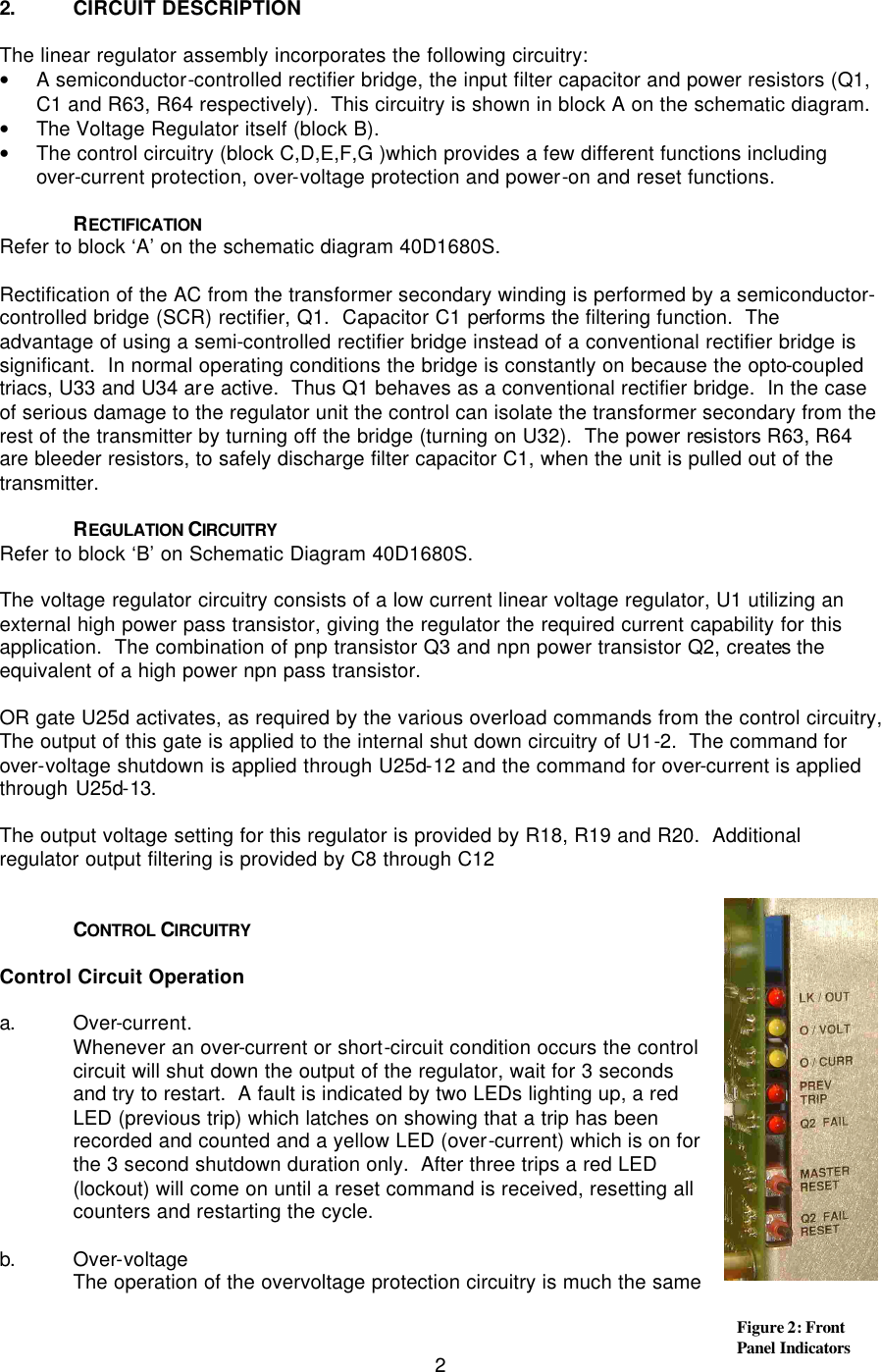
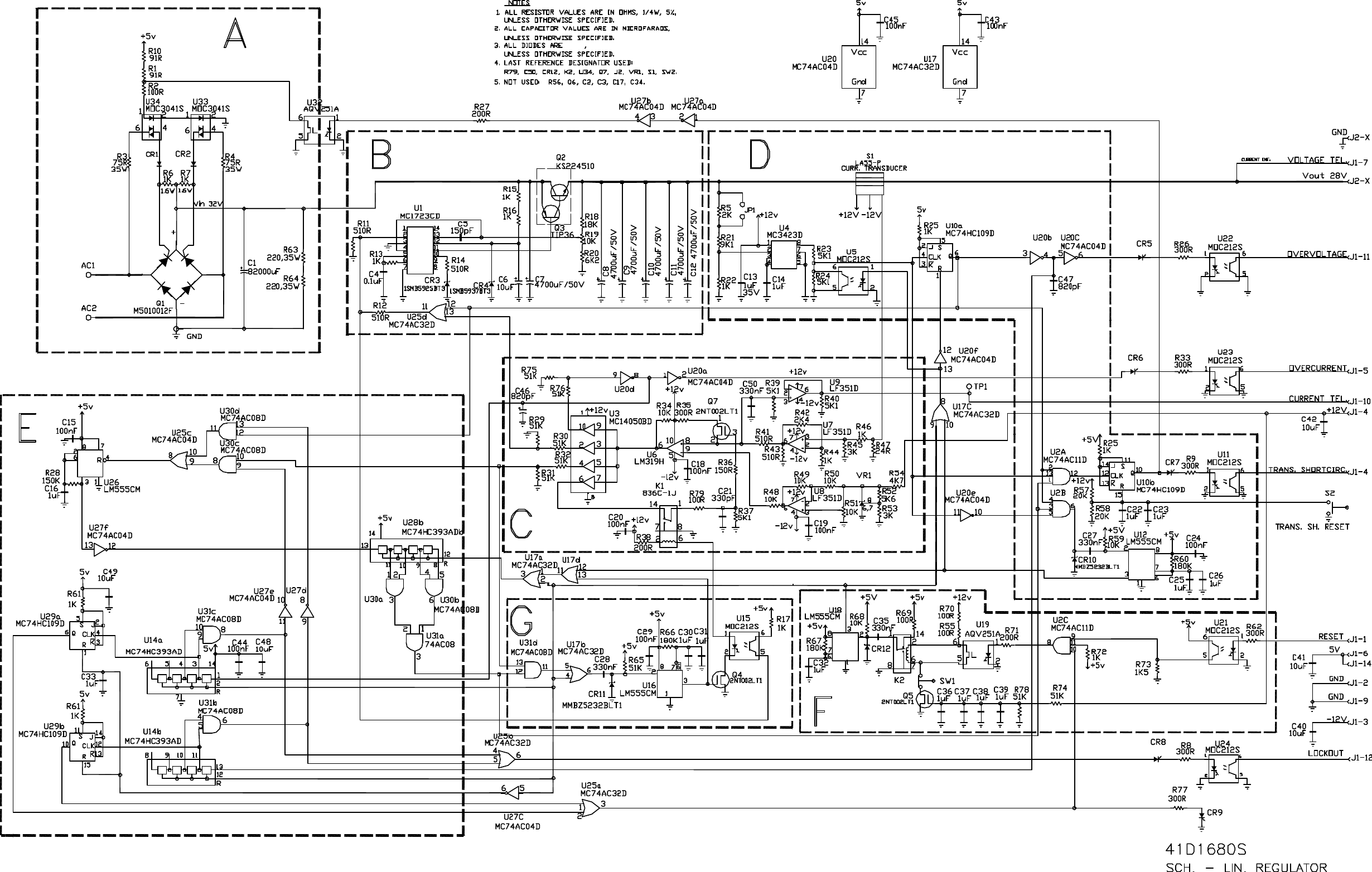
![3 as that of the overcurrent circuitry with a couple of exceptions. One of the common causes of failure in a series linear regulator is the short circuit of the series pass transistor. Once the pass transistor has shorted, there is no way to shut down the regulator output (to prevent over-voltage damage to the power amplifiers), hence the SCR bridge that effectively disconnects the entire regulator from the transformer secondary. When the over-voltage protection circuitry detects an over-voltage condition the circuit shuts down the output of the regulator for 3 seconds and then tries to restart the regulator. The fault is shown by two LEDs lighting up, the red LED (previous trip) which latches on showing that a trip has been recorded and counted and a yellow LED (over-voltage) which is on for the 3 second shutdown duration only. After three trips a red LED (lockout) will come on until a reset command is received, resetting all counters and restarting the cycle. In the event that the series pass transistor short circuits, turning off the regulator IC will have no effect. In this case, additional control circuitry will shut down the rectifier bridge isolating the regulator. A red LED (Q2 short-circuit) comes on. A local reset switch for this circuitry is available for restarting the regulator (if the pass transistor is indeed short circuited the circuitry will again shut down the regulator showing the same fault condition). In this case the regulator must be serviced and Q2 replaced. Until the necessary steps are taken to do this, the damaged regulator is safely isolated from the rest of the transmitter. c. Power ON Reset and Master Reset The regulator assembly utilizes control voltages supplied by the transmitter control power supplies. These are supplied via a connector on the front of the regulator module. In the event that these ‘auxiliary’ voltages are removed from the circuit the regulator control circuit shuts down the rectifier bridge, isolating the regulator. This situation could occur if either the auxiliary power supply fails or if the 15 pin control connector is disconnected leaving the unit without the auxiliary voltages. When the voltages are reapplied, the circuitry sends a power-on reset pulse, setting all counters and protection circuits back to original conditions. The same effect occurs when the master reset switch is pressed and released. Over-current protection (refer to block C on schematic diagram 41D1680S) Along with current transducer S1, block C on the schematic contains the over-current protection. The current information from S1 is amplified and compared to a threshold determined by the setting of R51. When the current information reaches the threshold level, the output of comparator U6 goes high (0 to 10V). U3 is a buffer amplifier that is used to distribute the over-current status to various other circuits within the regulator (see table) Whenever an over-current event happens, the comparator output toggles (U6-6) and the positive level through U3 (pin 6) is transferred through the closed contacts of K1 to the gate of Q7. Q7 turns on and R35, R41 and R43 form a voltage divider latching U6 into the ‘tripped’ state. When a reset command is issued relay K1 is activated, the gate of Q7 discharged and the circuit comes back to its original state. Over-Voltage Protection (refer to Block D on Schematic diagram 41D1680S) Over-voltage condition is sensed by U4. This is a programmable voltage sensor. The threshold over-voltage reference is set by the voltage divider consisting of R5, R21 and R22 (the threshold is set by the following formula: V= 2.6 [1+ (R5+R21)/ R22] ). An over-voltage condition causes Pin (U3) Output function pin 10 front panel status LED (over-current ) and via inverter U20d to over-current event counter U14a. pin 2 activates the OR gate U25d shuting down the regulator. pin 4 starts the timing circuitry (see block E ). pin 6 activates the locking circuitry.](https://usermanual.wiki/Larcan/MX1000U/User-Guide-444106-Page-28.png)