MX30V Manual
PUBLICATION TSM 20-332
TECHNICAL MANUAL
30 WATT VHF AMPLIFIER
FOR MX30V SERIES
TV TRANSMITTER/TRANSLATOR
LARCAN INC.
228 AMBASSADOR DRIVE
MISSISSAUGA, ONTARIO
CANADA L5T 2J2
PHONE: (905) 564-9222
FAX: (905) 564-9244
Rev 0: November 26, 1998

MX30V series - 30 Watt VHF AMPLIFIER
Section Title Page
NOTICES, ETC.................................................................3
SAFETY AND HEALTH WARNINGS.....................................4&5
GENERAL SERVICE INFORMATION
1) Parts Lists Explained...................................5
2) Interpreting LARCAN Drawing Numbers.....................5
3) The LARCAN Assembly Prefix Numbering System.............6
4) List of Prefix Numbers for the 10 W Transmitter.........7
5) Production Changes......................................7
INTRODUCTION.....................................................8
GENERAL DESCRIPTION..............................................8
SPECIFICATIONS..................................................10
ABOUT THIS MANUAL...............................................11
PUBLICATIONS LIST for MX30V series VHF Amplifier:
PUB98-29 Installation:
1. General Information ..............................29-1
2. Grounding and Ground Loops .......................29-2
3. Lightning and other Transient Protection .........29-4
4. Power Wiring .....................................29-9
5. Ventilation and Air Conditioning ................29-10
6. Fire Protection .................................29-11
7. Unpacking .......................................29-12
8. Transmitter External Interlock Connections ......29-12
9. On Site: First Time Startup .....................29-13
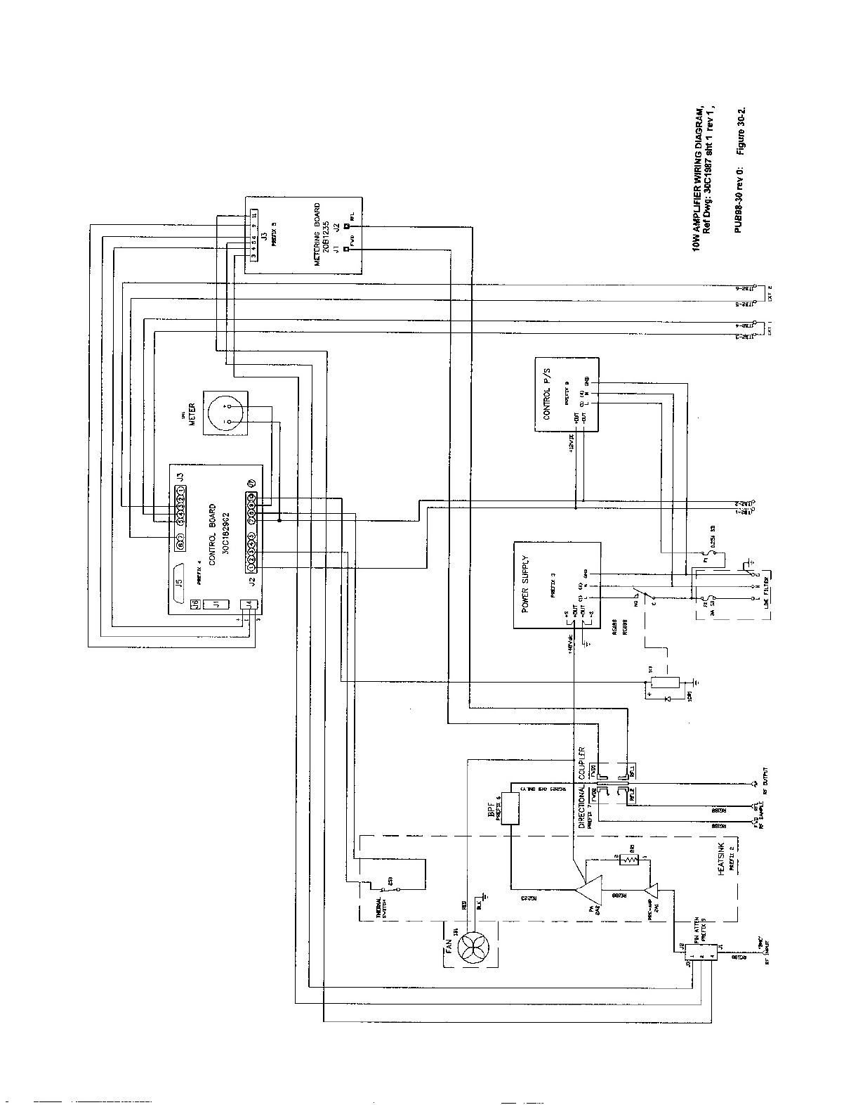
PUB98-30 Amplifier Chassis (Prefix 1):
1. Amplifier Chassis Description ....................30-1
Comment: don't forget to set
the footer date stamp to
release date,and make sure
that any revisions have the
date stamp the same date as
the revision.
MX30V series - 30 Watt VHF AMPLIFIER
PUB98-31 RF Output System: Filter and Directional Coupler (Prefixes 6 & 7):
1. HB Helical Resonator Bandpass Filter Description........31-1
2. HB Low Power Bandpass Filter Description................31-3
3. LB Low Pass & Notch Filter Description..................31-4
4. RF Directional Coupler Description......................31-5
PUB98-32 RF Power Amplifier (Prefix 2):
1. Introduction and General Description....................32-1
2. Preamplifier Circuit Board Assembly.....................32-2
3. RF Power Amplifier......................................32-2
PUB98-33 Amplifier Control Board & Metering Panel (Prefix 4):
1. Control Board & Metering Panel Description..............33-1
2. Amplifier Control Circuit Board Description.............33-2
PUB98-34 Transmitter Output RF Metering Detector Board (Prefix 5):
1. RF Metering & AGC Board Description.....................34-1
2. RF Metering Board Test and Calibration..................34-2
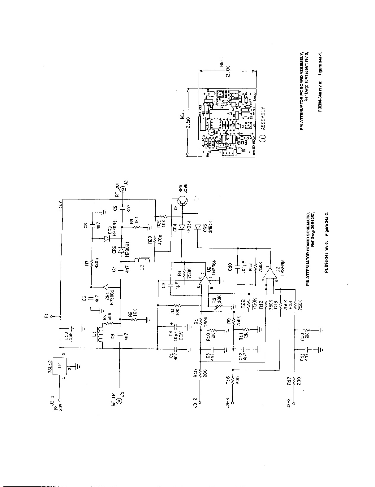
PUB98-34a Pin Attenuator Board (Prefix 9):
1. Pin Attenuator Board Description.......................34a-1
2. Pin Attenuator Board Setup.............................34a-1
INTRODUCTION
This manual describes the LARCAN 30 watt VHF amplifier designed for NTSC
channels 2 through 13. Models 40D2232G1 is for channels 7 through 13, 40D2232G2
for channels 2, 3, and 4, and model 40D2232G3 is for channels 5 and 6. These
amplifiers are used in the LARCAN-USA MX30V series transmitters and translators.
LARCAN all-solid-state 30 W VHF amplifier were designed to operate conservatively
at 30 W peak sync visual RF power and 3 W average aural single carrier RF power,
with superb performance, reliability and operating economy. This amplifier
accepts an on-channel internally diplexed (in a 10:1 ratio vis to aur) composite
driving signal of about 1mW peak visual RF, as input to its RF chain.
The 30 W amplifier and channel processor chassis' are designed to fit in a
single 19" customer-provided cabinet rack, and require 7" (4RU) of vertical panel
space for a complete transmitter or translator system. Alternatively, a 19"
customer-provided tabletop cabinet could be substituted if the site requires it.
The RF amplifier heatsink has its own integral cooling fan, and other sub-
assemblies are convection cooled. The simplicity of design, the deployment of
all modular and other subassemblies, and the use of standard readily available
components, also enhances serviceability.
Peak forward and reflected power are displayed on an analog percent power meter
located on the front panel of the unit.
AMPLIFIER CHAIN
The internally diplexed composite RF output of the channel processor is fed to a
conservatively designed broadband solid-state amplifier. This amplifier requires
no tuning or adjustment. Simplicity of operation, reduced maintenance costs and
increased reliability are a few of the major benefits derived from this
amplifier.
The amplifier chain consists of two stages of amplification for low band and
three stages for high band.
For amplifiers having somewhat more gain than usual, and especially for 10 watt
output applications, the exciter driving the preamplifier may be padded down with
an inline attenuator to avoid overdrive to the preamplifier, because exciters
generally perform better at higher output levels.
The preamplifier uses high gain, broadband, integrated circuit amplifier(s)
operating class A. This preamplifier has two stages in high band models, while a
single stage suffices for low band.
The preamplifier uses the same circuit board that is an integral part of the
"phase quadrature control" that is a required part of paralleled amplifier
configurations. The 30 W transmitter uses a single RF chain, consequently
quadrature phasing is not needed nor used, but some low cost components for it
may remain in place on the board. Removal entails far greater overall expense
than simply leaving them in place.
The PA stage consists of a pair of push-pull FETs in a single case, operating in
class AB as a linear amplifier. This amplifier is capable of more than 50 watts
RF output when driven by the preamplifier in the present system, but uses the
identical dual FET device that is used in higher powered LARCAN transmitters.
The Sound/Aural signal of the transmitter is internally diplexed and corrected at
IF with the visual/vision signal within the exciter, and is amplified in common
with the visual/vision signal in the amplifier chain. Internal diplexing offers
the distinct advantage of lower cost.
The amplifier output is fed through the bandpass filter and the directional
coupler, which provides a small sample of forward and reflected output power for
AGC and VSWR supervisory functions. The transmitter output then passes to the
antenna.
TRANSMITTER CONTROL
The control circuitry in this solid state transmitter is simple. Interlocking in
the 30 W simply consists of jumpers (marked EXT1 and EXT2) but external patch
panel link switches, or RF switching auxiliary contacts, can be connected if
desired. This low power level generally needs no interlocking.
All control wiring of the transmitter passes through a control circuit board
(prefix 4), and facilities are provided on this board for telemetry, status, and
control connections to and from a remote control system.
The transmitter interlock wiring is also brought out on terminal block TB2.
External Interlocks 1 and 2 are all brought out on TB2 for connection as
required. Interlock 1 is provided here only for consistency with other LARCAN
transmitter designs in which this interlock is used with a fire alarm system to
shut off blowers.
In the 10 W, the control is so simple (just a single contactor) that either
Interlock 1 or 2 can be used. The cooling fan for the PA heatsink is wired
across the power supply output, therefore will operate whenever the supply is
energized. A thermostat is provided in the PA heatsink to open the interlock
chain should an unlikely overheating condition occur.
On site it is necessary to ensure that AC mains voltage within ±10% of nominal is
available, especially in sites where the voltage can often be extremely variable,
and/or failures are common. It is a good idea to log all voltage excursions in
such sites over a period of time, and then specify a suitable voltage regulator.
It may be necessary to specify a regulator capable of wide input range if site
voltage variations are extreme.
The amplifier's 48Vdc linear power supply (power-one type HD48-3-A) is rated
for 3A and is designed for operation from AC power line voltage variation of
+10%, -13%. The amplifier takes less than 240 VA.
The control's 12Vdc linear power supply is rated for 0.9A and is powered upon
application of AC into the unit.
ELECTRICAL AND MECHANICAL SPECIFICATIONS
DOC/FCC (NTSC)
Power Output: ................................................................Visual 30 W peak, Aural 3W
Diplexing: ........................................................................internal, 10:1 V to A
Frequency Range: ........................................................54-216 MHz (channels 2 thru 13)
Amplifier Output Impedance: ....................................................................... 50 Ù
Output Connector: ................................................................................type N
Amplifier Input Impedance : ....................................................................... 50 Ù
Output Regulation: .............................................................3% (black-white picture)
Output Variation: .....................................................................2% (over 1 frame)
Amplitude/Frequency Response
-0.75 MHz to +4.75 MHz (Relative to Visual Carrier).........................................+0.5/-1.0 dB
Harmonic Radiation: ..............................................................................-60 dB
Spurious Emission (fv-4.5MHz, fv+9.0 MHz): .......................................................-50 dB
Intermodulation Distortion (3-Tone Method):.......................................................-52 dB
ELECTRICAL AND MECHANICAL SPECIFICATIONS
ELECTRICAL
AC Line Input: ..................................................................................120 VAC
Power Consumption (amplifier alone):
Black Picture and aural on (typical): ....................................................230 VA
ENVIRONMENTAL
Ambient Temperature: ........................................................................ 0° to +45°C
Humidity: .....................................................................................0% to 90%
Altitude: ...................................................................................... 7500 ft.
COOLING
Cooling air enters through the front panel perforations from the room, and passes into the amplifier
heatsink. The rear of this heatsink is fitted with a 4" fan that extracts the warmed air and exhausts it
back into the room. Other parts of the amplifier are convection cooled.
DIMENSIONS
Amplifier and exciter/translator chassis are standard 19" rack width;
Amplifier depth is 19" including a 3" allowance for connectors.
Amplifier height is 5¼" (3U).
The MX30V series amplifier is marketed on the assumption that the customer prefers to provide the cabinet or
enclosure for it.

VHF AMPLIFIER CHASSIS
PUB98-30 rev 0: Dec. 12, 1998 30-1 30W VHF Amplifier
Contents:
Part Topic Page
1 Chassis Description...........................................30-1
List of Figures:
Fig Title Drawing Reference
1 Chassis Assembly Diagram.............................40D2232 sht 1
2 Wiring Diagram, Amplifier, AC Line to Neutral........30C1987 sht 1
3 `power-one' Power Supply Data.....................................
1. Amplifier Chassis Assembly 40D22328G1 through 40D2232G3: Figure 1.
The Amplifier Chassis consists of a standard 19" rack mounted 5¼" 3U enclosure
containing 2 linear power supplies, the amplifier heatsink assembly, the output
directional coupler, the bandpass filter (in most models), a cooling fan, a
control panel (meter and control board), an RF metering board, a line filter, and
an AC relay. Its basic part number is 40D2232.
Three frequency ranges are required to cover the entire VHF television spectrum,
thus there are three fundamental models of RF amplifier assemblies: for channels
2, 3, 4; channels 5, 6; and channels 7 - 13.
AC power input for the three Amplifier/ models is connected for system operation
from one line to neutral, most commonly from 115 volts AC single phase.
40D2232G1 is the chassis for a 30 watt amplifier for operation on channels 7
through 13 (174-216 MHz), it has a 150 watt power supply, and its AC
is connected line to neutral.
40D2232G2 is the chassis for a 30 watt Amplifier for operation on channels 2,
3, and 4 (54-72 MHz), it has a 150 watt power supply, and its AC is
connected line to neutral.
40D2232G3 is the chassis for a 30 watt Amplifier for operation on channels 5
and 6 (76-88 MHz), it has a 150 watt power supply, and its AC is
connected line to neutral.
Although we indicate NTSC frequency ranges, the amplifiers are capable of
frequency coverage outside the ranges cited, for CCIR systems B, D, etc.
transmitter applications in other regions worldwide.
Figure 1 is the fundamental assembly drawing of the chassis.
The heatsink cooling fan is a 48 volt DC "Muffin" model from Comair-Rotron; it is
Comment: The footer date stamp
must be altered to agree with
the revision date.
VHF AMPLIFIER CHASSIS
PUB98-30 rev 0: Dec. 12, 1998 30-2 30W VHF Amplifier
powered from the 48 volt amplifier power supply. As built, the cooling fan pulls
warmed air from the heatsink so the cooling air enters through the perforations
in the chassis front panel. This may be more convenient for a desktop cabinet
arrangement, but for cabinet racks fitted with ventilation filtering, the fan can
be mechanically reversed end for end, and remounted so that the fan forces air
through the heatsink, from which the warmed air exhaust leaves the chassis
through the front panel perforations.
A thermostat is mounted on the heatsink where operating temperature can be
sampled. If this temperature should increase past the trip point of the
thermostat,which is 60°C, its contacts will open and break the interlocking
circuit of the amplifier. The interlock circuit ultimately controls the power
supply to the amplifier, and the power supply will therefore shut down and remain
shut down until the heatsink cools and the contacts close again.
The chassis is wired according to one of the wiring diagram shown on Figures 2.
Chassis parts lists are provided on the last pages of this manual. The circled
numbers on the assembly drawing correspond to the "symbol" item numbers on the
parts list.
40D2168Gx means that the assembly can be any one of the 3 listed above, where "x"
denotes the group.

Contents:
Sec Topic Page
1 HB Helical Resonator Bandpass Filter Description (50W HB only)31-1
2 HB Low Power Bandpass Filter Description......................31-3
3 LB Low Pass & Notch Filter Description........................31-4
4 RF Directional Coupler Description............................31-5
List of Figures:
Fig Title Drawing Reference
1 Bandpass Filter response...........................text, page 31-2
2 Bandpass Filter schematic..........................text, page 31-3
3 RF Directional Coupler schematic....................text, page 8-6
4 Generic Helical Resonator Bandpass Filter Assembly...30C1064 sht 2
5 High Band Bandpass Filter Assembly....................20B704 sht 1
High Band Bandpass Filter Schematic...................10A769 sht 1
6 Low Band Bandpass & Notch Filter Assembly............20B1118 sht 1
Low Band Bandpass & Notch Filter Component locations.20B1120 sht 1
7 Low Band Bandpass & Notch Filter Schematic...........20B1151 sht 1
8 RF Directional Coupler Assembly.......................20B534 sht 4
Low Band Coupler PC Board Assembly...................10A1942 sht 1
1. 30C1064G1 Helical Resonator Bandpass Filter (used with 50 watt High
Band):
The helical resonator was developed during the late 1950's and first described in
"Proceedings of the IRE" magazine by W. W. McAlpine and R. O. Schildknecht,
"Coaxial Resonators with Helical Inner Conductor," Proceedings of the IRE, vol.
47, no. 12, pp. 2099-2105; December, 1959. The same authors later published
another magazine article "Helical Resonator Design Chart," Electronics, p. 140;
12 August 1960.
IRE stood for the "Institute of Radio Engineers" which was responsible for some
of the television transmission standards that remain in use today. IRE later
merged with the "American Institute of Electrical Engineers" to become the
"Institute of Electrical and Electronic Engineers" which is known to us as the
"I-triple-E" and which continues publication of important electrical and
electronic engineering research papers in the "Proceedings of the IEEE" and in
the "IEEE Transactions" dealing with electrical and electronics interests.
We generally avoid such papers in our manuals except for the rare instance where
critical information is involved, as the content of most of these publications
are considered to be excessively arcane and esoteric for the beleaguered
technician whose sole interest is to get the transmitter back on the air. Should
you wish further information, we refer you to the above cited publications, to
"Reference Data for Radio Engineers, sixth edition" published by Howard W. Sams &
Co., and to the "ARRL Radio Amateur's Handbook" published annually by the
Comment: T
he footer date stamp
is frozen. Any later
revisions made after the
initial release must have the
footer date agree with the
revision date.
1. Bandpass Filter: (continued).
LARCAN bandpass filter implementations generally consist of a cascaded series of
coupled resonators. Some use helical resonators; essentially a self supporting
high Q coil (the helix) mounted inside a metallic shield enclosure. One end of
the coil is solidly connected to the shield enclosure and the other end is open
circuited except for a small trimmer capacitance to ground. The dimensions of
the coil are critical to the frequency of operation; the assembly behaves as
though it were a quarter wave coaxial transmission line resonator. Several sizes
of coils and enclosures are necessary to cover the desired frequency ranges.
Fold-out Figure 4 indicates the generic assembly of a coupled helical resonator
bandpass filter.
The referenced drawing in Figure 4 happens to be a low band filter, but the high
band unit is laid out identically and appears almost the same as Figure 4 except
the high band helixes have fewer turns of coarser winding pitch, and their shield
enclosure dimensions are somewhat smaller.
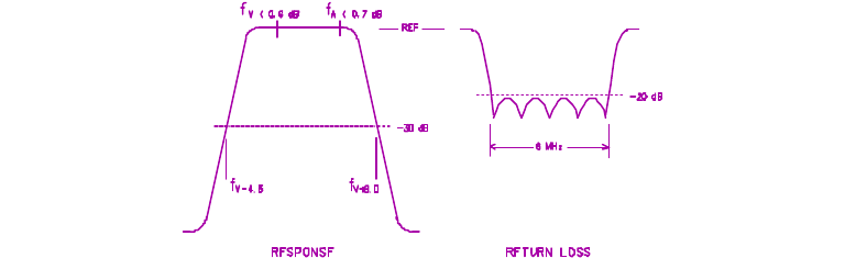
The desired response shape is presented as Figure 1 below, and the filter
electrical equivalents are presented on the next page as Figure 2. When we
examine the assembly, and take capacitances into account, the equivalent circuit
of a helical resonator becomes simply a parallel resonant LC tank circuit having
low (trimmer) capacitance and relatively high inductance. Adjustment of the
trimmer produces a change of capacitance, and the trimmer's moveable slug is
shaped to appear as a shorted turn, which alters the inductance of the helix.
Matching from and to 50 ohm transmission lines is accomplished with taps on the
input and output helixes.
Coupling between sections is electrically a bridged T network of capacitors, and
is made up of the small capacitance between the free ends of the coils,
controllable by the amount of capacitance to ground that is introduced by the
coupling adjustment screws; the coupling is maximum when the screws are backed
out fully from the enclosure. Shielding partitions placed inside the enclosure
between helixes, produce fixed area apertures which affect the coupling
capacitance between helixes. Helix #3 in the Figure 4 drawing has taller
partitions on both sides of it, giving lower capacitance and less coupling than
the others.
For system use, the tuning and coupling is adjusted for a flat topped response
with steep sides, and the desired shape is such that f
V - 4.5 MHz and
fV + 9.0 MHz are both 30 dB down, but the carriers must be f
V < 0.6 dB and
fA < 0.7 dB departure from flatness. Input and output return loss must be 20 dB
or better over the full 6 MHz bandwidth. These idyllic sweep curves are shown
below as Figure 1.
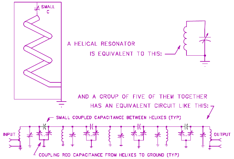
This is the electrical equivalent of a series of five coupled helical resonators.
Similar lower power filters are built using conventional air wound coils and
ceramic trimmer capacitors, and these will be described next:
2. 20B704G1 Low Power Bandpass Filter for High Band:
Please refer to Figure 5. The configuration of this filter is similar to the
previously described helical resonator type in that it uses five LC resonant
circuits, but it differs in that two of these resonant circuits behave as high Q
traps for frequencies outside the band edge (_4.5 and +9 MHz), so that the
overall response has a reasonably flat top and steep sides. Factory adjustment
is made to achieve the same in-band response (carriers must be fV < 0.6 dB and
fA < 0.7 dB departure from flatness) as described for the helical resonator
filter. (We would have preferred to use this 20B704G1 filter for the 50 watt
high band system as well, except that the ceramic trimmers overheated due to the
higher RF currents at the 50 watt level, so the decision was made to go with the
higher power helical resonator filter for 50 watt high band transmitters).
Like the helical resonator filter, there are nine screw adjustments and two I/O
matching (with soldering iron) adjustments that need to be made simultaneously,
and all of them are interactive. Accurate adjustment is impossible without the
aid of a network analyzer, and because of the expense of this gear it is not as
likely to be available in the field; for this reason we say the filter is not
user-adjustable.
Sure, it is possible to use a sweep generator and detector for setting the
response of either filter, but unless an accurate 50 ohm return loss bridge is
used with the sweep generator, there is no way to properly set up the input and
output matching. Our recommendation: don't mess with the filter adjustments at
all.
3. 20B1118G1 Low Pass and Notch Filter for Low Band:
Please refer to Figures 6 and 7. Ten adjustable inductors, four fixed inductors
(which also can be adjusted slightly by spreading their turns with a suitable
tool), and twenty-one fixed capacitors, make up the complete filter.
Functionally, it consists of two sections of shunt m-derived low pass network,
followed by four bridged-tee notch networks. Its signal direction is intended to
be one way only, as indicated in Figure 7.
The low pass section (L1, L2, C1 thru C5) of the filter is designed to cut off at
a frequency lower than the second harmonic, so that only the fundamental is able
to pass through, but harmonics are blocked.
The four notch sections are tuned to reject fV_9, fV_4.5, fV+9, and fV+13.5 MHz
(down typically 18, 30, 24, and 26 dB respectively - sometimes one of the tuned
circuits at fV_9, either L3 or L5, is readjusted to fV_4.5 in order to make that
notch deep enough that the fV_3.58 MHz component is sufficiently attenuated).
L4, L7, L10, and L13 are adjusted to set the width and depth of the notch. A
typical network analyzer transfer function plot of the filter indicates the four
notches at the values stated above, and the band pass of the f
V and f
A
frequencies and the channel between, having less than 0.1 dB of ripple.
If your particular filter appears to be missing some of its capacitors, don't be
concerned. Probably the "missing" ones are chip capacitors soldered to the pads
on the underside of the board. The circuit board is a mature design which was
made before surface mount components were in widespread use; occasionally we run
out of low value capacitors having leads. Most RF parts used these days are
surface mount.
4. RF Directional Coupler:
A directional coupler is based on the principles of inductive (magnetic) coupling
and capacitive coupling.
In the LARCAN quad directional coupler implementation as shown in Figure 3
(schematic equivalent) and Figure 8 (assembly), the RF to be sampled passes
through a microstrip transmission line that is connected between the transmitter
output filter at J3 and the antenna system at J4. The magnetic field surrounding
the hot conductor of this transmission line induces a small RF current flow in
other conductors situated parallel to it. One end of each sampling conductor is
terminated by a resistor to ground. Sometimes small capacitors are connected
across these resistors to provide a termination that remains resistive over the
band. The other end of each sampling conductor connects to an external load,
usually a 50 Ù input of something such as an RF detector for AGC, the station
demodulator, or an RF detector for VSWR sensing.
If the sampling system as described in the forgoing paragraph were dependent only
on magnetic coupling and absolutely no capacitance were present, the external
loads would be driven with RF samples regardless of the direction they came from.
Omnidirectionality is not wanted; our objective is that the system should be
directional, that is, a signal coming from the transmitter should be seen by the
"forward" ports, and a signal reflected back from the antenna should be seen by
the "reflected" ports, but at the same time as little as possible of the forward
signal from the transmitter should be seen on these reflected ports.
The desired directivity is achieved by the capacitance between the main line and
each sampling line. The presence of this capacitance changes the relative phase
of the RF signal seen in the sampling line such that the capacitively coupled
signal adds to the inductively coupled signal at the end of the line nearest the
signal source, and subtracts from it at the other end, thus the sample becomes
directive.
This capacitance is trimmed by small "gimmick" capacitors designated (believe it
or not) L1 thru L4. This designation arose from a mistaken belief that
"inductances are made of wire; ergo, these are inductances." They are in reality
short pieces of Teflon sleeved magnet wire which, although they may possess a
fraction of a nanohenry of inductance, are mainly small capacitors which are
factory adjusted by bending the wire to control the amount of coupling
capacitance between the transmission line and the sampling loop concerned. The
position of the capacitor along the loop does not seem to matter.
Terminations are provided at the subtractive ends of each of the four sampling
lines.
In the enclosure shown in Figure 4, J3 and J4 are the filter and antenna ports
respectively, and J1, J5 are "forward" samples which are maximum amplitude for
signals incident on J3; while J2, J6 are "reflected" samples which are maximum
amplitude for signals incident on J4.
Different coupling values are obtained from the spacing of conductors; the nearer
the spacing, the greater the coupling. Coupling is also greater according to
frequency, and rises at a rate of about 6 dB per octave. In the boards shown in
Figure 4, the J1 and J2 signals will be about 10 dB greater amplitude (about
36 dB below the generator level at 70 MHz on low band or 200 MHz on high band)
than the signals sampled from J5 and J6 (about -46 dB). Generally for system
purposes the reflected signal sample to the VSWR supervisory system should be
taken from the J2 connector because it has greater coupling and we need to
measure a much smaller signal in a detector having finite small-signal
sensitivity. System forward signals can be taken from J1 for the AGC detector,
and J5 for the system monitoring demodulator.
A network analyzer and extremely accurate terminations are required for setting
up the directional coupler. The adjustments are made to the trimming
capacitances "L1" thru "L4", and the capacitors in parallel with resistors R1
through R4. Our target is directivity of 30 dB or better on each sampling port,
and coupling (forward direction) for J1 and J2 about 36 dB down, J5 and J6 about
46 dB down.
No user adjustments are possible nor recommended. Very little can go wrong with
the directional coupler other than from the antenna being hit by lightning, and
inspection is all that is recommended, nothing more.

Contents:
Sec Topic Page
1 Introduction and General Description..........................32-1
2 Preamplifier Circuit Board Assembly...........................32-2
3 RF Power Amplifier............................................32-2
List of Figures:
Fig Title Drawing Reference
1 PA & Preamplifier Assembly.....................30C1899 sht 1 rev 1
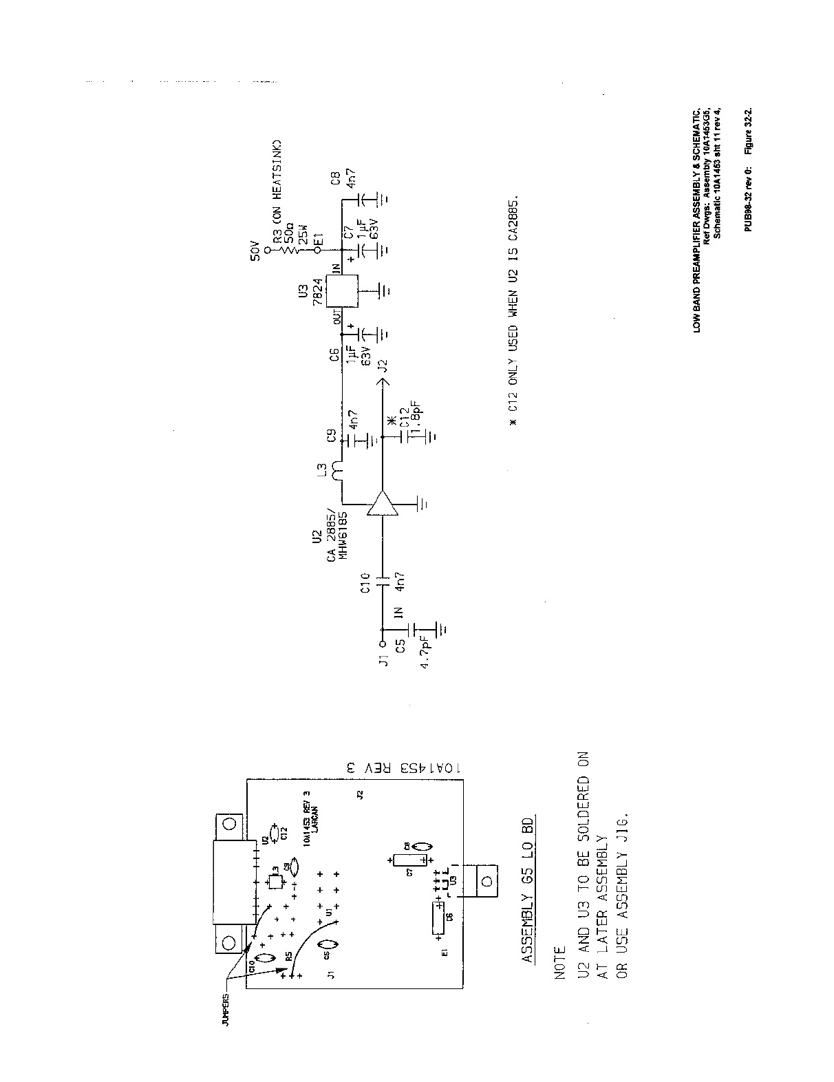
2 Preamplifier Board Assembly, Low Band..........10A1453 sht 9 rev 3
Preamplifier Schematic, Low Band..............10A1453 sht 11 rev 4
3 PA Input Board Assembly, Low Band..............30C1054 sht 1 rev 5
4 PA Output Board Assembly, Low Band.............30C1055 sht 1 rev 3
5 PA Schematic, Low Band.........................30C1056 sht 1 rev 2
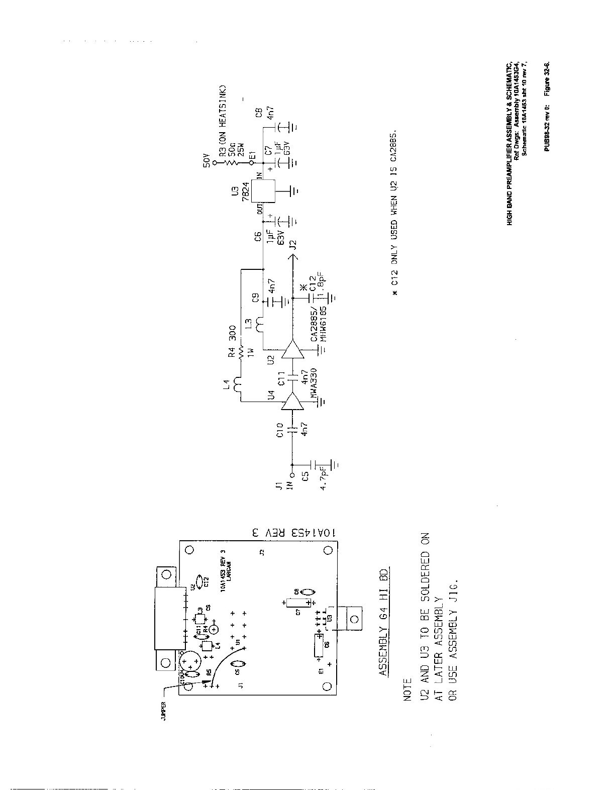
6 Preamplifier Board Assembly, High Band.........10A1453 sht 9 rev 3
Preamplifier Schematic, High Band.............10A1453 sht 10 rev 7
7 PA Input Board Assembly, High Band.............20B1222 sht 1 rev 8
8 PA Output Board Assembly, High Band............20B1226 sht 1 rev 7
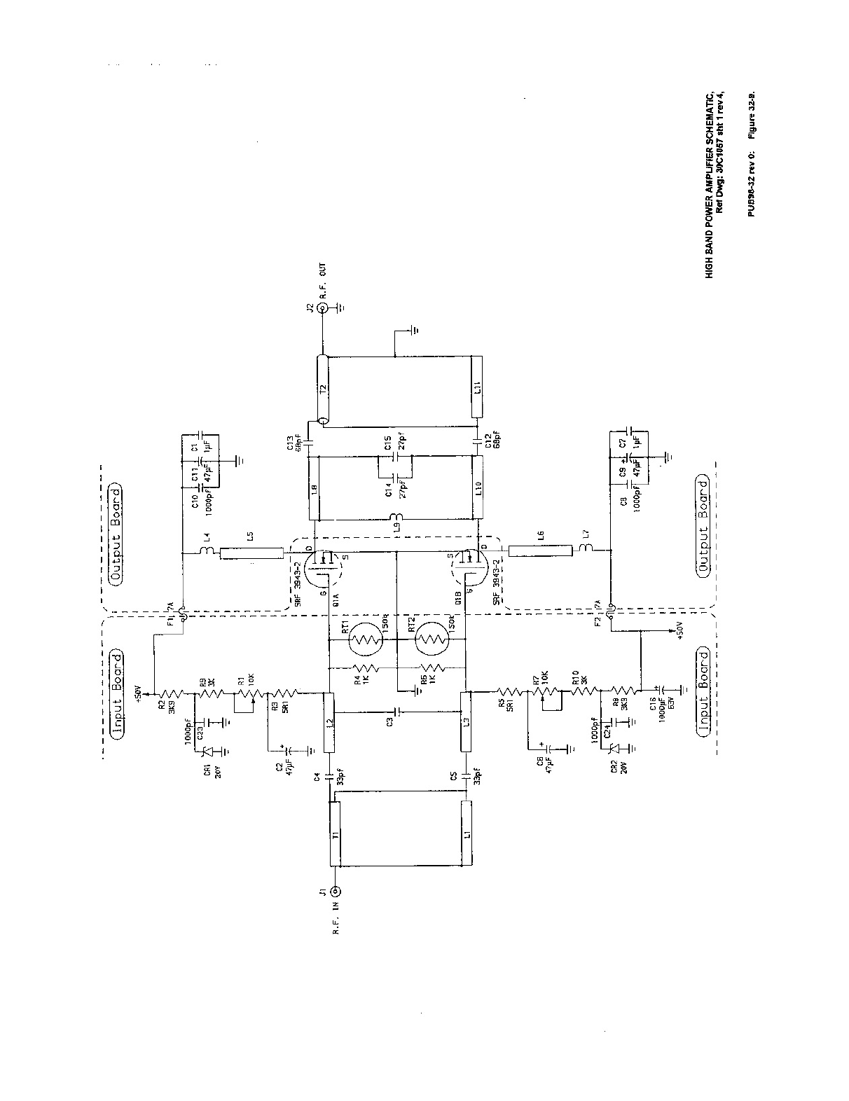
9 PA Schematic, High Band........................30C1057 sht 1 rev 4
1. RF Power Amplifier & Heatsink Assembly 30C1899G1 - G2 - G3: Figure
1.
The 30C1899 RF Power Amplifier basically consists of a fan-cooled heatsink and
three circuit boards. These boards are the Preamplifier board, the Amplifier
Input board, and the Amplifier Output board. This subassembly is mounted in the
Transmitter Chassis (as an example, see drawing 40D2008 - Figure 1 of the 10W/50W
Chassis section). Figure 1 shows the basic construction of the RF PA assembly.
A directional coupler (example shown as item 15 on the 10W/50W Chassis Assembly
diagram Figure 07-1, and described in the RF Output section of this manual) is
also mounted in the chassis and provides an AGC and metering DC signal
corresponding to the amplifier output RF.
Figure 32-1 illustrates the arrangement of boards on the amplifier heatsink.
Cooling for the PA heatsink is provided by a 4" axial flow Rotron fan which is
mounted on a bracket situated at the end of the heatsink, so that the fan can
extract air through the finned portion of the heatsink. Air exhaust is normally
to the rear of the chassis. If this is not suitable for the application, then
the fan can be mechanically reversed so that it blows air into the heatsink
instead, and this air would then exhaust through the perforations in the front
Comment: The footer date stamp
must agree with the revision
date. Fix it if it doesn't.
Rev date and footer date must
be the same.
panel.
The heatsink fan can move approximately 100 cfm of cooling air, and has a DC
motor that is powered by the same +50 volts that operates the amplifier.
1.RF Power Amplifier & Heatsink Assembly 30C1899G1 - G2 - G3:
Most LARCAN exciters produce their best linearity at or near their maximum rated
output levels, and often the overall system gain is sufficient to result in
overdrive of later stages of the transmitter. The transmitter or translator
lineup may therefore include an in-line attenuator between the exciter and the
preamplifier, to prevent overdrive from certain models of exciter-modulator.
This is especially true for the 10 watt system, because in our basic transmitter
family a 10 watt amplifier is simply a lightly driven 50 watt amplifier, and a 50
watt amplifier is likewise a lightly driven 250 watt output stage running without
its driver/IPA. (Our 250 watt transmitter lineup needs an additional IPA to get
enough drive to the identical final stage that is used in the 50 watt and 10 watt
lineups).
2.RF Preamplifier 10A1453G5 (Low Band) and 10A1453G4 (High Band):Figures 2 and 6.
This preamplifier design originally appeared in the aural/sound section of a dual
RF chain transmitter which operates two single RF chains in quadrature and
therefore requires phase and gain control of the input to each chain. The same
unpopulated circuit board is used for the present application, therefore has the
pads and holes for the components which performed the adjustment of RF gain and
phase in the parallel systems. In a single chain transmitter such as the present
one under discussion, there is no requirement for control of RF phase nor
consequently its components; they are therefore removed and wire jumpers
substituted.
In the Low Band preamp, the 50 Ù input cable is matched by C5, which uses the
inductance of the traces on the PC board to form a low pass matching network, and
fed to amplifier U2 whose output connects through a cable to the PA. U2 is a
linear amplifier designed originally for use as a wideband cable system trunk
amplifier. Cable amplifiers are nominally 75 ohms in and out, but the MHW6185 is
capable of a good match with 50 ohm source and load. C12 and the lead inductance
of a CA2885 when used as U2, perform output matching to 50 Ù. C12 is not
present in a board using an MHW6185 for U2. The gain of U2 is spec'd as 18 dB,
and allowing a few dB of losses, the gain of the Low Band preamp is 14 to 16 dB.
RF power FETs operated in High Band amplifiers exhibit about 6 dB less gain than
they do in Low Band, so an additional amplifier is necessary to make up the
difference. The High Band preamplifier therefore consists of two stages.
In the High Band preamp, the input is matched by C5 and the PC trace inductance
which together forms a low pass matching network, and the signal is fed to an
additional preamplifier stage U4, whose output appears as the input of U2, which
in turn feeds the board output cable. The specified gain of type MWA330 in the
U4 position is 6 dB, and a type MHW6185 or CA2885 (U2) is 18 dB. A few dB of
losses exist on the board, so the effective gain of the High Band preamp board
10A1453G4 is about 20 to 22 dB.
High Band preamps 10A1453G1 used in higher powered externally diplexed
transmitter aural service, have a type MWA130 instead of an MWA330 for U4.
Specified gain of an MWA130 is about 12 dB, but we don't recommend substitution
of U4 in any internally diplexed system due to overall linearity and intermod
requirements which are much more stringent in the internally diplexed case. This
is because the 30 dB (or thereabouts) of aural to colour subcarrier isolation
normally provided by the diplexer is not there, and it simply means that
internally diplexed system intermod numbers have to be much better.
At the output of U2, a match to 50 Ù is provided by C12 and the device lead
inductance, which together create a low pass matching network in boards where a
type CA2885 cable amplifier is used; conversely a type MHW6185 device
characteristics give it a wideband match to 50 Ù therefore no special output
matching is necessary, and C12 is not present.
U3 is a voltage regulator providing +24 V to the preamplifier stage(s).
3. SRF 3943-2 RF Power Amplifier: Figures 3, 4, 5, 7, 8, and 9.
The Power Amplifier (PA) is configured in push-pull, using dual N-channel
enhancement mode Field Effect RF power transistors which are packaged into a
single case and operated in class AB.
The Low Band and High Band versions of the PA differ slightly due to the
frequency ranges to be covered.
3.1 Low Band PA Circuit Description (30C1054 input board, 30C1055 output board)
The PA consists of two, source grounded N-channel, insulated gate Field Effect
Transistors (FETs) packaged in a single case, operating class AB in a push-pull
configuration. The original schematic indicates a type MRF-151-G as the dual FET
used; we now use a "selected MRF-151-G to tightly controlled specifications"
which is proprietary to LARCAN and designated type SRF 3943-2. This selection
simply tightens the gain specification for operation in High Band, and in case of
emergency, there is no reason an MRF-151-G could not be substituted for Low Band
operation.
Because these FETs are "enhancement mode N-channel" devices, they require
positive gate-to-source bias voltage on each gate to cause source-drain
conduction. The quiescent Class AB idling bias current is set at 0.6 ampere for
each half. The gate voltage required to produce this idling current may vary
between 2 V and 5 V according to the device specification sheet, and typically is
3 to 4 V. FET gate threshold voltages also are temperature sensitive, so thermal
compensation is provided by RT1 and RT2.
Gate bias is supplied out of adjustable voltage dividers from +20 V regulated
bias sources CR1 and CR2. Current limiting to these zener diodes is provided
through R1 and R8. Resistors R9, R2, R3, R4, and RT1 provide gate bias for the
"A" half of the amplifier; R10, R7, R6, R5, and RT2 provide bias for the "B"
half.
The RF input signal arriving in J1 is applied to balun T1 to provide two signals
180° out-of-phase. These antiphase signals are stepped down to match the low
input impedance of the FET through a ð-network consisting of C1, C2, C3, L1, L2,
C4, and the device input capacitance, and then applied to the gates. The
capacitance value of C4 is changed for operation on channels 5 & 6. The gate
input impedance at the operating frequency is low compared with the values of R3
and R6, which have little or no effect at RF.
R3 and R6 provide a DC path for bias, and provide loading at lower frequencies
where gate impedance is high, in order to assist in maintaining amplifier
stability. The choice of C6, C7, C20, and C21 values, their series inductances,
and that of board traces, also ensures effective bypassing at critical
frequencies.
The output matching ð-network, consisting of inductors L3 thru L8, and
capacitances C13 thru C16, transforms the very low output impedance of the FET,
upwards to a standard 50 Ù. The two antiphase output signals are finally
combined in balun T2, L9. Jumpers placed across parts of L7 and L8, plus the
changed values of C13, C14, C15 and C16, configures the system for channels 5 & 6
operation.
DC is applied to the FET drains through L3, L4 for the Q1A half, and L5, L6 for
the Q1B half. L3 and L6 are short sections of microstrip line which transform
the apparent RF impedances of L4 and L5 to higher values as seen by the FET. RF
and lower frequencies are bypassed with paralleled C9, C10, and C17 for the "A"
half of the amplifier, and C11, C12, and C18 for the "B" half. These groups of
capacitors are selected in value and for their internal equivalent series
inductances so that they will be an effective bypass at critical frequencies of
interest, including video, to assist in maintaining stability. The connections
for C20 and C21 also assist in stability due to their return paths through the
ground plane of the output board. This connection provides a small amount of
negative feedback as a primitive means of neutralizing the amplifier.
The RF output leaves the board from J2.
3.2 Low Band PA Setup Procedures
1. Set up a 48 V power supply, current limited to a little more than 1.2
amps.
2. Remove both fuses on the power amplifier. Turn both bias potentiometers to
their maximum resistance position ( minimum gate voltage).
3. Apply the 48V supply to the B+ terminal. Verify that the bias (gate)
voltage is at or near minimum by measuring the dc voltage at the gates of
the device. This voltage should be less than 1V. Install one of the fuses
and slowly adjust the corresponding bias potentiometer for 500 mA drain
current. Transfer the fuse to the other side and adjust the corresponding
pot for 500 mA of drain current.
4. Connect a 20 dB, 1 W attenuator to the output of the amplifier as shown in
the diagram below.
5. Install bothl fuses and apply B+ to both supply connections of the
amplifier module.
6. Apply a low level sweep to the amplifier and measure the DC input current
(not more than 1.2 amps) and gain. Gain of the amplifier alone should be
about 20 to 23 dB, and with the preamp in circuit the combined gain should
be between 40 and 43 dB. Flatness over the band should be better than
1 dB, as shown in the following diagram. Curves for chs 2-4 and 5,6 are
correct for the PA alone:
3.3 High Band PA Circuit Description (20B1222G2 input board, 20B1226G1 output
board)
The PA consists of two, source grounded N-channel, insulated gate Field Effect
Transistors (FETs) packaged in a single case, and operating in a push-pull
configuration in class AB. A single specially characterized device designated
SRF 3943-2 is used for this High Band amplifier. These N-channel FETs are
"enhancement mode" devices, so require a positive gate-to-source bias voltage on
each gate to cause source-drain conduction. Quiescent Class AB idling bias
current is set at 0.6 ampere for each half.
The gate voltage required to produce this idling current may vary between 2 and 5
V due to variances among FETs, and typically is 3 to 4 V. Gate voltages also are
temperature sensitive, so temperature compensation is provided by RT1 and RT2.
Gate bias is supplied out of adjustable voltage dividers from +20 V regulated
bias sources CR1 and CR2. Current limiting to these zener diodes is provided
through R2 and R8. Resistors R9, R1, R3, R4, and RT1 provide gate bias for the
"A" half of the amplifier; R10, R7, R5, R6, and RT2 provide bias for the "B"
half.
The input RF arriving in J1 is applied to balun T1, L1 to provide two signal
outputs 180° out of phase. These signals are stepped down to match the low input
impedance of the device through a dual section, twin ð network consisting of C1,
C2, L2, L3, C3, and the device input capacitance, and then applied to the gates.
The gate impedance at the operating frequency is much lower than R3 and R5, so
these resistors have little or no effect at RF.
R3 and R5 provide a DC path for bias, and provide loading at lower frequencies in
order to assist in maintaining amplifier stability. The choice of C2 and C6
values, and their internal equivalent series inductances, also ensures effective
bypassing at critical frequencies.
The output matching ð network, consisting of inductors L5 thru L10, and
capacitances C12 thru C16, tunes out the FET drain capacitance and transforms the
very low output impedance of the FET, upwards to a standard 50 ohms. The two
180° antiphase output signals are finally combined in balun T2, L11.
DC is applied to the drains through L4, L5 for the "A" half, and L6, L7 for the
"B" half. L5 and L6 are also short sections of microstrip transmission line
which transform the apparent RF impedances of L4 and L7 to higher values seen by
the FET. RF and lower frequencies are bypassed with C1, C10, C11, and C8, C9,
C7.
These groups of capacitors are selected in value and for their internal
equivalent series inductances so that they will be an effective bypass at all
frequencies of interest including video, to assist in maintaining stability.
Towards this objective of stability, in addition to resonating with the device
drain-to-drain capacitance at RF, inductor L9 places a heavy load on the FET
output at low frequencies, where it behaves as a dead short.
3.4 High Band PA Set Up Procedures
1. Set up a 48V power supply, current limited to a little more than 1.2 A.
2. Remove both fuses on the amplifier. Turn both bias potentiometers to their
maximum resistance (minimum gate voltage).
3. Apply the 48V supply to the B+ terminal. Verify that the bias (gate)
voltage is at or near minimum by measuring the voltage at the gates of
the device. This voltage should be less than 1V. Install one of the fuses
adjust one of the potentiometer for 500 mA drain current. Then adjust the
other potentiometer for a total current of 1A.
4. Connect a 20 dB 1W attenuator to the output of the amplifier as shown
below.
5. Apply B+ to both supply connections of the amplifier.
6. Apply a low level sweep to the module and measure the DC input current
(about 1.2 amps) and gain. Amplifier gain by itself should be 15 to 17
dB, and with preamp included, overall gain should be between 38 and 41 dB.
Sweep response should be flat within 1 dB over the band as shown in the
sweep diagram from page 4, repeated below. Note that these sweep curves
are applicable to the push-pull FET amplifier only and the preamp is not
included.

Contents:
Sec Topic Page
1 Control & Metering Panel Description..........................33-1
2 Amplifier Control Circuit Board Description...................33-2
List of Figures:
Fig Title Drawing Reference
1 Amplifier Control Board Assembly.....................30C1829 sht 8
2 Amplifier Control Board Schematic..........................20B2438
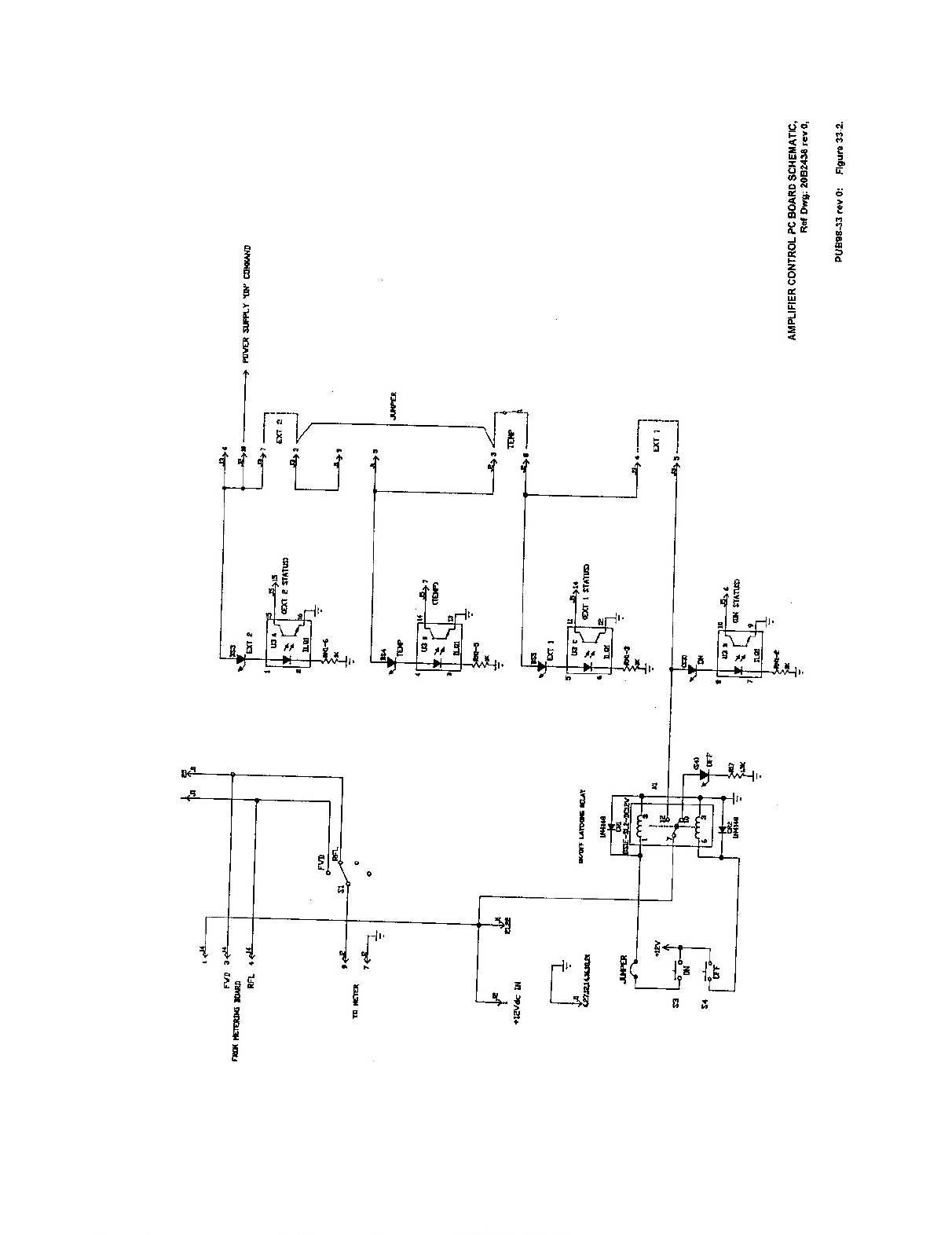
1. Control Panel:
Amplifier control and monitoring is performed by the Control and Metering Panel.
This 19" wide, 3 unit (5¼") panel serves primarily as a mechanical mounting for
the amplifier's control switches, status indicator lights, and a multifunction
meter. The panel is the mounting for the control circuit board described below,
and elsewhere on the chassis is an output metering circuit board which is
described later in this manual.
The Amplifier control panel features as seen from the front, are these:
1. 50 ìA panel meter fitted with a power scale calibrated 0-125 percent;
2. The meter input selector switch for forward and reflected power;
3. Pushbuttons for ON & OFF;
4. Three LEDs providing indications (from left to right) when lighted: EXT 1
interlock is closed,the output amplifier TEMP thermostat is cool, EXT 2
interlock is closed.
The amplifier is provided with a VSWR cutback function that reduces its power
output to save it from harm in the event of very high reflected power such as an
open circuit condition.
The VSWR cutback feature is described in the Metering board section of this
manual.
Comment: The footer date stamp
must agree with the revision
date.
2. Amplifier Control Circuit board Assembly 30C1829G2: Figures 1 and 2.
There are seven connectors on the Control circuit board. These connectors
perform the following functions:
J2 connects elsewhere in the amplifier, such as the thermal switch, relay, and to
the 50 ìA meter.
J3 connects to the external interlocks.
J4 interconnects with J3 of the Metering board.
The transmitter interlock chain begins with the +12V at K1-7. When K1 is set ON
by energizing its coil K1-1, contacts 7 and 12 close and contacts 7 and 10 open,
turning off the LED inside the OFF button S4. The +12V from closed contact 7-12
lights the LED inside the ON button S3 and lights the optodiode in U3D, which
provides a logical active low out of its pin 10 for a remote control status
interface. This status signal simply tells the remote control through J5-6 that
the transmitter was instructed to be ON, nothing more.
The +12V from contact 7-12 also comes out of the board on J3-5, which is one side
of the EXT 1 interlock. EXT 1 in larger transmitters is often used with a fire
alarm system to stop all blowers, and in lower power transmitters it is still
worthwhile that a normally closed fire alarm contact be connected to EXT 1
because the fan(s) in the transmitter could cause enough air currents in the
transmitter room to fan the flames.
When the EXT 1 interlock is closed and the +12V appears on J3-4, the +12V is now
at DS5 (marked EXT 1) and the optodiode of U3C which both light up to say EXT 1
is closed. The active low from U3C pin 11 informs the remote control via J5-14
that EXT 1 interlock is closed.
The +12V now is applied to J2-8 which connects to a normally closed contact in a
thermostat that responds to the temperature of the RF power amplifier. If a
cooling fan should stop and the amplifier should overheat, this contact will open
and prevent the +12V from appearing at J2-3. This of course breaks the chain and
removes the 12V from the solenoid of the power supply contactor.
Assuming the thermostat is cool, DS4 and the optodiode in U3B are lighted,
confirming TEMP is okay. The logical active low out of U3B pin 14 informs the
remote control of this fact through J5-7.
Assuming the thermostat is closed, the +12V next appears at J3-3, which is EXT 2
interlock. This is the place where RF patch panel link contacts or coaxial
switch auxiliary contacts, and/or dummy load thermostat contacts would be
connected so that the transmitter can only be ON when valid RF paths are present,
2. Amplifier Control Circuit board Assembly 30C1829G2: Figs 1 and 2.
Finally, when the interlock chain is complete, the +12V is applied to the
solenoid of the power supply primary contactor through J2-10, and the cooling
fans and power supply are all turned on. The DS3 LED marked EXT 2 is lighted, as
is the optodiode in U3A. The output active low from U3A at pin 15 informs the
remote control via J5-15 that the EXT 2 interlock is intact.
The interlocked +12V is also available at J3-6 so it can be used for special
on-site control functions.
The amplifier AGC system (overdrive protection) is based on an RF attenuator
located at the input stage of the amplifier, and this is controlled by DC voltage
supplied from RF detectors which sample the RF output from the amplifier. If the
output rises, the DC voltage increases, and this increases the amount of
attenuation, thus the output is maintained at a constant level. The majority of
the AGC processing is done by analog op-amp circuits in the Metering Board, but
the initial threshold setting is done in the pin attenuator board, potentiometer
R5. These simply provide an adjustable reference bias voltage to the AGC
circuit, which adjusts the power output inversely according to this bias voltage.
In the event of a VSWR that exceeds a preset amount, the AGC voltage becomes
modified a little to reduce the amplifier output by an amount proportional to the
reflected signal. This "VSWR Cutback" permits the amplifier to remain on the air
at reduced power if the antenna should gradually accumulate a layer of ice.
The AGC voltage and modifications to it from VSWR, are summed in U2A which is
basically a buffer amplifier that also provides a telemetry output to the remote
control system through J5-3.
Forward and Reflected meter calibration is done with potentiometers on the
Metering Board.
A 50 ìA meter mechanism that is fitted with a scale 0-125%, is connected to J2-9
and J2-7. The + terminal of the meter connects to J2-9.
Although F1 is drawn in Figure 2 as a fuse, in reality it looks like any ordinary
disc ceramic capacitor, but it is a current limiting device similar to a
thermistor having an extreme positive temperature coefficient. In normal
operation it maintains a low resistance, until it gets hot from too much current
and then suddenly switches to a high resistance state so that the current it is
able to pass is only a very small amount. This small amount of current is
sufficient to keep it warm enough that it remains in its high resistance state.

Contents:
Sec Topic Page
1 RF Metering Board Description.................................34-1
2 RF Metering Board Test and Calibration........................34-3
List of Figures:
Fig Title Drawing Reference
1 Metering Board Assembly..................................20B1235G7
2 Metering Board Schematic................................20B1245sh2
1. RF Metering Board 20B1235G7: Figures 1 and 2.
The function of this board is to monitor the forward & reflected power. Except
for their functions and input names, metering boards have identical RF detectors.
For this reason, Detector #1 for "Forward" will be described, and #2 for
"Reflected" will be referenced by its component numbers inside parentheses ( ).
a) RF Detectors:
The #1 Forward (#2 Reflected) RF power sample is applied to J1 (J2) and is
terminated by R2 (R4). A small amount of forward bias is applied to CR1 (CR2)
via R1 and R5 (R3, R6) to overcome the threshold voltage of the diode and enhance
its detection linearity at low signal levels. The opposing connection of CR1
(CR2) diode junction and Q1 (Q2) emitter-base junction provides temperature
compensation.
Q1 (Q2) buffer amplifier provides a low impedance source to drive the trap C3,
C4, and L1 (C5, C6, L2), through R9 (R10). This trap is broadly resonant to 4.3
MHz, and significantly attenuates 3.58 MHz NTSC color subcarrier as well as any
4.5 MHz intercarrier that may be generated in CR1 or CR2 due to the presence of
visual and aural RF signals together in the system. Removal of these subcarrier
components before the signal is peak detected, enables the circuit to be
responsive to sync peak power only (for visual) or just CW (aural) power, and
relatively immune to undesired carriers.
CR3 (CR4) is a peak detector with a time constant set by C7 and R11 (C8, R12).
The signal from this peak detector is fed to op-amp U1 (U2) pin 5 and . The gain
of this stage is 0.5x (0.5x), and its output on pin 7 feeds the meter which is
located on the front panel of the amplifier.
U1 (U2) output pin 7 zero-offset voltage is controlled by R18 (R20). This pot
should be set with no RF input, so that while you watch the voltage on TP1 (TP2)
as you are setting the pot, you will observe the decrease of the voltage towards
zero. When it ceases decreasing, stop adjusting. Expect about 50 mV offset
Comment: The footer date stamp
must agree with the revision
date.
voltage when the op-amp output is almost touching ground. If the pot is turned
beyond this point, the output stage of the op-amp will be driven into saturation
thus unable to respond to low power levels.
1. RF Metering Board 20B1235G7: Figures 1 and 2. (continued).
The output of U1-7 (U2-7) drives the RF power meter through R32 (R30) which set
the meter deflection with a known RF signal. U1-7 (U2-7) drives. Forward
calibration is done with full rated power and a forward RF sample from the
directional coupler applied to J1. R32 is adjusted for a 100% reading on the
forward power meter position.
For Reflected calibration, the same forward RF sample is then applied to J2, R30
is set for a 100% reading on the Reflected Power meter.
2. RF Metering Board Test and Calibration:
(Refer also to the Pin Attenuator section of this manual)
a) Forward Power Meter Calibration - Zero Adjust
With no RF input connected, measure the DC voltage at U1-7 (or TP1) and adjust
R18 until the output voltage at U1-7 (TP1) drops to a minimum, approximately 10
to 50 mVDC. A DC coupled scope will make the adjustment easier to see; the
objective is to place the U1 output as near the op-amp ground rail as possible
without the op-amp going into saturation. Turning the pot farther will decrease
the sensitivity of the system for small signals. Once this minimum voltage has
been reached, do not re-adjust R18.
b) Reflected Power Meter Calibration - Zero Adjust
With no RF input connected, measure the DC voltage at U2-7 (or TP2) and adjust
R20 for a minimum, which should be approximately 50 mVDC. Once this minimum
voltage has been reached, do not re-adjust R20. This adjustment is done in
precisely the same way as in step a) above.
c) Forward Power calibration
Set the exciter RF output for the transmitter to run at its operating power.
Adjust R32 for a forward power meter reading of 100%.
NOTE: Before proceeding to the next step, ensure that the Pin Attenuator Board
has been setup according to the procedure on the Pin Attenuator Board section of
this manual (see page 34a-1).
d) Reflected Power calibration
1. Temporarily defeat the VSWR cutback protection (if it's been initially setup)
by adjusting R36 fully clocwise (CW). With the transmitter still at "full power",
disconnect the RF input cable from J1 and connect it instead to the reflected
power input J2. Switch to position `RFL' and adjust R30 so that the reflected
power reads 100. This now corresponds to a reflected power of 100%.
2. Enable the VSWR cutback by turning R36 counter clockwise until the meter
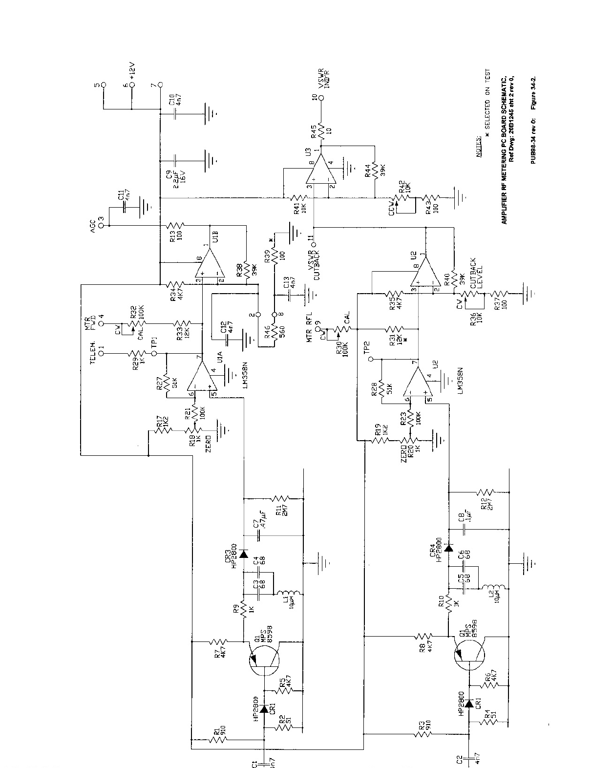
indicates 10% output. This means that in severe VSWR conditions such as in an
open circuit, the amplifier will automatically cuts back to 10% thus protecting
itself.
3. Replace the cables in their proper connections. RFL meter reading should be
nill and the FWD meter reading should be back to 100%. If the FWD reading is much
less than 100%, R36 was probably overadjusted.

Contents:
Sec Topic Page
1 RF Pin Attenuator Board Description.......................................................................34a-1
2 AGC/Overpower Protection Setup ...........................................................................34a-1
List of Figures:
Fig Title Drawing Reference
1 Pin Attenuator Board Assembly.....................................................................10A1255G1
2 Pin Attenuator Board Schematic........................................................................20B1287
1. RF Pin Attenuator Board 10A1255G1: Figures 1 and 2.
(Refer also to the RF Metering Board section of this manual)
The function of this board is to limit the output power of the amplifier to about 110% for up to 3dB increase of
input power. The Pin Attenuator Board acts as a variable attenuator controlling the input level to the pre-amplifier
for AGC and cutback purposes. Operational amplifier U2B controls the amount of attenuation in the circuit.
Three inputs are summed at pin 6 from the VSWR and AGC circuits and additionally from U2A which is a
"mute" type signal. R5 controls the threshold of these signals. The circuit configuration comprising CR1, CR2
and CR3 form a matched attenuator, biased by the output of U2B, R2, R3, R7 and R8. As the output of U2B
lowers due to a voltage increase of one (or more) of the three inputs, the attenuation of the circuit increases,
thus decreasing the RF output at J2.
2. AGC/Overpower protection setup
1. Adjust R5 on the Pin Attenuator Board fully clockwise (minimum attenuation).
2. Adjust the input power from the exciter or channel processor for an output power of about 110% (11Wsp).
3. Adjust R5 on the Pin Attenuator board CCW (counter-clockwise) for the output power to just starts to drop,
say by 5%. This adjustment sets the threshold and corresponds to a dc voltage of about 6V at U2 pin 7 of the
Pin Attenuator Board. Check that this is so.
Readjust power to 110% using the output level control in the exciter or channel processor.
4. Next, adjust potentiometer R39 on the RF METERING BOARD for the output to drop to 100%. This sets the
overpower protection limit to 100%.
5. Verify AGC/Overpower protection operation by increasing the input to the amplifer by about 3dB using the
exciter or channel processor control. The output of the amplifier should not increase by more than 10%.
6. Reduce the level of the exciter or channel processor so that the amplifier output is back to 100%.
NOTE: The procedure described above is valid if on the RF METERING BOARD R46 is 100 Ohms, and R39 is
a 1k potentiometer. In earlier versions R46 is 430-560 Ohms, and R39 is a 100 Ohm fixed resistor. If you have
Comment: The footer date stamp
must agree with the revision
date.