Larcan MXI030U Digital Television Broadcast Translator User Manual Heading 3
Larcan Inc Digital Television Broadcast Translator Heading 3
Larcan >
user manual

TSM20-378
MXi030U AMPLIFIER
TECHNICAL SERVICE MANUAL
LARCAN INC.
228 AMBASSADOR DRIVE
MISSISSAUGA, ONTARIO
CANADA L5T 2J2
PHONE: (905) 564-9222
FAX: (905) 564-9244
EMAIL: techservices@larcan.com
PUBLICATION TSM20-378 Rev 0
July 18, 2007
MXi030U TECHNICAL SERVICE MANUAL
TSM20-378 MXi030U TECHNICAL SERVICE MANUAL
CONTENTS
1 INTRODUCTION .............................................................................................................................................................1
2 SAFETY NOTICES...........................................................................................................................................................2
2.1 BERYLLIUM OXIDE WARNING ......................................................................................................................................2
2.2 OTHER TOXIC MATERIALS ...........................................................................................................................................2
2.3 DANGEROUS VOLTAGES...............................................................................................................................................2
2.3.1 Switch to Safety....................................................................................................................................................3
3 LARCAN PARTS, ASSEMBLIES, ASSEMBLY DRAWINGS AND SCHEMATIC NUMBERS............................5
3.1 VENDOR STANDARD PART NUMBERS...........................................................................................................................5
3.2 LARCAN NUMBERS FOR PARTS, ASSEMBLIES AND DOCUMENTATION .......................................................................5
3.3 LEADED RESISTORS......................................................................................................................................................6
3.4 SURFACE MOUNT RESISTORS 1/4W AND LESS .............................................................................................................6
3.5 SURFACE MOUNT CAPACITORS ....................................................................................................................................7
3.6 PARTS LISTS .................................................................................................................................................................7
3.6.1 Production Changes.............................................................................................................................................7
4 GLOSSARY .......................................................................................................................................................................9
PUB07-03 MXi HALF PALLET OPERATIONS AND MAINTENANCE
1 MXi AMPLIFIER..............................................................................................................................................................1
2 MXi CONTROLLER ........................................................................................................................................................2
3 AMPLIFIER INSTALLATION AND STARTUP..........................................................................................................4
3.1 BEFORE APPLYING AC TO THE UNIT ............................................................................................................................4
3.2 APPLYING AC TO THE UNIT..........................................................................................................................................4
3.3 BEFORE TURNING THE AMPLIFIER ON .........................................................................................................................5
3.4 AMPLIFIER ON SEQUENCE............................................................................................................................................6
3.4.1 Turning ON MXi Amplifier ..................................................................................................................................6
4 TEST AND TROUBLESHOOTING ...............................................................................................................................7
4.1 BENCH TEST PROCEDURES ...........................................................................................................................................7
4.1.1 Front-End Module Bench Test Procedure...........................................................................................................7
4.1.2 IPA1 Bench Test Procedure.................................................................................................................................7
4.1.3 PA Pallet 21B1751 Bench Test Procedure ..........................................................................................................8
4.2 BASIC TROUBLESHOOTING TECHNIQUES ......................................................................................................................8
4.2.1 Amplifier Completely OFF...................................................................................................................................8
4.2.2 No RF Output.......................................................................................................................................................8
4.2.3 Output Reduced to 25%.......................................................................................................................................8
5 MAINTENANCE...............................................................................................................................................................9
5.1 DAILY...........................................................................................................................................................................9
5.2 MONTHLY.....................................................................................................................................................................9
5.3 SEMI-ANNUALLY AND ANNUALLY ...............................................................................................................................9
6 SERVICE..........................................................................................................................................................................10
6.1 REMOVING THE FAN ARRAY.......................................................................................................................................10
6.2 REPLACING THE ENTIRE FAN ARRAY .........................................................................................................................11
6.3 REPLACING A SINGLE FAN..........................................................................................................................................11
TSM20-378 Rev 0 July 18, 2007 20-378-ii MXi030U Technical Service Manual
MXi030U TECHNICAL SERVICE MANUAL
7 TEST EQUIPMENT SETUP..........................................................................................................................................12
8 SPECIFICATIONS .........................................................................................................................................................13
8.1 ELECTRICAL ...............................................................................................................................................................13
8.2 ENVIRONMENTAL .......................................................................................................................................................13
8.3 COOLING ....................................................................................................................................................................13
8.4 DIMENSIONS ...............................................................................................................................................................13
8.5 SHIPPING WEIGHT ......................................................................................................................................................13
PUB07-04 MXi HALF PALLET AMPLIFIER CHASSIS
1 MXi HALF PALLET AMPLIFIER.................................................................................................................................1
PUB07-05 MXi HALF PALLET AMPLIFIER HEATSINK ASSEMBLY
1 HEATSINK ASSEMBLY 40D2052G1.............................................................................................................................1
2 FRONT END MODULE ASSEMBLY 21B1473G1........................................................................................................2
3 IPA MODULE 21B1951G1...............................................................................................................................................3
4 PA PALLET ASSEMBLY 21B1751G1............................................................................................................................5
5 DIRECTIONAL COUPLER 10A2121G3 .......................................................................................................................6
PUB05-67 MXi 500W POWER SUPPLY
1 MXi 500W POWER SUPPLY LAR500-32-P5337..........................................................................................................1
2 POWER SUPPLY MANUAL REPRINT........................................................................................................................3
PUB06-82 Rev2 MXi CONTROLLER BOARD
1 INTRODUCTION .............................................................................................................................................................1
2 GENERAL OPERATIONS ..............................................................................................................................................3
2.1 CONNECTOR AND SIGNAL DEFINITIONS........................................................................................................................3
2.1.1 J1 BDM (Background Debug Mode) Connection................................................................................................3
2.1.2 J2 Remote RS232 Connection..............................................................................................................................3
2.1.3 J3 Front Panel LCD and Touchpad.....................................................................................................................3
2.1.4 J4 +28 Volt DC Power Supply.............................................................................................................................3
2.1.5 J5 +28 Volt DC Power Supply Sensing (External)..............................................................................................3
2.1.6 J6 Remote Controls..............................................................................................................................................3
2.1.7 J7 Transmitter Switch Interface...........................................................................................................................4
2.1.8 J8 Fan Interface...................................................................................................................................................4
2.1.9 J9 External Controls............................................................................................................................................4
2.1.10 J10 AGC Control .................................................................................................................................................4
2.1.11 J11 Aural Detector (Optional).............................................................................................................................4
2.1.12 J12 Forward RF Sample......................................................................................................................................4
2.1.13 J13 Reflected RF Sample .....................................................................................................................................4
2.1.14 J14 Front Panel LCD Power ...............................................................................................................................4
TSM20-378 Rev 0 July 18, 2007 20-378-iii MXi030U Technical Service Manual
MXi030U TECHNICAL SERVICE MANUAL
2.2 JUMPER OPTIONS..........................................................................................................................................................4
2.2.1 BDM Slide Switch S2 ...........................................................................................................................................4
2.3 FRONT PANEL AND CONTROL INDICATORS...................................................................................................................7
2.3.1 Default/Normal E5= Ext E7=Out........................................................................................................................7
2.3.2 Manual Override E5= Int E7=Out......................................................................................................................7
2.3.3 Remote Override E5= Ext E7=In ........................................................................................................................7
2.3.4 Manual and Remote Override E5= Int E7=In.....................................................................................................7
2.4 RF DETECTOR OPERATION ...........................................................................................................................................8
2.5 AGC, VSWR AND CUTBACK OPERATION ....................................................................................................................9
2.6 INTERLOCKS ...............................................................................................................................................................10
2.6.1 Hard Interlocks..................................................................................................................................................10
2.6.2 Soft Interlocks ....................................................................................................................................................11
2.7 EXTERNAL SIGNALS AND REMOTE CONTROL.............................................................................................................11
2.7.1 External #1 Interlock .........................................................................................................................................11
2.7.2 Remote Controls (Individual).............................................................................................................................12
2.7.3 Remote Interface (Serial)...................................................................................................................................12
2.7.4 Transmitter Switching Interface.........................................................................................................................12
2.7.5 External DC Power Supply................................................................................................................................12
3 LCD GUI INTERFACE AND TOUCHPAD.................................................................................................................13
3.1 MAIN SCREEN AND TOUCHPAD OPERATIONS .............................................................................................................13
3.1.1 REM...................................................................................................................................................................14
3.1.2 AGC ...................................................................................................................................................................14
3.1.3 ERR....................................................................................................................................................................14
3.1.4 LOG ...................................................................................................................................................................14
3.1.5 AMP...................................................................................................................................................................15
3.1.6 P/S......................................................................................................................................................................15
3.1.7 INTK ..................................................................................................................................................................15
3.1.8 GEN ...................................................................................................................................................................15
3.2 AMPLIFIER SCREEN ....................................................................................................................................................15
3.2.1 TRIP...................................................................................................................................................................17
3.2.2 L/O.....................................................................................................................................................................17
3.2.3 RF ......................................................................................................................................................................17
3.2.4 INTK ..................................................................................................................................................................17
3.2.5 PSOK .................................................................................................................................................................17
3.2.6 FAN1..................................................................................................................................................................17
3.2.7 FAN2..................................................................................................................................................................18
3.3 POWER SUPPLY SCREEN .............................................................................................................................................19
3.3.1 OK STAT............................................................................................................................................................19
3.3.2 PS ON ................................................................................................................................................................19
3.3.3 INTK ..................................................................................................................................................................19
3.3.4 FAN....................................................................................................................................................................19
3.4 INTERLOCKS SCREEN..................................................................................................................................................19
3.4.1 TRIP...................................................................................................................................................................20
3.4.2 L/O.....................................................................................................................................................................21
3.4.3 TEMP.................................................................................................................................................................21
3.4.4 PSOK .................................................................................................................................................................21
3.4.5 VOR....................................................................................................................................................................21
3.4.6 CUTB.................................................................................................................................................................21
3.4.7 FANS..................................................................................................................................................................21
3.5 REMOTE CONTROLS AND RS232 SERIAL SCREEN.......................................................................................................22
3.5.1 Remote ...............................................................................................................................................................23
3.5.2 NewFmt..............................................................................................................................................................23
3.5.3 ExtCmd ..............................................................................................................................................................23
3.5.4 SerCmd ..............................................................................................................................................................23
3.5.5 Error ..................................................................................................................................................................24
3.5.6 Logs Screen........................................................................................................................................................24
TSM20-378 Rev 0 July 18, 2007 20-378-iv MXi030U Technical Service Manual
MXi030U TECHNICAL SERVICE MANUAL
3.6 GENERAL SCREEN ......................................................................................................................................................25
4 SETUP PROCEDURES..................................................................................................................................................27
4.1 RF DETECTOR ............................................................................................................................................................27
4.2 AGC AND CUTBACK PROTECTION..............................................................................................................................29
4.2.1 AGC Setup..........................................................................................................................................................29
4.2.2 Cutback Setup ....................................................................................................................................................29
4.3 VSWR PROTECTION...................................................................................................................................................29
4.4 REMOTE CONTROL INTERFACE BAUD ........................................................................................................................30
4.5 POWER SUPPLY VOLTAGE AND CURRENT CALIBRATION............................................................................................31
5 REMOTE CONTROL CONNECTIONS MXi TRANSMITTER...............................................................................32
5.1 REMOTE CONTROLS....................................................................................................................................................32
5.1.1 RC_TX_On Remote Transmitter ON Control ....................................................................................................33
5.1.2 RC_TX_Off Remote Transmitter OFF Control..................................................................................................33
5.1.3 RC_TX_VOR Remote Transmitter VOR Control ...............................................................................................34
5.1.4 RC_RESET Remote RESET Control..................................................................................................................34
5.2 EXT1 SECONDARY EXTERNAL #1 INTERLOCK ...........................................................................................................34
5.2.1 Status Outputs....................................................................................................................................................35
5.3 TELEMETRY OUTPUTS ................................................................................................................................................35
6 CIRCUIT DESCRIPTIONS...........................................................................................................................................37
6.1 MC68HC908 MICROPROCESSOR................................................................................................................................37
6.2 POWER SUPPLY VOLTAGE AND CURRENT MONITORING ............................................................................................38
6.3 ON/OFF RELAY K1....................................................................................................................................................40
6.4 AGC, CUTBACK AND VSWR....................................................................................................................................40
6.5 SPI UART..................................................................................................................................................................41
6.6 SPI NVPOT ...............................................................................................................................................................42
6.7 RF DETECTOR ............................................................................................................................................................42
6.7.1 Circuit Description ............................................................................................................................................42
6.8 J12 CHANNEL – VISUAL FORWARD ............................................................................................................................42
6.9 J13 CHANNEL – REFLECTED .......................................................................................................................................43
6.10 J12 CHANNEL – AURAL FORWARD .............................................................................................................................44
7 ADDENDUMS .................................................................................................................................................................45
7.1 ADDENDUM 1– CDS51405 DISPLAY CONTROLLER....................................................................................................46
7.2 ADDENDUM 2–DUAL DIGITAL POTENTIOMETER WITH EEPROM .............................................................................49
7.3 ADDENDUM 3–SPI/MICROWIRE-COMPATIBLE UART AND +/-15KV ESD-PROTECTED RS-232 TRANSCEIVERS
WITH INTERNAL CAPACITORS.....................................................................................................................................52
7.4 ADDENDUM 4–MC68HC908GTXX DATA SHEET .....................................................................................................55
7.5 ADDENDUM 5– CURRENT TRANSDUCER HXS 20-NP.................................................................................................62
TSM20-378 Rev 0 July 18, 2007 20-378-v MXi030U Technical Service Manual
MXi030U TECHNICAL SERVICE MANUAL
1 INTRODUCTION
This Technical Service Manual contains publications (PUBs) describing the technical details of the MXi030U
amplifier, as well as the overall operating instructions, including the bench test procedures of the amplifier stages
incorporated in this unit. It also covers the transmitter’s start-up operation, and troubleshooting, as well as basic
transmitter maintenance guidelines.
TSM20-378 Rev 0 July 18, 2007 20-378-1 MXi030U Technical Service Manual
MXi030U TECHNICAL SERVICE MANUAL
2
2.1
2.2
2.3
SAFETY NOTICES
This section provides general guidance and information for the operation, maintenance, and service personnel
who are familiar with the hazards of working with high-powered electronic circuits. This manual does not detail all
of the safety precautions which should be observed when servicing this or any other electronic equipment.
Service by inadequately trained or inexperienced personnel can result in personal injury or death and/or
damage to the equipment.
Important: All personnel concerned with the servicing of this equipment should be thoroughly familiar with
standard first aid procedures for the treatment of electrical burns and shock, including cardio-pulmonary
resuscitation (CPR).
Use the “buddy” system, with one person performing the actual service and a colleague observing. The observer
must be familiar with the work being performed and within sight and sound of the person doing the work. The
observer should not be engaged in any other work or be otherwise distracted; he must be available instantly in
case of accident.
Always have the observer with you when you work on the transmitter.
BERYLLIUM OXIDE WARNING
Internal thermal management in certain RF devices in this equipment is accomplished through the use of
Beryllium Oxide ceramic material. Do not break open any RF power transistors, or otherwise dismantle them.
Beryllium Oxide is a hard white ceramic used as insulation for heatsinking of RF power semiconductors. Beryllium
Oxide is a poison. In case of accidental breakage of devices, do not inhale the resulting beryllium dust and
avoid getting beryllium dust in your mouth. Do not let beryllium into your blood stream through cuts or
open wounds. Seek immediate medical attention if the dust enters your body in any manner. Avoid cuts by
wearing gloves while picking up the broken pieces. Be careful – do not inhale dust while replacing or emptying
vacuum cleaner filter bags and wash your hands thoroughly afterward. Wash your hands thoroughly after
replacing RF power devices. Dispose of defective RF power devices only through approved toxic waste facilities.
Wear gloves when picking up the pieces. Wash your hands thoroughly after replacing devices. Dispose of defective
devices only through approved toxic waste facilities.
When cleaning up after an accidental breakage, remember to wear a respirator mask to avoid inhaling the dust while
replacing or emptying vacuum cleaner filter bags and to wash your hands well after servicing the vacuum cleaner. If
possible, use a wet vacuum, in which the dust gets trapped in water.
OTHER TOXIC MATERIALS
The non-metallic coverings of some coaxial cables used in this equipment are flammable and can transmit fire
when ignited. Other wire coverings are not capable of supporting combustion but any non-metallic covering when
heated sufficiently can emit dense smoke and acid gases, which can be highly toxic and often corrosive.
Solvents and glues can emit toxic vapors and can be flammable. Read and understand the directions on the
containers and ensure that they are used only in well ventilated locations.
DANGEROUS VOLTAGES
This equipment has been designed to protect operating personnel from accidental contact with dangerous voltages,
by means of shields and covers. It is extremely important that any protective covering devices be kept in place at all
times.
While all practical safety precautions have been adopted to safeguard personnel from possible injury, both
supervisory and operating personnel are urged to ensure that the safety rules detailed below are followed as an
established routine at all times. The following four Rules are the standard safety guidelines for working with and
around transmitters.
TSM20-378 Rev 0 July 18, 2007 20-378-2 MXi030U Technical Service Manual
MXi030U TECHNICAL SERVICE MANUAL
Rule #1 KILL THE AC POWER BEFORE IT KILLS YOU
Under no circumstances should any person reach within the cabinets for the purpose of servicing or
adjusting the equipment without first disconnecting the AC power or without the immediate presence of
another person capable of rendering aid. The “buddy” system is encouraged for transmitter work.
Rule #2 DO NOT TAMPER WITH INTERLOCKS OR SAFETY SHIELDS
Under normal circumstances, no safety shield should be removed.
Rule #3 REMOVE PERSONAL JEWELRY WHEN WORKING ON THE EQUIPMENT
The mains AC power to this transmitter can deliver high currents capable of melting metallic tools or
personal jewelry, such as watch bands, bracelets, or rings. Accidental short circuits from such metallic
objects can cause an explosive shower of molten metal which can result in serious personal injury.
Rule #4 KNOW FIRST AID AND KEEP FIRST AID SUPPLIES AVAILABLE
Illustrated first aid instructions for the treatment of electrical shock and burns and CPR procedures should
be displayed in a prominent location adjacent to the equipment. In rendering first aid, the timeliness and
effectiveness of the treatment are vitally important to the recovery of the injured person.
Always have a colleague with you when you work on the transmitter and make sure both of you know first
aid, including cardio-pulmonary resuscitation (CPR). This is most important.
Without exception, all personnel should thoroughly familiarize themselves with the procedures involved. One
person, whose normal duties place him or her at the transmitter site often, should be given complete
responsibility and authority to ensure that first aid supplies are kept onsite and maintained. Prominently
display a list of emergency phone numbers. This list should include the numbers of the nearest police,
ambulance, hospital, doctor, fire department, paramedics, poison control center, public works (roads)
department, and the utility (power and phone) companies.
Do not try to work on the transmitter if you are tired or drowsy; you could make a fatal error in judgment.
2.3.1 Switch to Safety
Here are some safety suggestions, based partially on the knowledge of experts familiar with high-powered tubed
equipment, and partially on the procedures used at a typical utility company and at a company which makes and
tests high voltage devices. A few of these suggestions apply primarily to factory environments and require some
modification to be applied in transmitter settings.
Our thanks to the Varian Corporation for sharing its "Electrical Safety Training Program" notes. Our thanks also to
Ontario Hydro for its information booklets dealing with high voltage.
Have in place a comprehensive safety program, with defined procedures. Know First Aid and CPR.
Use the “buddy” system, with one person performing the actual service and a colleague observing. The observer
must be familiar with the work being performed and within sight and sound of the person doing the work. The
observer should not be engaged in any other work or be otherwise distracted; he must be available instantly in
case of accident. Always have the observer with you when you work on the transmitter.
Pay attention to emergency communications requirements. This could even include a voice channel on the STL
so that constant communication with the studio can be maintained. Headset-equipped phones connected on this
voice channel should be installed in locations near hazardous areas or everyone on site should carry fully
charged cell phones. When you are administering CPR, you might not be able to leave your patient for the length
of time it could take to call paramedics, especially if phone service is poor, or lines are down, and/or you are in a
rural area without emergency telephone service (e.g., 911 in North America).
Do not defeat the interlock switches on access doors unless it is absolutely necessary and you know exactly
what you are doing.
Keep the area neat and tidy, free of any interfering conductive material and free of any sharp objects. Remember
that reaction to a shock could cause you to strike nearby objects.
TSM20-378 Rev 0 July 18, 2007 20-378-3 MXi030U Technical Service Manual
MXi030U TECHNICAL SERVICE MANUAL
Avoid wearing loose clothing and personal jewelry such as rings, watches, and chains when working near
energized circuits. Make a habit of removing all jewelry and storing it in a safe place as soon as you enter the
transmitter building.
Before beginning work, shut off all AC to the transmitter power supplies. Tag and lockout the switches.
Your safety routine must ensure that the person placing the tag and locking the switch is the only person who
removes it and reactivates the switch. You might want to include the AC to the remote control as well, if there is
any possibility that a studio worker could unknowingly activate the transmitter while you are working on it. One
way of ensuring that the lockout "placer and remover" are the same person is to issue individual padlocks to each
person on the transmitter technical staff.
You might want to include your tower contractor's rigging crew in the list of people who are allowed to use tags
and padlocks. As an alternative, Dielectric™ makes a transmission line lockout switch that is intended for riggers
to turn off and lock out any RF before climbing over the antenna to replace light bulbs, etc.
Proper grounding is vital. Make ground inspection a part of your maintenance program; someone's life could
depend on it.
TSM20-378 Rev 0 July 18, 2007 20-378-4 MXi030U Technical Service Manual
MXi030U TECHNICAL SERVICE MANUAL
3
3.1
3.2
LARCAN PARTS, ASSEMBLIES, ASSEMBLY DRAWINGS AND SCHEMATIC
NUMBERS
VENDOR STANDARD PART NUMBERS
Vendor or original manufacturer part numbers are indicated for most components.
LARCAN NUMBERS FOR PARTS, ASSEMBLIES AND DOCUMENTATION
An index of LARCAN specified number are used to define and specify the following:
• parts made by a manufacturer to LARCAN specification;
• an assembled unit or “group” such as a PC Board or completed cabinet;
• assembly drawings and schematics;
• standards.
Depending on the application, AutoCAD drawing or Microsoft Word document format is used.
Document numbers have the format YYZXXXXKn Rev m where:
YYZ Prefix denoting drawing size and Product type. Can be 10A, 11A, 20B, 21B, 30C, 31C, 40D, 41D, 50E, 51E
– describes drawing or document size, VHF or UHF application
XXXX Drawing Index number. Between 0000 to 9999.
K Refers to the type of drawing / document:
• “no suffix” for drawing of part (assembly or schematic)
• P = Part
• G = Group of parts
• A = Assembly drawing
• F = PC board fabrication films and
• S = Schematic
n Index number for drawing type. Part, group, assembly drawing or schematic next number and may be
one or more digits
Rev Revision (sometimes denoted as R or R–)
m Revision number and may be one digit or more. May contain a decimal (e.g., Revision 3.2)
Drawings may consist of one or more sheets. Generally multiple sheets are used if one sheet is not enough to
show all necessary information. Sometimes, especially with older drawings, multiple sheets are used to show
more than one part or assembly.
TSM20-378 Rev 0 July 18, 2007 20-378-5 MXi030U Technical Service Manual
MXi030U TECHNICAL SERVICE MANUAL
3.3 LEADED RESISTORS
Generic carbon composition resistors with leads are numbered as follows:
3R P
nnnx
- or -
nnx
Power Rating Resistance Value * Tolerance
152 = 1/4W nn - first digits of K =10%
77 = 1/2W resistance (5, 10% tol.) J =5%
78 = 1W nnn - first digits of H =1%
79 = 2W resistance (1% tol.)
x - x10 multiplier
For values between 1Ω and 10Ω, a letter “R” will appear in the resistance value to indicate the decimal place.
For vendor leaded resistors a generic drawing describing basic specifications, but having many “parts”, will often
be used.
“3R152P5R6J” is 5.6Ω, 1/4W, ±5%
“3R152P470K” is 47Ω, 1/4W, ±10%
“3R152P1022H” is 10.2kΩ, 1/4W, ±1%
“3R152P102J” is 1kΩ, 1/4W, ±5%
3.4 SURFACE MOUNT RESISTORS 1/4W AND LESS
There is no specified recommended supplier of these parts. The Philips numbering system is employed with the
following parameters/designations (example follows):
9C A nnnx
SIZE LxW POWER
RATING RESISTANCE VALUE TOLERANCE TEMP COEF
0603=1.6x08mm 1 = 1/16W nnx tolerance>=5% D=0.5% C=50ppm/°C
nn=first 2 digits
x=multiplier F=1% K=100ppm/°C
0805=2x1.25mm 2 = 1/10W
nnnx tolerance<5% J=5% L=200ppm/°C
nnn=first 3 digits
1206=3.2x1.6mm 2 = 1/8W
(1% tol.)
x=multiplier M=300ppm/°C
3 =1/4W
(5% tol.)
nRnx or nnRnx or nRnnx
R inserted as decimal point
where required
0000 - four zeros for jumper
The pairs of parameters enclosed in boxes are normally mutually selected; for example, a resistor having 1%
tolerance normally is selected as having a temperature coefficient of 100ppm/°C.
TSM20-378 Rev 0 July 18, 2007 20-378-6 MXi030U Technical Service Manual

MXi030U TECHNICAL SERVICE MANUAL
Example: 9C08052A1001FK
(Size 0805, Power Rating 1/10W, Resistance 1kohm, Tolerance 1%, Temperature
Coefficient 100ppm/°C)
3.5 SURFACE MOUNT CAPACITORS
There is no specifically recommended supplier of these parts. The part numbering system being used is based on
a Philips (now Yageo/Phycomp) numbering system with the following parameters/designations (example follows):
Nnx
SIZE LxW DIELECTRIC
MATERIAL CAPACITANCE
VALUE
(in Pico farads)
TOLERANCE VOLTAGE
RATING TERMINATION
0603=1.6x08mm CG = NPO nn =first 2 digits B=0.10pF 7=16VDC B=Ni/Sn
0805=2x1.25mm 2R = X7R C=0.25pF 8=25VDC A=Ag/Pd
1206=3.2x1.6mm 2F = Y5V * x =multiplier as
shown below
D=0.50pF 9=50 VDC C=Ni/Sn-Pb
2E = Z5U * 8=x0.01
F=1% 0=100VDC
9=x0.1
G=2% B=200VDC
0=x1
J=5% D=500VDC
1=x10
K=10%
2=x100
M=20%
3=x1000
4=x10000
5=x100000
* (infrequent use)
e.g., 0805CG102J9B
SIZE =0805
DIELECTRIC MATERIAL =NPO
VALUE =1000pF
TOLERANCE =5%
VOLTAGE RATING =50V
TERMINATION =Ni/Sn
PACKAGING =Not Specified
MARKING =None
Note that “u” appears in most cases instead of the correct symbol “μ” whenever a “micro” is required. Electronic
parts list data, when imported by our PC publication program, allows us to substitute the correct “μ” when
checking and editing.
3.6
3.6.1
PARTS LISTS
Parts lists for all assemblies in the transmitter are provided on CD-ROM, in PDF format. The CD-ROM is packed
inside the transmitter cabinet for shipping.
Parts lists are generated in a hierarchical structure, beginning with major assemblies, then the subassemblies of
each major assembly, and so forth.
Production Changes
From time to time, it may become necessary to make changes in the equipment described in this manual. Such
changes are usually made either to provide improved performance or to accommodate component substitutions.
TSM20-378 Rev 0 July 18, 2007 20-378-7 MXi030U Technical Service Manual
MXi030U TECHNICAL SERVICE MANUAL
A revision letter or number may follow the model or group number marked on the nameplate, chassis, or circuit
board; or on the parts list (where it is an "R" followed by a dash and a number). Whenever a revision letter or
number appears, it should be quoted in any communication regarding the equipment.
TSM20-378 Rev 0 July 18, 2007 20-378-8 MXi030U Technical Service Manual

MXi030U TECHNICAL SERVICE MANUAL
4 GLOSSARY
The following glossary lists terms and abbreviations found in this and other LARCAN documentation.
REFERENCE DESIGNATOR ABBREVIATION DESCRIPTION
ADJ ADJUSTMENT/ADJUSTABLE
ALT ALTERNATE
AC ALTERNATING CURRENT
AWG AMERICAN WIRE GAUGE
AMP AMPLIFIER
AM AMPLITUDE MODULATION
ANA ANALOG
ADC ANALOG DIGITAL CONVERTER
E ANT ANTENNA
DS APHANUMERIC DISPLAY
ALU ARITHMETIC LOGIC UNIT
ARM ARMING
ASYNC ASYNCHRONOUS
AT ATT ATTENUATOR
LS AUDIBLE ALARM
AF AUDIO FREQUENCY
AUR AURAL
AUTO AUTOMATIC
AFC AUTOMATIC FREQUENCY CONTROL
AGC AUTOMATIC GAIN CONTROL
ALC AUTOMATIC LEVEL CONTROL
T AUTOTRANSFORMER
AVG AVERAGE
BNC BAYONET NEILL CONCELMAN CONNECTOR
BGA BALL GRID ARRAY
Z BALUN
BPF BANDPASS FILTER
BT BAT BATTERY
BZL BEZEL
BCD BINARY CODED DECIMAL
BCMOS BIPOLAR COMPLIMENTARY MOS
BLK BLOCK
B BLOWER
BRD BOARD
BTM BOTTOM
BKT BRACKET
W BUS BAR
BSHG BUSHING
LS BUZZER
CAB CABINET
W CBL CABLE
C CAP CAPACITOR
CATH CATHODE
CRT CATHODE RAY TUBE
CT CENTER TAP
CPU CENTRAL PROCESSING UNIT
CTR CENTRE
CER CERAMIC
CHAM CHAMFER
CHAN CHANNEL
CHAS CHASSIS
CB CB CIRCUIT BREAKER
HY CIRCULATOR
CLR CLEAR, CLEARANCE
M CLOCK
CW CLOCKWISE
COAX COAXIAL
L COIL
CMB COMBINE
TSM20-378 Rev 0 July 18, 2007 20-378-9 MXi030U Technical Service Manual

MXi030U TECHNICAL SERVICE MANUAL
CMOS COMPLIMENTARY METAL OXIDE
SEMICONDUCTOR
J CONN CONNECTOR
K CONTACTOR (MAGNETICALLY OPERATED)
S CONTACTOR
(MANUALLY, MECHANICALLY, THERMALLY
OPERATED)
CW CONTINUOUS WAVE
CTRL/CTL CONTROL
CLG COOLING
CORR CORRECTION
CCW COUNTERCLOCKWISE
CPLR COUPLER
B/CPLR COUPLER BI-DIRECTIONAL
D/CPLR COUPLER DIRECTIONAL
COV COVER
Y XTAL CRYSTAL
CR CURRENT REGULATOR
DEFL DEFLECTOR
DL DELAY LINE
DEMUX DEMULTIPLEXER
DET DETECTOR
DIFF DIFFERENTIAL
DIG DIGITAL
DAC DIGITAL ANALOG CONVERTER
DPM DIGITAL PANEL METER
D DIODE
DIPL DIPLEXED
DDS DIRECT DIGITAL SYNTHESIS
DMA DIRECT MEMORY ACCESS
DC DIRECTIONAL COUPLER
P DISCONNECTING DEVICE (PLUG CONNECTOR)
J DISCONNECTING DEVICE (RECEPTACLE
CONNECTOR)
DWG DRAWING
DIP DUAL IN LINE PACKAGE
D/L DUMMY LOAD
DRAM DYNAMIC ACCESS RANDOM MEMORY
ELEC ELECTRIC
E ELECTRICAL CONTACT
S ELECTRICAL SAFETY INTERLOCK
E ELECTRICAL SHIELD
ELECT ELECTROLYTIC (CONTEXT:CAPACITOR)
EMI ELECTROMAGNETIC INTERFERENCE
V ELECTRON TUBE
ELEK ELECTRONIC
LS ELECTRONIC BELL
M ELECTRONIC COUNTER
M ELECTRONIC TIMER
ECL EMITTER COUPLED LOGIC
ENCL ENCLOSURE
EQ EQ EQUALIZER
EXC EXCITER
EXH EXHAUST
EXT EXTERNAL
FFT FAST FOURIER TRANSFORM
FEM FEMALE
FPT FEMALE PIPE THREAD
E FERRITE BEAD RINGS
FET FIELD EFFECT TRANSISTOR
FPGA FIELD PROGRAMMABLE GATE ARRAY
FPLA FIELD PROGRAMMABLE LOGIC ARRAY
FL FILT FILTER
FWD FORWARD
FR FRAME
TSM20-378 Rev 0 July 18, 2007 20-378-10 MXi030U Technical Service Manual

MXi030U TECHNICAL SERVICE MANUAL
FREQ FREQUENCY
FDM FREQUENCY DIVISION MULTIPLEX
FM FREQUENCY MODULATION
FSK FREQUENCY SHIFT KEYING
FR FRONT
F FUSE
X FUSEHOLDER
G GENERATOR
GROM GROMMET
GND GROUND
GRP DEL GROUP DELAY
E HALL ELEMENT
HDL HANDLE
H HARDWARE
J HDR HEADER
HR HEATER
HR HEATING RESISTOR
HTSK HEATSINK
HCMOS HIGH DENSITY CMOS
HMOS HIGH PERFORMANCE MOS
HP HIGH POWER
HCT HIGH SPEED CMOS
HV HIGH VOLTAGE
HPS HIGHPASS FILTER
HORIZ HORIZONTAL
HSG HOUSING
HY HYBRID CIRCUIT NETWORK
ID IDENTIFICATION
E IGNITOR GAP
I INCIDENT
IOT INDUCTIVE OUTPUT TUBE
L IND INDUCTOR
L INDUCTOR
IN, I/P, INP INPUT
INSR, INST INSERT
INS INSIDE
M INSTRUMENT
E INSULATOR
U IC INTEGRATED CIRCUIT
U INTEGRATED CIRCUIT
I/C, INTCON INTERCONNECTION
INTRF INTERFERENCE
INTL INTERLOCK
IF INTERMEDIATE FREQUENCY
INT INTERNAL
ISOL ISOLATION
JFET JUNCTION FET
DS LAMP
LSI LARGE SCALE INTEGRATION
LDMOS LATTERALLY DIFFUSED MOS
LCC LEADED CHIP CARRIER
LCCC LEADLESS CERAMIC CHIP CARRIER
DS LED
LLCC LEADLESS CHIP CARRIER
LED LIGHT EMITTING DIODE
E LIGHTING ARRESTOR
LIN LINEAR
LCD LIQUID CRYSTAL DISPLAY
LOC LOCAL
LAN LOCAL AREA NETWORK
LO LOCAL OSCILLATOR
L/O LOCKOUT
LS LOUDSPEAKER
LNA LOW NOISE AMPLIFIER
TSM20-378 Rev 0 July 18, 2007 20-378-11 MXi030U Technical Service Manual

MXi030U TECHNICAL SERVICE MANUAL
LP LOW POWER
LV LOW VOLTAGE
LWR LOWER
FL LPS LOWPASS FILTER
E MAGNETIC CORE
Vcc MAIN POWER SUPPLY
M MALE
MPT MALE PIPI THREAD
MATL MATERIAL
MP MECHANICAL INTERLOCK
MP MECHANICAL PART
MP MEDIUM POWER
MOS METAL OXIDE SEMICONDUCTOR
MOSFET METAL OXIDE SEMICONDUCTOR FET
MOV METAL OXIDE VARISTOR
MTR METER
M METER
MK MICROPHONE
E MISCELLANUS ELECTRICAL PART
HY MXR MIXER
MOD MODEL
MOD MODULATION
MODEM MODULATOR/DEMODULATOR
MON MONITOR
B MOTOR
MTG MOUNTING
MAC MULTIPLEX ANALOG COMPONENT
MPX MULTIPLEXER
MUX MULTIPLEXER
NMPS N CHANNEL MOS
NEUT NEUTRAL
NONLIN NONLINEAR
NVM NON-VOLATILE MEMORY
NVRAM NON-VOLATILE RAM
OC OPEN COLLECTOR
U OPAMP OPERATIONAL AMPLIFIER
OPT OPTIONAL
OSC OSCILLATOR
G OSCILLATOR
M OSCILLOSCOPE
O/P, OUT OUTPUT
OCXO OVEN CONTROLLED CRYSTAL OSCILLATOR
O/I OVERCURRENT
O/L OVERLOAD
O/V OVERVOLTAGE
PMOS P CHANNEL MOS
PNL PANEL
PPNL PATCH PANEL
E PERMANENT MAGNET
PH PHASE
PLL PHASE LOCKED LOOP
PM PHASE MODULATION
Z PHASE SHIFTER
R POT POTENTIOMETER
RES VAR POTENTIOMETER
R POTENTIOMETER
PWR POWER
PFD POWER FLUX DENSITY
PS POWER SUPPLY
PS POWER SUPPLY
PREAMP PREAMPLIFIER
PFX PREFIX
PREF PREFIX
PRESS PRESSURE
TSM20-378 Rev 0 July 18, 2007 20-378-12 MXi030U Technical Service Manual

MXi030U TECHNICAL SERVICE MANUAL
P PRIMARY
PCA PRINTED CIRCUIT ASSEMBLY
PCBOARD PRINTED CIRCUIT BOARD
PCM PULSE CODE MODULATION
Q QUADRATURE
QAM QUADRATURE AMPLITUDE MODULATION
Y QUARTZ
RU RACK UNIT 1 3/4"
RF RADIO FREQUENCY
RFIC RADIO FREQUENCY INTEGRATED CIRCUIT
RFI RADIO FREQUENCY INTERFERENCE
RAM RANDOM ACCESS MEMORY
ROM READ ONLY MEMORY
RCVR RECEIVER
RX RECEIVING
J RCPTL RECEPTACLE
REF REFERENCE
RFL REFLECTED
REJ REJECT
RL REJECT LOAD
K RLY RELAY
K RELAY
REM REMOTE
R RES RESISTOR
R RESISTOR
Z RESONATOR (TUNED CAVITY)
RND ROUND
SMPL SAMPLE
S SECONDARY
Vdd SECONDARY POWER SUPPLY
SEL SELECT
SCLK SERIAL CLOCK
SIG SIGNAL
SNR SIGNAL TO NOISE RATIO
SCR SILICON CONTROLLED RECTIFIER
SOS SILICON ON SAPPHIRE
SPDT SINGLE POLE DOUBLE THROW
SPST SINGLE POLE SINGLE THROW
SOIC SMALL OUTLINE IC
SOT SMALL OUTLINE TRANSISTOR
SKT SOCKET
X SOCKET
SS SOLID STATE
SND SOUND
E SPARK GAP
SPL SPLITTER
STD STANDARD
STBY STANDBY
SPLY SUPPLY
SPRT SUPPORT
SAW SURFACE ACOUSTIC WAVE
SM SURFACE MOUNT
SMA SURFACE MOUNT ASSEMBLY
SMC SURFACE MOUNT COMPONENT
SMD SURFACE MOUNT DEVICE
SMT SURFACE MOUNT TECHNOLOGY
SW SW SWITCH
S SWITCH
SYNC SYNCHRONIZATION / SYNCHRONOUS /
SYNCHRONISING
SONET SYNCHRONOUS OPTICAL NETWORK
SYS SYSTEM
TANT TANTALUM
TECH TECHNICAL
TV TELEVISION
TSM20-378 Rev 0 July 18, 2007 20-378-13 MXi030U Technical Service Manual

MXi030U TECHNICAL SERVICE MANUAL
TEMP TEMPERATURE
TERM TERMINAL
E TERMINAL (INDIVIDUAL)
TERMBLK TERMINAL BLOCK
TB TERMINAL BLOCK
RT TERMISTOR
TC TERMOCOUPLE
TP TEST POINT
TP TEST POINT
M THERMOMETER
TSSOP THIN SHRINK SMALL OUTLINE PACKAGE
TSOP THIN SMALL OUTLINE PACKAGE
X XFMR TRANSFORMER
T TRANSFORMER
Q TRANSISTOR
TTL TRANSISTOR TRANSISTOR LOGIC
XLTR TRANSLATOR
XMTD TRANSMITTED
XMTR TRANSMITTER
TX TRANSMITTER
TX TRANSMITTER / TRANSMITTING
TRIM TRIMMING
UHF ULTRA HIGH FREQUENCY
UPS UNINTERRUPTABLE POWER SUPPLY
UUT UNIT UNDER TEST
UART UNIVERSAL ASYNCHRONOUS RECEIVER
TRANSMITTER
UPR UPPER
VAR VARIABLE
VGA VARIABLE GAIN AMPLIFIER
D VARISTOR (ASYMETRICAL)
RV VARISTOR (SYMETRICAL)
VERT VERTICAL
VHF VERY HIGH FREQUENCY
VHV VERY HIGH VOLTAGE
VLSI VERY LARGE SCALE INTEGRATION
VIS VISION / VISUAL
VCXO VOLTAGE CONTROLLED CRYSTAL
OSCILLATOR
VCO VOLTAGE CONTROLLED OSCILLATOR
VR VOLTAGE REGULATOR
VR VOLTAGE REGULATOR
W WAVEGUIDE
WLAN WIRELESS LOCAL AREA NETWORK
WRG WIRING
GENERAL
8VSB 8 LEVEL VSB
ATV ADVANCED TELEVISION SYSTEM (U.S.)
ATSC ADVANCED TELEVISION SYSTEMS
COMMITTEE
ACATS ADVISORY COMMITTEE ON ADVANCED
TELEVISION SERVICE
ASCII AMERICAN NATIONAL STANDARD CODE FOR
INFORMATION INTERCHANGE
ANSI AMERICAN NATIONAL STANDARDS INSTITUTE
B&W BLACK AND WHITE
BBC BRITISH BRODCASTING CORPORATION
CATV CABLE TV
CRC COMMUNICATION RESEARCH CENTRE
COMP COMPOSITE
DTTV DIGITAL TERRESTRIAL TV
DVB DIGITAL VIDEO BRODCASTING
EIA ELECTRONICS INDUSTRIES ASSOCIATION
EDTV ENCHANCED DEFINITION TV
ENV ENVELOPE
TSM20-378 Rev 0 July 18, 2007 20-378-14 MXi030U Technical Service Manual

MXi030U TECHNICAL SERVICE MANUAL
EBU EUROPEAN BRODCASTING UNION
DVB EUROPEAN DIGITAL TV
FCC FEDERAL COMMUNICATION COMMISSION
GPIB GENERAL PURPOSE INTERFACE BUS
GPS GEOGRAPHIC POSITIONING SYSTEM
HP HEWLETT PACKARD
HDTV HIGH DEFINITION TELEVISION
HD HIGH DENSITY
HTTP HYPERTEXT TRANSFER PROTOCOL
ICPM INCIDENTAL CARRIER PHASE MODULATION
INC INCORPORATED
ISO INDUSTRIAL STANDARDS ORGANIZATION
IEEE INSTITUTE OF ELECTRICAL AND ELECTRONIC
ENGINEERS
IEC INTERNATIONAL ELECTROTECHNICAL
COMMISSION
ISO INTERNATIONAL ORGANIZATION FOR
STANDARDIZATION
OIRT INTERNATIONAL RADIO AND TELEVISION
ORGANISATION
CCIR INTERNATIONAL RADIO CONSULTATIVE
COMMITTEE (NOW ITU-R)
ITU INTERNATIONAL TELECOMMUNICATION UNION
MONO MONOPHONIC
MPEG MOTION PICTURE EXPERTS GROUP
NTSC NATIONAL TELEVISION STANDARD
COMMITTEE
OSHA OCCUPATIONAL SAFETY AND HEALH
ADMINISTRATION
PCS PERSONAL COMMUNICATION SERVICES
PAL PHASE ALTERNATING LINE TELEVISION
STANDARD
PDF PORTABLE DOCUMENT FORMAT
SAT SATELLITE
KuBand SATELLITE TO SATELLITE COMMUNICATION
FREQUENCY
SECAM SEQUENTIAL COULEUR A MEMORIE
SMPTE SOCIETY OF MOTION PICTURE AND
TELEVISION ENGINEERS
SDTV STANDARD DEFINITION TELEVISION
SCC STANDARDS COUNCIL OF CANADA
STEREO STEREOPHONIC
SUBCARR SUBCARRIER
WWW WORLD WIDE WEB
ORGANIZATIONAL DEPARTMENTS, DOCUMENTS, FUNCTIONS
ASSY ASSEMBLY
BOM BILL OF MATERIAL
DA DEVIATION AUTHORIZATION
EA EACH
PL PARTS LIST
PROD PRODUCTION
PRODN PRODUCTION
PUB PUBLICATION
QA QUALITY ASSURANCE
QC QUALITY CONTROL
QM QUALITY MANUAL
REV REVISION NOTICE
RN REVISION NOTICE
SCHEM SCHEMATIC
SCHEM SCHEMATIC
SHT SHEET
TI TECHNICAL INSTRUCTION / TEST
INSTRUCTION
TSM TECHNICAL SERVICE MANUAL
WHSE WAREHOUSE
TSM20-378 Rev 0 July 18, 2007 20-378-15 MXi030U Technical Service Manual

MXi030U TECHNICAL SERVICE MANUAL
TECHNICAL TERMS
AD ANODE
ATM ASYNCHRONOUS TRANSFER MODE
BIN BINARY
CAD COMPUTER AIDED DESIGN
CAE COMPUTER AIDED ENGINEERING
DEC DECIMAL
HEX HEXADECIMAL
IRQ INTERRUPT REQUEST
OCT OCTAL
VSB VESTIGIAL SIDEBAND MODULATION
VM VOLTMETER
UNITS OF MEASURE, MEASUREMENTS, ORDERS OF MAGNITUDE
pico/ p 1.00E-12
nano/ n 1.00E-09
micro/ u 1.00E-06
mili/ m 1.00E-03
kilo/ k 1.00E+03
Mega/ M 1.00E+06
Giga/ G 1.00E+09
Tera/ T 1.00E+12
A AMPERE
ANG ANGLE
APL AVERAGE PICTURE LEVEL
BW BANDWIDTH
BER BIT ERROR RATE
BPS BITS PER SECOND
BTU BRITISH THERMAL UNIT
C/N CARRIER NOISE RATIO
CMRR COMMON MODE REJECTION RATIO
I CURRENT
dB DECIBEL
DEG DEGREE
C DEGREE CELSIUS
F DEGREE FAHRENHEIT
DG DIFFERENTIAL GAIN
DP DIFFERENTIAL PHASE
DC DIRECT CURRENT
ERP EFFECTIVE RADIATED POWER
F FARAD
H HENRY
Hz HERTZ
Z IMPEDANCE
IMD INTERMODULATION DISTORTION
LSB LEAST SIGNIFICANT BIT
MTBF MEAN TIME BETWEEN FAILURES
Mohm MEGAOHM
MSB MOST SIGNIFICANT BIT
PPS PARTS PER MILLION
P-P PEAK TO PEAK
psi POUNDS PER SQUERE INCH
PF POWER FACTOR
PSD POWER SPECTRAL DENSITY
X REACTANCE
RMS ROOT MEAN SQUARE
BAUD SIGNAL EVENTS PER SECOND
SN SIGNAL TO NOISE
TOL TOLERANCE
THD TOTAL HARMONIC DISTORTION
TPO TRANSMITTER POWER OUTOUT
V VOLT
V VOLTAGE
VSWR VOLTAGE STANDING WAVE RATIO
VA VOLTAMPERE
TSM20-378 Rev 0 July 18, 2007 20-378-16 MXi030U Technical Service Manual

MXi030U TECHNICAL SERVICE MANUAL
W WATT
MISCELLANEOUS
ACS ACCESS
BSC BASIC
BLK BLACK
BLU BLUE
BRN BROWN
CARR CARRIAGE
CHNG CHANGE
DCR DECORATIVE
DEV DEVIATION
DOS DISK OPERATING SYSTEM
FAX FACSIMILE
GRY GRAY
GRN GREEN
HEPA HIGH EFFICIENCY PARTICULATE AIR
h HOUR
JPEG JOINT PHOTOGRAPHIC EXPERTS GROUP
MRI MAGNETIC RESONANCE IMAGINARY
MAX MAXIMUM
MIN MINIMUM
MISC MISCELLANEOUS
MOD MODIFICATION
ORN ORANGE
LBS POUNDS
QUOT QUOTATION
R READ
R/W READ/WRITE
REPL REPLACEMENT
S/N SERIAL NUMBER
SPICE SIMULATION PROGRAM WITH INTEGRATED
CIRCUIT EMPHASIS
TEL TELEPHONE
VIO VIOLET
WTR WATER
WHT WHITE
W WITH
W/O WITHOUT
W WRITE
YR YEAR
YEL YELLOW
TSM20-378 Rev 0 July 18, 2007 20-378-17 MXi030U Technical Service Manual
MXi HALF PALLET OPERATIONS AND MAINTENANCE
PUB07-03 Rev 1 July 17, 2007 07-03-i MXi Half Pallet Operations and Maintenance
CONTENTS
1 MXi AMPLIFIER..............................................................................................................................................................1
2 MXi CONTROLLER ........................................................................................................................................................2
3 AMPLIFIER INSTALLATION AND STARTUP..........................................................................................................4
3.1 BEFORE APPLYING AC TO THE UNIT ............................................................................................................................4
3.2 APPLYING AC TO THE UNIT..........................................................................................................................................4
3.3 BEFORE TURNING THE AMPLIFIER ON .........................................................................................................................5
3.4 AMPLIFIER ON SEQUENCE............................................................................................................................................6
3.4.1 Turning ON MXi Amplifier ..................................................................................................................................6
4 TEST AND TROUBLESHOOTING ...............................................................................................................................7
4.1 BENCH TEST PROCEDURES ...........................................................................................................................................7
4.1.1 Front-End Module Bench Test Procedure...........................................................................................................7
4.1.2 IPA1 Bench Test Procedure.................................................................................................................................7
4.1.3 PA Pallet 21B1751 Bench Test Procedure ..........................................................................................................7
4.2 BASIC TROUBLESHOOTING TECHNIQUES ......................................................................................................................8
4.2.1 Amplifier Completely OFF...................................................................................................................................8
4.2.2 No RF Output.......................................................................................................................................................8
4.2.3 Output Reduced to 25%.......................................................................................................................................8
5 MAINTENANCE...............................................................................................................................................................9
5.1 DAILY...........................................................................................................................................................................9
5.2 MONTHLY.....................................................................................................................................................................9
5.3 SEMI-ANNUALLY AND ANNUALLY ...............................................................................................................................9
6 SERVICE..........................................................................................................................................................................10
6.1 REMOVING THE FAN ARRAY.......................................................................................................................................10
6.2 REPLACING THE ENTIRE FAN ARRAY .........................................................................................................................11
6.3 REPLACING A SINGLE FAN..........................................................................................................................................11
7 TEST EQUIPMENT SETUP..........................................................................................................................................12
8 SPECIFICATIONS .........................................................................................................................................................13
8.1 ELECTRICAL ...............................................................................................................................................................13
8.2 ENVIRONMENTAL .......................................................................................................................................................13
8.3 COOLING ....................................................................................................................................................................13
8.4 DIMENSIONS ...............................................................................................................................................................13
8.5 SHIPPING WEIGHT ......................................................................................................................................................13
FIGURES
FIGURE 1 MXI AMPLIFIER HEATSINK ASSEMBLY ........................................................................................................................1
FIGURE 2 MXI CONTROLLER........................................................................................................................................................2
FIGURE 3 MXI FRONT PANEL .......................................................................................................................................................2
FIGURE 4 MAIN MENU SCREEN ....................................................................................................................................................2
FIGURE 5 AMPLIFIER (AMP) SUBMENU .......................................................................................................................................3
FIGURE 6 POWER SUPPLY (P/S) SUBMENU SCREEN......................................................................................................................3
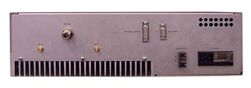
FIGURE 7 REAR PANEL SHOWING INTERLOCK TERMINAL BOARD................................................................................................4
FIGURE 9 MAIN MENU..................................................................................................................................................................5
FIGURE 10 INTERLOCKS STATUS ..................................................................................................................................................5
FIGURE 11 AGC OFF ...................................................................................................................................................................5
FIGURE 12 TRANSMITTER ON ......................................................................................................................................................6
MXi HALF PALLET OPERATIONS AND MAINTENANCE
PUB07-03 Rev 1 July 17, 2007 07-03-ii MXi Half Pallet Operations and Maintenance
FIGURE 13 BOTTOM VIEW OF MXI.............................................................................................................................................10
FIGURE 14 FAN ARRAY ..............................................................................................................................................................10
FIGURE 15 FAN ATTACHMENT TO MOUNTING PLATE.................................................................................................................11
FIGURE 16 TEST EQUIPMENT SETUP...........................................................................................................................................12
MXi HALF PALLET OPERATIONS AND MAINTENANCE
PUB07-03 Rev 1 July 17, 2007 07-03-1 MXi Half Pallet Operations and Maintenance
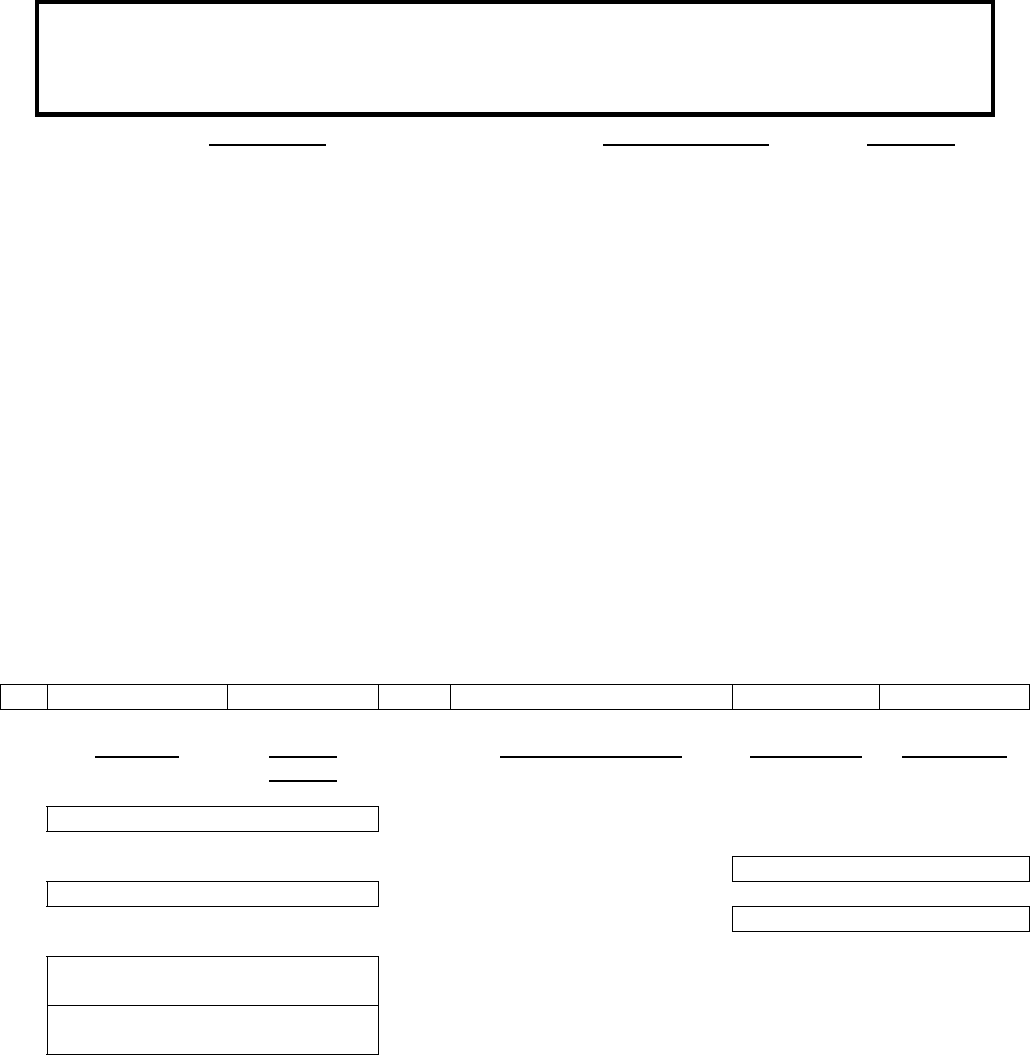
1 MXi AMPLIFIER
The RF section of the MXi Amplifier consists of a heatsink assembly that includes three cascaded broadband
amplifier modules and a directional coupler. Figure 1 shows the layout of this assembly.
Figure 1 MXi Amplifier Heatsink Assembly
Also mounted on the heatsink is a thermal switch that protects the amplifier from over temperature conditions.
MXi HALF PALLET OPERATIONS AND MAINTENANCE
PUB07-03 Rev 1 July 17, 2007 07-03-2 MXi Half Pallet Operations and Maintenance
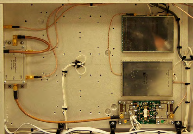
2 MXi CONTROLLER
The MXi control board (Assembly 31C1897) is a single-circuit assembly that provides all of the control functions
required for the MXi series of transmitters on a single circuit board. This board can be configured for a number of
different transmitter types, power levels, transmission standards and options.
Figure 2 MXi Controller
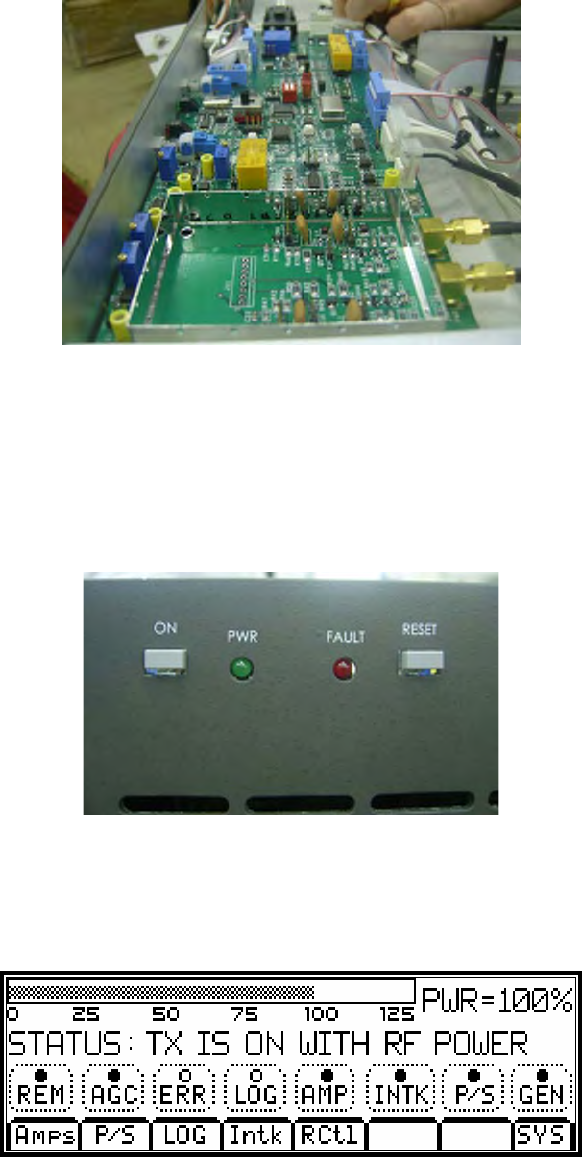
The MXi control board provides local front panel interface via ON/OFF and RESET buttons as well as a graphical
user interface through a front panel LCD assembly with touchpad for user commands. The board implements
controls/status/telemetry for remote control through a rear panel connector that will interface to a typical remote
control systems (such as Moseley or Gentner). An RS232 serial port is also provided to allow the operator to
access the MXi through an external computer (with the appropriate software). The MXi control board has RF
detectors for forward and reflected power and all the circuitry to support AGC/VSWR/Cutback functions. Circuitry
to control and monitor the +32V power supply is also included on this board.
Figure 3 MXi Front Panel
The user interface to the amplifier is accomplished with the front panel LCD that incorporates a touchpad as an
integral part of the unit. The LCD has the capability of displaying a variety of screens, which are selected by the
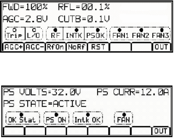
user via the touchpad. Figure 4 shows the LCD main menu, which shows the present status of the amplifier along
with the selections of submenus.
Figure 4 Main Menu Screen
MXi HALF PALLET OPERATIONS AND MAINTENANCE
PUB07-03 Rev 1 July 17, 2007 07-03-3 MXi Half Pallet Operations and Maintenance
Forward (FWD) and Reflected power (RFL), AURal power, AGC and CUTBack (VSWR) control voltage, as well
as the heatsink TEMPerature (Optional) can be displayed by selecting the AMP submenu as shown in Figure 5.
Figure 5 Amplifier (AMP) Submenu
Pressing the power supply ‘P/S’ submenu from the Main Menu will display the power supply voltage and current
consumption as well as its status.
Figure 6 Power Supply (P/S) Submenu Screen
For complete documentation regarding the Controller, see the publication MXi Controller Board.
MXi HALF PALLET OPERATIONS AND MAINTENANCE
PUB07-03 Rev 1 July 17, 2007 07-03-4 MXi Half Pallet Operations and Maintenance
3 AMPLIFIER INSTALLATION AND STARTUP
The MXi Amplifier was fully tested at LARCAN before it was delivered. Under normal circumstances, the
transmitter can be fully operational with minimal setup when turned ON. However, a good practice is to take the
“start from scratch” approach, which means that you should take precautionary measures before the amplifier is
allowed to run at full rated power. These important steps will avoid any catastrophic failures at start-up. The
procedure described is essentially the same approach taken at the factory with a new and untested transmitter.
This also applies if there is a need to completely replace a major sub-assembly in the transmitter.
3.1 BEFORE APPLYING AC TO THE UNIT
Pay careful attention to items 1 to 3 before applying AC to the amplifier. These are initial steps that must be
observed and followed for proper and safe operation of the amplifier.
1. Termination
• Ensure that the amplifier is properly terminated with a suitable load. This can be into a dummy load or into
the transmitter output system. A 50 Ohm, 100W load with at least –20dB return loss (1.2 VSWR) is
recommended. Preferably, directional couplers with known coupling levels at the frequency of interest
should be connected at the input and output of the band-pass filter. These points are very useful in
determining absolute power levels and losses and for use as an RF sample for monitoring purposes. See
Figure 15 for a typical Eclipse transmitter test equipment setup.
2. Interlocks
Antenna or Load interlocks must be connected to the amplifier to avoid damage to the equipment and to the
output section. Interlocking is provided at the INTERLOCK terminal board located on the rear panel. If this
interlock is open, the B+ to the amplifier will shut down, including the cooling fans. DO NOT replace this
interlock with a jumper.
Figure 7 Rear Panel Showing Interlock Terminal Board
3. Power At Minimum
• Initially, the Exciter or Channel Processor’s RF output should be at minimum level. Adjust the OUTPUT
LEVEL control for a minimum output.
3.2 APPLYING AC TO THE UNIT
• Check that the AC voltage available to the amplifier ranges from 90-264VAC. If so, proceed to applying
the power to the AC INPUT of the amplifier
• Once the AC is applied to the unit, the Control Power Supply turns ON and applies +12V to the MXi
Controller.
• Observe that the Power-Up screen is displayed on the LCD, followed by the Main Menu.
MXi HALF PALLET OPERATIONS AND MAINTENANCE
PUB07-03 Rev 1 July 17, 2007 07-03-5 MXi Half Pallet Operations and Maintenance
Figure 8 Main Menu
3.3 BEFORE TURNING THE AMPLIFIER ON
From the Main Menu, the status of the amplifier is displayed and shows if the amplifier is ready for operation.
Status legends, when lit, such as the INTK (INTERLCOK), usually signify OK conditions and that the transmitter is
ready to be turned ON.
Check that all of the following conditions are met:
1. EXCITER or Channel Processor is Ready.
• Usually in the application of AC, the Exciter goes through its warm-up sequence. Ensure that it has done
so.
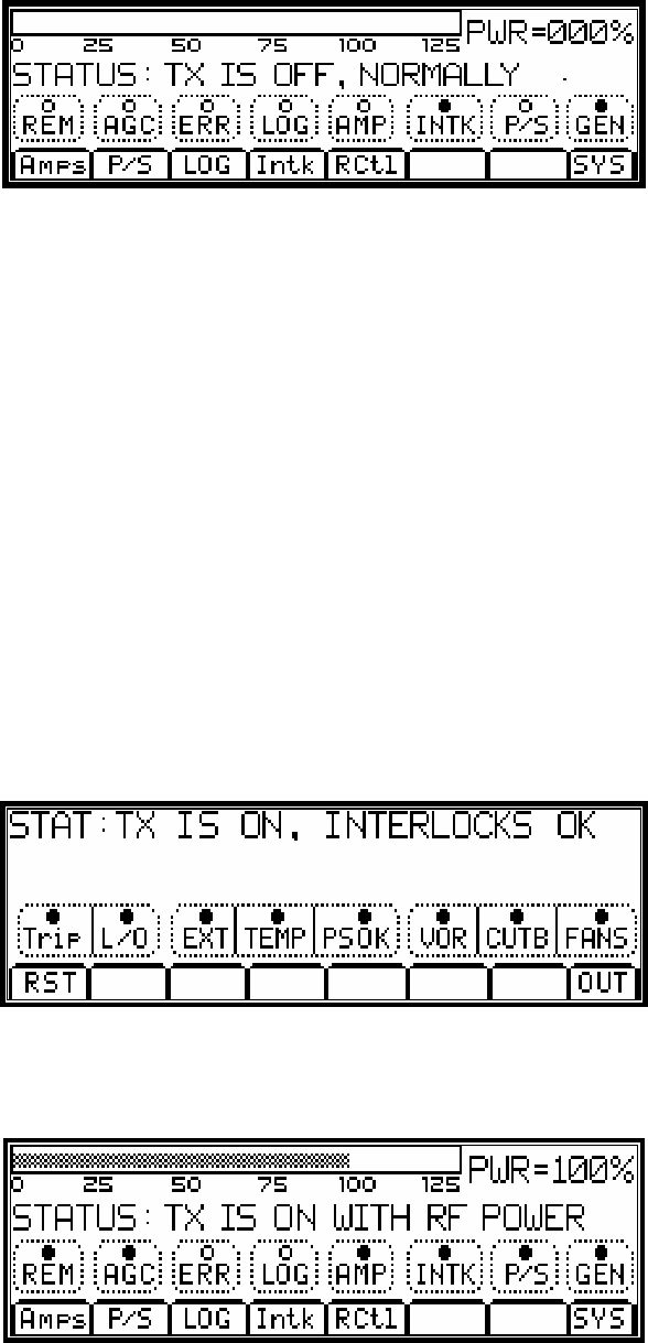
4. POWER METERING is at Zero.
• On the LCD (see Main Menu display in Figure 8), the PWR should be at 000% and the STATUS should
be TX IS OFF, NORMALLY.
5. MXi CONTROLLER is ready.
• If there were prior faults, clear them by pushing the RESET button.
6. INTERLOCKS are closed or OK.
• Interlocks and Status are OK.
Figure 9 Interlocks Status
7. AGC control is DISABLED at this time.
• Push the AGC button on the touchpad so that it is NOT selected.
Figure 10 AGC OFF
8. The Amplifier is in LOCAL mode.
• Push the REM button so that it is not lit.
9. The TX is OFF.
MXi HALF PALLET OPERATIONS AND MAINTENANCE
PUB07-03 Rev 1 July 17, 2007 07-03-6 MXi Half Pallet Operations and Maintenance
• Push the Front Panel ON/OFF button so that it is NOT pushed in.
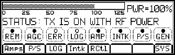
3.4 AMPLIFIER ON SEQUENCE
Upon depressing the ON button, the fans start and at the same time the +32V power supply is enabled, thus
applying B+ to the MXi Amplifier. Since the Exciter or Channel Processor is on hot standby (RF is always
applied), the amplifier normally produces output power immediately.
3.4.1 Turning ON MXi Amplifier
10. Enable amplifier LOCAL operation by pressing the REM touch button such that the REM legend is NOT lit.
• Push the front panel ON button.
• The MXi Amplifier should now be ON.
Figure 11 Transmitter ON
11. Monitor the +32V power supply voltage and current on the LCD screen. Check that the power supply is
operating by pressing the P/S touch button. The voltage reading should be about 32V and the current should
be about 3.3A under Static condition (no RF drive).
ALLOW THE AMPLIFIER SOME WARM-UP TIME!
Only after the transmitter has been ON for approximately 15 minutes should you perform the fine
adjustments. The amplifier must be allowed to reach its operating temperature for stable and consistent
operation. The Power Amplifier in the MXi transmitter is equipped with thermal compensation circuits, which
reduce the output power when the temperature rises. Therefore, the operating temperature must be reached
before adjusting the RF level to its proper level. The amplifier is also equipped with Automatic Gain Control,
primarily designed to prevent the transmitter from overpower or overdrive condition.
12. Increase the RF output by slowly turning the Exciter or Channel Processor output level control.
Stop at about 50% output power indicated on the LCD display. At this level, the current should not be more
than 10 Amps.
13. If the current is not abnormally high, increase the power to 100%. Again, make note of the PS current reading.
This should not be more than 15 Amps.
14. AGC SETTING: With the AGC still disabled, increase the output power to 110%, using the output level control
in the Exciter or Channel processor. Enable the AGC by pressing the AGC touch button until it lights. Use the
LOWER button to set the power to 100%.
15. With the amplifier fully functional and adjusted to its final setting, record keeping becomes very important.
Record the current, voltage, power, etc. This data can be used as a very valuable troubleshooting tool later.
Below is typical test data pertaining to the MXi amplifier at 100% output power.
TYPICAL DATA read on the LCD
FWD 100% CUTB 0.1V
RFL 00.1% PS VOLTS 32.0V
AGC 1.0V PS CURR 12.0A
AUR 100% (Only if running as a analog)

MXi HALF PALLET OPERATIONS AND MAINTENANCE
PUB07-03 Rev 1 July 17, 2007 07-03-7 MXi Half Pallet Operations and Maintenance
4 TEST AND TROUBLESHOOTING
4.1 BENCH TEST PROCEDURES
The following procedures are test instructions for the amplifier modules comprising the MXi amplifier.
4.1.1 Front-End Module Bench Test Procedure
• Connect a +32V (1A current limit) power supply to TP2.
• Apply a 0dBm (1mW) RF input to the amplifier.
• Turn RV2 fully clockwise. The front-end should have a gain of 13dB. Adjusting RV2 from one extreme to
the other should vary the gain by a minimum of 20dB. Set RV2 fully clockwise.
• RF Mute Check: Connect a variable supply to TP1. Gradually increase the voltage until the gain drops by
20dB or more. The applied voltage should be approximately 7 volts.
• Telemetry: Monitor TP3. Note voltage decrease to 0V DC when RF output has been muted.
4.1.2 IPA1 Bench Test Procedure
This amplifier must be mounted on a properly sized heatsink for testing.
• Connect a suitable load to the output of the Pre Amplifier.
• On the unit under test, set RV200 fully clockwise and set RV110 fully counter-clockwise.
• Set variable power supply to 32.0 volts and set its current limit to 1 ampere.
• Apply the +32V to the feedthrough capacitor of the pre-amp shield box.
• Adjust RV3 to achieve 6.5 ±0.2 volts at the junction of R5 and RV100.
• Adjust RV200 to achieve total current draw of 500 ±20 mA.
• Check that the junction of R100 and CR100 measures between 3.5 and 5.5 volts.
• Adjust RV110 to raise total current draw to 1000 ±50 mA.
• Check that the junction of R110 and CR110 measures between 3.5 and 5.5 volts.
• Increase the power supply current limiting to 2.2 Amps.
• Increase RV3 clockwise slowly and check that the maximum current limits itself at 1.6 ±0.1 Amp but do
not allow current to go above 2 amps while performing this test.
• Reset RV3 to achieve 6.5 ±0.2 volts measured at the junction of R5 and RV100.
• Check balance of the two transistors with a voltmeter connected between the hot sides of C105 and
C115; the difference in voltage should be less than 3mV.
• Apply RF drive (max. +18 from a pre-amp) and adjust C101, C103, C111, and C113 for minimum
frequency response ripple and flat response. Gain should be a minimum of 15dB with maximum variation
less than 0.5dB over the frequency range 470 MHz through 860 MHz (Note: output will then be about
+33dBm or 2 Watts for an input of +18dBm, so make sure you properly protect your test equipment).
• If roll off at the higher frequencies prevents meeting this gain-bandwidth specification, it may be
necessary to replace either C103 or C113 or both with a higher value; use variable capacitor made by
Johanson, part # 16E2320-2, which is 2.5 to 10pF.
4.1.3 PA Pallet 21B1751 Bench Test Procedure
• BIAS SETTING: Connect a 50-Ohm load to the output of the pallet.
• Before applying +28V to the module, adjust R12 fully clockwise. Limit the power supply current to 3.0A.

MXi HALF PALLET OPERATIONS AND MAINTENANCE
PUB07-03 Rev 1 July 17, 2007 07-03-8 MXi Half Pallet Operations and Maintenance
• Apply +28V to the B+ terminal. Monitor the current and adjust R12 counter clockwise (CCW) for a total
current of about 2.5A + 0.1A.
• Proceed to the next step if a network analyzer or similar equipment is available.
• RF SWEEP: Adjust C7 for best frequency response. With the bias set at 2.5A, the gain in the range of
470MHz to 860 MHz should be 15 to 16dB.
4.2 BASIC TROUBLESHOOTING TECHNIQUES
As mentioned earlier, one of the best tools in troubleshooting is knowing what the nominal figures or typical
values of the MXi amplifier when it is at its normal performance. If a fault condition occurs, then you can compare
the data taken previously with the present conditions and come up with a reasonable conclusion about what is at
fault.
The following describes some fault conditions and possible solutions.
4.2.1 Amplifier Completely OFF
The MXi amplifier is equipped with a fused AC line filter. Although it rarely happens, abnormal conditions such as
power surges may cause the fuse to blow. A blown AC fuse will completely shutdown the amplifier, including a
complete loss of information on the LCD touchpad. In this case, replacing the fuse will rectify the problem.
4.2.2 No RF Output
• Check for proper power supply voltage.
• Check for potential connector problems causing either no drive to a module pallet (input connector) or VSWR
(output connector) problems.
4.2.3 Output Reduced to 25%
If the output is approximately 25%, a possible cause is a failure of one of the devices in the IPA. This stage has
dual devices so that if one fails the output of that stage will be reduced to quarter power (25%). A measurement of
the current drawn by the amplifier will determine if this condition exists. The IPA usually draws 1A. If the current is
0.5, then this is the case.
MXi HALF PALLET OPERATIONS AND MAINTENANCE
PUB07-03 Rev 1 July 17, 2007 07-03-9 MXi Half Pallet Operations and Maintenance
5 MAINTENANCE
Equipment which is regularly and carefully maintained is far less likely to be subject to sudden failure than that
which is operated without regard to basic maintenance requirements. A detailed preventive maintenance program
should be established to ensure that the original efficiency and picture quality is maintained throughout the life of
the equipment. Given reasonable care and attention, the transmitter will provide efficient and reliable service for
many years.
Preventive maintenance techniques do not necessarily involve extensive dismantling of the various assemblies;
on the contrary, this practice is to be discouraged unless a valid reason exists for doing so. Preventive
maintenance is more directed at detailed physical inspection and the general observation of the equipment during
and after operation, to detect the presence of any abnormality, which, if not corrected, might result in operational
failure.
In preparing any maintenance program, the frequency and scope of the inspections must be determined and to a
great degree will be influenced by site location and the station's market parameters and consequently its hours of
operation, equipment configuration, and technical personnel deployment. For example, is the station on the air for
24 hours-a-day? Are there main/standby transmitters and are they attended or unattended?
In general, the following routines should form the basis of any maintenance program.
5.1 DAILY
At an attended site, the operator is afforded the opportunity to make frequent checks on the equipment and
thereby increase his/her familiarity with its operation. The transmitter log entries made during these checks would
include all meter readings, also any irregularity in performance or in picture quality, for later analysis. An
unattended site where equipment is operated by remote control and monitored by telemetry and a high quality off-
air receiver or demodulator can also be continuously checked for performance by studio technical personnel.
5.2 MONTHLY
In addition to the normal operational tests, thorough physical inspection of every piece of equipment should be
made, with all power turned off. All surfaces should be dusted off or wiped down, terminal boards checked for
loose connections, and all components examined for any evidence of overheating. Air filter media should be
inspected and replaced if necessary. High-pressure air, not over 20psi, can be used with discretion to dislodge
dust from inaccessible places.
5.3 SEMI-ANNUALLY AND ANNUALLY
Check all external RF connections for tightness, looking specifically for any discoloration, which might indicate a
loose inner connector, flange or sleeve coupling. Test the passive RF system with a transmission test set or
network analyzer, if one is available, to identify any potential problems with the antenna or line. Inspect and clean
contacts on all switches and contactors; carefully redress contact surfaces if pitted.
Check the operation of all interlocks including patch panel, dummy load, air and thermal switches and emergency
interlocks (if applicable).
MXi HALF PALLET OPERATIONS AND MAINTENANCE
PUB07-03 Rev 1 July 17, 2007 07-03-10 MXi Half Pallet Operations and Maintenance
6 SERVICE
The MXi contains few user-serviceable parts; the modular surface-mount design makes module replacement
and/or factory repair the most efficient repair method.
The service most likely to be performed by users is the replacement of the fan array.
6.1 REMOVING THE FAN ARRAY
The MXi fan array consists of four 4” muffin-type fans which are attached to the mounting plate. The mounting
plate is secured to the bottom of the MXi chassis with five Phillips head screws.
Figure 12 Bottom View of MXi
1. Turn the MXi OFF.
2. Disconnect the AC power from the MXi.
3. Slide the MXi partially out from the mounting rack. Important: Ensure that the weight of the MXi is fully
supported.
4. With a Phillips screwdriver, remove the five mounting screws on the underside of the MXi. When
removing the last screw, be sure to hold the mounting plate in place.
5. Remove the mounting plate. The fan array is attached to the mounting plate and comes out with the plate.
Figure 13 Fan Array
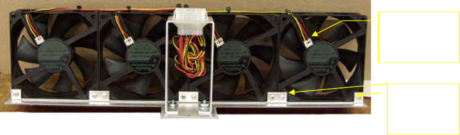
MXi HALF PALLET OPERATIONS AND MAINTENANCE
PUB07-03 Rev 1 July 17, 2007 07-03-11 MXi Half Pallet Operations and Maintenance
6.2 REPLACING THE ENTIRE FAN ARRAY
In the event of a fan failure, LARCAN recommends replacing the entire array, as all fans have a similar lifespan.
1. Remove the fan array as described in Section 6.1.
2. Slide the new fan array into the MXi. The power connection is aligned so that it connects when the
mounting plate is fully in place.
3. Insert and tighten the five mounting screws. Note: Screws only need to be snug; do not overtighten.
6.3 REPLACING A SINGLE FAN
1. Remove the fan array as described in Section 6.1.
2. Each of the four fans is attached to the mounting plate via two screw-and-nut assemblies. Remove the
screws and nuts and set aside.
Figure 14 Fan Attachment to Mounting Plate
3. Disconnect the three-pin wiring harness connection by gently sliding it back with a fingernail or small
plastic tool.
4. If necessary, carefully cut and remove the zip tie holding the wires to the fan frame.
5. Remove the defective fan and replace with a known good fan of exactly the same dimensions and
specifications.
6. Re-connect the three-pin wiring harness connection.
7. Re-fasten the two screw-and-nut assemblies holding the fan to the mounting plate.
8. If necessary, replace the zip tie holding the wires to the fan frame.
9. Replace fan array into MXi as described in Section 6.1.
Screw-and-
nut
assemblies
Three-pin
wiring harness
connector
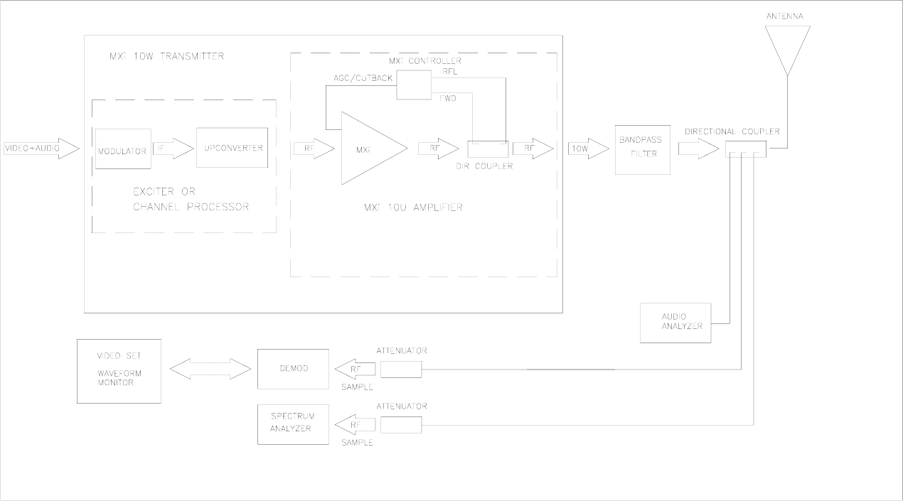
MXi HALF PALLET OPERATIONS AND MAINTENANCE
PUB07-03 Rev 1 July 17, 2007 07-03-12 MXi Half Pallet Operations and Maintenance
7 TEST EQUIPMENT SETUP
Figure 15 Test Equipment Setup
MXi HALF PALLET OPERATIONS AND MAINTENANCE
PUB07-03 Rev 1 July 17, 2007 07-03-13 MXi Half Pallet Operations and Maintenance
8 SPECIFICATIONS
Specifications are subject to change without notice.
8.1 ELECTRICAL
AC Line Input .....................................................................................................................90 to 264VAC, 50 to 60Hz
Power Consumption ............................................................................................................................ 260VA (typical)
8.2 ENVIRONMENTAL
Ambient Temperature .....................................................................................................0°C to +45°C (0°F to 113°F)
Humidity ..................................................................................................................................................... 0% to 90%
Altitude ..............................................................................................................................................2286 m (7500 ft)
8.3 COOLING
Four 4” muffin fans push air through the heatsink, and through the rear panel perforations.
8.4 DIMENSIONS
The Amplifier and Channel Processor chassis are standard 19" rack wide units.
Height
Amplifier........................................................................................................................................5.25" (3RU)
Exciter or Channel Processor.......................................................................................................1.75” (1RU)
Total Height ..................................................................................................................................7.00” (4RU)
Depth is 25" including a 3" allowance for connectors.
8.5 SHIPPING WEIGHT
Weight ……………………………….……… ......................................................................Approximately 14kg (31lbs)
MXi HALF PALLET AMPLIFIER CHASSIS
PUB07-04 Rev 1 July 18, 2007 07-04-i MXi Half Pallet Amplifier Chassis
CONTENTS
1 MXi HALF PALLET AMPLIFIER.................................................................................................................................1
FIGURES
FIGURE 1 FRONT VIEW OF MXI AMPLIFIER..................................................................................................................................1
FIGURE 2 REAR VIEW OF MXI AMPLIFIER....................................................................................................................................1
FIGURE 3 MXI FAN ARRAY ..........................................................................................................................................................2
FIGURE 4 MXI INTERIOR ..............................................................................................................................................................2
FIGURE 5 41D2047A MXI ASSEMBLY DIAGRAM SHT1 REV 0......................................................................................................3
FIGURE 6 41D2085 MXI SCHEMATIC SHT1 REV 0........................................................................................................................4
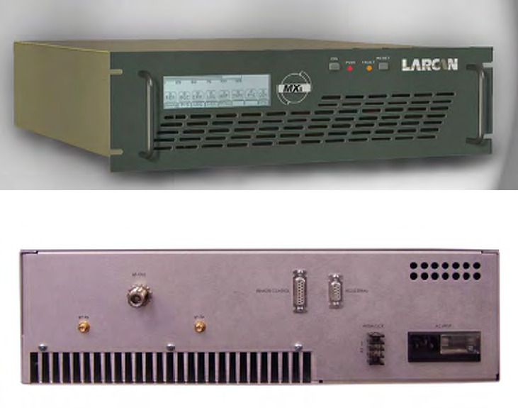
MXi HALF PALLET AMPLIFIER CHASSIS
PUB07-04 Rev 1 July 18, 2007 07-04-1 MXi Half Pallet Amplifier Chassis
1 MXi HALF PALLET AMPLIFIER
The MXi Amplifier Chassis Assembly 41D2047G2 consists of a standard 19" rack mountable 5.25" (3RU)
enclosure containing the amplifier heatsink assembly, a fan array assembly consisting of four DC cooling fans, a
controller board with built-in RF detectors, and a front panel consisting of ON/OFF, RESET switches and an
LCD/Touchpad, and a rear panel assembly with connectors for interfacing to external equipment. A dual output
DC power supply for powering the amplifier, the controller and the cooling fans is also housed in this enclosure.
Figure 1 is a front view of the MXi amplifier, showing the LCD Touchpad display, ON/OFF switch, Status PWR
(Green) and FAULT (Red) LEDs, and RESET switch.
Figure 1 Front View of MXi Amplifier
Figure 2 Rear View of MXi Amplifier
The rear of the MXi AMPLIFIER has the following connectors (from left to right):
• RF IN SMA connector-
• RF OUT N connector
• RF TP SMA connector – RF sample
• REMOTE CONTROL 15-pin D-shell connector
• RS232 SERIAL nine-pin connector
• INTERLOCK terminal board
• AC INPUT
The MXi is classified as a broadband amplifier, thus it is operational to cover the entire UHF television spectrum
ranging in frequencies from 470MHz to 860MHz.
Controlled DC power to the amplifier assembly comes from the high efficiency 500W switching power supply via a
two-pin connector, J4 of the MXi Controller Board. Regulated DC of +32V from the switching power supply is the
B+ voltage to the amplifier heatsink assembly. The second auxiliary output of the power supply is +12VDC, which
is used for powering the controller and the cooling fans.
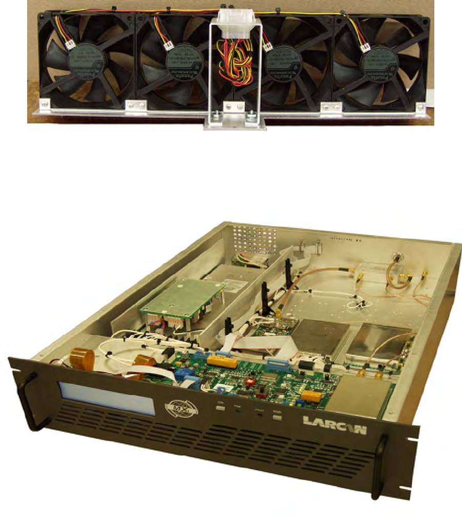
MXi HALF PALLET AMPLIFIER CHASSIS
PUB07-04 Rev 1 July 18, 2007 07-04-2 MXi Half Pallet Amplifier Chassis
The heatsink cooling fans are the +12DC, 4" muffin model. Typically, they come ON at the same time B+ is
applied to the power amplifier. It is connected to the controller PC board connector, J8. As built, the cooling fans
push air from the front panel through the heatsink and through the perforations in the rear panel. This assembly is
located underneath the MXi Controller board.
Figure 3 MXi Fan Array
A thermal switch is mounted on the heatsink where the operating temperature is sensed. If this temperature
increases beyond the trip point of the thermal switch, which is about 60°C, its contact opens and breaks the
interlocking circuit of the MXi amplifier. The interlock circuit ultimately controls the power supply to the power
amplifier and therefore shuts down and remains OFF until the heatsink cools down to about 50°C.
Figure 4 MXi Interior
A directional coupler is also mounted on the heatsink and provides forward and reflected RF signals to the
controller. These RF samples are detected and processed on the MXi controller to provide DC outputs
corresponding to these signals. They are then used for AGC, VSWR supervision and also for providing digital
metering available on the front panel LCD touchpad.
The MXi amplifier assembly diagram is shown in Figure 5.
The chassis is wired according to the functional diagram 41D2085 as shown in Figure 6.
MXi 500W POWER SUPPLY
PUB05-67 Rev 1 July 17, 2007 05-67-i MXi 500W Power Supply
CONTENTS
1 MXi 500W POWER SUPPLY LAR500-32-P5337..........................................................................................................1
2 POWER SUPPLY MANUAL REPRINT........................................................................................................................3
FIGURES
FIGURE 1 MXI 500W POWER SUPPLY ..........................................................................................................................................1
FIGURE 2 12-TERMINAL INTERFACE BOARD ................................................................................................................................1
FIGURE 3 41D2047A MXI HOUSING ASSEMBLY SHT1 REV 0.......................................................................................................7
FIGURE 4 41D1065 MXI WIRING DIAGRAM SHT1 REV 0 .............................................................................................................8
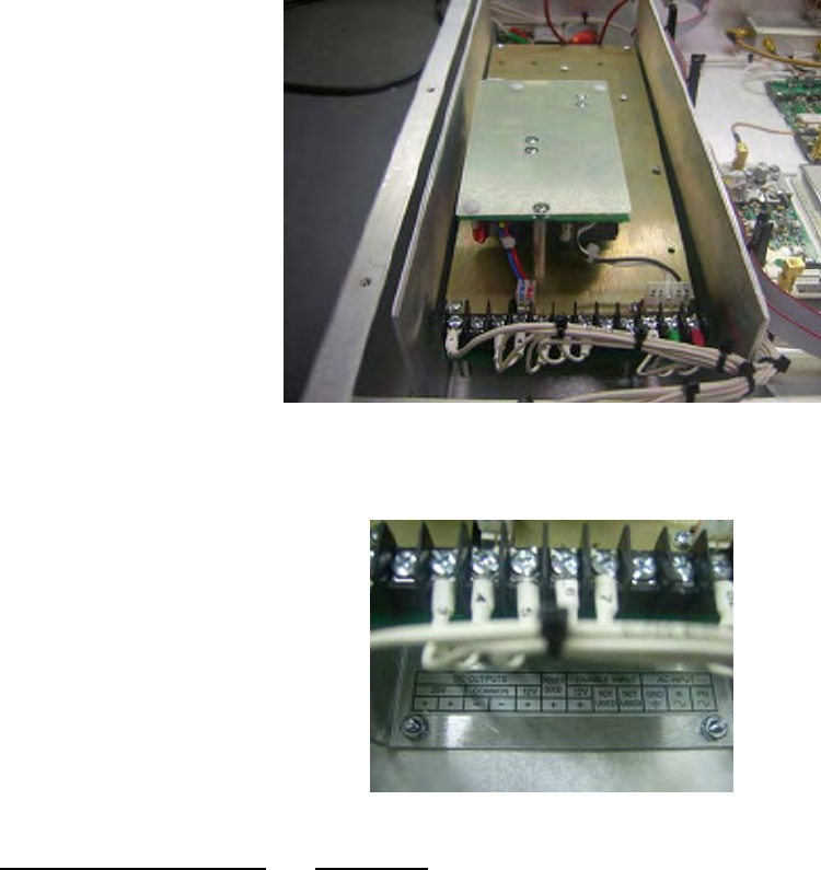
MXi 500W POWER SUPPLY
PUB05-67 Rev 1 July 17, 2007 05-67-1 MXi 500W Power Supply
1 MXi 500W POWER SUPPLY LAR500-32-P5337
The LAR500-32-P337 power supply used in the MXi single pallet amplifier is a free-standing, power factor
corrected 500W unit. It has the capability to deliver up to 15 Amps when the power supply output is set to
+32VDC. The design of this unit results in a highly efficient power supply ideal for the MXi power level. This unit
also contains an internal auxiliary 12VDC power supply rated at 3 Amps which is used to provide power to the
MXi Controller board as well as supplying power to the cooling fans. This auxiliary power supply provides
+12VDC output as long as the main AC input is present. Refer to wiring and functional diagram 41D2085, Figure
4, for detailed wiring information.
Figure 1 MXi 500W Power Supply
A 12-terminal interface board is used in the power supply for interfacing to various sub-assemblies in the MXi
enclosure. The following describes the function of each terminal.
Figure 2 12-Terminal Interface Board
TERMINAL/DESCRIPTION FUNCTION
1. +32VDC OUTPUT First of two +32VDC outputs of the power supply
2. +32VDC OUTPUT Second of two +32VDC outputs of the power supply
3. COMMON (–) return of the 32V and 12V power supply
4. COMMON (–) return of the 32V and 12V power supply
5. +12VDC OUTPUT +12VDC for powering the MXi controller
6. POWER GOOD A High (+12V) is measured here if the +28V power supply is OK
7. +12V ENABLE INPUT If +12V is applied here, it will turn ON the +28VDC power supply.
This enable signal comes from the MXi controller board provided the interlocks
are closed and there are no fault conditions.
MXi 500W POWER SUPPLY
PUB05-67 Rev 1 July 17, 2007 05-67-2 MXi 500W Power Supply
8. NOT USED
9. NOT USED
10. GND AC GND
11. N AC Neutral
12. PH AC Phase (Line)
MXi 500W POWER SUPPLY
PUB05-67 Rev 1 July 17, 2007 05-67-3 MXi 500W Power Supply
2 POWER SUPPLY MANUAL REPRINT
The following pages are a reprint of the operating manual of LAR500-32-P337 switching power supply, with
permission from Absopulse Electronics Ltd.
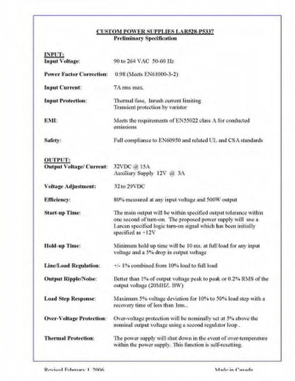
MXi 500W POWER SUPPLY
PUB05-67 Rev 1 July 17, 2007 05-67-4 MXi 500W Power Supply
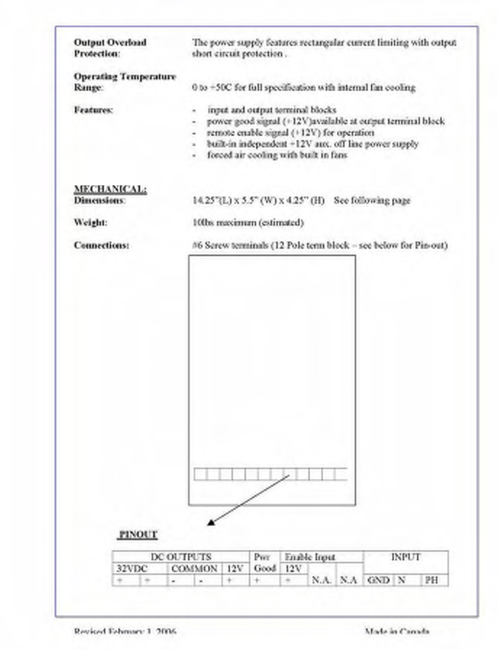
MXi 500W POWER SUPPLY
PUB05-67 Rev 1 July 17, 2007 05-67-5 MXi 500W Power Supply
MXi 500W POWER SUPPLY
PUB05-67 Rev 1 July 17, 2007 05-67-6 MXi 500W Power Supply
MXi AMPLIFIER CONTROLLER BOARD REV.2
PUB06-82 Rev. 1 July 17, 2007 06-82-i MXi Amplifier Controller Board Rev.2
CONTENTS
1 INTRODUCTION .............................................................................................................................................................1
2 GENERAL OPERATIONS ..............................................................................................................................................3
2.1 CONNECTOR AND SIGNAL DEFINITIONS........................................................................................................................3
2.1.1 J1 BDM (Background Debug Mode) Connection................................................................................................3
2.1.2 J2 Remote RS232 Connection..............................................................................................................................3
2.1.3 J3 Front Panel LCD and Touchpad.....................................................................................................................3
2.1.4 J4 +32 Volt DC Power Supply.............................................................................................................................3
2.1.5 J5 +32 Volt DC Power Supply Sensing (External)..............................................................................................3
2.1.6 J6 Remote Controls..............................................................................................................................................3
2.1.7 J7 Transmitter Switch Interface...........................................................................................................................4
2.1.8 J8 Fan Interface...................................................................................................................................................4
2.1.9 J9 External Controls............................................................................................................................................4
2.1.10 J10 AGC Control .................................................................................................................................................4
2.1.11 J11 Aural Detector (Optional).............................................................................................................................4
2.1.12 J12 Forward RF Sample......................................................................................................................................4
2.1.13 J13 Reflected RF Sample .....................................................................................................................................4
2.1.14 J14 Front Panel LCD Power ...............................................................................................................................4
2.2 JUMPER OPTIONS..........................................................................................................................................................4
2.2.1 BDM Slide Switch S2 ...........................................................................................................................................4
2.3 FRONT PANEL AND CONTROL INDICATORS...................................................................................................................7
2.3.1 Default/Normal E5= Ext E7=Out........................................................................................................................7
2.3.2 Manual Override E5= Int E7=Out......................................................................................................................7
2.3.3 Remote Override E5= Ext E7=In ........................................................................................................................7
2.3.4 Manual and Remote Override E5= Int E7=In.....................................................................................................7
2.4 RF DETECTOR OPERATION ...........................................................................................................................................8
2.5 AGC, VSWR AND CUTBACK OPERATION ....................................................................................................................9
2.6 INTERLOCKS ...............................................................................................................................................................10
2.6.1 Hard Interlocks..................................................................................................................................................10
2.6.2 Soft Interlocks ....................................................................................................................................................11
2.7 EXTERNAL SIGNALS AND REMOTE CONTROL.............................................................................................................11
2.7.1 External #1 Interlock .........................................................................................................................................11
2.7.2 Remote Controls (Individual).............................................................................................................................12
2.7.3 Remote Interface (Serial)...................................................................................................................................12
2.7.4 Transmitter Switching Interface.........................................................................................................................12
2.7.5 External DC Power Supply................................................................................................................................12
3 LCD GUI INTERFACE AND TOUCHPAD.................................................................................................................13
3.1 MAIN SCREEN AND TOUCHPAD OPERATIONS .............................................................................................................13
3.1.1 REM...................................................................................................................................................................14
3.1.2 AGC ...................................................................................................................................................................14
3.1.3 ERR....................................................................................................................................................................14
3.1.4 LOG ...................................................................................................................................................................14
3.1.5 AMP...................................................................................................................................................................15
3.1.6 P/S......................................................................................................................................................................15
3.1.7 INTK ..................................................................................................................................................................15
3.1.8 GEN ...................................................................................................................................................................15
3.2 AMPLIFIER SCREEN ....................................................................................................................................................15
3.2.1 TRIP...................................................................................................................................................................17
3.2.2 L/O.....................................................................................................................................................................17
3.2.3 RF ......................................................................................................................................................................17
3.2.4 INTK ..................................................................................................................................................................17
3.2.5 PSOK .................................................................................................................................................................17
3.2.6 FAN1..................................................................................................................................................................17
MXi AMPLIFIER CONTROLLER BOARD REV.2
PUB06-82 Rev. 1 July 17, 2007 06-82-ii MXi Amplifier Controller Board Rev.2
3.2.7 FAN2..................................................................................................................................................................18
3.2.8 FAN3..................................................................................................................................................................18
3.3 POWER SUPPLY SCREEN .............................................................................................................................................18
3.3.1 OK STAT............................................................................................................................................................19
3.3.2 PS ON ................................................................................................................................................................19
3.3.3 INTK ..................................................................................................................................................................19
3.3.4 FAN....................................................................................................................................................................19
3.4 INTERLOCKS SCREEN..................................................................................................................................................19
3.4.1 TRIP...................................................................................................................................................................20
3.4.2 L/O.....................................................................................................................................................................21
3.4.3 TEMP.................................................................................................................................................................21
3.4.4 PSOK .................................................................................................................................................................21
3.4.5 VOR....................................................................................................................................................................21
3.4.6 CUTB.................................................................................................................................................................21
3.4.7 FANS..................................................................................................................................................................21
3.5 REMOTE CONTROLS AND RS232 SERIAL SCREEN.......................................................................................................22
3.5.1 Remote ...............................................................................................................................................................23
3.5.2 NewFmt..............................................................................................................................................................23
3.5.3 ExtCmd ..............................................................................................................................................................23
3.5.4 SerCmd ..............................................................................................................................................................23
3.5.5 Error ..................................................................................................................................................................24
3.5.6 Logs Screen........................................................................................................................................................24
3.6 GENERAL SCREEN ......................................................................................................................................................25
4 SETUP PROCEDURES..................................................................................................................................................27
4.1 RF DETECTOR ............................................................................................................................................................27
4.2 AGC AND CUTBACK PROTECTION..............................................................................................................................29
4.2.1 AGC Setup..........................................................................................................................................................29
4.2.2 Cutback Setup ....................................................................................................................................................29
4.3 VSWR PROTECTION...................................................................................................................................................29
4.4 REMOTE CONTROL INTERFACE BAUD ........................................................................................................................30
4.5 POWER SUPPLY VOLTAGE AND CURRENT CALIBRATION............................................................................................31
5 REMOTE CONTROL CONNECTIONS MXi TRANSMITTER...............................................................................32
5.1 REMOTE CONTROLS....................................................................................................................................................32
5.1.1 RC_TX_On Remote Transmitter ON Control ....................................................................................................33
5.1.2 RC_TX_Off Remote Transmitter OFF Control..................................................................................................33
5.1.3 RC_TX_VOR Remote Transmitter VOR Control ...............................................................................................34
5.1.4 RC_RESET Remote RESET Control..................................................................................................................34
5.2 EXT1 SECONDARY EXTERNAL #1 INTERLOCK ...........................................................................................................34
5.2.1 Status Outputs....................................................................................................................................................35
5.3 TELEMETRY OUTPUTS ................................................................................................................................................35
6 CIRCUIT DESCRIPTIONS...........................................................................................................................................37
6.1 MC68HC908 MICROPROCESSOR................................................................................................................................37
6.2 POWER SUPPLY VOLTAGE AND CURRENT MONITORING ............................................................................................38
6.3 ON/OFF RELAY K1....................................................................................................................................................40
6.4 AGC, CUTBACK AND VSWR....................................................................................................................................40
6.5 SPI UART..................................................................................................................................................................41
6.6 SPI NVPOT ...............................................................................................................................................................42
6.7 RF DETECTOR ............................................................................................................................................................42
6.7.1 Circuit Description ............................................................................................................................................42
6.8 J12 CHANNEL – VISUAL FORWARD ............................................................................................................................42
6.9 J13 CHANNEL – REFLECTED .......................................................................................................................................43
6.10 J12 CHANNEL – AURAL FORWARD .............................................................................................................................44
7 ADDENDUMS .................................................................................................................................................................45
MXi AMPLIFIER CONTROLLER BOARD REV.2
PUB06-82 Rev. 1 July 17, 2007 06-82-iii MXi Amplifier Controller Board Rev.2
7.1 ADDENDUM 1– CDS51405 DISPLAY CONTROLLER....................................................................................................46
7.2 ADDENDUM 2–DUAL DIGITAL POTENTIOMETER WITH EEPROM .............................................................................49
7.3 ADDENDUM 3–SPI/MICROWIRE-COMPATIBLE UART AND +/-15KV ESD-PROTECTED RS-232 TRANSCEIVERS
WITH INTERNAL CAPACITORS.................................................................................................................................................52
7.4 ADDENDUM 4–MC68HC908GTXX DATA SHEET .....................................................................................................55
7.5 ADDENDUM 5– CURRENT TRANSDUCER HXS 20-NP.................................................................................................62
FIGURES
FIGURE 1 MXI CONTROLLER........................................................................................................................................................1
FIGURE 2 MXI FRONT PANEL .......................................................................................................................................................1
FIGURE 3 MAIN MENU SCREEN ....................................................................................................................................................2
FIGURE 4 AMPLIFIER (AMP) SUBMENU .......................................................................................................................................2
FIGURE 5 POWER SUPPLY (P/S) SUBMENU SCREEN......................................................................................................................2
FIGURE 6 AMPS SUBMENU SCREEN ..............................................................................................................................................9
FIGURE 7 SAMPLE POWER-UP SCREEN.......................................................................................................................................13
FIGURE 8 MAIN MENU SCREEN ..................................................................................................................................................13
FIGURE 9 AMPS SUBMENU..........................................................................................................................................................16
FIGURE 10 POWER SUPPLY SUBMENU SCREEN...........................................................................................................................18
FIGURE 11 TRANSMITTER ON, INTERLOCKS OK SCREEN ...........................................................................................................20
FIGURE 12 TRANSMITTER ON, INTERLOCKS BAD SCREEN..........................................................................................................20
FIGURE 13 TRANSMITTER OFF, INTERLOCKS OK SCREEN ..........................................................................................................20
FIGURE 14 REMOTE CONTROL SUBMENU...................................................................................................................................22
FIGURE 15 LOGS SUBMENU SCREEN...........................................................................................................................................25
FIGURE 16 GENERAL SUBMENU SCREEN ....................................................................................................................................26
FIGURE 17 AMPS SUBMENU SCREEN ..........................................................................................................................................29
FIGURE 18 REMOTE CONTROL SUBMENU SCREEN......................................................................................................................30
FIGURE 19 POWER SUPPLY SUBMENU SCREEN...........................................................................................................................31
FIGURE 20 TX_OFF, RESET, AND VOR REMOTE CONTROLS...................................................................................................32
FIGURE 21 TX_ON REMOTE CONTROL......................................................................................................................................32
FIGURE 22 STATUS OUTPUTS......................................................................................................................................................35
FIGURE 23 MXI CONTROLLER BOARD ASSEMBLY DIAGRAM 31C1897A2 SHT1 REV 2.2 ..........................................................65
FIGURE 24 MXI CONTROLLER BOARD SCHEMATIC 31C1897S1 SHT1 REV 2.3..........................................................................66
FIGURE 25 MXI CONTROLLER BOARD SCHEMATIC 31C1897S2 SHT2 REV 2.3..........................................................................67
FIGURE 26 MXI CONTROLLER BOARD SCHEMATIC 31C1897S3 SHT3 REV 2.3..........................................................................68
FIGURE 27 MXI CONTROLLER BOARD SCHEMATIC 31C1897S4 SHT4 REV 2.3..........................................................................69
FIGURE 28 MXI CONTROLLER BOARD SCHEMATIC 31C1897S5 SHT5 REV 2.3..........................................................................70
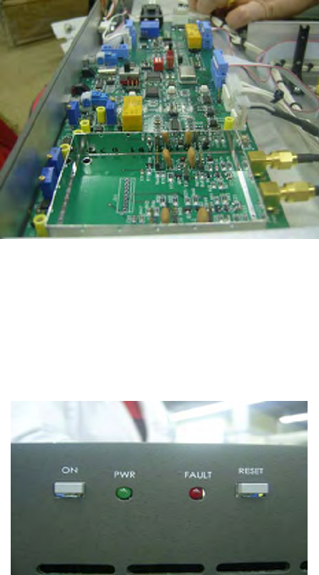
MXi AMPLIFIER CONTROLLER BOARD REV.2
PUB06-82 Rev 1 July 17, 2007 06-82-1 MXi Amplifier Controller Board Rev.2
1 INTRODUCTION
This manual describes revision 2.0 or higher of the circuit board.
The MXi control board (Assembly 31C1897) is a single-circuit assembly that provides all of the control functions
required for the MXi series of transmitters on a single circuit board. This board can be configured for a number of
different transmitter types, power levels, transmission standards and options.
Figure 1 MXi Controller
The MXi control board provides local front panel interface via ON/OFF and RESET buttons as well as a graphical
user interface through a front panel LCD assembly with touchpad for user commands. The board implements
controls/status/telemetries for remote control through a rear panel connector that will interface to a typical remote
control system (such as Moseley or Gentner). An RS232 serial port is also provided to allow the operator to
access the MXi through an external computer (with the appropriate software). The MXi control board has RF
detectors for forward and reflected power and all the circuitry to support AGC/VSWR/Cutback functions. Circuitry
to control and monitor the +32V power supply is also included on this board.
Figure 2 MXi Front Panel
The user interface to the amplifier is accomplished with the front panel LCD that incorporates a touchpad as an
integral part of the unit. The LCD has the capability of displaying a variety of screens, which are selected by the
user via the touchpad. Figure 3 shows the LCD main menu, which shows the present status of the amplifier along
with the selections of submenus.
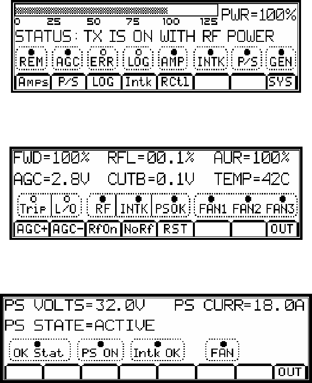
MXi AMPLIFIER CONTROLLER BOARD REV.2
PUB06-82 Rev 1 July 17, 2007 06-82-2 MXi Amplifier Controller Board Rev.2
Figure 3 Main Menu Screen
Forward (FWD) and Reflected power (RFL), AURal power, AGC and CUTBack (VSWR) control voltage, as well
as the heatsink TEMPerature (Optional) can be displayed by selecting the AMP submenu as shown in Figure 4.
Figure 4 Amplifier (AMP) Submenu
Pressing the power supply P/S submenu from the Main Menu will display the power supply voltage and current
consumption as well as its status.
Figure 5 Power Supply (P/S) Submenu Screen
The MXi board has a BDM (Background Debug Mode) connector that allows an external computer or laptop to
download the software program into the CPU chip. The CPU chip holds the program in its internal Flash memory
and so there is no external chip or device that need be replaced to change/upgrade the software.
The concept of this design places all of the control and monitoring functions in one place and therefore eases the
setup and maintenance functions on this series of transmitters.
MXi AMPLIFIER CONTROLLER BOARD REV.2
PUB06-82 Rev 1 July 17, 2007 06-82-3 MXi Amplifier Controller Board Rev.2
2 GENERAL OPERATIONS
2.1 CONNECTOR AND SIGNAL DEFINITIONS
The connectors on the MXi control board are all shown in Figure 26, which is sheet #3 of the Schematic. The
individual signals that are associated with each pin of the connector are also given. A brief description of each of
the connectors on the board follows.
2.1.1 J1 BDM (Background Debug Mode) Connection
This is used by the software developer to debug the software programmed into the HC08 CPU.
The software program is also downloaded into the HC08 CPU via this connector.
The operator has no real use for this connector since it requires a special interface board.
2.1.2 J2 Remote RS232 Connection
This connector would normally have a nine-pin ribbon cable attached to route the serial signals to the rear panel
nine-pin D-shell connector. Although J2 has 10 pins, only the first nine are actually used with pin 10 being left
open. A typical three-wire serial port (TxD, RxD and Ground) is implemented on this connector to allow interface
to an external laptop or PC.
2.1.3 J3 Front Panel LCD and Touchpad
This uses a nine-wire ribbon cable to send and receive serial data from the Front Panel LCD/Touchpad assembly.
Although J3 has 10 pins, only the first nine are actually used with pin 10 being left open. This connection is a
typical three-wire serial port (TxD, RxD and Ground) that communicates with the LCD/Touchpad.
2.1.4 J4 +32 Volt DC Power Supply
This is a two-pin connector used for the +32VDC power that is supplied to the RF amplifier. The +32V source is
fed into one pin, run through a current sensor on the MXi board and then fed back out the second pin to the RF
Amplifier. This is the manner in which the current that the +32V power supply is measured. The voltage telemetry
sample from the +32V power is also taken from this connector. When an internal power supply without its own
current metering is being used, this connector is functional. If an external power supply with its own current
metering is being utilized, this connector is left open.
2.1.5 J5 +32 Volt DC Power Supply Sensing (External)
This uses a six-pin connector that has all the interface connections for the +32V power supply. Included is an ON
command, P/S OK status and a ground reference from the power supply. In the case where an external power
supply is being used with its own current metering, the +32V sample and the current telemetry is fed into this
connector.
The last signal on this connector is a +12V power supply input (either from the +32V power supply or an external
+12V power supply) that is used to power the MXi controller board itself. The ground reference is shared with that
of the +32V power supply.
2.1.6 J6 Remote Controls
This uses a 15-wire ribbon cable to send status/telemetry and receive commands from the rear panel 15-pin D-
shell connector. Although J6 has 16 pins, only the first nine are actually used with pin 16 being left open. In
addition to the remote signals, there is a single set of contacts made available as an external interlock. This can
connect to an external device or be used as a simple remote ON/OFF.
MXi AMPLIFIER CONTROLLER BOARD REV.2
PUB06-82 Rev 1 July 17, 2007 06-82-4 MXi Amplifier Controller Board Rev.2
2.1.7 J7 Transmitter Switch Interface
This uses a nine-wire ribbon cable to send status/telemetry and receive commands from the rear panel nine-pin
D-shell connector. Although J7 has 10 pins, only the first nine are actually used with pin 10 being left open. This
ribbon cable may not be installed if there is only a single transmitter system or if there is no transmitter switching
unit included in the RF system.
2.1.8 J8 Fan Interface
This uses a special connector mounted on the bottom of the MXi controller board to connect to the fan assembly.
The fan assembly normally includes up to four fans that are mounted below the MXi controller board and is
inserted from the bottom of the transmitter control chassis. This connector has ON/POWER control for each of the
fans along with a ground reference and a rotational status signal that comes from each of the fans.
2.1.9 J9 External Controls
This has a seven-pin connector that is used to input a variety of signals into the MXi controller. A pair of pins are
used for the External interlock that is connected to a terminal block on the rear chassis (this is in parallel with the
external interlock on the Remote Controls J6). There is also a thermal interlock that is sent from the RF amplifier.
Provision has been made for a thermistor input to measure temperatures for testing purposes. A remote control
VOR (Video Operated Relay) input (RC_VOR) is made available which is in parallel with the RC_VOR control
input of the Remote Controls J6.
2.1.10 J10 AGC Control
This is a three-pin connector that sends a DC reference voltage (with ground reference and shield) to the RF
preamplifier module. This DC reference is generated by the AGC circuitry on the MXi Controller to control the RF
output level of the amplifier.
2.1.11 J11 Aural Detector (Optional)
This is an 11-pin connector that allows the option aural RF detector to be mounted above the normal RF
detectors. This connector is located in the shielded box on the left side of the MXi Controller board and is not
normally visible if the cover is installed on the shield box.
2.1.12 J12 Forward RF Sample
This SMA connector receives the forward power sample from the directional coupler that is mounted on the RF
amplifier heatsink. This is used by the RF detector to monitor the level of the RF forward power.
2.1.13 J13 Reflected RF Sample
This SMA connector receives the reflected power sample from the directional coupler that is mounted on the RF
amplifier heatsink. This is used by the RF detector to monitor the level of the RF reflected power.
2.1.14 J14 Front Panel LCD Power
This is a two-pin connector that sends power (+5V and ground) to the Front Panel LCD/Touchpad assembly.
2.2 JUMPER OPTIONS
2.2.1 BDM Slide Switch S2
2.2.1.1. Dip Switch S3 System Configuration
These DIP switches are reserved for factory test and system configuration. At the time of publication, they are not
assigned for specific functions.
MXi AMPLIFIER CONTROLLER BOARD REV.2
PUB06-82 Rev 1 July 17, 2007 06-82-5 MXi Amplifier Controller Board Rev.2
2.2.1.2. Jumper E1–Debug/Normal Mode
This jumper allows factory programming and debug of the HC08 microcontroller. This should always be in the
Normal position for proper operation in the field.
2.2.1.3. Jumper E2–Remote Control Reset
This jumper allows the operator to use the remote Reset command to effect a reset of the HC08 microcontroller.
This would only be installed if there were a suspicion that the microprocessor is hanging-up and the operator
would intend to reset it remotely. This is purely for diagnostic purposes only and should not normally be
permanently installed.
2.2.1.4. Jumper E3–Spare Line Configuration
This jumper allows the signal into the PA0 pin 32 of the HC08 microcontroller to be configured as either an input
or output. This configuration would already have been done in the software at the factory and this jumper setting
should not be altered in the field unless directed by LARCAN personnel.
2.2.1.5. Jumper E4–External or Internal Power Supply Current Sensing
The MXi Amplifier can be configured with a +32VDC power supply that has a built-in current sensing telemetry or,
when the power supply lacks this facility, the MXi controller can measure the current from the +32VDC supply
using the onboard current sensor. When the power supply has its own current sensing telemetry, jumper E4
would be set to the External position. When the power supply does not have its own current sensing telemetry,
jumper E4 would be set to the Internal position allowing the controller’s own current sensor to provide the
telemetry. This jumper is normally set at the factory and should not be altered in the field.
2.2.1.6. Jumper E5–Front Panel ON/OFF Control Switch (System/Manual)
This jumper controls the function of the front panel ON/OFF switch. When in the Ext position, the ON/OFF
command is fed through the HC08 microcontroller allowing the operator to utilize remote ON and OFF
commands. When in the Int position, the ON/OFF directly controls the ON/OFF relay bypassing the
microcontroller and disabling its OFF control ability.
2.2.1.7. Jumper E6–Tx Switching Interlock Enable
Facility has been designed into the controller interlock chain to allow an external interlock contact that a
transmitter switching unit could use to force the amplifier into an OFF state. This would occur if the controller is
moving a coax switch or if this amplifier has been removed from the antenna. When there is no transmitter
switching unit installed, jumper E6 would be installed to disable this particular interlock.
2.2.1.8. Jumper E7–Manual Remote ON/OFF Control
This jumper would be installed to allow the operator to manually turn the amplifier ON or OFF via a remote
command that would directly control the ON/OFF relay and bypass the HC08 microcontroller. For this mode to
work properly, the front panel ON/OFF switch should be left in the OFF position. In normal operation, this jumper
is not installed.
2.2.1.9. Jumper E8–Forward RF Detector, Peak or Average Power
This jumper selects whether the intermediate stage of the RF detector of the Forward power will measure Peak or
Average power. When measuring digital signals, the jumper would normally be set to Average and when
measuring analog signals the jumper would be set to Peak. This jumper determines the amount of RC filtering (or
averaging) of the signal power by selecting which value of resistance is placed in series with capacitor C22. This
jumper is set by the factory depending on the signal standard of the particular amplifier and level that is obtained
from the RF coupler. This should not be changed in the field.
MXi AMPLIFIER CONTROLLER BOARD REV.2
PUB06-82 Rev 1 July 17, 2007 06-82-6 MXi Amplifier Controller Board Rev.2
2.2.1.10. Jumper E9–Forward RF Detector Color Burst Trap
When installed, this jumper enables the filter that removes the color burst from the RF signal. This would only be
installed on the analog transmitters, as the digital amplifier does not have a color burst.
2.2.1.11. Jumper E10–Forward RF Detector Sound Carrier Trap
When installed, this jumper enables the filter that removes the sound carrier from the RF signal. This would only
be installed on the analog transmitters, as the digital amplifier does not have a sound carrier.
2.2.1.12. Jumper E11–Forward RF Detector Final Gain Control
This jumper selects either a high or low gain for the final stage of the RF detector of the Forward power. This
jumper is set by the factory depending on the output power of the particular amplifier and level that is obtained
from the RF coupler. This should not be changed in the field.
2.2.1.13. Jumper E12–Reflected RF Detector, Peak or Average Power
This jumper selects whether the intermediate stage of the RF detector of the Reflected power will measure Peak
or Average power. When measuring digital signals, the jumper would normally be set to Average and when
measuring analog signals the jumper would be set to Peak. This jumper determines the amount of RC filtering (or
averaging) of the signal power by selecting which value of resistance is placed in series with capacitor C22. This
jumper is set by the factory depending on the signal standard of the particular amplifier and level that is obtained
from the RF coupler. This should not be changed in the field.
2.2.1.14. Jumper E13–Reflected RF Detector Color Burst Trap
When installed, this jumper enables the filter that removes the color burst from the RF signal. This would only be
installed on the analog transmitters, as the digital amplifier does not have a color burst.
2.2.1.15. Jumper E14–Reflected RF Detector Sound Carrier Trap
When installed, this jumper enables the filter that removes the sound carrier from the RF signal. This would only
be installed on the analog transmitters, as the digital amplifier does not have a sound carrier.
2.2.1.16. Jumper E15–Reflected RF Detector Final Gain Control
This jumper selects either a high or low gain for the final stage of the RF detector of the Reflected power. This
jumper is set by the factory depending on the output power of the particular amplifier and level that is obtained
from the RF coupler. This should not be changed in the field.
2.2.1.17. Jumper E16–AGC Disable Control
When installed, this jumper disables the AGC control of the transmitter and its controller. This is normally only
used with setting up the maximum input drive level for the amplifier. In normal operation, this jumper should
always be removed, since it can allow excessive power to be mistakenly fed through the amplifier.
2.2.1.18. Jumper E17–VSWR Disable Control
When installed, this jumper disables the VSWR trip interlock of the transmitter and its controller. This is normally
only to be used with setting up the VSWR trip level for the amplifier. In normal operation, this jumper should
always be removed, since it removes the VSWR protection from the amplifier. In the presence of a VSWR
condition, this could result in damage to the amplifier FET devices.
2.2.1.19. Jumper E18–Manual VSWR Reset Control
When installed, this jumper allows the operator to directly reset the VSWR trip relay and effectively bypass the
HC08 microcontroller. In normal operation, this jumper would not be installed.
MXi AMPLIFIER CONTROLLER BOARD REV.2
PUB06-82 Rev 1 July 17, 2007 06-82-7 MXi Amplifier Controller Board Rev.2
2.2.1.20. Jumper E19– Peak or Sync Detection
This jumper allows the forward power sample to be either a Peak detection or Back Porch detection using the
visual sync. The optional Aural detection piggyback board must be installed to provide the sync detection facility.
For most applications (including all of the digital modulation standards), jumper E19 would be set for peak (Pk)
since there is no vertical sync interval that can be locked onto for these signals. The only application where E19 is
set to the Sync position is when the optional Aural Detection board is installed and Back Porch detection for the
Forward power sample is desired. The purpose of using Back Porch detection is to regulate the output power
more precisely, independent of APL level. This jumper is set by the factory and should not be changed in the field.
2.3 FRONT PANEL AND CONTROL INDICATORS
The MXi has a very simple set of front panel controls and indications that consists of three primary sections.
The ON/OFF pushbutton can be set up to turn the transmitter ON or OFF for local control. This button is an
alternate action device that, once pressed, remains in the ON state (pressed in). If the operator presses the
button a second time, it releases into the OFF state. The function of this button can be set up for a variety of
operations depending on how the circuit board jumpers are configured. A brief description of the possible
configurations follows.
2.3.1 Default/Normal E5= Ext E7=Out
Allows the MXi CPU to directly control all local and remote ON/OFF commands. The front panel ON/OFF
command will only operate when the system is in local and the remote commands will only operate when the
system is in remote.
2.3.2 Manual Override E5= Int E7=Out
Forces the MXi circuitry to always respond to the front panel ON/OFF commands. The front panel ON/OFF
command is always active, so if it is left in the ON position, it will not be possible to shut OFF the transmitter
remotely with the ON/OFF command. However, a remote opening of the EXT1 interlock will shut down the
transmitter at all times. For proper remote operation in this condition, the operator must place the front panel
ON/OFF switch in the OFF position before leaving the site. This allows the remote command to operate normally.
2.3.3 Remote Override E5= Ext E7=In
Forces the MXi circuitry to always respond to the remote ON command. The transmitter remains ON as long as
the remote ON command is asserted. In this mode the remote command will always be active even if the system
has been placed in LOCAL mode. The front panel ON/OFF command will not be able to shut OFF the transmitter
while the remote ON/OFF command is asserted.
This is clearly an emergency type configuration and should not be used for normal operations. For proper front
panel operation in this condition, the operator must remove the remote ON/OFF command or disconnect the
remote connector to achieve local controls again.
2.3.4 Manual and Remote Override E5= Int E7=In
This enables the overrides on both the remote and local ON/OFF commands. The MXi circuitry will turn the
transmitter ON if either the Front Panel or the Remote ON command is present. These functions are independent
of the transmitters REMOTE or LOCAL mode. This is clearly an emergency type configuration and should not be
used for normal operations.
The green front panel LED (DS5 on the MXi board) beside the ON/OFF pushbutton indicates the current ON/OFF
state of the transmitter. This LED follows the condition of the ON/OFF relay K1 and is not affected by the source
of the ON/OFF command.
A second momentary front panel pushbutton is provided to reset any VSWR trips or lockout conditions. When a
VSWR Lockout has occurred, the transmitter is shut down. The operator must find the source of the VSWR and,
when repaired, this reset button will clear the lockout and the transmitter will automatically turn ON again. Note
MXi AMPLIFIER CONTROLLER BOARD REV.2
PUB06-82 Rev 1 July 17, 2007 06-82-8 MXi Amplifier Controller Board Rev.2
that a VSWR trip/Lockout does not change the ON/OFF state of the transmitter, it just opens an interlock to shut it
down.
The LED beside this pushbutton shows the state of the VSWR relay K2. When there is a VSWR trip, the MXi
controller resets it automatically until three trips occur in a one minute span. When a VSWR trip occurs, this LED
momentarily flashes, indicating that a trip did occur but the CPU has reset the trip. If three trips do occur that
result in a Lockout, this LED is on continuously and must be reset to clear it.
The MXi also provides a more detailed and graphical interface to the operator via the front panel LCD and
touchpad. This device has extensive information on the operations of the transmitter and provides a number of
controls to the transmitter. This device and its interface are described in Section 3.
2.4 RF DETECTOR OPERATION
The RF Detector circuitry is show in Figure 27. This circuitry can be used for internally diplexed analog
transmitters or for digital transmitters.
RF Power levels are sampled by a directional coupler located on the RF amplifier heatsink and the resulting RF
samples are detected and appropriately processed to provide DC outputs corresponding to the amplitude of the
desired parameter of the input signal. These DC outputs contribute to the AGC/VSWR supervision of the
transmitter and are also processed in analog to digital conversion circuits on the MXi controller board to provide
digital metering.
The RF Detector can have different group assemblies to support the NTSC system, the PAL system and Digital
transmission. NTSC and PAL application differ only in their color subcarrier frequency, consequently in a few
component values. All group assemblies use the same PC Board and have many jumpers used to change circuits
sensitivity, introduce/remove traps for color subcarrier and/or aural intercarrier and change envelope detector
characteristics for digital and analog applications.
The schematic included in this publication shows the circuitry for NTSC and Digital transmissions. For PAL
systems a separate schematic would be included that is currently not in this publication.
All jumpers are set in the factory and should not be modified in the field unless under direction from LARCAN
personnel.
An optional circuit board is available for internally diplexed analog systems to monitor the aural power separated
from the combined forward signal. This board is mounted on top of the existing RF detector circuitry in a piggy-
back configuration. This extra board uses a sync detector to obtain the back porch (blanking level) of the RF
signal and subtracts the overall RF signal level from the visual only signal level to obtain the aural output. When
this extra board is installed, an added benefit is the provision of a more stable visual output level that is more
independent of APL level due to the fact that the blanking level is used to determine power instead of a simple
envelope detection method. Note that the standard MXi transmitter does not come with this extra board installed
but it must be ordered as an option. When the option is included, an addendum to this manual will be included to
cover this option.
Required signal levels are as follows:
• FWD (overall forward sample) metering requires 20dBm sync peak signal for full scale (100% rated power).
• RFL (overall reflected sample) metering requires 10dBm sync peak signal for full scale (10% rated power).
The forward RF detector can be configured for a number of different signal types as the following table shows.
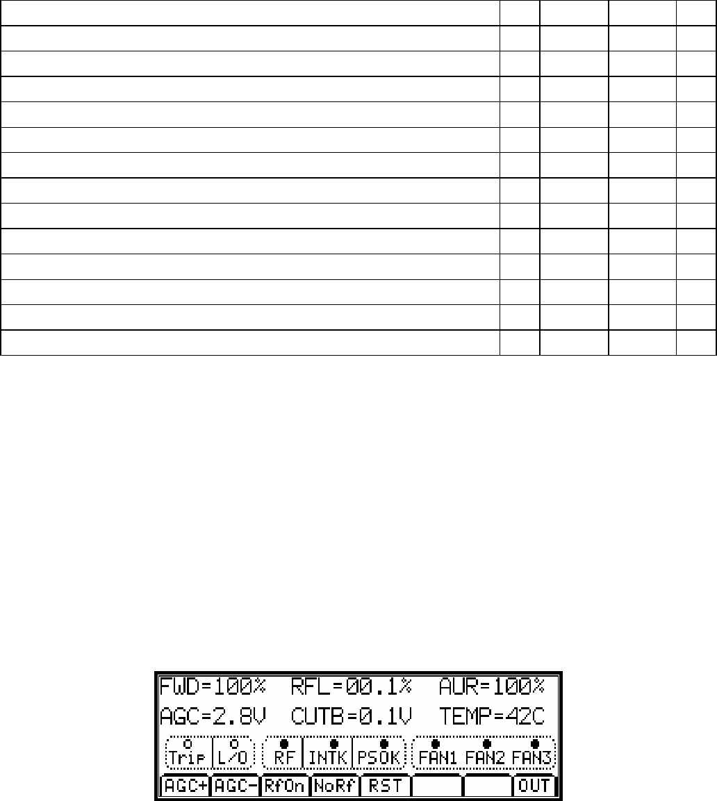
MXi AMPLIFIER CONTROLLER BOARD REV.2
PUB06-82 Rev 1 July 17, 2007 06-82-9 MXi Amplifier Controller Board Rev.2
DESCRIPTION E8 E9 E10 E11
Default Analog NTSC: +20dBm, Visual, Color Burst and Aur Carrier Trapped Pk Installed Installed LO
Default Analog NTSC: +20dBm, Visual, Color Burst and Aur Carrier Trapped Pk Installed Installed LO
Default Analog NTSC: +17dBm, Visual, Color Burst and Aur Carrier Trapped Pk Installed Installed HI
Default Analog NTSC: +17dBm, Visual, Color Burst and Aur Carrier Trapped Pk Installed Installed HI
Special Analog NTSC: +20dBm, Visual+Aural, Color Burst Trapped Pk Installed Absent LO
Special Analog NTSC: +20dBm, Visual+Aural, Color Burst Trapped Pk Installed Absent LO
Special Analog NTSC: +17dBm, Visual+Aural, Color Burst Trapped Pk Installed Absent HI
Special Analog NTSC: +17dBm, Visual+Aural, Color Burst Trapped Pk Installed Absent HI
Digital Signal: +20dBm, Ave Detector, No Traps (also Special Analog NTSC) Av Absent Absent LO
Digital Signal: +20dBm, Ave Detector, No Traps (also Special Analog NTSC) Av Absent Absent LO
Digital Signal: +17dBm, Ave Detector, No Traps (also Special Analog NTSC) Av Absent Absent HI
Digital Signal: +17dBm, Ave Detector, No Traps (also Special Analog NTSC) Av Absent Absent HI
Not Used: Visual + Color Burst and Aur Carrier Trapped X Absent Installed X
Two almost identical detector circuits reside on a single board for visual forward and reflected metering. Detection
sensitivity of the circuit dedicated to reflected visual power is approximately 10dB greater than for the visual
forward RF detector circuit. The reflected port reading is combined visual and aural power. The jumper
configuration for the reflected power follows that of the above table with E12 replacing E8; E13 replacing E9; E14
replacing E10; and E15 replacing E11.
2.5 AGC, VSWR AND CUTBACK OPERATION
The MXi board allows for an automatic gain control to maintain the transmitter’s power at a predefined level. The
operator must have first calibrated the RF detector to produce 4.0VDC at the desired 100% power level of the
transmitter. The exciter/modulator must then be set up to produce a drive level sufficient to allow 110% power
with no AGC controls applied. These operations are described in Section 4.
The AGC system generates a desired reference voltage that is set by the operator through the LCD touchpad. To
set the AGC, the operator calls up the Amps submenu from the Main LCD menu. He would then either press the
AGC+ button to increase the power level or the AGC– button to decrease the power level. This sets the reference
voltage for the AGC circuitry. If there is very low RF power, check that the RF status on the third line is lit. If it is
not, then the operator has shut down the RF. Pressing the RF ON menu button restores RF power. The Amps
submenu screen is shown below.
Figure 6 Amps Submenu Screen
The AGC circuit then compares this reference voltage to the actual voltage that is produced from the forward
power RF detector. If there is a difference, this is amplified by a high gain OpAmp and this error voltage is fed out
to connector J10. An external cable connects J10 to the attenuator on the RF preamp mounted on the heatsink.
This will lower the drive to the amplifiers until the transmitter power level agrees with the AGC reference voltage.
MXi AMPLIFIER CONTROLLER BOARD REV.2
PUB06-82 Rev 1 July 17, 2007 06-82-10 MXi Amplifier Controller Board Rev.2
Note the AGC voltage from the LCD, if it is near to a value of 0 (i.e., under 0.1V), then there is no AGC action left
and the power cannot be raised any further. If the amplifier power is under 100%, then check the RFL power level
and CUTBACK voltage to verify that the amplifier is not reducing power to protect from a VSWR condition.
The cutback circuit checks the level of reflected power as displayed on the LCD screen above [RFL=00.1%]. If
this reflected power is greater than 1%, the cutback circuit automatically reduces the amplifier forward power to
protect the devices. This indicates a mild VSWR condition such as may be caused by an icy antenna. The
cutback function is a safety protection and is therefore permanently in circuit and cannot (or should not) be
disabled. If the VSWR condition worsens such that reflected power exceeds 10% of forward power, the MXi shuts
the transmitter down.
The MXi has built-in VSWR protection to prevent damage to the amplifier from excessive power being reflected
back from the output system. This VSWR protection becomes operational when reflected power exceeds 10% of
forward power. The system shuts down the amplifier for a few seconds and then tries to restart again. This is
done to check if the VSWR was a temporary condition that could have been caused by a lightning strike nearby.
The LCD shows the TRIP status light on the third row of the LCD to indicate that a VSWR trip had occurred. If the
condition persists such that three VSWR trips occur within 1 minute, the system completely shuts down. The LCD
will then illuminate the L/O (Lockout) status light on the LCD to show that a Lockout has occurred.
2.6 INTERLOCKS
Interlocks on the MXi can be divided into two different types: hard interlocks that shut down the transmitter without
any CPU intervention and soft interlocks that are generated by the CPU chip in response to abnormal system
parameters.
2.6.1 Hard Interlocks
There are hardware interlocks that directly affect the ON/OFF relay K1 by removing the +12V arming voltage on
its coil and preventing it from turning on. There are four of these interlocks as follows:
2.6.1.1. Amplifier Thermal
Heatsink thermal opens if heatsink temperature is too high. Dry Contact across Connector J9 pins 5 and 6.
2.6.1.2. Transmitter Switching
Interlock provided for an external Transmitter Switching unit to shut down the Transmitter.
Dry Contact across Connector J7 pins 1 and 2.
When there is no transmitter switching, jumper E6 defeats this interlock.
2.6.1.3. External #1
Interlock supplied for customer use such as RF system interlock or RF Load.
Dry Contact across Connector J9 pins 1 and 2.
Parallel contact provided across J6 pins 14 and 15, only one of J6 or J9 is required.
If not used, then this contact should be shorted out externally.
2.6.1.4. VSWR Relay K2
Contact from VSWR Trip relay K2 pins 11 and 13.
Contact will be closed (OK) if there is no VSWR condition.
Contact will open whenever a VSWR is detected.
Note: Jumper E17 disables this interlock, this is for setup only.
MXi AMPLIFIER CONTROLLER BOARD REV.2
PUB06-82 Rev 1 July 17, 2007 06-82-11 MXi Amplifier Controller Board Rev.2
2.6.2 Soft Interlocks
There are parameters that the CPU monitors and if they indicate an error condition, the CPU will issue and OFF
command to the ON/OFF relay and set the appropriate error flag. Note: if the Local or Remote ON/OFF
commands are jumpered to the Override state, the CPU will be unable to shut off the amplifier via K2.
For this reason it is recommended that the ON/OFF controls are left jumpered in the normal positions unless an
emergency condition exists. The software interlock parameters are as follows:
2.6.2.1. Power Supply OK
+32V Power Supply is indicating an error, +12V signal at J5 pin 5 means OK state.
2.6.2.2. Power Supply Voltage
+32V telemetry shows a voltage over +34VDC, Telemetry at J4 pin 1 and J5 pin 6.
2.6.2.3. Power Supply Current
Power Supply Current exceeding the max rating, value depends on MXi model.
For the internal power supply, the telemetry is found at U7 pin 7.
For an external power supply, the telemetry if found at J5 pin 5.
2.6.2.4. Amp Temperature
If the amplifier heatsink is configured with a thermistor. This is optional.
When the heatsink temperature rises too high, the CPU cuts back output power.
This is not a true interlock since the Thermal interlock is used to shut off the transmitter.
This power cutback tries to keep the heatsink from reaching shutoff temperature.
2.6.2.5. Fan Failure
The four fans are monitored for their rotational status.
When one or more fans show a failure, the CPU cuts back output power.
This is not a true interlock, as the Thermal interlock is used to shut off the transmitter.
This power cutback tries to keep the heatsink from reaching shutoff temperature.
2.7 EXTERNAL SIGNALS AND REMOTE CONTROL
There are a number of signals that are connected externally at the back panel of the MXi transmitter chassis.
These can be classified as either interlocks, remote controls, external power supplies or transmitter switching.
2.7.1 External #1 Interlock
The interlock that is available on the rear panel is the External #1. This is a single dry contact that is provided to
shut down the RF amplifier in the case of some external problems (such as a bad RF load). It has two possible
connection points that are logically in parallel so that only one needs to be connected. One point is from pins 1
and 2 of J9 on the MXi board. This connector is normally wired to a two-pin terminal block TB1 located on the
back panel. This would be the most accessible and likely connection point.
The second parallel connection is from pins 14 and 15 of J6 on the MXi board which is assigned for Remote
Controls. This 16-pin connector would usually have a 15-wire ribbon cable attached that would route the signals
from the first 15 pins of J6 to a 15-pin D-shell connector Jxx on the rear panel.
MXi AMPLIFIER CONTROLLER BOARD REV.2
PUB06-82 Rev 1 July 17, 2007 06-82-12 MXi Amplifier Controller Board Rev.2
2.7.2 Remote Controls (Individual)
Connector J6 provides for individual lines of control/status/telemetry that would normally be connected to an
external vendor remote control system (such as Moseley or Gentner). This 16-pin connector would usually have a
15-wire ribbon cable attached that would route the signals from the first 15 pins of J6 to a 15-pin D-shell
connector Jxx on the rear panel. The details of the signals on this connector are given in Section 5.
2.7.3 Remote Interface (Serial)
Connector J2 provides a standard three-wire serial interface (TxD, RxD and Ground) that would normally be
connected to an external computer or laptop serial port. If the operator wishes to connect a modem to this port, a
null modem would be needed to swap the TxD and RxD lines. This modem would need to be auto-answer since
no modem controls are provided by the MXi. The MXi sends a serial stream out this serial port that reports all of
the operating parameters of the transmitter. It can also receive serial commands from an appropriate computer
program.
2.7.4 Transmitter Switching Interface
Connector J7 provides for individual lines of control/status/telemetry that would normally be connected to an
external transmitter switching unit. Of course, this switching unit would only be necessary if there are two (or
more) MXi transmitters in the system. For a single transmitter, these signals would not be used. When configured
for transmitter switching, this 10-pin connector would usually have a nine-wire ribbon cable attached that would
route the signals from the first nine pins of J7 to a nine-pin D-shell connector Jxx on the rear panel. The
transmitter switch interface consists of a telemetry output of the RF forward power level, a status output indicating
TX failure, and interlock input used to shut down the transmitter and a few spare signals for future use. The exact
use and operation of the transmitter switching unit would be documented in its own publication when
implemented.
2.7.5 External DC Power Supply
Higher power MXi transmitters require that the DC power supply for the amplifier be located external to the
amplifier chassis. Connector J5 receives the interface signals for this external supply. These include a +12V input
that provides power to the MXi control board itself, a reference ground, a sample of the +32VDC that is used to
power the amplifier, and current telemetry sample and a control output from the MXi board used to turn on the
supply.
The actual connection is made via a power connector at the rear panel and is wired to connector J5. The actual
connection that supplies the amplifier(s) is wired directly from the rear panel to the amplifier and not through the
MXi control board.
MXi AMPLIFIER CONTROLLER BOARD REV.2
PUB06-82 Rev 1 July 17, 2007 06-82-13 MXi Amplifier Controller Board Rev.2
3 LCD GUI INTERFACE AND TOUCHPAD
The user interface to the transmitter is mainly accomplished with the front panel LCD that incorporates a touchpad
as an integral part of the unit. The touchpad consists of a thin membrane attached to the LCD surface which
implements a software-driven menu selection system. The LCD has the capability of displaying a number of
different screens, which are selected by the operator via the touchpad.
Each of the separate display screens (called Menus) are detailed in the following subsections along with their
respective touchpad menu options. When the MXi transmitter is first powered on or returns from an AC power
outage, the LCD displays a screen [Power Up Screen] that only shows for a few seconds and describes the
particular transmitter that this MXi is configured for. The same MXi controller board, LCD and software is used for
a number of different transmitter configurations. The one specific Power Up Screen reflects the current transmitter
configuration. This same information is available on the General Menu screen described in a later subsection.
A sample Power Up screen configured for a 50 watt UHF digital transmitter can be seen below. Note that there
are no touchpad menu options on this screen, since it only displays for a few seconds. After these seconds have
passed, the MXi proceeds into the Main Menu screen described in the next section.
Figure 7 Sample Power-Up Screen
3.1 MAIN SCREEN AND TOUCHPAD OPERATIONS
The Main Menu screen as shown below gives the operator all of the most pertinent values and status to verify the
operation of the transmitter. This screen is the one that is normally left displayed when no maintenance or
diagnostic checks are being performed. It is from this Main screen that all of the other submenu screens can be
accessed. If the operator has switched to another submenu, it is recommended that the LCD is returned to the
Main screen, since this shows an overview of the system operation.
Figure 8 Main Menu Screen
The Main screen can be subdivided into four distinct sections, the main forward RF power at the top line, the
transmitter status on the second line, the individual subsystem status on the third line and the submenu options
on the fourth and last line.
The first line shows the forward RF power that the transmitter is currently generating. This is the power that is
actually being sent out to the antenna or system load. There are two elements that show the same information but
in different formats. The bar graph gives a graphic display of the RF power output level and is calibrated for 100%
at the transmitter’s rated output power. The bar graph will display up to 125% but it is not recommended that the
operator increase the power beyond the rated power without prior approval from LARCAN field service. When the
power exceeds 110%, the bar graph becomes more solid and darker in the area above 110% to indicate that an
overpower condition is present.
The same information is provided to the left of the bar graph in a three-digit display which shows the current
power output. When calibrating or setting up the transmitter, this three-digit display value should be used as a
MXi AMPLIFIER CONTROLLER BOARD REV.2
PUB06-82 Rev 1 July 17, 2007 06-82-14 MXi Amplifier Controller Board Rev.2
reference for the current transmitter power (not the bar graph). This display has a maximum value of 169% power
when the transmitter detectors are set up for a DC output of 4.0 at full power. This value is derived from the fact
that the detector can output a maximum of 5.0VDC to the telemetry circuits, which translates to an output power
of 169%. Of course, this is a maximum display value on the LCD fixed by circuit constraints and the operator
should never be approaching this type of power level with the transmitter. If a display of 169% is indeed
displayed, then either there is a problem with the detector or the power of the transmitter is in fact exceeding
169% and should be attended to immediately.
The second line of the LCD shows the current state of the transmitter and any important errors that are current.
This line typically tells the operator if the transmitter has been asked to be in the ON state. The transmitter is
placed in the ON state either by the local front panel ON button or by a remote ON command. If the transmitter
has been turned off by the operator, the LCD reports that the transmitter is OFF normally (i.e., it was not due to an
error).
If an error condition has occurred that caused the transmitter to shut down, the LCD displays that the transmitter
is OFF and then shows what the error condition is that has caused the shutdown. As an example, if the
External#1 interlock has been opened, the LCD displays TX IS OFF, EXT1 INTERLOCK OPEN.
The third line of the display has a number of status lights with a legend describing the particular status underneath
and all enclosed in a dashed line box. When the light is fully darkened, it indicates that this particular status is
true. When the light is hollow, it indicates that this particular status is false. Each status is detailed below.
3.1.1 REM
Remote Status for the remote controls, operator controlled via the REM submenu.
• Lit when the system is in REMOTE mode and enables remote commands.
• Not lit when in LOCAL mode and remote commands are disabled.
3.1.2 AGC
AGC (Automatic Gain Control) Status, operator controlled via the AMP submenu.
This should always be enabled, the only purpose to have this OFF is during setup.
• Lit when the AGC is enabled and the system holds the output at a specific power level.
• Not lit when AGC is disabled, the output power depends on drive level and amplifier gains.
3.1.3 ERR
Status that shows an error either is current or has occurred since last check.
This is a composite of the other status, however it holds its value even when the error has cleared.
When an error happens such as Ext1 Interlock open, both the ERR and INTK status light.
If the error corrects, the INTK status will clear but not the ERR to show an error has occurred.
The user should check the AMP screen to check the error and then clear this status.
• Lit when an Error has occurred.
• Not lit if no Error has occurred since that last clear.
3.1.4 LOG
Status that shows that there are current entries in the LOG file.
• Lit whenever one or more LOG entries are currently in the LOG file via the LOG submenu.
Note these may not be new LOG entries, if the operator checks the LOG file but does not clear it.
The log entries status remains lit even if there are no new Logs.
The operator should clear the Logs once viewed so that this Log status indicates a new Log entry.
MXi AMPLIFIER CONTROLLER BOARD REV.2
PUB06-82 Rev 1 July 17, 2007 06-82-15 MXi Amplifier Controller Board Rev.2
• Not Lit when there are no current Log entries
3.1.5 AMP
Status that indicates the RF amplifier is currently active and is operating properly.
• Lit when the amplifier is ON, forward power is OK and reflected power is low.
• Not Lit when the amplifier is either OFF or has some operational problems.
If the amplifier has indeed been set to ON and the front panel ON LED is lit then an error is present.
The operator should then check the Amps submenu to determine the source of the problem.
3.1.6 P/S
Status that indicates the 32V power supply to the RF amplifier is currently ON and is operating properly.
• Lit when the Power Supply is ON. The P/S voltage, current and status are all OK.
• Not lit when the Power Supply is either OFF or has some operational problems.
If the Power Supply has indeed been set to ON and the front panel ON LED is lit, then an error is present.
The operator should then check the P/S submenu to determine the source of the problem.
3.1.7 INTK
Status that indicates the interlocks to the RF amplifier are all operating properly.
• Lit when transmitter is ON and all interlocks are closed (i.e., OK).
• Not lit when the transmitter is either OFF or one of the interlocks are opened.
If the transmitter has indeed been set to ON and the front panel ON LED is lit, an error is present.
The operator should then check the INTK submenu to determine the source of the problem.
Note that the same individual interlock status can be found on the other submenus as well, but the INTK submenu
is a place where all the individual interlocks are displayed in one place.
3.1.8 GEN
This is a status that is reserved for future use and has no function at this time; it will always be lit.
The bottom line represents the menu selection buttons with a possible option of eight different submenu
selections. The operator just needs to press the touch screen (lightly) either on or just above the desired menu
select button. There are only six of the eight submenu buttons defined (positions 6 and 7 are blanks). When the
operator presses one of these submenu buttons, the LCD screen will change over to the submenu that was
selected. Once a selection has been made, the LCD touchpad is programmed to delay any further selections until
1 second after the operator has removed his finger from the LCD. This is an effective debounce of the LCD
touchpad.
When the operator has selected a submenu, the LCD will change to the appropriate display submenu. When the
operator is finished in the submenu, an OUT command returns to this main LCD screen.
3.2 AMPLIFIER SCREEN
The RF Amplifier submenu is entered by pressing the AMPS submenu button on the main LCD screen.
This submenu displays all the various power, status and controls for the RF amplifier. Each display item and
control is described as to its meaning and function.
The LCD displays a typical AMPS submenu as follows:

MXi AMPLIFIER CONTROLLER BOARD REV.2
PUB06-82 Rev 1 July 17, 2007 06-82-16 MXi Amplifier Controller Board Rev.2
Figure 9 Amps Submenu
The first line shows the three possible RF powers. The first item is the forward power denoted as FWD that
represents the total output RF power from the amplifier and would be the same value that is displayed on the
Main LCD menu. This is represented as a percentage of the full rated output power of the transmitter.
The second item on the first line is the reflected power from the amplifier. This represents the total power that is
being reflected back from the RF output system into the amplifier. The maximum amount of power that should be
displayed is 10.0%, since the VSWR protection circuit shuts down the amplifier whenever the reflected power
exceeds 10.0%. The expected reflected power would normally be under 1% and a value higher than this indicates
a problem with the RF output system. When the reflected power increases, the amplifier automatically cuts back
the forward power. When a value of 1% or higher is shown on the RFL power reading, a FWD power reading of
less than 100% would be expected.
The third item on the first line is the optional aural power telemetry that represents the amount of aural power in
an analog internally diplexed MXi transmitters. Note that this is an optional module that is not automatically
included with the MXi transmitter and must be ordered separately, if desired. It requires an extra hardware board
to be installed on the MXi control board. If this option is installed, then the percentage of full aural power is
displayed here, else it will read 000%. If you do have an internally diplexed analog transmitter without the aural
detector option, just ignore this value.
The first item of the second line shows the telemetry of the AGC voltage that the MXi controller uses to regulate
the power generated by the RF amplifier and maintain it at 100% (or an other operator defined level). The AGC
voltage sent to the RF amplifier can range from 0 to 10VDC, however, the A/D converter of the MXi CPU chip can
only receive a level of 0 to 5VDC. To satisfy this requirement, the hardware circuitry divides the actual AGC
control voltage by two and displays this half value on the LCD.
The second item of the second line shows the telemetry of the Cutback voltage that the MXi controller uses to
reduce the power generated by the RF amplifier in the presence of reflected power (VSWR condition). The
Cutback voltage sent to the RF amplifier can range from 0 to 10VDC, however, the A/D converter of the MXi CPU
chip can only receive a level of 0 to 5VDC. To satisfy this requirement, the hardware circuitry divides the actual
Cutback control voltage by two and displays this half value on the LCD.
Note that when Cutback is present, the AGC voltage will have both an AGC component and a CUTBACK
component. That is, if the amplifier was set for 100% power and there is no VSWR, the LCD would show
something like AGC=0.45V and CUTB=0.01V. When there is a VSWR condition, the LCD would show something
like AGC=1.45V and CUTB=1.00V. The AGC voltage displayed is a composite of 0.45 volts of AGC action and
1.0V of cutback action.
The third item of the second line shows the telemetry of the temperature thermistor of the RF amplifier heatsink.
Note that not all MXi transmitters will have this thermistor installed. The value is used as a factory diagnostic tool
when checking the RF amplifier.
The third line of the display has a number of status lights with a legend describing the particular status underneath
and all enclosed in a dashed line box. When the light is fully darkened, it indicates that this particular status is
true. When the light is hollow, it indicates that this particular status is false. Certain related status are grouped
together in the same box. The purpose of these status is to point the operator to the area that is currently causing
the RF amplifier to be shut down. Each status is detailed as follows.
MXi AMPLIFIER CONTROLLER BOARD REV.2
PUB06-82 Rev 1 July 17, 2007 06-82-17 MXi Amplifier Controller Board Rev.2
3.2.1 TRIP
VSWR Trip Status
• Lit when the system has seen at least one VSWR trip, can be reset by operator using LCD touchpad.
• Not lit when there have been no VSWR trips since the last time this was cleared.
Note that this does not mean that there is a current VSWR trip but that one did occur.
The operator may have this status as true (with no Lockout status) and still have the RF amplifier active.
3.2.2 L/O
VSWR Lockout Status
• Lit when the system has seen three VSWR trips in under 1 minute.
When a VSWR trip occurs, the MXi controller will reset the trip automatically and repower the RF amplifier.
If three trips occur within 1 minute, the Lockout status is set and the RF amplifier will remain OFF.
The Lockout status can be reset by the operator pushing the RST button on the LCD touchpad.
• Not lit when there have been no VSWR trips since the last time this was cleared.
3.2.3 RF
RF ON/OFF Mode Status
This should always be enabled, the only purpose to have this OFF is during setup.
• Lit when the RF drive to the amplifier is enabled, operator enables/disable this with the LCD touchpad.
• Not lit when RF drive to the amplifier is disabled.
3.2.4 INTK
Interlock inputs that affect the RF amplifier are all closed and OK.
• Lit when transmitter is ON and all interlocks are closed (i.e., OK).
• Not lit when the transmitter is either OFF or one of the interlocks are opened.
If the transmitter has indeed been set to ON and the front panel ON LED is lit, an error is present.
The operator should then check the INTK submenu to determine the source of the problem.
3.2.5 PSOK
Power Supply OK status, the 32V power supply to the RF amplifier is currently ON and is operating properly.
• Lit when the Power Supply is ON. The P/S voltage, current and status are all OK.
• Not lit when the Power Supply is either OFF or has some operational problems.
If the Power Supply has indeed been set to ON and the front panel ON LED is lit, an error is present.
3.2.6 FAN1
Status that shows if FAN1 is currently operational.
When the transmitter is turned ON, all the fans are turned on.
• Lit when fan rotational status is true, this only happens if the fan is actually rotating.
• Not lit when the fan is not rotating; if the other fans are OK, this indicates a failure.

MXi AMPLIFIER CONTROLLER BOARD REV.2
PUB06-82 Rev 1 July 17, 2007 06-82-18 MXi Amplifier Controller Board Rev.2
3.2.7 FAN2
Status that shows if FAN2 is currently operational.
When the transmitter is turned ON, all the fans are turned on.
• Lit when fan rotational status is true, this only happens if the fan is actually rotating.
• Not lit when the fan is not rotating; if the other fans are OK, this indicates a failure.
3.2.8 FAN3
Status that shows if FAN3 is currently operational.
When the transmitter is turned ON, all the fans are turned on.
• Lit when fan rotational status is true, this only happens if the fan is actually rotating.
• Not lit when the fan is not rotating; if the other fans are OK, this indicates a failure.
The bottom line represents the menu selection buttons with a possible option of eight different submenu
selections. The operator just needs to press the touchpad (lightly) either on or just above the desired menu select
button.
The first two buttons from the left control the power output level of the transmitter via the AGC buttons.
The operator just needs to press the AGC+ button on the touchpad to increase the power or the AGC– button to
decrease the power. The top line of the LCD displays the current level of the FWD power. This AGC level will be
saved even after AC power outages. If the RF power is nil or very low, make sure that the RF drive has been
enabled by pressing the RF ON button on the touchpad.
The next two buttons control the RF drive to the amplifier. This RF is removed from the amplifier by pressing the
RF OFF menu button. This causes the MXi to apply the maximum (+5VDC) AGC voltage to the preamp
attenuator. This is not a shut-off of the amplifier but just reduces the drive level substantially. The output power of
the amplifier will not be at a zero level but will be at a low level, depending on the range of the AGC attenuation.
When the RF OFF command is issued, the MXi saves the previous level of the transmitter power. If the operator
presses the RF ON button, the MXi restores the previous power level to the AGC system. Note that if the
transmitter is already running with RF ON, then pressing this button will do nothing.
The next button is the RST button that clears any VSWR trips or Lockouts when pressed. The operator can verify
its operation by checking the TRIP and L/O status lights on the third line of the LCD screen.
When the operator is finished in the submenu, an OUT command returns to the Main LCD screen.
3.3 POWER SUPPLY SCREEN
The Power Supply submenu is entered by pressing the P/S submenu button on the main LCD screen.
This submenu displays the status, voltage and current for the 32V power supply. Each display item and control is
described as to its meaning and function.
The LCD displays a typical P/S submenu as shown below.
Figure 10 Power Supply Submenu Screen
The first line gives the measured telemetry values for the power supply voltage and current for the +32V power
output. The second line gives the power supply state, which can have three possibilities: ACTIVE (operating
MXi AMPLIFIER CONTROLLER BOARD REV.2
PUB06-82 Rev 1 July 17, 2007 06-82-19 MXi Amplifier Controller Board Rev.2
normally), OFF NORMAL (turned off by operator) or OFF TRIPPED (off due to an error). Note: if the power supply
is OFF, there will be no voltage or current telemetries.
The third line has four status lights that will tell the operator which element has caused the power supply to shut
off.
3.3.1 OK STAT
Power Supply OK status, the 32V power supply generates this internal status that all is OK.
• Lit when the Power Supply is ON. The P/S voltage, current and status are all OK.
• Not lit when the Power Supply is either OFF or has some operational problems.
If the Power Supply has indeed been set to ON and the front panel ON LED is lit, then an error is present.
3.3.2 PS ON
Power Supply ON Command
• Lit when the Power Supply ON command has been issued by the MXi controller.
• Not lit when the Power Supply has been shut down by the Controller (not due to an error).
3.3.3 INTK
Interlock inputs that affect the power supply are all closed and OK.
• Lit when transmitter is ON and all interlocks are closed (i.e., OK).
• Not lit when the transmitter is either OFF or one of the interlocks are opened.
If the transmitter has indeed been set to ON and the front panel ON LED is lit, an error is present.
The operator should then check the INTK submenu to determine the source of the problem.
3.3.4 FAN
Status that shows if FAN is currently operational.
When the transmitter is turned ON, one of the four fans is dedicated to cooling the power supply.
• Lit when fan rotational status is true, this only happens if the fan is actually rotating.
• Not lit when the fan is not rotating and there is limited cooling.
The bottom line represents the menu selection buttons with a possible option of eight different submenu
selections. The operator just needs to press the touchpad (lightly) either on or just above the desired menu select
button.
There is only one menu button selection for the Power supply menu and that is the eight button labeled OUT
which exits this submenu. When the operator is finished in the submenu, an OUT command returns to the Main
LCD screen.
3.4 INTERLOCKS SCREEN
The Interlocks submenu is entered by pressing the INTK submenu button on the main LCD screen.
This submenu displays all the various interlocks for the RF amplifier. Each display item and control is described
as to its meaning and function.
The LCD displays a typical INTK submenu as follows:
The first line of the LCD shows the transmitter ON/OFF status and the resulting interlock status. If the transmitter
has been turned ON and the Interlocks are OK, then the RF amplifier is indeed receiving the +32V power feed.
Note that some interlocks will not be closed if the transmitter has been purposely shut down. An example of this
would be the fan interlock. If the transmitter is shut down, the controller will shut down the fans since they are not

MXi AMPLIFIER CONTROLLER BOARD REV.2
PUB06-82 Rev 1 July 17, 2007 06-82-20 MXi Amplifier Controller Board Rev.2
needed and the fan interlock status would then normally be OFF. This makes it important to indicate to the
operator the intended state of the transmitter as either ON or OFF to correctly interpret the subsequent status.
This sample LCD screen shows the state when the transmitter is ON and the interlocks are OK
Figure 11 Transmitter On, Interlocks OK Screen
In the case when the transmitter is ON and the interlocks are BAD (there is an open interlock), the LCD displays
the top priority interlock that is opened on the second line. Note that it is possible to have more than one interlock
that is open, so the LCD sorts these out in priority and displays the higher priority one. An example of this is given
in the sample display below.
Figure 12 Transmitter On, Interlocks Bad Screen
When the transmitter is OFF, the system still looks at some of the interlocks that should be closed regardless of
the state of the transmitter. The two interlocks that are ignored when the transmitter is OFF are the PSOK and
FANS. An example of this is given in the sample display below.
Figure 13 Transmitter Off, Interlocks OK Screen
The third line of the display has a number of status lights with a legend describing the particular status underneath
and all enclosed in a dashed line box. When the light is fully darkened, it indicates that this particular status is true
and that interlock is closed (OK). When the light is hollow, it indicates that this particular status is false and the
interlock is open (BAD). Certain related status are grouped together in the same box. The purpose of these status
is to point the operator to the area that is currently causing the RF amplifier to be shut down. Each status is
detailed below.
3.4.1 TRIP
VSWR Trip Status
• Lit when there have been no VSWR trips since the last time this was cleared.
• Not lit when the system has seen at least one VSWR trip.
Note that this does not mean that there is a current VSWR trip but that one did occur.
MXi AMPLIFIER CONTROLLER BOARD REV.2
PUB06-82 Rev 1 July 17, 2007 06-82-21 MXi Amplifier Controller Board Rev.2
The operator may have this status as true (with no Lockout status) and still have the RF amplifier active.
This can be reset by the operator using the LCD touchpad button RST or by the front panel Reset button.
3.4.2 L/O
VSWR Lockout Status
• Lit when there is no VSWR Lockout condition.
• Not lit when the system has seen three VSWR trips in under 1 minute.
When a VSWR trip occurs, the MXi controller will reset the trip automatically and repower the RF amp.
If three trips occur within 1 minute, the Lockout status is set and the RF amplifier will remain Off.
The Lockout status can be reset by the operator pushing the RST button on the LCD touchpad.
3.4.3 TEMP
Thermal Interlock
This is the thermal interlock that is mounted on the amplifier heatsink.
• Lit when the thermal interlock is closed, the heatsink temperature is OK.
• Not lit when the thermal interlock is open, the heatsink temperature is too high.
3.4.4 PSOK
Power Supply OK status, the 32V power supply to the RF amplifier is currently ON and is operating properly.
• Lit when the Power Supply is ON. The P/S voltage, current and status are all OK.
• Not lit when the Power Supply is either OFF or has some operational problems.
If the Power Supply has indeed been set to ON and the front panel ON LED is lit, then an error is present.
3.4.5 VOR
Video Operated Relay Control, this is used in some configurations to control the ON/OFF transmitter state.
When enabled or configured, the transmitter will respond to the VOR input by turning ON or OFF.
This function is client specific and would not be enabled in most transmitter configurations.
Most sites can safely ignore this status unless it has been specifically requested by the customer.
• Lit when VOR is present and the transmitter is enabled to be ON.
• Not lit when VOR is off, the transmitter is OFF only if the VOR function is enabled.
3.4.6 CUTB
Cutback Function is currently active.
When there is power being reflected from the output RF system back into the MXi transmitter, the Cutback
function will automatically reduce the forward RF power to protect the amplifiers. The cutback does not shut down
the amplifier but reduces its power.
• Lit when the cutback voltage is under a minimum of 0.5V, indicating no or little cutback action.
• Not lit when the cutback voltage is over 0.5V, indicating a significant cutback action.
3.4.7 FANS
Status that shows if FANS 1 through 4 are all currently operational.
When the transmitter is turned ON, all the fans are turned on.
MXi AMPLIFIER CONTROLLER BOARD REV.2
PUB06-82 Rev 1 July 17, 2007 06-82-22 MXi Amplifier Controller Board Rev.2
• Lit when fan rotational status are all true, this only happens if the fan is actually rotating.
• Not lit when at least one fan is not rotating.
The bottom line represents the menu selection buttons with a possible option of eight different submenu
selections. The operator just needs to press the touchpad (lightly) either on or just above the desired menu select
button.
The first button is the RST button that clears any VSWR trips or Lockouts when pressed. The operator can verify
its operation by checking the TRIP and L/O status lights on the third line of the LCD screen.
When the operator is finished in the submenu, an OUT command will return to the Main LCD screen.
3.5 REMOTE CONTROLS AND RS232 SERIAL SCREEN
The Remote Control submenu is entered by pressing the RCtl submenu button on the main LCD screen.
This submenu displays all the various parameters that affect the remote controls and the remote RS232 status
communications stream.
The LCD displays a typical RCtl submenu as follows:
Figure 14 Remote Control Submenu
The first line of the LCD shows three parameters that can assist the operator in checking remote operations.
The first item is the CNT=A2, which is the count of remote commands that have been received by the MXi. The
value is a hexadecimal count (A2 in our example which is 162 decimal) which will increment upon the arrival of a
new remote command. The source of the remote command can either be through the external individual remote
commands on J6 or through a command received via the RS232 serial program. When the count hits $FF the
next command will cause it to roll over to a value of $00.
The second item is the LAST=10, which is the actual hexadecimal value assigned to the remote command that
was just received. The operator can use this information to determine what command has been received and
determine whether the action has been indeed taken.
The third item is the STREAM#=82, which is the actual hexadecimal count of the number of serial streams sent
out the RS232 port. The MXi sends a complete serial stream out the RS232 port about once per second and so
this count should increment around once per second. When the count hits $FF, the next command causes it to
roll over to a value of $00. The operator can use this information to verify that the MXi is indeed sending serial
data and can compare the stream number to that received by the remote computer program.
The second line of the LCD shows three parameters that can assist the operator in checking remote RS232 serial
operations and setups.
The first item is the BAUD=4800, which is the serial baud (bits per second) that is currently being used by the MXi to
send serial data out the RS232 port. The value can be set by the operator and can range from 300 to 38,400 bits per
second. The operator would need to set this baud to match the remote PC and modem setup.
The second item is the 8B-1S-NoP, which is the serial format that is being used for the RS232 stream. This stands
for 8 data bits, 1 stop bit and no parity. The operator should set his remote computer to match this serial format
setting. The only parameter that can be changed by the user is the number of stop bits. The user can set either 1 or
2 stop bits.
The third item is the RCNT=10, which is the actual hexadecimal count of the last RS232 remote commands that
were received. Note that this is a count of only the commands received via the RS232 serial port, the commands
MXi AMPLIFIER CONTROLLER BOARD REV.2
PUB06-82 Rev 1 July 17, 2007 06-82-23 MXi Amplifier Controller Board Rev.2
from the individual J6 commands are not counted. The operator can uses this information along with the CNT value
from line #1 of the LCD to determine the source of the remote command. If the CNT increments but the RCNT does
not, then the recent remote command came from J6. If both the CNT and the RCNT increment, then the recent
remote command came from the RS232 stream.
The third line of the display has a number of status lights with a legend describing the particular status underneath
and all enclosed in a dashed line box. When the light is fully darkened, it indicates that this particular status is true or
active. When the light is hollow, it indicates that this particular status is false and inactive. Each status is detailed as
follows.
3.5.1 Remote
Remote Control Enable
The operator has the option of allowing remote commands or disabling them. When performing some sort of
maintenance or local setups, the operator will usually disable any remote commands until the work on the
transmitter is completed. If the operator has elected to disable the remote mode, be careful not to forget to put the
transmitter back in Remote mode or else the remote controls will not be operational. The menu button options on
the bottom line of the LCD provide the controls to Enable/Disable remote controls.
• Lit when Remote commands are enabled.
• Not lit when Remote commands are disabled.
3.5.2 NewFmt
New Serial Format has been selected but not taken.
The operator has the option changing the baud rate or number of stop bits for the serial RS232 communications.
If a change has been selected, it is not implemented until the operator presses the SAVE menu button on the
LCD. This status tells the operator that the recently selected format is different from the one currently being used
for the serial stream.
• Lit when there is a pending change in the serial format.
• Not lit when there is no serial format change or the selected format is the same as the current one.
3.5.3 ExtCmd
External Serial Command Received
The external remote control system can assert a command onto the individual remote inputs at J6. The MXi will
set the ExtCmd status if a valid command has been received. This is useful in detecting remote commands issued
to the MXi from the remote control system. This bit can be cleared by the CLR menu button on the LCD.
• Lit when an external serial command from J6 has been received.
• Not lit when no external serial command from J6 has been received since the last clear.
3.5.4 SerCmd
RS232 Serial Command Received
The external computer will send a four-byte serial stream of a specific format to ask for a certain action to be
taken. The MXi will set the SerCmd status if a valid command has been received. This is useful in detecting serial
transmissions between the external computer and the MXi. This bit can be cleared by the CLR menu button on
the LCD.
• Lit when a RS232 serial command from the computer has been received.
• Not lit when no RS232 serial command from the computer has been received since the last clear.
MXi AMPLIFIER CONTROLLER BOARD REV.2
PUB06-82 Rev 1 July 17, 2007 06-82-24 MXi Amplifier Controller Board Rev.2
3.5.5 Error
Serial Input Stream Error
The external computer will send a four-byte serial stream of a specific format to ask for a certain action to be
taken. The MXi monitors the format of this four-byte serial stream and sets the Error status if the stream has the
wrong format. This is useful in determining if there is a serial transmission problem between the external
computer and the MXi. This bit can be cleared by the CLR menu button on the LCD.
• Lit when an error was detected in the RS232 command stream since the last clear.
• Not lit when no error has been detected in the RS232 command stream since the last clear.
The bottom line represents the menu selection buttons with a possible option of eight different selections. The
operator just needs to press the touchpad (lightly) either on or just above the desired menu select button.
The first two buttons from the left control the Remote mode of the MXi transmitter. The operator has the option of
allowing remote commands or disabling them. When performing some sort of maintenance or local setups, the
operator will usually disable any remote commands until the work on the transmitter is completed. If the operator
has elected to disable the Remote mode, be careful not to forget to put the transmitter back in Remote mode or
else the remote controls will not be operational. The first menu button Remote enables the remote commands and
the second button Local disables the remote commands. The status light labeled Remote on the third line of the
LCD indicates the current state of the transmitter.
The BAUD button on the bottom of the LCD touchpad causes the baud to increment from the current displayed
baud up to the next higher one. At the same time, the NewFmt light on the third line lights to indicate that a new
serial format (Baud or Stop bits or both) is pending but not taken. Successive pushes of the BAUD button cause
the baud to increment until it reaches the maximum of 19,200 baud, after which it will roll back to 300 baud, which
is the lowest rate. Note that when setting the baud, if the NewFmt light is on, the rate displayed on the screen is
the new baud that is not yet programmed. The MXi will still operate at the original Baud rate until the new one is
saved.
If the user presses the STOP menu button, then the number of stop bits in the serial format will toggle between 1
and 2. The new desired number of stop bits will be displayed in the second line of the LCD within the 8B-1S-NoP
section where the stop bits will be either 1S or 2S in this string. At the same time, the NewFmt light on the third
line will light to indicate that a new serial format (Baud or Stop bits or both) is pending but not taken.
Once the operator is satisfied with the new baud and Stop bits, pressing the SAVE button causes the MXi to
implement the new serial format. Pressing the CLR button abandons all selections and revert to the previous
baud and Stop bits without any action be taken.
The CLR button will also clear the CNT value on the first line, the RCNT value on the second line along with the
ExtCmd, SerCmd and Error status lights on the third line.
The TEST button is for factory testing and has no function to the end user.
When the operator is finished in the submenu, an OUT command returns to this main LCD screen.
3.5.6 Logs Screen
The LOGS submenu is entered by pressing the LOGS submenu button on the main LCD screen.
This submenu begins by displaying the first three log entries that are stored in the internal log table. If there are
fewer than three entries, only those one or two log entries are displayed. The first three lines of the display are
used to display log entries and the last line is used for menu button options. The LCD displays a typical LOGS
submenu as follows:

MXi AMPLIFIER CONTROLLER BOARD REV.2
PUB06-82 Rev 1 July 17, 2007 06-82-25 MXi Amplifier Controller Board Rev.2
Figure 15 Logs Submenu Screen
The logs are displayed up to three at a time, in the order in which they were detected in the controller. That is, the
logs are in chronological order from the time they were received. The seventh menu button on the fourth line of
the LCD shows the total number of log entries [our example shows 2 entries #=02].
A maximum of 99 log entries can be held in the log table. If the log table already contains 99 entries and a new
log has occurred, the oldest log is discarded and the new log is entered into the table. In this manner the log table
will hold the 99 most recent logs.
In the fourth menu button line of the LCD, the first four button selections (from the left side) allow the operator to
navigate through the log table when there are more than three logs. If there are three logs or less, all the entries
are already displayed on the LCD.
The first menu button is labeled 1ST and causes the display to return to the beginning of the log table and display
the first three entries.
The second menu button is labeled LAST and causes the display to jump to the end of the log table and display
the last three entries.
The third menu button is labeled NEXT and causes the display to scroll down one log entry. If the LCD was
displaying LOGS 2-4, then pressing NEXT displays LOGS 3-5.
The fourth menu button is labeled 1ST and causes the display to scroll down up one log entry. If the LCD was
displaying LOGS 2-4, then pressing PREV displays LOGS 1-3.
The fifth menu button is labeled CLR and causes the log table to be cleared and the LCD will have no logs to
display and the count will revert back to zero #=00. As noted previously, the log count is located in the seventh
menu button position. Pressing this button does not perform any function.
The eighth menu button is labeled OUT and causes the LCD screen to return to the Main Menu.
3.6 GENERAL SCREEN
The General submenu is entered by pressing the GEN submenu button on the main LCD screen.
This submenu displays all the configuration and setup information of the particular model of MXi transmitter. The
first line displays the transmitter type, the second line displays the software code and revision, the third line
displays the LARCAN ID number that is used in the factory to determine options, date the boards were made and
other information. This information is not really important for day to day operations but can be useful when dealing
with LARCAN service in verifying the transmitter configuration.
There is only one menu button option on the fourth line of the LCD screen, which is the OUT button in the eighth
position. Pressing this button causes the LCD screen to return to the Main Menu.
The LCD displays a typical GEN submenu as follows:
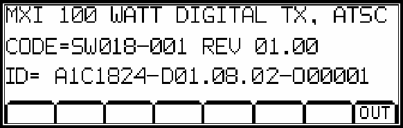
MXi AMPLIFIER CONTROLLER BOARD REV.2
PUB06-82 Rev 1 July 17, 2007 06-82-26 MXi Amplifier Controller Board Rev.2
Figure 16 General Submenu Screen
The eighth menu button is labeled OUT and will cause the LCD screen to return to the Main Menu.
MXi AMPLIFIER CONTROLLER BOARD REV.2
PUB06-82 Rev 1 July 17, 2007 06-82-27 MXi Amplifier Controller Board Rev.2
4 SETUP PROCEDURES
The following sections detail the various set up procedures for the MXi transmitter system. These procedures
should only be done by qualified personnel. If the calibrations and setups are done improperly, it can result in the
transmitter being prone to damage.
The transmitter is normally set up in the factory for the particular operating power required when first installed. Set
up procedures would only be required if certain elements of the MXi transmitter had to be replaced or repaired
that would have affected the calibrations. An example of this would be the MXi controller board itself, the output
RF couplers, the RF cables or the 32V power supply.
If the output power is being changed, then some setup and calibration would be needed since the transmitter
would be set up for the previous RF power level. Caution: do not increase the power output of the MXi transmitter
beyond the original factory set level without first consulting LARCAN field service.
4.1 RF DETECTOR
The RF detector is normally calibrated at the factory or by LARCAN field personnel and should not require onsite
re-adjustments except in the following circumstances.
• The desired output power level of the transmitter is to be changed from the factory setting for a full 100%
power reading. Note that the operator should not just increase and readjust power beyond the
recommended rating of the transmitter without prior approval from LARCAN technical services.
• A replacement MXi control board or directional coupler has been installed in the transmitter.
This procedure assumes that the RF detector is being set-up with the transmitter connected to an RF modulator
input and output load (or antenna) that is the actual configuration it is intended to operate with.
4.1.1 Test Equipment Required
a) An RF power meter such as the HP 436A or similar. For analog transmitters, a BIRD through-line
wattmeter is sufficient.
b) A Spectrum Analyzer, HP 8558B or similar.
If the operator wishes to set up the unit on the bench, then a number of extra pieces of test equipment are
necessary.
• An RF generator/modulator that will replicate the desired signal and level
• An analog transmitter would need a video generator such as Tektronix 1900 or similar
• A modulator such as LARCAN TTC (Catel X - ATM -1600 - 6 - 01/01) or similar.
• An upconverter such as Philips PM 5690 or similar (or one supplied with transmitter)
• A digital transmitter would need the Zenith modulator used with the transmitter. With serial data
input, the Zenith will still generate the appropriate digital spectrum
• An upconverter such as Philips PM 5690 or similar (or one supplied with transmitter)
• RF Load rated at the transmitter power and associated cable
4.1.2 Jumper Installation
If the transmitter is not being upgraded from Analog to Digital service (or vice versa), then there should be no
need to change the jumpers for the traps or gain. If there is a change, the trap jumpers would need to be modified
and perhaps the gain as well.
For Analog service, the color burst and aural carrier traps should normally be installed.
For the forward power sample, this would be jumpers E9 and E10.
For the reflected power sample, this would be jumpers E13 and E14.
MXi AMPLIFIER CONTROLLER BOARD REV.2
PUB06-82 Rev 1 July 17, 2007 06-82-28 MXi Amplifier Controller Board Rev.2
For Digital service, the above four jumpers would not be installed.
If the desired transmitter output power is the same as what the transmitter was originally set up for at the factory,
there should be no need to change the gain jumpers on the RF detectors.
If a change in power is required or the directional coupler has been changed or the transmitter is being moved
between Analog/Digital service, the RF detector should be first set to the lowest possible gain and the jumpers
moved to increase the gain.
For the forward power sample, the gain is controlled by jumpers E8 and E11.
Digital + Low Gain: E8= Av and E11=LO
Digital + High Gain: E8= Av and E11=HI
Analog + Low Gain: E8= Pk and E11=LO
Analog + High Gain: E8= Pk and E11=HI
For the reflected power sample, the gain works identically where E12 is the same as E8 and E15 is the same as
E11.
4.1.3 Verify OpAmp Offsets
1. With no RF signal applied, measure the voltage at TP1 and adjust R58 to make this level under 0.1VDC
2. With no RF signal applied, measure the voltage at TP4 and adjust R80 to make this level under 0.1VDC
4.1.4 Verify Output Power Level
1. Attach the RF output power measuring device (Wattmeter or Average Power Meter) to the RF output.
2. Turn down the drive level of the modulator/upconverter before applying the RF input signal.
3. Turn up the drive level until the output power measures the desired reading. Do not use the meter of the
transmitter itself to determine output power, since at this point it may be uncalibrated.
4. When increasing the power, it is always instructive to measure the current on the 32VDC supply in case
there is a problem with how the output power meter is connected or working. If the supply current is
increasing but the output power is not, set the drive to a sufficiently lower level and double check your
setup.
5. When the RF output power is at the desired level, do the following checks:
a) For the forward power sample, the voltage at TP1 should be within 4.5 to 9.0VDC as a maximum
b) If not, then you have either too much power or too high a coupling in the directional coupler.
6. Reverify the output power: if this is correct, a pad can be inserted between the coupler and J12.
7. Adjust potentiometer R48 until the voltage at TP3 is 4.0VDC.
8. At this point, the meter on the transmitter should read 100%
9. To calibrate the reflected power, install jumper E17 that prevents any VSWR trips
10. Remove the RF cable from J12 and attach a –10dB pad, then connect this reduced forward power
sample to J13.
11. If the original power sample into J12 required a pad, this must be retained in addition to the –10dB pad.
12. For the reflected power sample, the voltage at TP4 should be within 4.5 to 9.0VDC as a maximum
13. If not, reverify that the output power has not changed in the meantime.
14. Adjust potentiometer R80 until the voltage at TP5 is 4.0VDC.
15. At this point, the reflected power meter on the transmitter should read 10.0%.
Note: Make sure that you remove jumper E17 when done, else you will have no VSWR protection!
MXi AMPLIFIER CONTROLLER BOARD REV.2
PUB06-82 Rev 1 July 17, 2007 06-82-29 MXi Amplifier Controller Board Rev.2
At this point, the operator should proceed to verify cutback and VSWR trip functions, as described in the next two
sections.
4.2 AGC AND CUTBACK PROTECTION
Before the operator attempts to set up the AGC or cutback circuitry, the forward and reflected power levels must
be properly set up to calibrated levels as described in Section 4.1.
4.2.1 AGC Setup
The AGC is simply set up using the Amps submenu that is accessed from the Main menu of the LCD. A view of
this submenu is given the below. The operator just needs to press the AGC+ button on the touchpad to increase
the power or the AGC- button to decrease the power. The top line of the LCD displays the current level of the
FWD power. This AGC level will be saved even after AC power outages. If the RF power is nil or very low, make
sure that the RF drive has been enabled by pressing the RF On button on the touchpad
Figure 17 Amps Submenu Screen
4.2.2 Cutback Setup
To set up the cutback level, a power sample must be fed into the reflected power connector of the MXi board that
is –16dB down from the forward power sample level. The most convenient way to accomplish this is to take this
sample from the RF monitor port on the rear of the transmitter chassis.
1. Disconnect the AGC control connector J10 from the MXi board to remove any possible AGC or cutback
action while verifying the Reflected power. If the forward power is greater than 100%, adjust the output
level of the upconverter until it is at 100% (+/- 2%).
2. Attach an RF cable from the RF monitor connector at the rear of the MXi control chassis and insert a
–16dB pad. This pad can consist of a –10dB and –6dB pad in series. Remove the RF cable from J13 that
comes from the output coupler and attach a cable from the –16dB pad off the forward monitor sample.
3. We are assuming that the coupling level from the monitor connector is the same as the coupling level for
the forward power RF coupler. To verify this by checking the RFL power level on the LCD, it should read
around 2.5% power. If it is off by more than 0.5%, adjust the amount of padding until the RFL power
reading is within the range of 2% - 3%. A variable attenuator pad would be ideal for this application.
4. Readjust the upconverter output level so that the forward power reads 110% again.
5. Also disconnect the cable from the monitor port for now.
6. Reconnect the AGC control connector J10 on the MXi board.
7. Reconnect the cable from the monitor port to the reflected power sample at J13.
8. Adjust the potentiometer R105 until the forward power reading is about 96% - 98%, which puts the
system just at the edge of cutback.
The setup is now complete, remove the monitor cable from J13 and attach the output coupler back to J13.
4.3 VSWR PROTECTION
The VSWR protection does not really need any setup or calibration since it is fixed to trip when the reflected
power is –10dB of the forward power level. To verify the VSWR trip function, the following steps must be taken.
MXi AMPLIFIER CONTROLLER BOARD REV.2
PUB06-82 Rev 1 July 17, 2007 06-82-30 MXi Amplifier Controller Board Rev.2
To check the VSWR trips, a power sample must be fed into the reflected power connector of the MXi board that is
–10dB down from the forward power sample level. The most convenient way to accomplish this is to take this
sample from the RF monitor port on the rear of the transmitter chassis.
1. Disconnect the AGC control connector J10 from the MXi board to remove any possible AGC or cutback
action while verifying the Reflected power. If the forward power is greater than 100%, adjust the output level
of the upconverter until it is at 100% (+/- 2%).
2. Install a jumper in E17 that will prevent any VSWR trips.
3. Attach an RF cable from the RF monitor connector at the rear of the MXi control chassis and insert a
–10dB pad. Remove the RF cable from J13 that comes from the output coupler and attach a cable from
the –16dB pad off the forward monitor sample. We are assuming that the coupling level from the monitor
connector is the same as the coupling level for the forward power RF coupler. To verify this by checking
the RFL power level on the LCD, it should read over 10.1% power but less than 11% power. Note that a
minimum of 10.1% power is needed to insure a VSWR trip. If the RFL power is under 10.1%, decrease
the amount of padding until the RFL power reading is within the range. If the RFL power is too high (over
11%), increase the amount of padding until it is in the range. A variable attenuator pad would be ideal for
this application.
4. Readjust the upconverter output level so that the forward power reads 110% again.
5. Also disconnect the cable from the monitor port for now.
6. Reconnect the AGC control connector J10 on the MXi board.
7. Reconnect the cable from the monitor port to the reflected power sample at J13.
8. Remove the jumper from E17 and the transmitter should trip three times and lock out on the fourth trip.
9. The TRIP and Lockout status on the LCD Amps submenu should both be set.
10. The setup is now complete: remove the monitor cable from J13 and attach the output coupler back to
J13.
11. Clear the VSWR lockout and trip condition by either pressing the front panel reset button or issuing a
remote reset command.
4.4 REMOTE CONTROL INTERFACE BAUD
The Remote Control submenu is entered by pressing the RCtl submenu button on the main LCD screen.
This submenu will display all the various parameters that affect the remote controls and the remote RS232 status
communications stream. It will allow the operator to set the baud that is used to communicate with an external
computer. The other parameter that can be adjusted is the number of stop bits.
The LCD displays a typical RCtl submenu as follows:
Figure 18 Remote Control Submenu Screen
The BAUD button on the bottom of the LCD touchpad will cause the baud to increment from the current displayed
baud up to the next higher one. At the same time, the NewFmt light on the third line lights to indicate that a new
serial format (Baud or Stop bits or both) is pending but not taken. Successive pushes of the BAUD button will
cause the baud to increment until it reaches the maximum of 19,200 baud, after which it will roll back to 300 baud,
which is the lowest rate. Note that when setting the baud, if the NewFmt light is on, the rate displayed on the
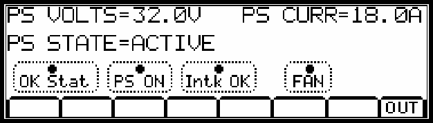
MXi AMPLIFIER CONTROLLER BOARD REV.2
PUB06-82 Rev 1 July 17, 2007 06-82-31 MXi Amplifier Controller Board Rev.2
screen is the new baud that is not yet programmed. Note: The MXi will still operate at the original baud until the
new one is saved.
If the user presses the STOP menu button, then the number of stop bits in the serial format will toggle between
1and 2. The new desired number of stop bits will be displayed in the second line of the LCD within the 8B-1S-NoP
section where the stop bits will be either 1S or 2S in this string. At the same time, the NewFmt light on the third
line lights to indicate that a new serial format (Baud or Stop bits or both) is pending but not taken.
Once the operator is satisfied with the new Baud and Stop bits, pressing the SAVE button causes the MXi to
implement the new serial format. Pressing the CLR button abandons all selections and revert to the previous
Baud and Stop bits without any action taken.
4.5 POWER SUPPLY VOLTAGE AND CURRENT CALIBRATION
To set up the power supply voltage and current reading, the operator must enter the Power Supply submenu on
the LCD. The Power Supply submenu is entered by pressing the P/S submenu button on the main display.
This submenu displays the status, voltage and current for the 32V power supply. Each display item and control is
described as to its meaning and function.
The LCD displays a typical P/S submenu as follows:
Figure 19 Power Supply Submenu Screen
1. To set up the voltage reading, turn on the transmitter and verify that the power supply is indeed running.
Line two of the LCD should have the power supply as active, with all of the status lights in line #3 as true,
just as is shown in the above LCD screen.
2. With a voltmeter, measure the actual voltage from the power supply; this can be measured at pin 1 of J4.
3. Adjust potentiometer R14 until the displayed voltage equals that being measure by the voltmeter.
4. To set up the current reading, the power supply should be ON as in the above paragraph and enough RF
drive (at least 50%) should be applied to get a reasonable current level for calibration.
5. Use a clamp-on current Ampmeter to measure the current draw from the 32V power supply. If multiple
wires are being used to connect the power supply to the RF amplifier, insure that all of the wires are
included in the clamp-on meter. However, make sure that none of the ground wires are included (only the
+32V wires) or else the reading will be too low.
6. If the MXi is configured to measure the current with the onboard current sensor U9 via connector J4,
adjust potentiometer R15 until the displayed current agrees with that measured on the clamp on meter.
If an external power supply is used that has its own current telemetry sensing, it may have its own setup as well.
The current reading on the LCD will still be affected by R15 but the external supply may require its own
calibration, if the level it sends to the MXi is too low or high. A good level would be in the range of 2-4 volts for full
scale current.
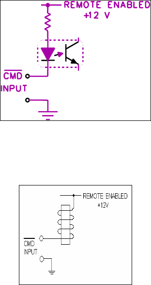
MXi AMPLIFIER CONTROLLER BOARD REV.2
PUB06-82 Rev 1 July 17, 2007 06-82-32 MXi Amplifier Controller Board Rev.2
5 REMOTE CONTROL CONNECTIONS MXi TRANSMITTER
On the rear of the transmitter Chassis, the remote control connections are available on a 15-pin male D-shell
connector J6. This includes all of the remote controls, status and telemetries available to the operator.
These remote signals are routed from the MXi Control board via a 15-wire ribbon cable from connector J6 of the
MXi Control board. The signals designations for each pin of J6 can be viewed on sheet 3 of the schematic in
Figure 26. The actual circuitry that drives these signals is spread out on all five sheets of the schematic.
5.1 REMOTE CONTROLS
The Transmitter MODE must be in REMOTE for any of these remote controls to be operational. The transmitter is
placed in the REMOTE mode via the touch LCD menu options as described in Section 3. The main LCD screen
has a status light to show if the REMOTE MODE is active.
To place the transmitter into REMOTE MODE, the operator must enter the REMCTL submenu on the LCD and
enable the REMOTE MODE.
The MXi provides 4 remote control inputs that effectively replicate the its own front panel mode control buttons.
The VOR (Video Operated Relay) input is not available from the front panel since it is a special type of input that
only makes sense as a remote input.
Figure 20 TX_OFF, RESET, and VOR Remote Controls
The TX_OFF , RESET and VOR remote controls are active low, opto-isolated inputs configured as shown, all of
which require a GROUND for assertion and the activator to be able to sink 15mA or more for at least 200
milliseconds to accomplish reliable keying. Each of these is current-limited by an individual resistor.
Figure 21 TX_ON Remote Control
The TX_ON remote control is an active low input configured to drive a relay coil off +12V supply. It requires a
GROUND for assertion and the activator to be able to sink 100 mA or more for at least 200 milliseconds to
accomplish reliable keying.

MXi AMPLIFIER CONTROLLER BOARD REV.2
PUB06-82 Rev 1 July 17, 2007 06-82-33 MXi Amplifier Controller Board Rev.2
TX D-Connector PC Board Connector Designation Description
Remote Control
Pin 1 J6 Pin 1 RC_TX_On Turns Transmitter ON
Pin 9 J6 Pin 2 RC_TX_Off Turns Transmitter OFF
Pin 2 J6 Pin 3 RC_Reset Resets VSWR Trip
Pin 4 J6 Pin 7 RC_VOR VOR On Controls
Pin 12 J6 Pin 8 Ground Ground Reference
Pin 15 J6 Pin 14 EXT1+ Secondary Ext1 Intk
Pin 8 J6 Pin 15 EXT1– Secondary Ext1 Intk
5.1.1 RC_TX_On Remote Transmitter ON Control
The MXi controller has the facility to force the ON/OFF function to follow the front panel ON button. Jumper E5 is
a two-position jumper that can be placed in the EXT or INT position (these are silk screened on the PC board).
When in the INT position and the front panel button is the ON position, this will force the transmitter to the ON
state regardless of the remote or CPU controls. If the front panel button is the OFF position, then the remote ON
command will function normally. When jumper E5 is in the EXT position (normal state), then the remote ON
command will function normally as well.
A second jumper E7 (Manual Control) also affects the remote ON commands. When installed, this jumper
effectively bypasses the CPU and the REMOTE MODE. The transmitter will turn ON whenever there is a low
signal applied to the RC_TX_On command input. When this signal is removed, the transmitter turns OFF. This
jumper is really a Bypass of the CPU’s remote control function and is only meant for emergency purposes. In
normal operation, jumper E7 would not be installed. Also note that if jumper E5 (mentioned above) is in INT and
the front panel ON button is in the ON position, the remote control input will not be able to turn OFF the
transmitter, since it is being held on by the front panel pushbutton.
The following description assumes that jumper E5 is in the EXT position and jumper E7 is not installed.
An active low signal applied to the RC_TX_On command input causes the CPU to read this active state and if the
transmitter is in REMOTE mode, then the CPU will issue an ON command to the ON relay K1.
Note that this changes the transmitter’s state to ON (when in REMOTE) such that after any subsequent power
outage, the MXi transmitter will return to its previous state.
If the operator changes the transmitter’s MODE from REMOTE to LOCAL, the ON/OFF state of the transmitter will
be controlled by the position of the front panel ON/OFF button.
If the operator changes the transmitter’s MODE from LOCAL to REMOTE, the ON/OFF state of the transmitter will
revert to the previous state when REMOTE MODE was active.
5.1.2 RC_TX_Off Remote Transmitter OFF Control
The following description assumes that jumper E5 is in the EXT position and jumper E7 is not installed.
An active low signal applied to the RC_TX_Off command input causes the CPU to read this active state and if the
transmitter is in REMOTE mode, the CPU removes the ON command from the ON relay K1.
Note that this changes the transmitters state to OFF (when in REMOTE) such that after any subsequent power
outage, the MXi transmitter will return to its previous state.
If the operator changes the transmitter’s MODE from REMOTE to LOCAL, the ON/OFF state of the transmitter will
be controlled by the position of the front panel ON/OFF button.
If the operator changes the transmitter’s MODE from LOCAL to REMOTE, the ON/OFF state of the transmitter will
revert to the previous state when REMOTE MODE was active.
MXi AMPLIFIER CONTROLLER BOARD REV.2
PUB06-82 Rev 1 July 17, 2007 06-82-34 MXi Amplifier Controller Board Rev.2
5.1.3 RC_TX_VOR Remote Transmitter VOR Control
The following discussion is assuming that jumper E5 is in the EXT position and jumper E7 is not installed.
The VOR (Video Operated Relay) control is a specialize input that performs a very rudimentary control of a
network of transmitters. The VOR is a signal that is active when video has been present for a specified length of
time, typically around 30 seconds or longer. The presence of video for more than this time causes the CPU to
issue an ON command to the ON relay K1.
When video disappears for more than a shorter amount of time, typically around 5 seconds, the CPU removes the
ON command from the ON relay K1.
This is used when full remote controls are not available for transmitters located in areas that are difficult to
access. In this manner, the operator can turn ON or OFF any number of transmitters in the network by either
applying (or removing) video at the source feed. When this VOR control is being used, the normal remote ON or
OFF commands would not be utilized.
Note that this changes the transmitter’s state to ON (when in REMOTE) such that after any subsequent power
outage, the MXi transmitter returns to its previous state.
If the operator changes the transmitter’s MODE from REMOTE to LOCAL, then the ON/OFF state of the
transmitter will then be controlled by the position of the front panel ON/OFF button.
If the operator changes the transmitter’s MODE from LOCAL to REMOTE, the ON/OFF state of the transmitter will
revert to the previous state when REMOTE MODE was active.
5.1.4 RC_RESET Remote RESET Control
The remote reset command can have four different possible operations depending on which jumpers are selected
in the MXi board.
If both jumpers E18 and E2 are removed (this is the normal mode), the reset command is fed only to the CPU
chip, which then issues a VSWR reset, only if the MXi system is in Remote Mode.
If jumper E18 is installed but E2 is removed, the reset command is manually routed to the VSWR relay reset coil and
effectively bypasses the CPU chip. In this configuration, a remote reset command clears the VSWR relay and does
not depend on the MXi being in Remote Mode.
If jumper E18 is out but E2 is installed, the remote reset command first causes a reset of the CPU chip itself and, if
the MXi system is in Remote Mode, the CPU will itself then issue a VSWR reset command.
If both jumper E18 and E2 are installed, the remote reset command causes a reset of the CPU chip itself and will be
manually routed to the VSWR relay reset coil bypassing the CPU chip.
5.2 EXT1 SECONDARY EXTERNAL #1 INTERLOCK
The remote connector also has a pair of contacts that replicate a parallel set of contacts for the EXT1 interlocks at
TB1 on the rear panel. This is not really a remote control, but it could be used as a simple ON/OFF by supplying a
set of controlling contacts across EXT1+ and EXT1–. There is no real polarity required and the + and –
designations are just to differentiate the two pins. The other set of contacts on TB1 should be left unconnected if
this is being used.
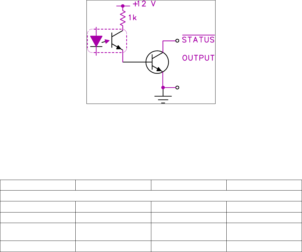
MXi AMPLIFIER CONTROLLER BOARD REV.2
PUB06-82 Rev 1 July 17, 2007 06-82-35 MXi Amplifier Controller Board Rev.2
5.2.1 Status Outputs
Figure 22 Status Outputs
These are current sinking open collector outputs, out of quad pack MPQ2222 (2N2222A) NPN transistors driven
by opto-isolator devices. The available output sink current is dependent on the gain of the NPN and the opto-
isolator transfer ratio. Generally, one can expect at least 100mA of sinking current for each output listed here.
Because these are open collector, they can be used in special applications, such as on-site warning signal
activation if desired, but they are limited in external circuit voltage to maximum 60VDC. Each status (in
parentheses) indicates what it means when in its active low condition.
The MXi provides three remote control outputs that represent the current operating state of the switching system
via the Digital Output Board
TX D-Connector PC Board Connector Designation Description
Remote Control
Pin 9 J6 Pin 2 RS TXOn Transmitter is turned ON
Pin 2 J6 Pin 3 RS_Error Transmitter has an error
Pin 10 J6 Pin 4 RS_Remote Transmitter is in Remote
Mode
Pin 12 J6 Pin 8 Ground Ground Reference
5.3 TELEMETRY OUTPUTS
These are buffered OpAmp outputs, out of quad pack LM324 operational amplifiers. The available output voltage
is limited to the range of 0 – 5VDC. The OpAmp can reliably source around 5mA of current and so a relatively
high impedance input of at least 2K ohms should be used. Each telemetry has a description to indicate what
parameter it is measuring.
The MXi provides five remote telemetry outputs that represent the current operating levels of the MXi transmitter.

MXi AMPLIFIER CONTROLLER BOARD REV.2
PUB06-82 Rev 1 July 17, 2007 06-82-36 MXi Amplifier Controller Board Rev.2
TX D-Connector PC Board Connector Designation Description
Remote Controls
Pin 5 J6 Pin 9 RT_FWD Forward RF power level
Pin 13 J6 Pin 10 RT_RFL Reflected RF power level
Pin 6 J6 Pin 11 RT_AUR Aural RF power level
(optional)
Pin 15 J6 Pin 12 RT_AGC AGC voltage (1/2 scale)
Pin 7 J6 Pin 13 RT_CUTB Cutback voltage (1/2
scale)
Pin 12 J6 Pin 8 Ground Ground Reference
MXi AMPLIFIER CONTROLLER BOARD REV.2
PUB06-82 Rev 1 July 17, 2007 06-82-37 MXi Amplifier Controller Board Rev.2
6 CIRCUIT DESCRIPTIONS
6.1 MC68HC908 MICROPROCESSOR
The Motorola MC68HC908GT microprocessor (often referred to as the CPU or HC08) performs all of the control
interface and communications in the MXi transmitter system. It is a 44-pin surface mount PLCC type device that is
permanently soldered to the circuit board and is not field serviceable or easily replaced without special surface
mount tooling. A brief description of the part is given in this section and a portion of the manufacturer’s
documentation is given in Appendix A. More detailed information on this part can be obtained from the Motorola
web site.
The HC08 chip used in the MXi can come with either 8K or 16K bytes of non-volatile flash memory, which can be
erased and reprogrammed to allow updating of software code or system parameters. The MXi code is typically
smaller than 8k and so would fit in either size of Flash memory. The HC08 chip has a dedicated serial input pin
designated as the BDM (Background Debug Mode) port that is used to program the internal Flash memory and
for debug testing. The MXi is programmed at the factory and it is not expected that reprogramming would need be
done in the field, although it is possible to do with the proper software. System parameters and status that need to
be retained during power failures (such as the LOG entries) are also stored in the Flash memory.
Most of the external pins on the HC08 are configured as programmable Input/Output (I/O) ports, where the
software program determines whether a certain pin is to be configured as either an input or output. The pins on
the HC08 are grouped together in sets called PORTs. These Ports will have eight pins (or fewer) to support the
byte wide data path in the CPU. Port A is used for general system inputs and outputs. Port B is used as an eight-
channel A/D converter to measure system telemetry values. Port C is used for general system inputs and outputs.
Port D assigns four pins for the synchronous serial port (SPI) with the other four pins used for system inputs. Port
E assigns two pins as a serial communications port (SCI), one pin is the external CPU clock and the other two
pins used for general system inputs and outputs.
The definition of each Port pin is as follows:
PORT A
PA0 Input or Output Jumper E3 configures as I/P or O/P
PA1 Input Remote Control ON Command
PA2 Input Remote Control OFF Command
PA3 Output Select enable for Serial NvPot U16
PA4 Input Front Panel ON Command
PA5 Input Front Panel VSWR RESET Command
PA6 Input 32V Power Supply OK Status
PA7 Input Remote Control VOR Status
PORT B
PB0 Telemetry Temperature of Heatsink [Optional]
PB1 Telemetry Power Supply Current
PB2 Telemetry Power Supply Volts
PB3 Telemetry Cutback Volts [Scaled at half the actual value]
PB4 Telemetry AGC Volts [Scaled at half the actual value]
PB5 Telemetry RF Aural Power [from RF detector - Optional]
PB6 Telemetry RF Reflected Power [from RF detector]
PB7 Telemetry RF Forward Power [from RF detector]
MXi AMPLIFIER CONTROLLER BOARD REV.2
PUB06-82 Rev 1 July 17, 2007 06-82-38 MXi Amplifier Controller Board Rev.2
PORT C
PC0 Output Remote Status – Error
PC1 Input DipSw #1
PC2 Input Power Supply (Relay K1) ON Status
PC3 Input DipSw #2
PC4 Input External #1 Interlock
PC5 Output VSWR Reset Control
PC6 Output PS ON Ctl +12V out [could be 24V too]
PORT D
PD0 SPI SS Used by UART
PD1 SPI MISO Used by UART and NvPot
PD2 SPI MOSI Used by UART and NvPot
PD3 SPI SCLK Used by UART and NvPot
PD4 Input Fan#1 Status, Active Low
PD5 Input Fan#2 Status, Active Low
PD6 Input Fan#3 Status, Active Low
PD7 Input Fan#4 Status, Active Low
PORT E
PE0 SCI Transmit Data Used by LCD
PE1 SCI Receive Data Used by LCD
PE2 O/P Remote Status – Remote Mode
PE3 Input VSWR Trip Status
PE4 System Main CPU Clock – 4.9152MHz
The HC08 provides two separate serial interfaces to external components, these are the synchronous peripheral
interface (SPI) and the serial communications interface (SCI).
The SCI implements the standard three-wire serial port (Rx Data, Tx Data and Ground) that would interface to a
typical computer port. The baud is settable from 300 up to 38,400 bits per second via the LCD menus. The baud
is derived from the system oscillator clock at 4.9152MHz. This frequency is recommended by the manufacturer to
easily obtain the most common bauds.
The SPI implements a four-wire clocked serial port that has four signals, Slave Select (SS), Master Out Slave In
(MOSI), Master In Slave Out (MISO) and Serial Clock (SCLK). The HC08 is always set as the Master who
initiates all serial communications. The SPI port is used to communicate with the MAX3110 UART (U2) and the
DS1867 NovPot (U16). The HC08 will send out it data stream from the MOSI line and reads any responses from
the external (Slave) devices via the MISO line. The SCLK is a serial clock (set for around 64K baud) that
synchronizes the data transfer. The presence of this clock allows must higher data rates than the asynchronous
SCI serial protocol. The SS line is a select that enables the MAX 3110 UART when low. A second individual
select line from Port A (pin PA3) is used to select the DS1867 NovPot.
6.2 POWER SUPPLY VOLTAGE AND CURRENT MONITORING
For the following description, refer to Figure 25 (Sheet #2 of the Schematic) in the upper section of the drawing for
the power supply monitoring circuitry.
MXi AMPLIFIER CONTROLLER BOARD REV.2
PUB06-82 Rev 1 July 17, 2007 06-82-39 MXi Amplifier Controller Board Rev.2
The MXi board has a built-in Hall Effect current sensor that is able to measure the current drawn by the RF
amplifier from the +32 volt power supply. The standard MXi low power transmitter would have a 25 amp current
sensor. There are two possible sensors that could be installed in the MXi which depend on the actual current level
that is to be measured. A higher power MXi transmitter would be fitted with a 40 amp current sensor. For higher
power transmitters, the power supply would be external to the amplifier chassis and is fitted with its own current
sensor telemetry that is fed into the MXi board separately and the MXi current sensor would be left unused.
Another consideration for making the current sensor external on higher power MXi transmitters is the gauge of
wire required for these higher current make it difficult to wire into the MXi board connector J4.
The circuit board has winding jumpers E20-E23 that allow a single input winding to the current sensor or a dual
winding input to the current sensor. These winding jumpers allow for lower power transmitters (which require
lower power supply currents) to generate a reasonable output voltage from the current sensor. When the winding
jumpers are in the low current setting (“Lo I” = E20 jumpered to E21), this causes the input current to pass
through the input of the current sensor twice (in two windings) producing double the output voltage than would be
generated by a single winding. This is used for lower power transmitters where the maximum power supply
current draw is under half of the rating of the current sensor.
When the winding jumpers are in the high current setting (“Hi I” = E20 jumpered to E22 and E21 jumpered to
E23), this causes the input current to pass through the input of the current sensor only once (in one winding)
producing half the output voltage than would be generated by a double winding. This is used for higher power
transmitters where the maximum power supply current draw is over half of the rating of the current sensor.
When the internal current sensing is being utilized, the MXi expects the +32V to be applied at connector J4 pin 1.
This voltage is passed through a current monitoring circuit and then fed back out on pin 2 of J4 to the RF
amplifiers. The Hall Effect Sensor U9 has a built in voltage reference of 2.5 volts. The sensing output would be at
this 2.5V level when there is no current through the sensor. When current passes through the sensor, then the
output voltage would either increase or decrease from the 2.5V reference. Whether the voltage increases or
decreases depends on the direction of current flow through the sensor thus making this device bi-directional. In
our configuration, the current only flows one way and increasing current will result in decreasing sensor output
voltages. Jumper E4 selects between the internal U9 2.5V reference or an external current sensor. When using
U9 as the sensor, jumper E4 must be placed in the INT position. The output of E4 is fed into the positive input of
OpAmp U7B with the negative input fed from the U9 sensing output such that the OpAmp effectively removes the
2.5V offset introduced by the U9 sensor. A potentiometer R15 is placed in the feedback path of U7A to allow the
current to be calibrated.
When the power supply is external (usual in higher power MXi transmitters), the actual power supply is external to
the amplifier chassis and will then do its own current metering. In this configuration, the MXi board would not have
its own U9 current sensor installed but would receive this telemetry information from J5 pin 5. Jumper E4 selects
between the internal U9 sensing output or an external current sensor. When using the external sensor, jumper E4
must be placed in the EXT position. OpAmp U7A allows for a gain control through potentiometer R15 so that the
current reading can be calibrated.
The Power Supply voltage is expected to be +32 volts DC +/- 0.5V and can be fed into the MXi board from one of
two points, depending on whether the supply is internal or external to the amplifier chassis.
When the power supply is internal to the MXi amplifier chassis, then the MXi expects the +32V to be applied at
connector J4 pin 1. This voltage is passed through a current monitoring circuit and then fed back out on pin 2 of
J4 to the RF amplifiers. This configuration is used when the MXi is a lower power transmitter that can
accommodate the power supply internally.
When the power supply is external (usual in higher power MXi transmitters), the actual power supply is external to
the amplifier chassis and will then do its own current metering. The +32V sample is connected to J5 pin 6 (which
is in parallel with J1 pin 1). Connector J1 is a higher current contact that would allow the current to be passed
through the internal current sensor U9. For an external supply these are not required and so both U9 and J4 will
most likely not be installed on the board.
MXi AMPLIFIER CONTROLLER BOARD REV.2
PUB06-82 Rev 1 July 17, 2007 06-82-40 MXi Amplifier Controller Board Rev.2
6.3 ON/OFF RELAY K1
The ON/OFF relay K1 and associated circuitry is shown in Figure 25. Relay K1 is a four-pole, single-side stable
relay that requires a constant voltage applied to its coil to maintain contact closure. The contacts of this relay
provide the control signals to activate the +32V power supply and the cooling fans.
There are two elements that determine if power is applied to the coil of K1. One is the +12V arming voltage on the
positive side of the coil that comes from the interlock chain. Four interlocks are placed in series with this coil such
that all four must be closed in order for K1 to receive its +12V arming voltage. The four interlocks are Thermal, Tx
Switching, External #1 and VSWR Trip. If any of these interlocks are open, then the relay will not be energized
and transmitter amplifier will be shut down.
The second element that determines if power is applied to the coil of K1 is the control signal on the negative side
of the coil. Note that LED DS5, which can be seen on the MXi front panel, indicates that the ON control signal has
been issued to relay K1. This control signal can come from one or more of three sources.
The HC08 CPU can always activate the coil from its PC6 pin. This pin activates the base of transistor U10B that
in turn will energize the coil of K1. The second source is the remote control TX_ON command at connector J6 pin
1. When jumper E7 is installed, the remote control TX_ON command can directly energize the coil of K1. The
third source is the front panel ON button. When jumper E5 is in the INT position, the front panel ON button when
pressed in will directly energize the coil of K1.
When K1 is energized, all four poles of the relay will close and cause the transmitter to generate RF power.
Two poles are connected in parallel and send +12V (or +24 volts in some applications) to the fans at connector
J8. Two poles are used since the current rating of one relay pole is not sufficient for the total current draw of up to
four fans. One pole is used to send a +12V command to the +32V power supply. This command causes the
power supply to activate and send its +32V to the RF amplifier. The last pole is used for status, when closed a
ground is sent to the remote control status output RS_TX_ON at J6 pin 5. When K1 is not energized, the ground
of this pole is sent back to the HC08 which uses this input to determine if the relay K1 is energized or not.
6.4 AGC, CUTBACK AND VSWR
Figure 28 shows the circuitry associated with the AGC, cutback and VSWR functions. Each of these is described
as follows.
The AGC circuit uses the voltage reference that is set by the HC08 CPU via the NvPot U16 pin 13. This voltage is
effectively the desired voltage output that the system wants to see coming from the forward power RF detector.
OpAmp U15A compares the U16 reference voltage to the actual voltage from the RF detector and provides an
error output voltage when the value of the detected voltage is greater than the desired reference. If the detected
voltage is less, then we have lower power than is desired and no AGC action would be needed. The OpAmp 15A
has a high value feedback resistor to provide high gain and cause a strong AGC action for relatively small
changes in output power.
The output error voltage from U15A is fed through a resistor divider that has jumper E16 in the middle of it. If E16
is installed, this shorts out any error voltage from U15A and disables the AGC action. This jumper should not be
normally left installed, it is typically only used during setup operations and should be removed for everyday
operations.
If E16 is not installed, the AGC error voltage is fed to the input of buffer OpAmp U15D and then out the MXi
control board to the RF PreAmp attenuator via connector J10. The voltage at the PreAmp reduces the drive level
to the RF amplifier and thus reduces the output power.
The AGC error voltage from U15A is divided by two with resistor divider R90/R92 and sent to the inputs of buffer
OpAmps U15B and U15C. U15B provides AGC voltage telemetry for the remote control and U15C provides AGC
voltage telemetry for the HC08 CPU that is displayed on the LCD.
The Cutback circuitry monitors the level of reflected power and compares it to a preset level. If the reflected power
exceeds the reference level then an AGC voltage is produces that reduces the transmitter output power. The
purpose for doing this is to protect the Amplifier devices from damage resultant from too much RF power
reflecting back from the output system.
MXi AMPLIFIER CONTROLLER BOARD REV.2
PUB06-82 Rev 1 July 17, 2007 06-82-41 MXi Amplifier Controller Board Rev.2
The reflected power sample is send to OpAmp U17C which compares this with the reference level set by
potentiometer R15 and test point TP6. This reference level is set up by sending –16dB of the transmitter forward
power into the reflected port and adjusting R105 until the MXi begins to just start reducing the transmitters output
power.
When the reflected power exceeds the reference level, OpAmp U17C will generate an error voltage that is fed into
the AGC output OpAmp U15D via diode CR12. This has the same effect as an AGC reduction.
The Cutback voltage from U17C is divided by two with resistor divider R98/R99 and sent to the inputs of buffer
OpAmps U19B and U19A. U19A provides Cutback voltage telemetry for the remote control and U19B provides
Cutback voltage telemetry for the HC08 CPU that would be displayed on the LCD.
The VSWR trip circuit provides protection to the RF amplifier in the presence of a persistent and high level
reflected power condition. The VSWR system is set to trip at a reflected power level of –10dB down from the
forward power.
OpAmp U17 compares the reflected power voltage with the forward power voltage. When the RF detector setup is
done, the reflected power voltage is set for 4.0V when it is at a level of –10dB lower that the full rated forward
power. The forward power voltage is set for 4.0V when it is at the full rated forward power level. When these two
voltages are equal, then the reflected power is indeed –10dB under the forward power level.
In the case that the forward power sample has been removed or improperly setup, it is possible for the forward
power level to be near 0V or very low. In this condition, any amount of reflected power would cause a VSWR trip
which is undesirable and unnecessary. To prevent this event, OpAmp U17B forces a minimum forward power level
of about 1.5V into U17D that would require a minimum reflected voltage of 1.5V to cause a VSWR trip. This
represents a reflected power level of around –8.5dB instead of –10dB.
When the reflected level exceeds –10dB, set coil of relay K2 is energized, causing a VSWR trip to occur. Relay K2 is
a two-coil latched relay where energizing the set coil causes the contacts of K2 to move into the set position and
remain there even after the coil is de-energized. Once a VSWR trip has occurred, the relay K2 will remain in the set
position until a signal is sent to the other reset coil that moves the contacts back into the original clear position.
The relay K2 can be reset from one or more of three sources.
The HC08 CPU can always activate the coil from its PC5 pin. This pin forces the output of NAND gate U18A high
which activates the base of transistor U6C that in turn will energize the reset coil of K2. The second source is the
remote control RC_RST command at connector J6 pin 2. When jumper E18 is installed, the remote control RC_RST
command can directly drive the base of transistor U6C that in turn will energize the reset coil of K2. The third source
is the front panel RESET button. When the front panel RESET button is pressed in, it directly energizes the reset coil
of K2.
The VSWR relay has two poles, one for the transmitter interlock and the second for status. The interlock pole is part
of the arming interlock chain of the ON/OFF relay K1. If the K2 contact is opened (i.e., there was a VSWR trip), the
arming voltage is removed from ON/OFF relay K1 and the transmitter shuts down. Note that jumper E17 is provided
to override the VSWR relay trip contacts. This jumper is only for setup purposes and should never be left installed in
normal operations.
Note: Leaving the jumper E17 installed will defeat all the VSWR protection and could result in damage to the RF
amplifier if a high reflected power condition occurs.
The second pole of K2 lights status LED DS10 when the relay has tripped under VSWR condition. The other side of
this pole is fed into the CPU, which uses this to determine if K2 is tripped or not.
6.5 SPI UART
The Maxim MAX3110 is a full single channel serial UART with integral RS232 drivers and receivers. The device
uses the SPI interface to communicate with the HC08 CPU. A brief description of the part is given in this section
and a portion of the manufacturers documentation is given in Appendix A. More detailed information on this part
can be obtained from the Maxim/Dallas Semiconductor web site.
This device can implement a full serial port with data and handshaking lines. In this application, the handshaking
lines are not used and these inputs/outputs are used for general signal purposes. The RTS output is used as a
remote control TX_FAIL output status and the CTS input is used to read the Thermal Interlock status.
MXi AMPLIFIER CONTROLLER BOARD REV.2
PUB06-82 Rev 1 July 17, 2007 06-82-42 MXi Amplifier Controller Board Rev.2
The UART has its own 1.8432MHz crystal to generate the appropriate bauds. The CPU program sets up the baud
as 9600 as the default but this can be altered by user command via the LCD touchpad menus.
An interrupt line is provided by the UART to signal the HC08 CPU when it is available for more data to transmit or
when new data has been received. The device can also interrupt the HC08 in the presence of certain types of
serial transmission error conditions.
The HC08 uses all four of the SPI interface lines to communicate with the UART, since it must both send data to
the UART that must be transmitted and must read data from the UART that has been received. The CPU output
Slave Select (SS) line is used to enable SPI communications with the UART. The HC08 has assigned the UART
to provide communications between the HC08 and the LCD unit.
The UART has two RS232 drivers and two RS232 receivers that will translate the RS232 level to CMOS/TTL
levels. One driver/receiver pair is used to interface the UART serial data to the LCD. The second driver/receiver
pair is used to interface the HC08 serial data to the external computer.
6.6 SPI NVPOT
The Dallas Semiconductor DS1867 NvPot (non-volatile Potentiometer) dual channel serial potentiometer with
data retention on power down. The device uses the SPI interface to communicate with the HC08 CPU. More
detailed information on this part can be obtained from the Dallas Semiconductor website.
This device implements two independent variable resistances whose value is controlled by data bytes sent by the
HC08 to the NvPot device. These resistances can be varied from close to 0 ohms up to 10k ohms in 256
individual steps (each step would be about 40 ohms each). The NvPot device retains these settings in non-volatile
memory so that they can be restored after a power outage. Figure 24 and Figure 28 show the HC08 CPU and the
NovPot circuitry.
The HC08 only uses two of the SPI interface signals to communicate with the NvPot. The MOSI signal is used to
send data to the NvPot (there is no need to receive any data from the device so MISO is not used).
The SCLK is used to provide the synchronization clock. A separate select line PA3 is used to enable
communications to the device. When PA3 is low, the NvPot communications is disabled and when PA3 is high the
NvPot communications is enabled. The HC08 must co-ordinate the selects between this NvPot and the UART
that share the SPI data line. The select lines are set such that only one of these devices are active at one time.
One of the variable resistance potentiometers is used by the HC08 to set the AGC reference voltage that drives
the AGC circuitry in Figure 28.
The second potentiometer is used to calibrate the thermistor temperature reading from the heatsink. Note that the
thermistor is an optional component and may not be present in all MXi transmitters.
6.7 RF DETECTOR
6.7.1 Circuit Description
The board is fitted with two RF detectors, which respond to RF samples fed from RF directional couplers mounted
on output combiner of the Amplifier heatsink. The modulation envelope blanking level is measured because it
remains constant, regardless of the picture content of the transmission. Measurement occurs during the back
porch. Both sections of the board are configured in a similar way.
6.8 J12 CHANNEL – VISUAL FORWARD
The RF sample is applied to input J12 and is terminated by R52 in parallel with R53 for an impedance of around
50 ohms. CR5 and Q4 form an envelope detector. CR5 is forward biased slightly by R43 and R54 to overcome
CR5 conduction threshold voltage, thereby improving detection linearity. Q4 is forward biased by R43 as well, and
when RF is applied, Q4 is driven in the direction of turn off during each positive-going half cycle, thus causing its
emitter voltage to become more positive and in effect forming a linear envelope detector.
C24 utilizes the lead inductances of CR5 and Q4 to form a Tee network, which provides a matching section that
improves the UHF signal transfer between the devices. Q4 and CR5 have similar temperature coefficients and the
opposing connection of the two in this back-to-back configuration provides temperature compensation.
MXi AMPLIFIER CONTROLLER BOARD REV.2
PUB06-82 Rev 1 July 17, 2007 06-82-43 MXi Amplifier Controller Board Rev.2
Finally, Q4 serves as a low impedance video source. Jumper E9 is used to introduce color subcarrier trap FL1. An
alternate trap consisting of C43, C25 and L1 (marked with asterisks) can also provide this function. The alternate
trap can also be easily changed in values to provide different frequency traps for other systems (like PAL).
Note: only one of either FL1 or the Inductor/Capacitor traps would be installed but never both.
Transistor Q2 serves as a buffer and Q1 serves as another buffer. Following is filter FL2, which removes the aural
carrier. An alternate Inductor/Capacitor trap consisting of L2, C44 and C26 is also provided.
The inverted and amplified video signal is fed to a peak detector comprised of CR4, C22 and R47 through either
resistor R42 (1k ohm) or resistor R46 (33 ohm). Jumper E8 will determine which resistor is in the path and is silk
screened as Pk (peak) or Av (average) on the circuit board. If the RF signal is Digital, then E8 is installed in the
Av position where R42 will effectively form a RC charging circuit that averages the signal and eliminates any
momentary peaks. If the RF signal is analog, then E8 is installed in the Pk position, where R46 will effectively
pass the entire detected envelope to the peak detector.
Because a single supply op-amp is used at U5, the output seen on TP1 and TP2 contains a small DC offset which
must be minimized because low level signals are near ground/earth potential. With no RF input, this offset voltage is
adjusted by potentiometer R58 as near as possible to ground/earth. The setting can be seen when using a DC
coupled scope. Adjust R58 to move the DC level toward ground/earth potential; stop turning the potentiometer
immediately the DC ceases moving. A residual voltage offset of 20 millivolts can be expected for the LM358 family of
op-amps.
The gain of the amplifier stage at U5A can be adjusted by selecting one of the two available feedback resistors R56
(5.1K ohms) or R59 (10K ohms) using jumper E11. When a lower gain is desired, E11 is placed in the LO position
selecting R56 and when a higher gain is desired, E11 is placed in the HI position selecting R59.
The two test points TP1 and TP2 are provided to support the external aural detector. When this option is not
installed, a jumper is placed between J11 pin 5 and J11 pin 6 which placed these two test points at the same
potential.
Outputs from unity gain op-amps U13A, U13B, U13C and U13D drive the forward power metering circuits. The
output of U13A provides telemetry to the CPU A/D converter input. The output of U13B provides telemetry to the
AGC (VSWR) circuitry. The output of U13C provides telemetry to the remote controls and U13D provides telemetry
for the optional transmitter switch connections. Bench test calibration consists of adjusting R48 with rated, properly
modulated input while observing the voltage at TP3, which should read 4.0 volts DC for full scale calibration.
6.9 J13 CHANNEL – REFLECTED
The RF sample is applied to input J13 and is terminated by R74 in parallel with R75 for an impedance of around
50 ohms. CR9 and Q6 form an envelope detector. CR9 is forward biased slightly by R67 and R76 to overcome
CR9 conduction threshold voltage, thereby improving detection linearity. Q6 is forward biased by R67 as well, and
when RF is applied, Q6 is driven in the direction of turn off during each positive-going half cycle, thus causing its
emitter voltage to become more positive and in effect forming a linear envelope detector.
C32 utilizes the lead inductances of CR9 and Q6 to form a Tee network, which provides a matching section that
improves the UHF signal transfer between the devices. Q4 and CR5 have similar temperature coefficients and the
opposing connection of the two in this back-to-back configuration provides temperature compensation.
Finally, Q6 serves as a low impedance video source. Jumper E13 is used to introduce color subcarrier trap FL3.
An alternate trap consisting of C33, C45 and L3 (marked with asterisks) can also provide this function. The
alternate trap can also be easily changed in values to provide different frequency traps for other systems (like
PAL). Note that only one of either FL1 or the Inductor/Capacitor traps would be installed but never both.
Following is filter FL4 which removes the aural carrier. An alternate Inductor/Capacitor trap consisting of L4, C46
and C32 is also provided.
The inverted and amplified video signal is fed to a peak detector comprised of CR8, C30 and R71 through either
resistor R66 (1k ohm) or resistor R70 (33 ohm). Jumper E12 will determine which resistor is in the path and is silk
screened as Pk or Av on the circuit board. If the RF signal is Digital, then E12 is installed in the Av position where
R66 will effectively form a RC charging circuit that averages the signal and eliminates any momentary peaks. If
the RF signal is analog, then E12 is installed in the Pk position where R70 will effectively pass the entire detected
envelope to the peak detector.
MXi AMPLIFIER CONTROLLER BOARD REV.2
PUB06-82 Rev 1 July 17, 2007 06-82-44 MXi Amplifier Controller Board Rev.2
Because a single supply op-amp is used at U14D, the output seen on TP4 will contain a small DC offset which must
be minimized because low level signals are near ground/earth potential. With no RF input, this offset voltage is
adjusted by potentiometer R80 as near as possible to ground/earth. The setting can be seen when using a
DC-coupled scope. Adjust R80 to move the DC level toward ground/earth potential; stop turning the potentiometer
immediately the DC ceases moving. A residual voltage offset of 20 millivolts can be expected for the LM358 family of
op-amps.
The gain of the amplifier stage at U14D can be adjusted by selecting one of the two available feedback resistors
R79 (6.2K ohms) or R82 (20K ohms), using jumper E15. When a lower gain is desired, E15 is placed in the LO
position selecting R79 and when a higher gain is desired, E15 is placed in the HI position selecting R82.
Outputs from unity gain op-amps U14A, U14B and U14D drive the reflected power metering circuits. The output of
U14A provides telemetry to the CPU A/D converter input. The output of U14B provides telemetry to the CUTBACK
and VSWR circuitry. The output of U14C provides telemetry to the remote controls. Bench test calibration consists of
adjusting R72 with rated, properly modulated input while observing the voltage at TP5, which should read 4.0 volts
DC for full scale calibration.
6.10 J12 CHANNEL – AURAL FORWARD
Note: This description only applies when the aural metering option has been included in the transmitter system.
The aural metering circuit takes a sample of detected video signal from the forward port and provides DC level
proportional to the amplitude of the aural carrier. The sample of this DC level is used to compensate visual
forward reading affected by presence of the aural carrier at the forward port.
The inverted and amplified video signal is fed to sync separator U9-2. When sync is detected, the sync output at
pin 1 delivers a positive-going composite sync pulse, which turns on Q11 whose collector then goes LOW. If no
sync is detected by U9, its pin 1 remains LOW and Q11 remains off.
After U9-1 pulse has finished, Q11 turns off and its collector output goes HIGH. This LOW to HIGH transition
activates blanking multivibrator U7 and an active low pulse is fed to Q10, turning it on.
Q2, C4, and U2A form a sample-and-hold circuit that samples the signal originating from the emitter of Q1 and which
is buffered by Q18. Sampling occurs during the back porch, and holds during the subsequent horizontal line. This
DC sample is amplified in U2A .
The sample of the signal detected by CR1 from J1 port is buffered by Q3. The wideband visual/aural signal drives
an aural bandpass ceramic filter FL3. The filter is chosen for the broadcast standard in use. C12 couples the
filtered aural CW signal to amplifier Q7. Following is a buffer Q6 and RF amplifier U4. The aural signal from U4
output is then fed to peak detector consisting of CR2, C15, R45. Q8 buffers signal before applying to sample and
hold circuit consisting of Q9, C16 and R52. Sampling aural signal during the back porch provides level
independent of video content.
Because a single supply op-amp is used at U3B, the output seen on TP3 will contain a small DC offset which
must be minimized because low level signals are near ground/earth potential. With no RF input, this offset voltage
is adjusted by potentiometer R34 as near as possible to ground/earth. The setting can be seen when using a DC
coupled scope. Adjust R34 to move the DC level toward ground/earth potential; stop turning the potentiometer
immediately the DC ceases moving. A residual voltage offset of 20 millivolts can be expected for the LM358
family of op-amps.
U3B provides DC amplification of detected signal. Following is another amplifier U5A which gain is set by
potentiometer R59, so DC level at TP4 is in the range of 7VDC. This provides enough “safety” range for the signal
not to saturate or not being high enough for 4VDC calibration at TP5. The sample of aural output is fed to
differential amplifier U3A to compensate for aural carrier influence on visual metering in internally diplexed
systems. R42 is used to minimize this influence. Jumper JPH3 set in position 1-2 enables this compensation,
otherwise JPH3 must be set in position 2-3.