Larcan MXI1002U Digital Television Translator User Manual Heading 3
Larcan Inc Digital Television Translator Heading 3
Larcan >
Contents
Controller PUB
AMPLIFIER CONTROLLER BOARD REV.3
CONTENTS
1 INTRODUCTION .....................................................................................................................................................1
2 GENERAL OPERATIONS......................................................................................................................................2
2.1 CONNECTOR AND SIGNAL DEFINITIONS........................................................................................................................2
2.1.1 J1 BDM (Background Debug Mode) Connection................................................................................................2
2.1.2 J2 Remote RS232 Connection..............................................................................................................................2
2.1.3 J3 Front Panel LCD and Touchpad.....................................................................................................................2
2.1.4 J4 +50 Volt DC Power Supply.............................................................................................................................2
2.1.5 J5 +50 Volt DC Power Supply Sensing (External)..............................................................................................2
2.1.6 J6 Remote Interface .............................................................................................................................................2
2.1.7 J7 Transmitter Switch Interface...........................................................................................................................3
2.1.8 J8 Fan Interface...................................................................................................................................................3
2.1.9 J9 External Controls............................................................................................................................................3
2.1.10 J10 AGC Control .................................................................................................................................................3
2.1.11 J11 Aural Detector (Optional).............................................................................................................................3
2.1.12 J12 Forward RF Sample......................................................................................................................................3
2.1.13 J13 Reflected RF Sample .....................................................................................................................................3
2.1.14 J14 Front Panel LCD Power ...............................................................................................................................3
2.2 JUMPER OPTIONS..........................................................................................................................................................3
2.2.1 BDM Slide Switch S2 ...........................................................................................................................................3
2.3 RF DETECTOR OPERATION ...........................................................................................................................................6
2.4 AGC, VSWR AND CUTBACK OPERATION ....................................................................................................................7
2.5 INTERLOCKS .................................................................................................................................................................8
2.5.1 Hard Interlocks....................................................................................................................................................8
2.5.2 Soft Interlocks ......................................................................................................................................................9
2.6 EXTERNAL SIGNALS AND REMOTE CONTROL...............................................................................................................9
2.6.1 External #1 Interlock ...........................................................................................................................................9
2.6.2 Remote Interface (Individual)............................................................................................................................10
2.6.3 Serial Interface ..................................................................................................................................................10
2.6.4 Transmitter Switching Interface.........................................................................................................................10
2.6.5 External DC Power Supply................................................................................................................................10
3 SETUP PROCEDURES..........................................................................................................................................11
3.1 RF DETECTOR ............................................................................................................................................................11
3.1.1 Test Equipment Required...................................................................................................................................11
3.1.2 Jumper Installation............................................................................................................................................11
3.1.3 Verify OpAmp Offsets ........................................................................................................................................12
3.1.4 Verify Output Power Level.................................................................................................................................12
3.2 CUTBACK PROTECTION...............................................................................................................................................12
3.3 VSWR PROTECTION...................................................................................................................................................13
3.4 POWER SUPPLY VOLTAGE AND CURRENT CALIBRATION............................................................................................14
4 REMOTE CONTROL CONNECTIONS MXi TRANSMITTER.......................................................................15
4.1 STATUS OUTPUTS .......................................................................................................................................................15
4.2 TELEMETRY OUTPUTS ................................................................................................................................................15
4.3 REMOTE CONTROLS....................................................................................................................................................16
4.3.1 RC_TX_On Remote Transmitter ON Control ....................................................................................................17
4.3.2 RC_TX_Off Remote Transmitter OFF Control..................................................................................................17
4.3.3 RC_TX_VOR Remote Transmitter VOR Control ...............................................................................................18
4.3.4 RC_RESET Remote RESET Control..................................................................................................................18
4.4 EXT1 SECONDARY EXTERNAL #1 INTERLOCK ...........................................................................................................18
5 CIRCUIT DESCRIPTIONS...................................................................................................................................19
5.1 MC68HC908 MICROPROCESSOR................................................................................................................................19
PUB11-017 Rev. 1 Dec 8, 2011 11-017-i Amplifier Controller Board Rev.3
AMPLIFIER CONTROLLER BOARD REV.3
5.2 POWER SUPPLY VOLTAGE AND CURRENT MONITORING ............................................................................................20
5.3 ON/OFF RELAY K1....................................................................................................................................................22
5.4 AGC, CUTBACK AND VSWR....................................................................................................................................22
5.5 SPI UART..................................................................................................................................................................23
5.6 SPI NVPOT ...............................................................................................................................................................24
5.7 RF DETECTOR ............................................................................................................................................................24
5.7.1 Circuit Description ............................................................................................................................................24
5.8 J12 CHANNEL – VISUAL FORWARD ............................................................................................................................24
5.9 J13 CHANNEL – REFLECTED .......................................................................................................................................25
5.10 J12 CHANNEL – AURAL FORWARD .............................................................................................................................26
FIGURES
FIGURE 1 MXI CONTROLLER........................................................................................................................................................1
FIGURE 2 COMB SUBMENU SCREEN............................................................................................................................................7
FIGURE 3 STATUS OUTPUTS........................................................................................................................................................15
FIGURE 4 TX_OFF, RESET, AND VOR REMOTE CONTROLS.....................................................................................................16
FIGURE 5 TX_ON REMOTE CONTROL........................................................................................................................................16
FIGURE 6 MXI CONTROLLER BOARD ASSEMBLY DIAGRAM 31C1897A1 ..................................................................................27
FIGURE 7 MXI CONTROLLER BOARD SCHEMATIC 31C1897S1 SHT1..........................................................................................28
FIGURE 8 MXI CONTROLLER BOARD SCHEMATIC 31C1897S2 SHT2..........................................................................................29
FIGURE 9 MXI CONTROLLER BOARD SCHEMATIC 31C1897S3 SHT3..........................................................................................30
FIGURE 10 MXI CONTROLLER BOARD SCHEMATIC 31C1897S4 SHT4........................................................................................31
FIGURE 11 MXI CONTROLLER BOARD SCHEMATIC 31C1897S5 SHT5........................................................................................32
PUB11-017 Rev. 1 Dec 8, 2011 11-017-ii Amplifier Controller Board Rev.3
AMPLIFIER CONTROLLER BOARD REV.3
1 INTRODUCTION
This manual describes revision 3.0 or higher of the circuit board.
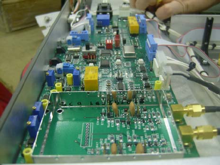
The MXi amplifier control board (Assembly 31C1897) is a single-circuit assembly that provides all of the amplifier
control functions required for the MXi series of transmitters on a single circuit board. This board can be configured
for a number of different transmitter types, power levels, transmission standards and options.
Figure 1 MXi Controller
The board implements controls/status/telemetries for remote control through a rear panel connector that will
interface to a typical remote control system (such as Moseley or Gentner), when used in an MXi802 or MXi1002
the controls are disabled. An RS232 serial port is also provided to allow the operator to communicate with the
main controller located inside the power supply chassis. The MXi control board has RF detectors for forward and
reflected power and all the circuitry to support AGC/VSWR/Cutback functions.
The MXi board has a BDM (Background Debug Mode) connector that allows an external computer or laptop to
download the software program into the CPU chip. The CPU chip holds the program in its internal Flash memory
and so there is no external chip or device that need be replaced to change/upgrade the software.
The concept of this design places all of the control and monitoring functions in one place and therefore eases the
setup and maintenance functions on this series of transmitters.
PUB11-017 Rev 1 Dec 8, 2011 11-017-1 Amplifier Controller Board Rev.3
AMPLIFIER CONTROLLER BOARD REV.3
2
2.1
2.1.1
2.1.2
2.1.3
2.1.4
2.1.5
2.1.6
GENERAL OPERATIONS
CONNECTOR AND SIGNAL DEFINITIONS
The connectors on the MXi control board are all shown in Figure 9, which is sheet #3 of the Schematic. The
individual signals that are associated with each pin of the connector are also given. A brief description of each of
the connectors on the board follows.
J1 BDM (Background Debug Mode) Connection
This is used by the software developer to debug the software programmed into the HC08 CPU.
The software program is also downloaded into the HC08 CPU via this connector.
The operator has no real use for this connector since it requires a special interface board.
J2 Remote RS232 Connection
This connector would normally have a nine-pin ribbon cable attached to route the serial signals to the rear panel
nine-pin D-shell connector. Although J2 has 10 pins, only the first nine are actually used with pin 10 being left
open. A typical three-wire serial port (TxD, RxD and Ground) is implemented on this connector to allow interface
to an external laptop or PC. When used in an MXi802 this connection is used to communicate with the main
controller located inside the power supply chassis.
J3 Front Panel LCD and Touchpad
This uses a ten-wire ribbon cable to send and receive serial data from the Front Panel LCD/Touchpad assembly.
This connection is a typical three-wire serial port (TxD, RxD and Ground) that communicates with the
LCD/Touchpad.
For an MXi802 and MXi1002 this connection is not used; the touchscreen is located in the power supply chassis.
J4 +50 Volt DC Power Supply
This is a two-pin connector used for the +50VDC power that is supplied to the RF amplifier. The +50V source is
fed into one pin, run through a current sensor on the MXi board and then fed back out the second pin to the RF
Amplifier. This is the manner in which the current that the +50V power supply is measured. The voltage telemetry
sample from the +50V power is also taken from this connector. When an internal power supply without its own
current metering is being used, this connector is functional.
For an MXi802 and MXi1002 this connection is not used; current metering is done in the power supply chassis.
J5 +50 Volt DC Power Supply Sensing (External)
This uses a six-pin connector that has all the interface connections for the +50V power supply. Included is an ON
command, P/S OK status and a ground reference from the power supply. In the case where an external power
supply is being used with its own current metering, the +50V sample and the current telemetry is fed into this
connector.
The last signal on this connector is a +12V power supply input that is used to power the MXi amplifier controller
board itself. The ground reference is shared with that of the +50V power supply.
J6 Remote Interface
This uses a 15-wire ribbon cable to send status/telemetry and receive commands from the rear panel 15-pin D-
shell connector. Although J6 has 16 pins, only the first fifteen are actually used with pin 16 being left open. In
addition to the remote signals, there is a single set of contacts made available as an external interlock. This can
connect to an external device or be used as a simple remote ON/OFF. When this board is used in an MXi802 or
MXi1002 the controls are disabled but the status and telemetries are still available.
PUB11-017 Rev 1 Dec 8, 2011 11-017-2 Amplifier Controller Board Rev.3
AMPLIFIER CONTROLLER BOARD REV.3
2.1.7
2.1.8
2.1.9
2.1.10
2.1.11
2.1.12
2.1.13
2.1.14
2.2
2.2.1
J7 Transmitter Switch Interface
This uses a nine-wire ribbon cable to send status/telemetry and receive commands from the rear panel nine-pin
D-shell connector. Although J7 has 10 pins, only the first nine are actually used with pin 10 being left open. This
ribbon cable may not be installed if there is only a single transmitter system or if there is no transmitter switching
unit included in the RF system.
J8 Fan Interface
This uses a special connector mounted on the bottom of the MXi amplifier controller board to connect to the fan
assembly. The fan assembly normally includes up to four fans that are mounted below the MXi amplifier controller
board and is inserted from the bottom of the transmitter control chassis. This connector has ON/POWER control
for each of the fans along with a ground reference and a rotational status signal that comes from each of the fans.
J9 External Controls
This has a seven-pin connector that is used to input a variety of signals into the MXi amplifier controller. A pair of
pins are used for the External interlock that is connected to a terminal block on the rear chassis (this is in parallel
with the external interlock on the Remote Controls J6). There is also a thermal interlock that is sent from the RF
amplifier. A remote control VOR (Video Operated Relay) input (RC_VOR) is made available which is in parallel
with the RC_VOR control input of the Remote Controls J6.
J10 AGC Control
This is a three-pin connector that sends a DC reference voltage (with ground reference and shield) to the RF
preamplifier module. This DC reference is generated by the AGC circuitry on the MXi amplifier controller to control
the RF output level of the amplifier.
J11 Aural Detector (Optional)
This is an 11-pin connector that allows the option aural RF detector to be mounted above the normal RF
detectors. This connector is located in the shielded box on the left side of the MXi amplifier controller board and is
not normally visible if the cover is installed on the shield box.
J12 Forward RF Sample
This SMA connector receives the forward power sample from the directional coupler mounted at the rear of the
heatsink. This is used by the RF detector to monitor the level of the RF forward power.
J13 Reflected RF Sample
This SMA connector receives the reflected power sample from the directional coupler built mounted at the rear of
the heatsink. This is used by the RF detector to monitor the level of the RF reflected power.
J14 Front Panel LCD Power
This is a two-pin connector that sends power (+5V and ground) to the Front Panel LCD/Touchpad assembly.
For an MXi802 and MXi1002 this connection is not used; the touchscreen is located in the power supply chassis.
JUMPER OPTIONS
BDM Slide Switch S2
This two pole switch is used to allow the programming of the microprocessor memory with an external
programmer. It is not normally required by the field personnel unless an upgrade of the internal software is
required. This switch should be in the "NORM" position which is away from the top of the board.
PUB11-017 Rev 1 Dec 8, 2011 11-017-3 Amplifier Controller Board Rev.3
AMPLIFIER CONTROLLER BOARD REV.3
2.2.1.1. Dip Switch S3 System Configuration
These DIP switches are reserved for factory test and system configuration. At the time of publication, they are not
assigned for specific functions. When loading the program code into the HC08 micro, these two dip switches
must be in the closed position.
2.2.1.2. Jumper E1–Debug/Normal Mode
This jumper allows factory programming and debug of the HC08 microcontroller. This should always be in the
Normal position for proper operation in the field.
2.2.1.3. Jumper E2–Remote Control Reset
This jumper allows the operator to use the remote Reset command to effect a reset of the HC08 microcontroller.
This would only be installed if there were a suspicion that the microprocessor is hanging-up and the operator
would intend to reset it remotely. This is purely for diagnostic purposes only and should not normally be
permanently installed.
2.2.1.4. Jumper E3–Spare Line Configuration
This jumper allows the signal into the PA0 pin 32 of the HC08 microcontroller to be configured as either an input
or output. This configuration would already have been done in the software at the factory and this jumper setting
should not be altered in the field unless directed by LARCAN personnel.
2.2.1.5. Jumper E4–External or Internal Power Supply Current Sensing
The MXi Amplifier can be configured with a +50VDC power supply that has a built-in current sensing telemetry or,
when the power supply lacks this facility, the MXi controller can measure the current from the +50VDC supply
using the onboard current sensor. When the power supply has its own current sensing telemetry, jumper E4
would be set to the External position. When the power supply does not have its own current sensing telemetry,
jumper E4 would be set to the Internal position allowing the controller’s own current sensor to provide the
telemetry.
In this configuration he amplifier uses external power supplies that have their own current sensing and therefore
this jumper would be set in the "Ext" position. This jumper is normally set at the factory and should not be altered
in the field.
2.2.1.6. Jumper E5–Front Panel ON/OFF Control Switch (System/Manual)
This jumper controls the function of the front panel ON/OFF switch. When in the Ext position, the ON/OFF
command is fed through the HC08 microcontroller allowing the operator to utilize remote ON and OFF
commands. When in the Int position, the ON/OFF directly controls the ON/OFF relay bypassing the
microcontroller and disabling its OFF control ability.
2.2.1.7. Jumper E6–Tx Switching Interlock Enable
Facility has been designed into the controller interlock chain to allow an external interlock contact that a
transmitter switching unit could use to force the amplifier into an OFF state. This would occur if the controller is
moving a coax switch or if this amplifier has been removed from the antenna. When there is no transmitter
switching unit installed, jumper E6 would be installed to disable this particular interlock.
2.2.1.8. Jumper E7–Manual Remote ON/OFF Control
This jumper would be installed to allow the operator to manually turn the amplifier ON or OFF via a remote
command that would directly control the ON/OFF relay and bypass the HC08 microcontroller. For this mode to
work properly, the front panel ON/OFF switch should be left in the OFF position. In normal operation, this jumper
is not installed.
PUB11-017 Rev 1 Dec 8, 2011 11-017-4 Amplifier Controller Board Rev.3
AMPLIFIER CONTROLLER BOARD REV.3
2.2.1.9. Jumper E8–Forward RF Detector, Peak or Average Power
This jumper selects whether the intermediate stage of the RF detector of the Forward power will measure Peak or
Average power. When measuring digital signals, the jumper would normally be set to Average and when
measuring analog signals the jumper would be set to Peak. This jumper determines the amount of RC filtering (or
averaging) of the signal power by selecting which value of resistance is placed in series with capacitor C22. This
jumper is set by the factory depending on the signal standard of the particular amplifier and level that is obtained
from the RF coupler. This should not be changed in the field.
2.2.1.10. Jumper E9–Forward RF Detector Color Burst Trap
When installed, this jumper enables the filter that removes the color burst from the RF signal. This would only be
installed on the analog transmitters, as the digital amplifier does not have a color burst.
2.2.1.11. Jumper E10–Forward RF Detector Sound Carrier Trap
When installed, this jumper enables the filter that removes the sound carrier from the RF signal. This would only
be installed on the analog transmitters, as the digital amplifier does not have a sound carrier.
2.2.1.12. Jumper E11–Forward RF Detector Final Gain Control
This jumper selects either a high or low gain for the final stage of the RF detector of the Forward power. This
jumper is set by the factory depending on the output power of the particular amplifier and level that is obtained
from the RF coupler. This should not be changed in the field.
2.2.1.13. Jumper E12–Reflected RF Detector, Peak or Average Power
This jumper selects whether the intermediate stage of the RF detector of the Reflected power will measure Peak
or Average power. When measuring digital signals, the jumper would normally be set to Average and when
measuring analog signals the jumper would be set to Peak. This jumper determines the amount of RC filtering (or
averaging) of the signal power by selecting which value of resistance is placed in series with capacitor C22. This
jumper is set by the factory depending on the signal standard of the particular amplifier and level that is obtained
from the RF coupler. This should not be changed in the field.
2.2.1.14. Jumper E13–Reflected RF Detector Color Burst Trap
When installed, this jumper enables the filter that removes the color burst from the RF signal. This would only be
installed on the analog transmitters, as the digital amplifier does not have a color burst.
2.2.1.15. Jumper E14–Reflected RF Detector Sound Carrier Trap
When installed, this jumper enables the filter that removes the sound carrier from the RF signal. This would only
be installed on the analog transmitters, as the digital amplifier does not have a sound carrier.
2.2.1.16. Jumper E15–Reflected RF Detector Final Gain Control
This jumper selects either a high or low gain for the final stage of the RF detector of the Reflected power. This
jumper is set by the factory depending on the output power of the particular amplifier and level that is obtained
from the RF coupler. This should not be changed in the field.
2.2.1.17. Jumper E16–AGC Disable Control
When installed, this jumper disables the AGC control of the transmitter and its controller. This is normally only
used with setting up the maximum input drive level for the amplifier. In normal operation, this jumper should
always be removed, since it can allow excessive power to be mistakenly fed through the amplifier.
2.2.1.18. Jumper E17–VSWR Disable Control
When installed, this jumper disables the VSWR trip interlock of the transmitter and its controller. This is normally
only to be used with setting up the VSWR trip level for the amplifier. In normal operation, this jumper should
PUB11-017 Rev 1 Dec 8, 2011 11-017-5 Amplifier Controller Board Rev.3
AMPLIFIER CONTROLLER BOARD REV.3
always be removed, since it removes the VSWR protection from the amplifier. In the presence of a VSWR
condition, this could result in damage to the amplifier FET devices.
2.2.1.19. Jumper E18–Manual VSWR Reset Control
When installed, this jumper allows the operator to directly reset the VSWR trip relay and effectively bypass the
HC08 microcontroller. In normal operation, this jumper would not be installed.
2.2.1.20. Jumper E19– Peak or Sync Detection
This jumper allows the forward power sample to be either a Peak detection or Back Porch detection using the
visual sync. The optional Aural detection piggyback board must be installed to provide the sync detection facility.
For most applications (including all of the digital modulation standards), jumper E19 would be set for peak (Pk)
since there is no vertical sync interval that can be locked onto for these signals. The only application where E19 is
set to the Sync position is when the optional Aural Detection board is installed and Back Porch detection for the
Forward power sample is desired. The purpose of using Back Porch detection is to regulate the output power
more precisely, independent of APL level. This jumper is set by the factory and should not be changed in the field.
2.3 RF DETECTOR OPERATION
The RF Detector circuitry is show in Figure 10. This circuitry can be used for internally diplexed analog
transmitters or for digital transmitters.
RF Power levels are sampled by a directional coupler located on the RF amplifier heatsink and the resulting RF
samples are detected and appropriately processed to provide DC outputs corresponding to the amplitude of the
desired parameter of the input signal. These DC outputs contribute to the AGC/VSWR supervision of the
transmitter and are also processed in analog to digital conversion circuits on the MXi amplifier controller board to
provide digital metering.
The RF Detector can have different group assemblies to support the NTSC system, the PAL system and Digital
transmission. NTSC and PAL application differ only in their color subcarrier frequency, consequently in a few
component values. All group assemblies use the same PC Board and have many jumpers used to change circuit
sensitivity, introduce/remove traps for color subcarrier and/or aural intercarrier and change envelope detector
characteristics for digital and analog applications.
The schematic included in this publication shows the circuitry for NTSC and Digital transmissions. For PAL
systems a separate schematic would be included that is currently not in this publication.
All jumpers are set in the factory and should not be modified in the field unless under direction from LARCAN
personnel.
An optional circuit board is available for internally diplexed analog systems to monitor the aural power separated
from the combined forward signal. This board is mounted on top of the existing RF detector circuitry in a piggy-
back configuration. This extra board uses a sync detector to obtain the back porch (blanking level) of the RF
signal and subtracts the overall RF signal level from the visual only signal level to obtain the aural output. When
this extra board is installed, an added benefit is the provision of a more stable visual output level that is more
independent of APL level due to the fact that the blanking level is used to determine power instead of a simple
envelope detection method. Note that the standard MXi transmitter does not come with this extra board installed
but it must be ordered as an option. When the option is included, an addendum to this manual will be included to
cover this option.
Required signal levels are as follows:
• FWD (overall forward sample) metering requires 20dBm sync peak signal for full scale (100% rated power).
• RFL (overall reflected sample) metering requires 10dBm sync peak signal for full scale (10% rated power).
The forward RF detector can be configured for a number of different signal types as the following table shows.
PUB11-017 Rev 1 Dec 8, 2011 11-017-6 Amplifier Controller Board Rev.3
AMPLIFIER CONTROLLER BOARD REV.3
DESCRIPTION E8 E9 E10 E11
Default Analog NTSC: +20dBm, Visual, Color Burst and Aur Carrier Trapped Pk Installed Installed LO
Default Analog NTSC: +20dBm, Visual, Color Burst and Aur Carrier Trapped Pk Installed Installed LO
Default Analog NTSC: +17dBm, Visual, Color Burst and Aur Carrier Trapped Pk Installed Installed HI
Default Analog NTSC: +17dBm, Visual, Color Burst and Aur Carrier Trapped Pk Installed Installed HI
Special Analog NTSC: +20dBm, Visual+Aural, Color Burst Trapped Pk Installed Absent LO
Special Analog NTSC: +20dBm, Visual+Aural, Color Burst Trapped Pk Installed Absent LO
Special Analog NTSC: +17dBm, Visual+Aural, Color Burst Trapped Pk Installed Absent HI
Special Analog NTSC: +17dBm, Visual+Aural, Color Burst Trapped Pk Installed Absent HI
Digital Signal: +20dBm, Ave Detector, No Traps (also Special Analog NTSC) Av Absent Absent LO
Digital Signal: +20dBm, Ave Detector, No Traps (also Special Analog NTSC) Av Absent Absent LO
Digital Signal: +17dBm, Ave Detector, No Traps (also Special Analog NTSC) Av Absent Absent HI
Digital Signal: +17dBm, Ave Detector, No Traps (also Special Analog NTSC) Av Absent Absent HI
Not Used: Visual + Color Burst and Aur Carrier Trapped X Absent Installed X
Two almost identical detector circuits reside on a single board for visual forward and reflected metering. Detection
sensitivity of the circuit dedicated to reflected visual power is approximately 10dB greater than for the visual
forward RF detector circuit. The reflected port reading is combined visual and aural power. The jumper
configuration for the reflected power follows that of the above table with E12 replacing E8; E13 replacing E9; E14
replacing E10; and E15 replacing E11.
2.4 AGC, VSWR AND CUTBACK OPERATION
The MXi amplifier control board allows for an automatic gain control to maintain the transmitter’s power at a
predefined level. The operator must have first calibrated the RF detector to produce 4.0VDC at the desired 100%
power level of the transmitter. The exciter/modulator must then be set up to produce a drive level sufficient to
allow 110% power with no AGC controls applied. These operations are described in Section 3.
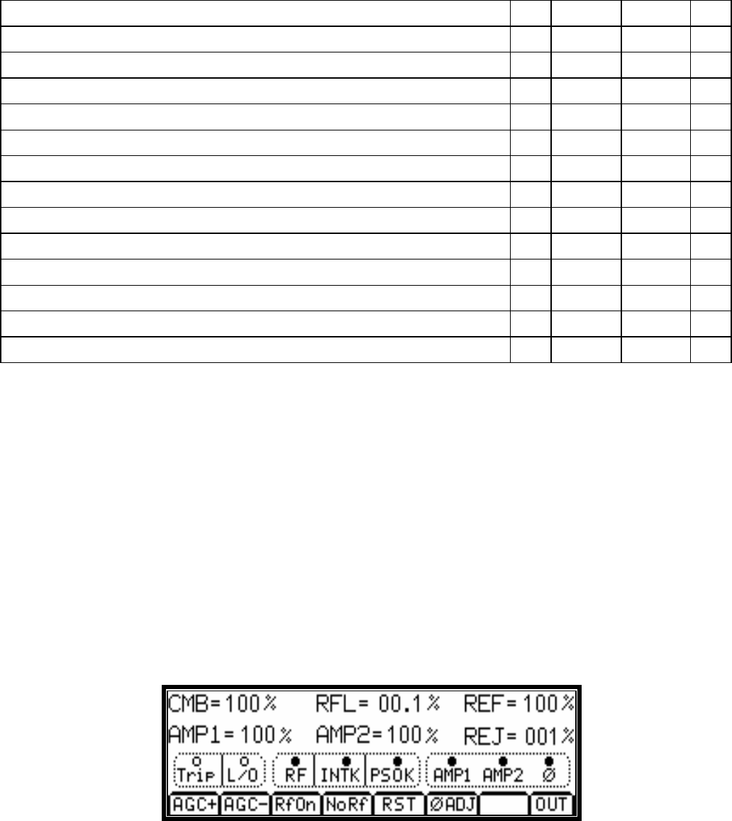
The AGC system generates a desired reference voltage that is set by the operator through the LCD touchpad. To
set the AGC, the operator calls up the Comb submenu from the Main LCD menu. He would then either press the
AGC+ button to increase the power level or the AGC– button to decrease the power level. This sets the reference
voltage for the AGC circuitry. If there is very low RF power, check that the RF status on the third line is lit. If it is
not, then the operator has shut down the RF. Pressing the RF ON menu button restores RF power. The Amps
submenu screen is shown below.
Figure 2 COMB Submenu Screen
The AGC circuit then compares this reference voltage to the actual voltage that is produced from the forward
power RF detector. If there is a difference, this is amplified by a high gain OpAmp and this error voltage is fed out
to connector J10. An external cable connects J10 to the attenuator on the RF preamp mounted on the heatsink.
This will lower the drive to the amplifiers until the transmitter power level agrees with the AGC reference voltage.
PUB11-017 Rev 1 Dec 8, 2011 11-017-7 Amplifier Controller Board Rev.3
AMPLIFIER CONTROLLER BOARD REV.3
Note the AGC voltage from the LCD, if it is near to a value of 0 (i.e., under 0.1V), then there is no AGC action left
and the power cannot be raised any further. If the amplifier power is under 100%, then check the RFL power level
and CUTBACK voltage to verify that the amplifier is not reducing power to protect from a VSWR condition.
The cutback circuit checks the level of reflected power as displayed on the LCD screen above [RFL=00.1%]. If
this reflected power is greater than 1%, the cutback circuit automatically reduces the amplifier forward power to
protect the devices. This indicates a mild VSWR condition such as may be caused by an icy antenna. The
cutback function is a safety protection and is therefore permanently in circuit and cannot (or should not) be
disabled. If the VSWR condition worsens such that reflected power exceeds 10% of forward power, the MXi shuts
the transmitter down.
The MXi has built-in VSWR protection to prevent damage to the amplifier from excessive power being reflected
back from the output system. This VSWR protection becomes operational when reflected power exceeds 10% of
forward power. The system shuts down the amplifier for a few seconds and then tries to restart again. This is
done to check if the VSWR was a temporary condition that could have been caused by a lightning strike nearby.
The LCD shows the TRIP status light on the third row of the LCD to indicate that a VSWR trip had occurred. If the
condition persists such that three VSWR trips occur within 1 minute, the system completely shuts down. The LCD
will then illuminate the L/O (Lockout) status light on the LCD to show that a Lockout has occurred.
2.5
2.5.1
INTERLOCKS
Interlocks on the MXi amplifier can be divided into two different types: hard interlocks that shut down the amplifier
without any CPU intervention and soft interlocks that are generated by the CPU chip in response to abnormal
system parameters.
Hard Interlocks
There are hardware interlocks that directly affect the ON/OFF relay K1 by removing the +12V arming voltage on
its coil and preventing it from turning on. There are four of these interlocks as follows:
2.5.1.1. Amplifier Thermal
Heatsink thermal opens if heatsink temperature is too high. Dry Contact across Connector J9 pins 5 and 6.
2.5.1.2. Transmitter Switching
Interlock provided for an external Transmitter Switching unit to shut down the Transmitter.
Dry Contact across Connector J7 pins 1 and 2.
When there is no transmitter switching, jumper E6 defeats this interlock.
2.5.1.3. External #1
Interlock supplied for customer use such as RF system interlock or RF Load.
Dry Contact across Connector J9 pins 1 and 2.
Parallel contact provided across J6 pins 14 and 15, only one of J6 or J9 is required.
If not used, then this contact should be shorted out externally.
2.5.1.4. VSWR Relay K2
Contact from VSWR Trip relay K2 pins 11 and 13.
Contact will be closed (OK) if there is no VSWR condition.
Contact will open whenever a VSWR is detected.
Note: Jumper E17 disables this interlock, this is for setup only.
PUB11-017 Rev 1 Dec 8, 2011 11-017-8 Amplifier Controller Board Rev.3
AMPLIFIER CONTROLLER BOARD REV.3
2.5.2
2.6
2.6.1
Soft Interlocks
There are parameters that the CPU monitors and if they indicate an error condition, the CPU will issue and OFF
command to the ON/OFF relay and set the appropriate error flag. Note: if the Local or Remote ON/OFF
commands are jumpered to the Override state, the CPU will be unable to shut off the amplifier via K2.
For this reason it is recommended that the ON/OFF controls are left jumpered in the normal positions unless an
emergency condition exists. The software interlock parameters are as follows:
2.5.2.1. Power Supply OK
+50V Power Supply is indicating an error, +12V signal at J5 pin 5 means OK state.
2.5.2.2. Power Supply Voltage
+50V telemetry shows a voltage over +52VDC, Telemetry at J5 pin 6.
2.5.2.3. Power Supply Current
Power Supply Current exceeding the max rating, value depends on MXi model.
For the internal power supply, the telemetry is found at U7 pin 7.
For an external power supply, the telemetry if found at J5 pin 5.
2.5.2.4. Amp Temperature
If the amplifier heatsink is configured with a thermistor. This is optional.
When the heatsink temperature rises too high, the CPU cuts back output power.
This is not a true interlock since the Thermal interlock is used to shut off the transmitter.
This power cutback tries to keep the heatsink from reaching shutoff temperature.
2.5.2.5. Fan Failure
The four fans are monitored for their rotational status.
When one or more fans show a failure, the CPU cuts back output power.
This is not a true interlock, as the Thermal interlock is used to shut off the transmitter.
This power cutback tries to keep the heatsink from reaching shutoff temperature.
EXTERNAL SIGNALS AND REMOTE CONTROL
There are a number of signals that are connected externally at the back panel of the MXi transmitter chassis.
These can be classified as either interlocks, remote controls, external power supplies or transmitter switching.
External #1 Interlock
The interlock that is available on the rear panel is the External #1. This is a single dry contact that is provided to
shut down the RF amplifier in the case of some external problems (such as a bad RF load). It has two possible
connection points that are logically in parallel so that only one needs to be connected. One point is from pins 1
and 2 of J9 on the MXi board. This connector is normally wired to a two-pin terminal block TB1 located on the
back panel. This would be the most accessible and likely connection point.
The second parallel connection is from pins 14 and 15 of J6 on the MXi board which is assigned for Remote
Controls. This 16-pin connector would usually have a 15-wire ribbon cable attached that would route the signals
from the first 15 pins of J6 to a 15-pin D-shell connector on the rear panel.
PUB11-017 Rev 1 Dec 8, 2011 11-017-9 Amplifier Controller Board Rev.3
AMPLIFIER CONTROLLER BOARD REV.3
2.6.2
2.6.3
2.6.4
2.6.5
Remote Interface (Individual)
Connector J6 provides for individual lines of control/status/telemetry that would normally be connected to an
external vendor remote control system (such as Moseley or Gentner). This 16-pin connector would usually have a
15-wire ribbon cable attached that would route the signals from the first 15 pins of J6 to a 15-pin D-shell
connector on the rear panel. The details of the signals on this connector are given in Section 4. For on MXi802
the controls are disabled but the status and telemetries are still active.
Serial Interface
Connector J2 provides a standard three-wire serial interface (TxD, RxD and Ground) that is used for
communicating with the main TX controller located in the power supply chassis. The user could also use this port
to connect to an external computer or laptop serial port. The MXi sends a serial stream out this serial port that
reports all of the operating parameters of the transmitter. It can also receive serial commands from an appropriate
computer program or the main TX controller.
Transmitter Switching Interface
Connector J7 provides for individual lines of control/status/telemetry that would normally be connected to an
external transmitter switching unit. Of course, this switching unit would only be necessary if there are two (or
more) MXi transmitters in the system. For a single transmitter, these signals would not be used. When configured
for transmitter switching, this 10-pin connector would usually have a nine-wire ribbon cable attached that would
route the signals from the first nine pins of J7 to a nine-pin D-shell connector on the rear panel. The transmitter
switch interface consists of a telemetry output of the RF forward power level, a status output indicating TX failure,
and interlock input used to shut down the transmitter and a few spare signals for future use. The exact use and
operation of the transmitter switching unit would be documented in its own publication when implemented.
External DC Power Supply
Higher power MXi transmitters such as the MXi802 and MXi1002 require that the DC power supply for the
amplifier be located external to the amplifier chassis. Connector J5 receives the interface signals for this external
supply. These include a +12V input that provides power to the MXi control board itself, a reference ground, a
sample of the +50VDC that is used to power the amplifier, and current telemetry sample and a control output from
the MXi board used to turn on the supply.
The actual connection is made via a power connector at the rear panel and is wired to connector J5. The actual
connection that supplies the amplifier(s) is wired directly from the rear panel to the amplifier and not through the
MXi control board.
PUB11-017 Rev 1 Dec 8, 2011 11-017-10 Amplifier Controller Board Rev.3
AMPLIFIER CONTROLLER BOARD REV.3
3
3.1
3.1.1
3.1.2
SETUP PROCEDURES
The following sections detail the various set up procedures for the MXi transmitter system. These procedures
should only be done by qualified personnel. If the calibrations and setups are done improperly, it can result in the
transmitter being prone to damage.
The transmitter is normally set up in the factory for the particular operating power required when first installed. Set
up procedures would only be required if certain elements of the MXi transmitter had to be replaced or repaired
that would have affected the calibrations. An example of this would be the MXi amplifier controller board itself, the
output RF couplers, the RF cables or the +50V power supply.
If the output power is being changed, then some setup and calibration would be needed since the transmitter
would be set up for the previous RF power level. Caution: do not increase the power output of the MXi transmitter
beyond the original factory set level without first consulting LARCAN field service.
RF DETECTOR
The RF detector is normally calibrated at the factory or by LARCAN field personnel and should not require onsite
re-adjustments except in the following circumstances.
• The desired output power level of the transmitter is to be changed from the factory setting for a full 100%
power reading. Note that the operator should not just increase and readjust power beyond the
recommended rating of the transmitter without prior approval from LARCAN technical services.
• A replacement MXi amplifier control board or directional coupler has been installed in the transmitter.
This procedure assumes that the RF detector is being set-up with the transmitter connected to an RF modulator
input and output load (or antenna) that is the actual configuration it is intended to operate with.
Test Equipment Required
a) An RF power meter such as the HP 436A or similar. For analog transmitters, a BIRD through-line
wattmeter is sufficient.
b) A Spectrum Analyzer, HP 8558B or similar.
If the operator wishes to set up the unit on the bench, then a number of extra pieces of test equipment are
necessary.
• An RF generator/modulator that will replicate the desired signal and level
• An analog transmitter would need a video generator such as Tektronix 1900 or similar, and a
analog modulator and upconverter
• A digital transmitter would need the Pulse Modulator used with the transmitter.
• RF Load rated at the transmitter power and associated cable
Jumper Installation
If the transmitter is not being upgraded from Analog to Digital service (or vice versa), then there should be no
need to change the jumpers for the traps or gain. If there is a change, the trap jumpers would need to be modified
and perhaps the gain as well.
For Analog service, the color burst and aural carrier traps should normally be installed.
For the forward power sample, this would be jumpers E9 and E10.
For the reflected power sample, this would be jumpers E13 and E14.
For Digital service, the above four jumpers would not be installed.
If the desired transmitter output power is the same as what the transmitter was originally set up for at the factory,
there should be no need to change the gain jumpers on the RF detectors.
PUB11-017 Rev 1 Dec 8, 2011 11-017-11 Amplifier Controller Board Rev.3
AMPLIFIER CONTROLLER BOARD REV.3
If a change in power is required or the directional coupler has been changed or the transmitter is being moved
between Analog/Digital service, the RF detector should be first set to the lowest possible gain and the jumpers
moved to increase the gain.
For the forward power sample, the gain is controlled by jumpers E8 and E11.
Digital + Low Gain: E8= Av and E11=LO
Digital + High Gain: E8= Av and E11=HI
Analog + Low Gain: E8= Pk and E11=LO
Analog + High Gain: E8= Pk and E11=HI
For the reflected power sample, the gain works identically where E12 is the same as E8 and E15 is the same as
E11.
3.1.3
3.1.4
3.2
Verify OpAmp Offsets
1. With no RF signal applied, measure the voltage at TP1 and adjust R58 to make this level under 0.1VDC
2. With no RF signal applied, measure the voltage at TP4 and adjust R80 to make this level under 0.1VDC
Verify Output Power Level
1. Attach the RF output power measuring device (Wattmeter or Average Power Meter) to the RF output.
2. Turn down the drive level of the modulator/upconverter before applying the RF input signal.
3. Turn up the drive level until the output power measures the desired reading. Do not use the meter of the
transmitter itself to determine output power, since at this point it may be uncalibrated.
4. When increasing the power, it is always instructive to measure the current on the 32VDC supply in case
there is a problem with how the output power meter is connected or working. If the supply current is
increasing but the output power is not, set the drive to a sufficiently lower level and double check your
setup.
5. When the RF output power is at the desired level, do the following checks:
a) For the forward power sample, the voltage at TP1 should be within 4.5 to 9.0VDC as a maximum
b) If not, then you have either too much power or too high a coupling in the directional coupler.
6. Reverify the output power: if this is correct, a pad can be inserted between the coupler and J12.
7. Adjust potentiometer R48 until the voltage at TP3 is 4.0VDC.
8. To calibrate the reflected power, install jumper E17 that prevents any VSWR trips
9. Remove the RF cable from J12 and attach a –10dB pad, then connect this reduced forward power
sample to J13.
10. If the original power sample into J12 required a pad, this must be retained in addition to the –10dB pad.
11. For the reflected power sample, the voltage at TP4 should be within 4.5 to 9.0VDC as a maximum
12. If not, reverify that the output power has not changed in the meantime.
13. Adjust potentiometer R80 until the voltage at TP5 is 4.0VDC.
Note: Make sure that you remove jumper E17 when done, else you will have no VSWR protection!
At this point, the operator should proceed to verify cutback and VSWR trip functions, as described in the next two
sections.
CUTBACK PROTECTION
Before the operator attempts to set up the cutback circuitry, the forward and reflected power levels must be
properly set up to calibrated levels as described in Section 3.1.
PUB11-017 Rev 1 Dec 8, 2011 11-017-12 Amplifier Controller Board Rev.3
AMPLIFIER CONTROLLER BOARD REV.3
To set up the cutback level, a power sample must be fed into the reflected power connector of the MXi board that
is –16dB down from the forward power sample level. The most convenient way to accomplish this is to take this
sample from the RF monitor port on the rear of the transmitter chassis.
1. Disconnect the AGC control connector J10 from the MXi board to remove any possible AGC or cutback
action while verifying the Reflected power. If the forward power is greater than 100%, adjust the output
level of the upconverter until it is at 100% (+/- 2%).
2. Attach an RF cable from the RF monitor connector at the rear of the MXi control chassis and insert a
–16dB pad. This pad can consist of a –10dB and –6dB pad in series. Remove the RF cable from J13 that
comes from the output coupler and attach a cable from the –16dB pad off the forward monitor sample.
3. We are assuming that the coupling level from the monitor connector is the same as the coupling level for
the forward power RF coupler. To verify this by checking the RFL power level on the LCD, it should read
around 2.5% power. If it is off by more than 0.5%, adjust the amount of padding until the RFL power
reading is within the range of 2% - 3%. A variable attenuator pad would be ideal for this application.
4. Readjust the upconverter output level so that the forward power reads 110% again.
5. Also disconnect the cable from the monitor port for now.
6. Reconnect the AGC control connector J10 on the MXi board.
7. Reconnect the cable from the monitor port to the reflected power sample at J13.
8. Adjust the potentiometer R105 until the forward power reading is about 96% - 98%, which puts the
system just at the edge of cutback.
The setup is now complete, remove the monitor cable from J13 and attach the output coupler back to J13.
3.3 VSWR PROTECTION
The VSWR protection does not really need any setup or calibration since it is fixed to trip when the reflected
power is –10dB of the forward power level. To verify the VSWR trip function, the following steps must be taken.
To check the VSWR trips, a power sample must be fed into the reflected power connector of the MXi board that is
–10dB down from the forward power sample level. The most convenient way to accomplish this is to take this
sample from the RF monitor port on the rear of the transmitter chassis.
1. Disconnect the AGC control connector J10 from the MXi board to remove any possible AGC or cutback
action while verifying the Reflected power. If the forward power is greater than 100%, adjust the output level
of the upconverter until it is at 100% (+/- 2%).
2. Install a jumper in E17 that will prevent any VSWR trips.
3. Attach an RF cable from the RF monitor connector at the rear of the MXi control chassis and insert a
–10dB pad. Remove the RF cable from J13 that comes from the output coupler and attach a cable from
the –16dB pad off the forward monitor sample. We are assuming that the coupling level from the monitor
connector is the same as the coupling level for the forward power RF coupler. To verify this by checking
the RFL power level on the LCD, it should read over 10.1% power but less than 11% power. Note that a
minimum of 10.1% power is needed to insure a VSWR trip. If the RFL power is under 10.1%, decrease
the amount of padding until the RFL power reading is within the range. If the RFL power is too high (over
11%), increase the amount of padding until it is in the range. A variable attenuator pad would be ideal for
this application.
4. Readjust the upconverter output level so that the forward power reads 110% again.
5. Also disconnect the cable from the monitor port for now.
6. Reconnect the AGC control connector J10 on the MXi board.
7. Reconnect the cable from the monitor port to the reflected power sample at J13.
8. Remove the jumper from E17 and the transmitter should trip three times and lock out on the fourth trip.
PUB11-017 Rev 1 Dec 8, 2011 11-017-13 Amplifier Controller Board Rev.3
AMPLIFIER CONTROLLER BOARD REV.3
9. The setup is now complete: remove the monitor cable from J13 and attach the output coupler back to
J13.
10. Clear the VSWR lockout and trip condition by either pressing the front panel reset button or issuing a
remote reset command.
3.4 POWER SUPPLY VOLTAGE AND CURRENT CALIBRATION
To set up the power supply voltage and current reading, the operator must view the readings on the P/S submenu
on LCD display.
1. To set up the voltage reading, turn on the transmitter and verify that the power supply is indeed running.
2. With a voltmeter, measure the voltage on the power supply directly.
3. Adjust potentiometer R14 on the MXi amplifier control board until the displayed voltage equals that being
measure by the voltmeter.
4. To set up the current reading, the power supply should be ON as in the above paragraph and enough RF
drive (at least 50%) should be applied to get a reasonable current level for calibration.
5. With a clamp on Ampmeter, measure the current on the main feed coming from the power supply.
6. Adjust potentiometer R15 until the displayed current agrees with that measured on the clamp on meter.
If an external power supply is used that has its own current telemetry sensing, it may have its own setup as well.
The current reading on the LCD will still be affected by R15 but the external supply may require its own
calibration, if the level it sends to the MXi is too low or high. A good level would be in the range of 2-4 volts for full
scale current.
PUB11-017 Rev 1 Dec 8, 2011 11-017-14 Amplifier Controller Board Rev.3
AMPLIFIER CONTROLLER BOARD REV.3
4
4.1
REMOTE CONTROL CONNECTIONS MXi TRANSMITTER
On the rear of the transmitter Chassis, the remote control connections are available on a 15-pin male D-shell
connector J6. This includes all of the remote controls, status and telemetries available to the operator.
These remote signals are routed from the MXi Control board via a 15-wire ribbon cable from connector J6 of the
MXi Control board. The signals designations for each pin of J6 can be viewed on sheet 3 of the schematic in
Figure 9. The actual circuitry that drives these signals is spread out on all five sheets of the schematic.
When the MXi amplifier controller is used in an MXi802 or MXi1002 the remote controls are disabled but the
telemetries and status are still present.
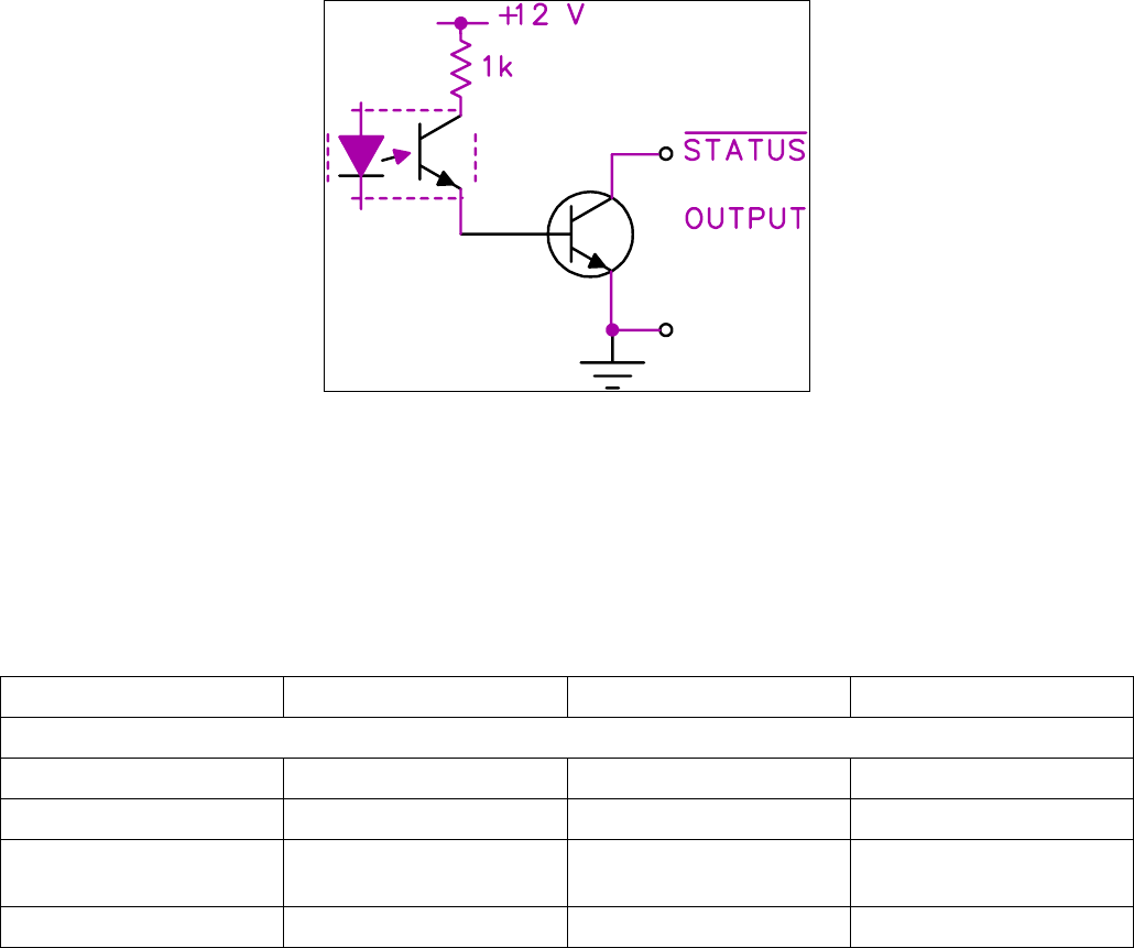
STATUS OUTPUTS
Figure 3 Status Outputs
These are current sinking open collector outputs, out of quad pack MPQ2222 (2N2222A) NPN transistors driven
by opto-isolator devices. The available output sink current is dependent on the gain of the NPN and the opto-
isolator transfer ratio. Generally, one can expect at least 100mA of sinking current for each output listed here.
Because these are open collector, they can be used in special applications, such as on-site warning signal
activation if desired, but they are limited in external circuit voltage to maximum 60VDC. Each status (in
parentheses) indicates what it means when in its active low condition.
The MXi provides three remote control outputs that represent the current operating state of the switching system
via the Digital Output Board
TX D-Connector PC Board Connector Designation Description
Remote Control
Pin 9 J6 Pin 2 RS TXOn Transmitter is turned ON
Pin 2 J6 Pin 3 RS_Error Transmitter has an error
Pin 10 J6 Pin 4 RS_Remote Transmitter is in Remote
Mode
Pin 12 J6 Pin 8 Ground Ground Reference
4.2 TELEMETRY OUTPUTS
These are buffered OpAmp outputs, out of quad pack LM324 operational amplifiers. The available output voltage
is limited to the range of 0 – 5VDC. The OpAmp can reliably source around 5mA of current and so a relatively
high impedance input of at least 2K ohms should be used. Each telemetry has a description to indicate what
parameter it is measuring.
The MXi provides five remote telemetry outputs that represent the current operating levels of the MXi transmitter.
PUB11-017 Rev 1 Dec 8, 2011 11-017-15 Amplifier Controller Board Rev.3
AMPLIFIER CONTROLLER BOARD REV.3
TX D-Connector PC Board Connector Designation Description
Remote Controls
Pin 5 J6 Pin 9 RT_FWD Forward RF power level
Pin 13 J6 Pin 10 RT_RFL Reflected RF power level
Pin 6 J6 Pin 11 RT_AUR Aural RF power level
(optional)
Pin 15 J6 Pin 12 RT_AGC AGC voltage (1/2 scale)
Pin 7 J6 Pin 13 RT_CUTB Cutback voltage (1/2
scale)
Pin 12 J6 Pin 8 Ground Ground Reference
4.3 REMOTE CONTROLS
The Transmitter MODE must be in REMOTE for any of these remote controls to be operational. The transmitter is
placed in the REMOTE mode via the touch LCD menu options as described in Section Error! Reference source
not found.. The main LCD screen has a status light to show if the REMOTE MODE is active.
To place the transmitter into REMOTE MODE, the operator must enter the REMCTL submenu on the LCD and
enable the REMOTE MODE.
The MXi provides 4 remote control inputs that effectively replicate the its own front panel mode control buttons.
The VOR (Video Operated Relay) input is not available from the front panel since it is a special type of input that
only makes sense as a remote input.
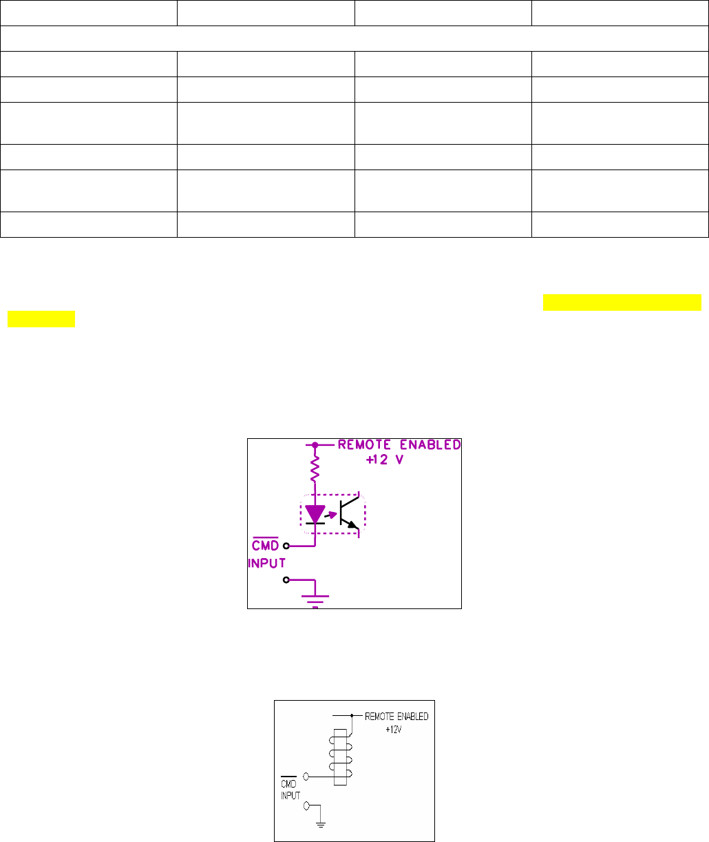
Figure 4 TX_OFF, RESET, and VOR Remote Controls
The TX_OFF , RESET and VOR remote controls are active low, opto-isolated inputs configured as shown, all of
which require a GROUND for assertion and the activator to be able to sink 15mA or more for at least 200
milliseconds to accomplish reliable keying. Each of these is current-limited by an individual resistor.
Figure 5 TX_ON Remote Control
PUB11-017 Rev 1 Dec 8, 2011 11-017-16 Amplifier Controller Board Rev.3

AMPLIFIER CONTROLLER BOARD REV.3
The TX_ON remote control is an active low input configured to drive a relay coil off +12V supply. It requires a
GROUND for assertion and the activator to be able to sink 100 mA or more for at least 200 milliseconds to
accomplish reliable keying.
TX D-Connector PC Board Connector Designation Description
Remote Control
Pin 1 J6 Pin 1 RC_TX_On Turns Transmitter ON
Pin 9 J6 Pin 2 RC_TX_Off Turns Transmitter OFF
Pin 2 J6 Pin 3 RC_Reset Resets VSWR Trip
Pin 4 J6 Pin 7 RC_VOR VOR On Controls
Pin 12 J6 Pin 8 Ground Ground Reference
Pin 15 J6 Pin 14 EXT1+ Secondary Ext1 Intk
Pin 8 J6 Pin 15 EXT1– Secondary Ext1 Intk
4.3.1
4.3.2
RC_TX_On Remote Transmitter ON Control
The MXi controller has the facility to force the ON/OFF function to follow the front panel ON button. Jumper E5 is
a two-position jumper that can be placed in the EXT or INT position (these are silk screened on the PC board).
When in the INT position and the front panel button is the ON position, this will force the transmitter to the ON
state regardless of the remote or CPU controls. If the front panel button is the OFF position, then the remote ON
command will function normally. When jumper E5 is in the EXT position (normal state), then the remote ON
command will function normally as well.
A second jumper E7 (Manual Control) also affects the remote ON commands. When installed, this jumper
effectively bypasses the CPU and the REMOTE MODE. The transmitter will turn ON whenever there is a low
signal applied to the RC_TX_On command input. When this signal is removed, the transmitter turns OFF. This
jumper is really a Bypass of the CPU’s remote control function and is only meant for emergency purposes. In
normal operation, jumper E7 would not be installed. Also note that if jumper E5 (mentioned above) is in INT and
the front panel ON button is in the ON position, the remote control input will not be able to turn OFF the
transmitter, since it is being held on by the front panel pushbutton.
The following description assumes that jumper E5 is in the EXT position and jumper E7 is not installed.
An active low signal applied to the RC_TX_On command input causes the CPU to read this active state and if the
transmitter is in REMOTE mode, then the CPU will issue an ON command to the ON relay K1.
Note that this changes the transmitter’s state to ON (when in REMOTE) such that after any subsequent power
outage, the MXi transmitter will return to its previous state.
If the operator changes the transmitter’s MODE from REMOTE to LOCAL, the ON/OFF state of the transmitter will
be controlled by the position of the front panel ON/OFF button.
If the operator changes the transmitter’s MODE from LOCAL to REMOTE, the ON/OFF state of the transmitter will
revert to the previous state when REMOTE MODE was active.
RC_TX_Off Remote Transmitter OFF Control
The following description assumes that jumper E5 is in the EXT position and jumper E7 is not installed.
An active low signal applied to the RC_TX_Off command input causes the CPU to read this active state and if the
transmitter is in REMOTE mode, the CPU removes the ON command from the ON relay K1.
Note that this changes the transmitters state to OFF (when in REMOTE) such that after any subsequent power
outage, the MXi transmitter will return to its previous state.
PUB11-017 Rev 1 Dec 8, 2011 11-017-17 Amplifier Controller Board Rev.3
AMPLIFIER CONTROLLER BOARD REV.3
If the operator changes the transmitter’s MODE from REMOTE to LOCAL, the ON/OFF state of the transmitter will
be controlled by the position of the front panel ON/OFF button.
If the operator changes the transmitter’s MODE from LOCAL to REMOTE, the ON/OFF state of the transmitter will
revert to the previous state when REMOTE MODE was active.
4.3.3
4.3.4
4.4
RC_TX_VOR Remote Transmitter VOR Control
The following discussion is assuming that jumper E5 is in the EXT position and jumper E7 is not installed.
The VOR (Video Operated Relay) control is a specialize input that performs a very rudimentary control of a
network of transmitters. The VOR is a signal that is active when video has been present for a specified length of
time, typically around 30 seconds or longer. The presence of video for more than this time causes the CPU to
issue an ON command to the ON relay K1.
When video disappears for more than a shorter amount of time, typically around 5 seconds, the CPU removes the
ON command from the ON relay K1.
This is used when full remote controls are not available for transmitters located in areas that are difficult to
access. In this manner, the operator can turn ON or OFF any number of transmitters in the network by either
applying (or removing) video at the source feed. When this VOR control is being used, the normal remote ON or
OFF commands would not be utilized.
Note that this changes the transmitter’s state to ON (when in REMOTE) such that after any subsequent power
outage, the MXi transmitter returns to its previous state.
If the operator changes the transmitter’s MODE from REMOTE to LOCAL, then the ON/OFF state of the
transmitter will then be controlled by the position of the front panel ON/OFF button.
If the operator changes the transmitter’s MODE from LOCAL to REMOTE, the ON/OFF state of the transmitter will
revert to the previous state when REMOTE MODE was active.
RC_RESET Remote RESET Control
The remote reset command can have four different possible operations depending on which jumpers are selected
in the MXi board.
If both jumpers E18 and E2 are removed (this is the normal mode), the reset command is fed only to the CPU
chip, which then issues a VSWR reset, only if the MXi system is in Remote Mode.
If jumper E18 is installed but E2 is removed, the reset command is manually routed to the VSWR relay reset coil and
effectively bypasses the CPU chip. In this configuration, a remote reset command clears the VSWR relay and does
not depend on the MXi being in Remote Mode.
If jumper E18 is out but E2 is installed, the remote reset command first causes a reset of the CPU chip itself and, if
the MXi system is in Remote Mode, the CPU will itself then issue a VSWR reset command.
If both jumper E18 and E2 are installed, the remote reset command causes a reset of the CPU chip itself and will be
manually routed to the VSWR relay reset coil bypassing the CPU chip.
EXT1 SECONDARY EXTERNAL #1 INTERLOCK
The remote connector also has a pair of contacts that replicate a parallel set of contacts for the EXT1 interlocks at
TB1 on the rear panel. This is not really a remote control, but it could be used as a simple ON/OFF by supplying a
set of controlling contacts across EXT1+ and EXT1–. There is no real polarity required and the + and –
designations are just to differentiate the two pins. The other set of contacts on TB1 should be left unconnected if
this is being used.
PUB11-017 Rev 1 Dec 8, 2011 11-017-18 Amplifier Controller Board Rev.3
AMPLIFIER CONTROLLER BOARD REV.3
5
5.1
CIRCUIT DESCRIPTIONS
MC68HC908 MICROPROCESSOR
The Motorola MC68HC908GT microprocessor (often referred to as the CPU or HC08) performs all of the control
interface and communications in the MXi transmitter system. It is a 44-pin surface mount PLCC type device that is
permanently soldered to the circuit board and is not field serviceable or easily replaced without special surface
mount tooling. A brief description of the part is given in this section and a portion of the manufacturer’s
documentation is given in Appendix A. More detailed information on this part can be obtained from the Motorola
web site.
The HC08 chip used in the MXi can come with either 8K or 16K bytes of non-volatile flash memory, which can be
erased and reprogrammed to allow updating of software code or system parameters. The MXi code is typically
smaller than 8k and so would fit in either size of Flash memory. The HC08 chip has a dedicated serial input pin
designated as the BDM (Background Debug Mode) port that is used to program the internal Flash memory and
for debug testing. The MXi is programmed at the factory and it is not expected that reprogramming would need be
done in the field, although it is possible to do with the proper software. System parameters and status that need to
be retained during power failures (such as the LOG entries) are also stored in the Flash memory.
Most of the external pins on the HC08 are configured as programmable Input/Output (I/O) ports, where the
software program determines whether a certain pin is to be configured as either an input or output. The pins on
the HC08 are grouped together in sets called PORTs. These Ports will have eight pins (or fewer) to support the
byte wide data path in the CPU. Port A is used for general system inputs and outputs. Port B is used as an eight-
channel A/D converter to measure system telemetry values. Port C is used for general system inputs and outputs.
Port D assigns four pins for the synchronous serial port (SPI) with the other four pins used for system inputs. Port
E assigns two pins as a serial communications port (SCI), one pin is the external CPU clock and the other two
pins used for general system inputs and outputs.
The definition of each Port pin is as follows:
PORT A
PA0 Input or Output Jumper E3 configures as I/P or O/P
PA1 Input Remote Control ON Command
PA2 Input Remote Control OFF Command
PA3 Output Select enable for Serial NvPot U16
PA4 Input Front Panel ON Command
PA5 Input Front Panel VSWR RESET Command
PA6 Input 50V Power Supply OK Status
PA7 Input Remote Control VOR Status
PORT B
PB0 Telemetry Temperature of Heatsink [Optional]
PB1 Telemetry Power Supply Current
PB2 Telemetry Power Supply Volts
PB3 Telemetry Cutback Volts [Scaled at half the actual value]
PB4 Telemetry AGC Volts [Scaled at half the actual value]
PB5 Telemetry RF Aural Power [from RF detector - Optional]
PB6 Telemetry RF Reflected Power [from RF detector]
PB7 Telemetry RF Forward Power [from RF detector]
PUB11-017 Rev 1 Dec 8, 2011 11-017-19 Amplifier Controller Board Rev.3
AMPLIFIER CONTROLLER BOARD REV.3
PORT C
PC0 Output Remote Status – Error
PC1 Input DipSw #1
PC2 Input Power Supply (Relay K1) ON Status
PC3 Input DipSw #2
PC4 Input External #1 Interlock
PC5 Output VSWR Reset Control
PC6 Output PS ON Ctl +12V out [could be 24V too]
PORT D
PD0 SPI SS Used by UART
PD1 SPI MISO Used by UART and NvPot
PD2 SPI MOSI Used by UART and NvPot
PD3 SPI SCLK Used by UART and NvPot
PD4 Input Fan#1 Status, Active Low
PD5 Input Fan#2 Status, Active Low
PD6 Input Fan#3 Status, Active Low
PD7 Input Fan#4 Status, Active Low
PORT E
PE0 SCI Transmit Data Used by LCD
PE1 SCI Receive Data Used by LCD
PE2 O/P Remote Status – Remote Mode
PE3 Input VSWR Trip Status
PE4 System Main CPU Clock – 4.9152MHz
The HC08 provides two separate serial interfaces to external components, these are the synchronous peripheral
interface (SPI) and the serial communications interface (SCI).
The SCI implements the standard three-wire serial port (Rx Data, Tx Data and Ground) that would interface to a
typical computer port. The baud is set at 9600. The baud is derived from the system oscillator clock at
4.9152MHz. This frequency is recommended by the manufacturer to easily obtain the most common bauds.
The SPI implements a four-wire clocked serial port that has four signals, Slave Select (SS), Master Out Slave In
(MOSI), Master In Slave Out (MISO) and Serial Clock (SCLK). The HC08 is always set as the Master who
initiates all serial communications. The SPI port is used to communicate with the MAX3110 UART (U2) and the
DS1867 NovPot (U16). The HC08 will send out it data stream from the MOSI line and reads any responses from
the external (Slave) devices via the MISO line. The SCLK is a serial clock (set for around 64K baud) that
synchronizes the data transfer. The presence of this clock allows must higher data rates than the asynchronous
SCI serial protocol. The SS line is a select that enables the MAX 3110 UART when low. A second individual
select line from Port A (pin PA3) is used to select the DS1867 NovPot.
5.2 POWER SUPPLY VOLTAGE AND CURRENT MONITORING
For the following description, refer to Figure 8 (Sheet #2 of the Schematic) in the upper section of the drawing for
the power supply monitoring circuitry. In the case of a MXi802 or MXi1002 the first section describing the on-
board current sensor is for reference only since sensing is done in the power supply chassis.
PUB11-017 Rev 1 Dec 8, 2011 11-017-20 Amplifier Controller Board Rev.3
AMPLIFIER CONTROLLER BOARD REV.3
The MXi board has a built-in Hall Effect current sensor that is able to measure the current drawn by the RF
amplifier from the +50 volt power supply. The standard MXi low power transmitter would have a 25 amp current
sensor. There are two possible sensors that could be installed in the MXi which depend on the actual current level
that is to be measured. A higher power MXi transmitter would be fitted with a 40 amp current sensor. For higher
power transmitters, the power supply would be external to the amplifier chassis and is fitted with its own current
sensor telemetry that is fed into the MXi board separately and the MXi current sensor would be left unused.
Another consideration for making the current sensor external on higher power MXi transmitters is the gauge of
wire required for these higher current make it difficult to wire into the MXi board connector J4.
The circuit board has winding jumpers E20-E23 that allow a single input winding to the current sensor or a dual
winding input to the current sensor. These winding jumpers allow for lower power transmitters (which require
lower power supply currents) to generate a reasonable output voltage from the current sensor. When the winding
jumpers are in the low current setting (“Lo I” = E20 jumpered to E21), this causes the input current to pass
through the input of the current sensor twice (in two windings) producing double the output voltage than would be
generated by a single winding. This is used for lower power transmitters where the maximum power supply
current draw is under half of the rating of the current sensor.
When the winding jumpers are in the high current setting (“Hi I” = E20 jumpered to E22 and E21 jumpered to
E23), this causes the input current to pass through the input of the current sensor only once (in one winding)
producing half the output voltage than would be generated by a double winding. This is used for higher power
transmitters where the maximum power supply current draw is over half of the rating of the current sensor.
When the internal current sensing is being utilized, the MXi expects the +50V to be applied at connector J4 pin 1.
This voltage is passed through a current monitoring circuit and then fed back out on pin 2 of J4 to the RF
amplifiers. The Hall Effect Sensor U9 has a built in voltage reference of 2.5 volts. The sensing output would be at
this 2.5V level when there is no current through the sensor. When current passes through the sensor, then the
output voltage would either increase or decrease from the 2.5V reference. Whether the voltage increases or
decreases depends on the direction of current flow through the sensor thus making this device bi-directional. In
our configuration, the current only flows one way and increasing current will result in decreasing sensor output
voltages. Jumper E4 selects between the internal U9 2.5V reference or an external current sensor. When using
U9 as the sensor, jumper E4 must be placed in the INT position. The output of E4 is fed into the positive input of
OpAmp U7B with the negative input fed from the U9 sensing output such that the OpAmp effectively removes the
2.5V offset introduced by the U9 sensor. A potentiometer R15 is placed in the feedback path of U7A to allow the
current to be calibrated.
When the power supply is external (usual in higher power MXi transmitters), the actual power supply is external to
the amplifier chassis and will then do its own current metering. In this configuration, the MXi board would not have
its own U9 current sensor installed but would receive this telemetry information from J5 pin 5. Jumper E4 selects
between the internal U9 sensing output or an external current sensor. When using the external sensor, jumper E4
must be placed in the EXT position. OpAmp U7A allows for a gain control through potentiometer R15 so that the
current reading can be calibrated.
The Power Supply voltage is expected to be +50 volts DC +/- 0.5V and can be fed into the MXi board from one of
two points, depending on whether the supply is internal or external to the amplifier chassis.
When the power supply is internal to the MXi amplifier chassis, then the MXi expects the +50V to be applied at
connector J4 pin 1. This voltage is passed through a current monitoring circuit and then fed back out on pin 2 of
J4 to the RF amplifiers. This configuration is used when the MXi is a lower power transmitter that can
accommodate the power supply internally.
When the power supply is external (usual in higher power MXi transmitters), the actual power supply is external to
the amplifier chassis and will then do its own current metering. The +50V sample is connected to J5 pin 6 (which
is in parallel with J1 pin 1). Connector J1 is a higher current contact that would allow the current to be passed
through the internal current sensor U9. For an external supply these are not required and so both U9 and J4 will
most likely not be installed on the board.
PUB11-017 Rev 1 Dec 8, 2011 11-017-21 Amplifier Controller Board Rev.3
AMPLIFIER CONTROLLER BOARD REV.3
5.3
5.4
ON/OFF RELAY K1
The ON/OFF relay K1 and associated circuitry is shown in Figure 8. Relay K1 is a four-pole, single-side stable
relay that requires a constant voltage applied to its coil to maintain contact closure. The contacts of this relay
provide the control signals to activate the +50V power supply and the cooling fans.
There are two elements that determine if power is applied to the coil of K1. One is the +12V arming voltage on the
positive side of the coil that comes from the interlock chain. Four interlocks are placed in series with this coil such
that all four must be closed in order for K1 to receive its +12V arming voltage. The four interlocks are Thermal, Tx
Switching, External #1 and VSWR Trip. If any of these interlocks are open, then the relay will not be energized
and transmitter amplifier will be shut down.
The second element that determines if power is applied to the coil of K1 is the control signal on the negative side
of the coil. This control signal can come from one or more of three sources.
The HC08 CPU can always activate the coil from its PC6 pin. This pin activates the base of transistor U10B that
in turn will energize the coil of K1. The second source is the remote control TX_ON command at connector J6 pin
1. When jumper E7 is installed, the remote control TX_ON command can directly energize the coil of K1. The
third source is the front panel ON button. When jumper E5 is in the INT position, the front panel ON button when
pressed in will directly energize the coil of K1. For an MXi802 or MXi1002 the front panel ON button is mounted
in the power supply chassis, not the amplifier chassis and the remote control TX_ON command is disabled.
When K1 is energized, all four poles of the relay will close and cause the transmitter to generate RF power.
Two poles are connected in parallel and send +12V to the fans at connector J8. Two poles are used since the
current rating of one relay pole is not sufficient for the total current draw of up to four fans. One pole is used to
send a +12V command to the +50V power supply. This command causes the power supply to activate and send
its +50V to the RF amplifier. The last pole is used for status, when closed a ground is sent to the remote control
status output RS_TX_ON at J6 pin 5. When K1 is not energized, the ground of this pole is sent back to the HC08
which uses this input to determine if the relay K1 is energized or not.
AGC, CUTBACK AND VSWR
Figure 11 shows the circuitry associated with the AGC, cutback and VSWR functions. Each of these is described
as follows.
The AGC circuit uses the voltage reference that is set by the HC08 CPU via the NvPot U16 pin 13. This voltage is
effectively the desired voltage output that the system wants to see coming from the forward power RF detector.
OpAmp U15A compares the U16 reference voltage to the actual voltage from the RF detector and provides an
error output voltage when the value of the detected voltage is greater than the desired reference. If the detected
voltage is less, then we have lower power than is desired and no AGC action would be needed. The OpAmp 15A
has a high value feedback resistor to provide high gain and cause a strong AGC action for relatively small
changes in output power.
The output error voltage from U15A is fed through a resistor divider that has jumper E16 in the middle of it. If E16
is installed, this shorts out any error voltage from U15A and disables the AGC action. This jumper should not be
normally left installed, it is typically only used during setup operations and should be removed for everyday
operations.
If E16 is not installed, the AGC error voltage is fed to the input of buffer OpAmp U15D and then out the MXi
amplifier control board to the RF PreAmp attenuator via connector J10. The voltage at the PreAmp reduces the
drive level to the RF amplifier and thus reduces the output power.
The AGC error voltage from U15A is divided by two with resistor divider R90/R92 and sent to the inputs of buffer
OpAmps U15B and U15C. U15B provides AGC voltage telemetry for the remote control and U15C provides AGC
voltage telemetry for the HC08 CPU.
The Cutback circuitry monitors the level of reflected power and compares it to a preset level. If the reflected power
exceeds the reference level then an AGC voltage is produces that reduces the transmitter output power. The
purpose for doing this is to protect the Amplifier devices from damage resultant from too much RF power
reflecting back from the output system.
PUB11-017 Rev 1 Dec 8, 2011 11-017-22 Amplifier Controller Board Rev.3
AMPLIFIER CONTROLLER BOARD REV.3
The reflected power sample is sent to OpAmp U17C which compares this with the reference level set by
potentiometer R15; test point TP6. This reference level is set up by sending –16dB of the transmitter forward
power into the reflected port and adjusting R105 until the MXi begins to just start reducing the amplifiers output
power.
When the reflected power exceeds the reference level, OpAmp U17C will generate an error voltage that is fed into
the AGC output OpAmp U15D via diode CR12. This has the same effect as an AGC reduction.
The Cutback voltage from U17C is divided by two with resistor divider R98/R99 and sent to the inputs of buffer
OpAmps U19B and U19A. U19A provides Cutback voltage telemetry for the remote control and U19B provides
Cutback voltage telemetry for the HC08 CPU.
The VSWR trip circuit provides protection to the RF amplifier in the presence of a persistent and high level
reflected power condition. The VSWR system is set to trip at a reflected power level of –10dB down from the
forward power.
OpAmp U17 compares the reflected power voltage with the forward power voltage. When the RF detector setup is
done, the reflected power voltage is set for 4.0V when it is at a level of –10dB lower that the full rated forward
power. The forward power voltage is set for 4.0V when it is at the full rated forward power level. When these two
voltages are equal, then the reflected power is indeed –10dB under the forward power level.
In the case that the forward power sample has been removed or improperly setup, it is possible for the forward
power level to be near 0V or very low. In this condition, any amount of reflected power would cause a VSWR trip
which is undesirable and unnecessary. To prevent this event, OpAmp U17B forces a minimum forward power level
of about 1.5V into U17D that would require a minimum reflected voltage of 1.5V to cause a VSWR trip. This
represents a reflected power level of around –8.5dB instead of –10dB.
When the reflected level exceeds –10dB, set coil of relay K2 is energized, causing a VSWR trip to occur. Relay K2 is
a two-coil latched relay where energizing the set coil causes the contacts of K2 to move into the set position and
remain there even after the coil is de-energized. Once a VSWR trip has occurred, the relay K2 will remain in the set
position until a signal is sent from the HC08 CPU to the other reset coil that moves the contacts back into the original
clear position.
The HC08 CPU can activate the coil from its PC5 pin. This pin forces the output of NAND gate U18A high which
activates the base of transistor U6C that in turn will energize the reset coil of K2.
The VSWR relay has two poles, one for the transmitter interlock and the second for status. The interlock pole is part
of the arming interlock chain of the ON/OFF relay K1. If the K2 contact is opened (i.e., there was a VSWR trip), the
arming voltage is removed from ON/OFF relay K1 and the transmitter shuts down. Note that jumper E17 is provided
to override the VSWR relay trip contacts. This jumper is only for setup purposes and should never be left installed in
normal operations.
Note: Leaving the jumper E17 installed will defeat all the VSWR protection and could result in damage to the RF
amplifier if a high reflected power condition occurs.
The second pole of K2 lights status LED DS10 when the relay has tripped under VSWR condition. The other side of
this pole is fed into the CPU, which uses this to determine if K2 is tripped or not.
5.5 SPI UART
The Maxim MAX3110 is a full single channel serial UART with integral RS232 drivers and receivers. The device
uses the SPI interface to communicate with the HC08 CPU. A brief description of the part is given in this section
and a portion of the manufacturers documentation is given in Addendum 2. More detailed information on this part
can be obtained from the Maxim/Dallas Semiconductor web site.
This device can implement a full serial port with data and handshaking lines. In this application, the handshaking
lines are not used and these inputs/outputs are used for general signal purposes. The RTS output is used as a
remote control TX_FAIL output status and the CTS input is used to read the Thermal Interlock status.
The UART has its own 1.8432MHz crystal to generate the appropriate bauds. The CPU program sets up the baud
as 9600 as the default but this can be altered by user command via the LCD touchpad menus.
PUB11-017 Rev 1 Dec 8, 2011 11-017-23 Amplifier Controller Board Rev.3
AMPLIFIER CONTROLLER BOARD REV.3
An interrupt line is provided by the UART to signal the HC08 CPU when it is available for more data to transmit or
when new data has been received. The device can also interrupt the HC08 in the presence of certain types of
serial transmission error conditions.
The HC08 uses all four of the SPI interface lines to communicate with the UART, since it must both send data to
the UART that must be transmitted and must read data from the UART that has been received. The CPU output
Slave Select (SS) line is used to enable SPI communications with the UART.
The UART has two RS232 drivers and two RS232 receivers that will translate the RS232 level to CMOS/TTL
levels. One driver/receiver pair is used to interface the UART serial data to the LCD when one is present. The
second driver/receiver pair is used to interface the HC08 serial data to the external computer.
5.6
5.7
5.7.1
5.8
SPI NVPOT
The Dallas Semiconductor DS1867 NvPot (non-volatile Potentiometer) dual channel serial potentiometer with
data retention on power down. The device uses the SPI interface to communicate with the HC08 CPU. More
detailed information on this part can be obtained from the Dallas Semiconductor website.
This device implements two independent variable resistances whose value is controlled by data bytes sent by the
HC08 to the NvPot device. These resistances can be varied from close to 0 ohms up to 10k ohms in 256
individual steps (each step would be about 40 ohms each). The NvPot device retains these settings in non-volatile
memory so that they can be restored after a power outage. Figure 7 and Figure 11 show the HC08 CPU and the
NovPot circuitry.
The HC08 only uses two of the SPI interface signals to communicate with the NvPot. The MOSI signal is used to
send data to the NvPot (there is no need to receive any data from the device so MISO is not used).
The SCLK is used to provide the synchronization clock. A separate select line PA3 is used to enable
communications to the device. When PA3 is low, the NvPot communications is disabled and when PA3 is high the
NvPot communications is enabled. The HC08 must co-ordinate the selects between this NvPot and the UART
that share the SPI data line. The select lines are set such that only one of these devices are active at one time.
One of the variable resistance potentiometers is used by the HC08 to set the AGC reference voltage that drives
the AGC circuitry in Figure 11.
The second potentiometer is used to calibrate the thermistor temperature reading from the heatsink. Note that the
thermistor is an optional component and may not be present in all MXi transmitters.
RF DETECTOR
Circuit Description
The board is fitted with two RF detectors, which respond to RF samples fed from RF directional couplers mounted
on output combiner of the Amplifier heatsink. The modulation envelope blanking level is measured because it
remains constant, regardless of the picture content of the transmission. Measurement occurs during the back
porch. Both sections of the board are configured in a similar way.
J12 CHANNEL – VISUAL FORWARD
The RF sample is applied to input J12 and is terminated by R52 in parallel with R53 for an impedance of around
50 ohms. CR5 and Q4 form an envelope detector. CR5 is forward biased slightly by R43 and R54 to overcome
CR5 conduction threshold voltage, thereby improving detection linearity. Q4 is forward biased by R43 as well, and
when RF is applied, Q4 is driven in the direction of turn off during each positive-going half cycle, thus causing its
emitter voltage to become more positive and in effect forming a linear envelope detector.
C24 utilizes the lead inductances of CR5 and Q4 to form a Tee network, which provides a matching section that
improves the UHF signal transfer between the devices. Q4 and CR5 have similar temperature coefficients and the
opposing connection of the two in this back-to-back configuration provides temperature compensation.
Finally, Q4 serves as a low impedance video source. Jumper E9 is used to introduce color subcarrier trap FL1. An
alternate trap consisting of C43, C25 and L1 (marked with asterisks) can also provide this function. The alternate
PUB11-017 Rev 1 Dec 8, 2011 11-017-24 Amplifier Controller Board Rev.3
AMPLIFIER CONTROLLER BOARD REV.3
trap can also be easily changed in values to provide different frequency traps for other systems (like PAL).
Note: only one of either FL1 or the Inductor/Capacitor traps would be installed but never both.
Transistor Q2 serves as a buffer and Q1 serves as another buffer. Following is filter FL2, which removes the aural
carrier. An alternate Inductor/Capacitor trap consisting of L2, C44 and C26 is also provided.
The inverted and amplified video signal is fed to a peak detector comprised of CR4, C22 and R47 through either
resistor R42 (1k ohm) or resistor R46 (33 ohm). Jumper E8 will determine which resistor is in the path and is silk
screened as Pk (peak) or Av (average) on the circuit board. If the RF signal is Digital, then E8 is installed in the
Av position where R42 will effectively form a RC charging circuit that averages the signal and eliminates any
momentary peaks. If the RF signal is analog, then E8 is installed in the Pk position, where R46 will effectively
pass the entire detected envelope to the peak detector.
Because a single supply op-amp is used at U5, the output seen on TP1 and TP2 contains a small DC offset which
must be minimized because low level signals are near ground/earth potential. With no RF input, this offset voltage is
adjusted by potentiometer R58 as near as possible to ground/earth. The setting can be seen when using a DC
coupled scope. Adjust R58 to move the DC level toward ground/earth potential; stop turning the potentiometer
immediately the DC ceases moving. A residual voltage offset of 20 millivolts can be expected for the LM358 family of
op-amps.
The gain of the amplifier stage at U5A can be adjusted by selecting one of the two available feedback resistors R56
(5.1K ohms) or R59 (10K ohms) using jumper E11. When a lower gain is desired, E11 is placed in the LO position
selecting R56 and when a higher gain is desired, E11 is placed in the HI position selecting R59.
The two test points TP1 and TP2 are provided to support the external aural detector. When this option is not
installed, a jumper is placed between J11 pin 5 and J11 pin 6 which placed these two test points at the same
potential.
Outputs from unity gain op-amps U13A, U13B, U13C and U13D drive the forward power metering circuits. The
output of U13A provides telemetry to the CPU A/D converter input. The output of U13B provides telemetry to the
AGC (VSWR) circuitry. The output of U13C provides telemetry to the remote controls and U13D provides telemetry
for the optional transmitter switch connections. Bench test calibration consists of adjusting R48 with rated, properly
modulated input while observing the voltage at TP3, which should read 4.0 volts DC for full scale calibration.
5.9 J13 CHANNEL – REFLECTED
The RF sample is applied to input J13 and is terminated by R74 in parallel with R75 for an impedance of around
50 ohms. CR9 and Q6 form an envelope detector. CR9 is forward biased slightly by R67 and R76 to overcome
CR9 conduction threshold voltage, thereby improving detection linearity. Q6 is forward biased by R67 as well, and
when RF is applied, Q6 is driven in the direction of turn off during each positive-going half cycle, thus causing its
emitter voltage to become more positive and in effect forming a linear envelope detector.
C32 utilizes the lead inductances of CR9 and Q6 to form a Tee network, which provides a matching section that
improves the UHF signal transfer between the devices. Q4 and CR5 have similar temperature coefficients and the
opposing connection of the two in this back-to-back configuration provides temperature compensation.
Finally, Q6 serves as a low impedance video source. Jumper E13 is used to introduce color subcarrier trap FL3.
An alternate trap consisting of C33, C45 and L3 (marked with asterisks) can also provide this function. The
alternate trap can also be easily changed in values to provide different frequency traps for other systems (like
PAL). Note that only one of either FL1 or the Inductor/Capacitor traps would be installed but never both.
Following is filter FL4 which removes the aural carrier. An alternate Inductor/Capacitor trap consisting of L4, C46
and C32 is also provided.
The inverted and amplified video signal is fed to a peak detector comprised of CR8, C30 and R71 through either
resistor R66 (1k ohm) or resistor R70 (33 ohm). Jumper E12 will determine which resistor is in the path and is silk
screened as Pk or Av on the circuit board. If the RF signal is Digital, then E12 is installed in the Av position where
R66 will effectively form a RC charging circuit that averages the signal and eliminates any momentary peaks. If
the RF signal is analog, then E12 is installed in the Pk position where R70 will effectively pass the entire detected
envelope to the peak detector.
PUB11-017 Rev 1 Dec 8, 2011 11-017-25 Amplifier Controller Board Rev.3
AMPLIFIER CONTROLLER BOARD REV.3
PUB11-017 Rev 1 Dec 8, 2011 11-017-26 Amplifier Controller Board Rev.3
5.10
Because a single supply op-amp is used at U14D, the output seen on TP4 will contain a small DC offset which must
be minimized because low level signals are near ground/earth potential. With no RF input, this offset voltage is
adjusted by potentiometer R80 as near as possible to ground/earth. The setting can be seen when using a
DC-coupled scope. Adjust R80 to move the DC level toward ground/earth potential; stop turning the potentiometer
immediately the DC ceases moving. A residual voltage offset of 20 millivolts can be expected for the LM358 family of
op-amps.
The gain of the amplifier stage at U14D can be adjusted by selecting one of the two available feedback resistors
R79 (6.2K ohms) or R82 (20K ohms), using jumper E15. When a lower gain is desired, E15 is placed in the LO
position selecting R79 and when a higher gain is desired, E15 is placed in the HI position selecting R82.
Outputs from unity gain op-amps U14A, U14B and U14D drive the reflected power metering circuits. The output of
U14A provides telemetry to the CPU A/D converter input. The output of U14B provides telemetry to the CUTBACK
and VSWR circuitry. The output of U14C provides telemetry to the remote controls. Bench test calibration consists of
adjusting R72 with rated, properly modulated input while observing the voltage at TP5, which should read 4.0 volts
DC for full scale calibration.
J12 CHANNEL – AURAL FORWARD
Note: This description only applies when the aural metering option has been included in the transmitter system.
The aural metering circuit takes a sample of detected video signal from the forward port and provides DC level
proportional to the amplitude of the aural carrier. The sample of this DC level is used to compensate visual
forward reading affected by presence of the aural carrier at the forward port.
The inverted and amplified video signal is fed to sync separator U9-2. When sync is detected, the sync output at
pin 1 delivers a positive-going composite sync pulse, which turns on Q11 whose collector then goes LOW. If no
sync is detected by U9, its pin 1 remains LOW and Q11 remains off.
After U9-1 pulse has finished, Q11 turns off and its collector output goes HIGH. This LOW to HIGH transition
activates blanking multivibrator U7 and an active low pulse is fed to Q10, turning it on.
Q2, C4, and U2A form a sample-and-hold circuit that samples the signal originating from the emitter of Q1 and which
is buffered by Q18. Sampling occurs during the back porch, and holds during the subsequent horizontal line. This
DC sample is amplified in U2A.
The sample of the signal detected by CR1 from J1 port is buffered by Q3. The wideband visual/aural signal drives
an aural bandpass ceramic filter FL3. The filter is chosen for the broadcast standard in use. C12 couples the
filtered aural CW signal to amplifier Q7. Following is a buffer Q6 and RF amplifier U4. The aural signal from U4
output is then fed to peak detector consisting of CR2, C15, R45. Q8 buffers signal before applying to sample and
hold circuit consisting of Q9, C16 and R52. Sampling aural signal during the back porch provides level
independent of video content.
Because a single supply op-amp is used at U3B, the output seen on TP3 will contain a small DC offset which
must be minimized because low level signals are near ground/earth potential. With no RF input, this offset voltage
is adjusted by potentiometer R34 as near as possible to ground/earth. The setting can be seen when using a DC
coupled scope. Adjust R34 to move the DC level toward ground/earth potential; stop turning the potentiometer
immediately the DC ceases moving. A residual voltage offset of 20 millivolts can be expected for the LM358
family of op-amps.
U3B provides DC amplification of detected signal. Following is another amplifier U5A which gain is set by
potentiometer R59, so DC level at TP4 is in the range of 7VDC. This provides enough “safety” range for the signal
not to saturate or not being high enough for 4VDC calibration at TP5. The sample of aural output is fed to
differential amplifier U3A to compensate for aural carrier influence on visual metering in internally diplexed
systems. R42 is used to minimize this influence. Jumper JPH3 set in position 1-2 enables this compensation,
otherwise JPH3 must be set in position 2-3.
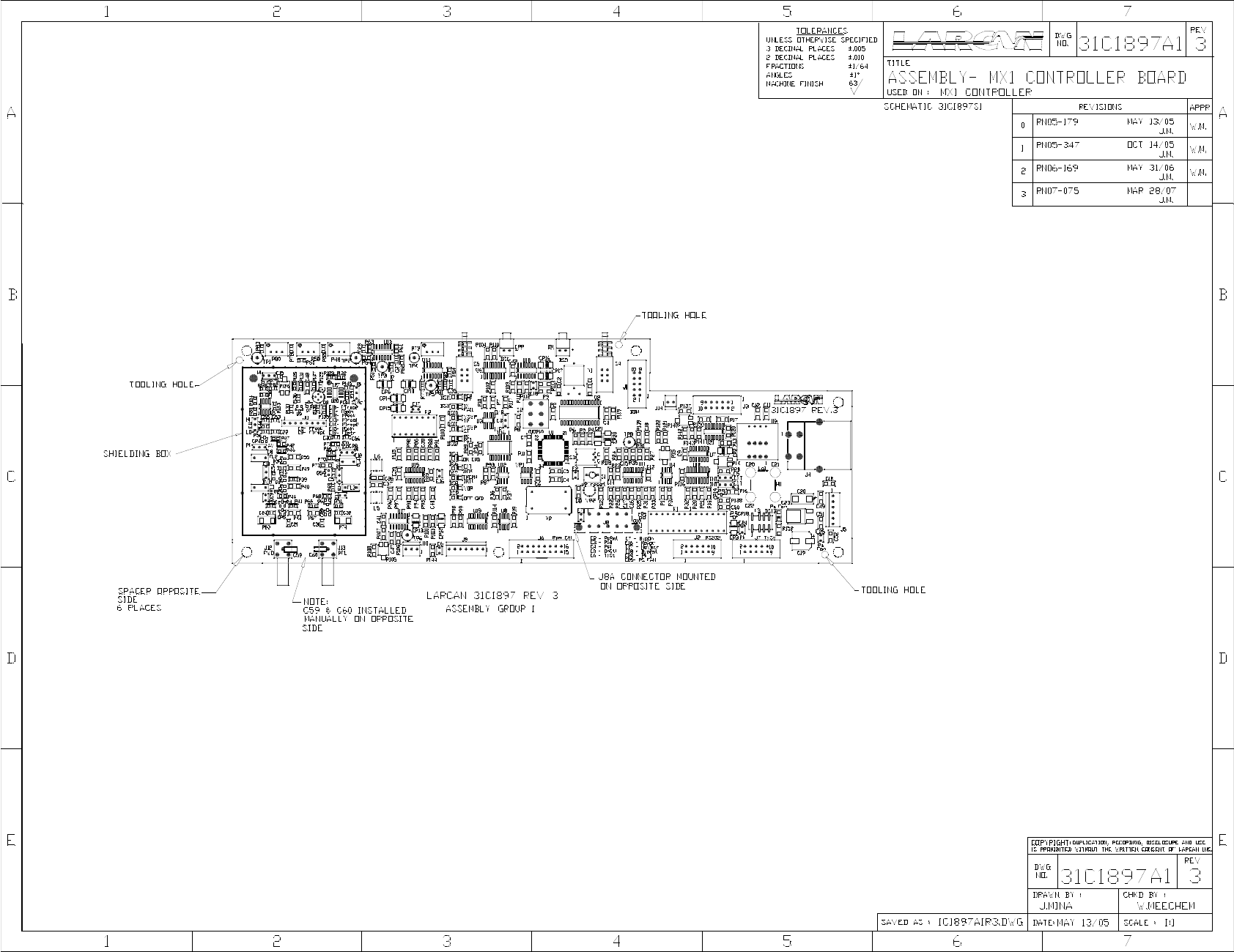
Figure 6 MXi Controller Board Assembly Diagram 31C1897A1
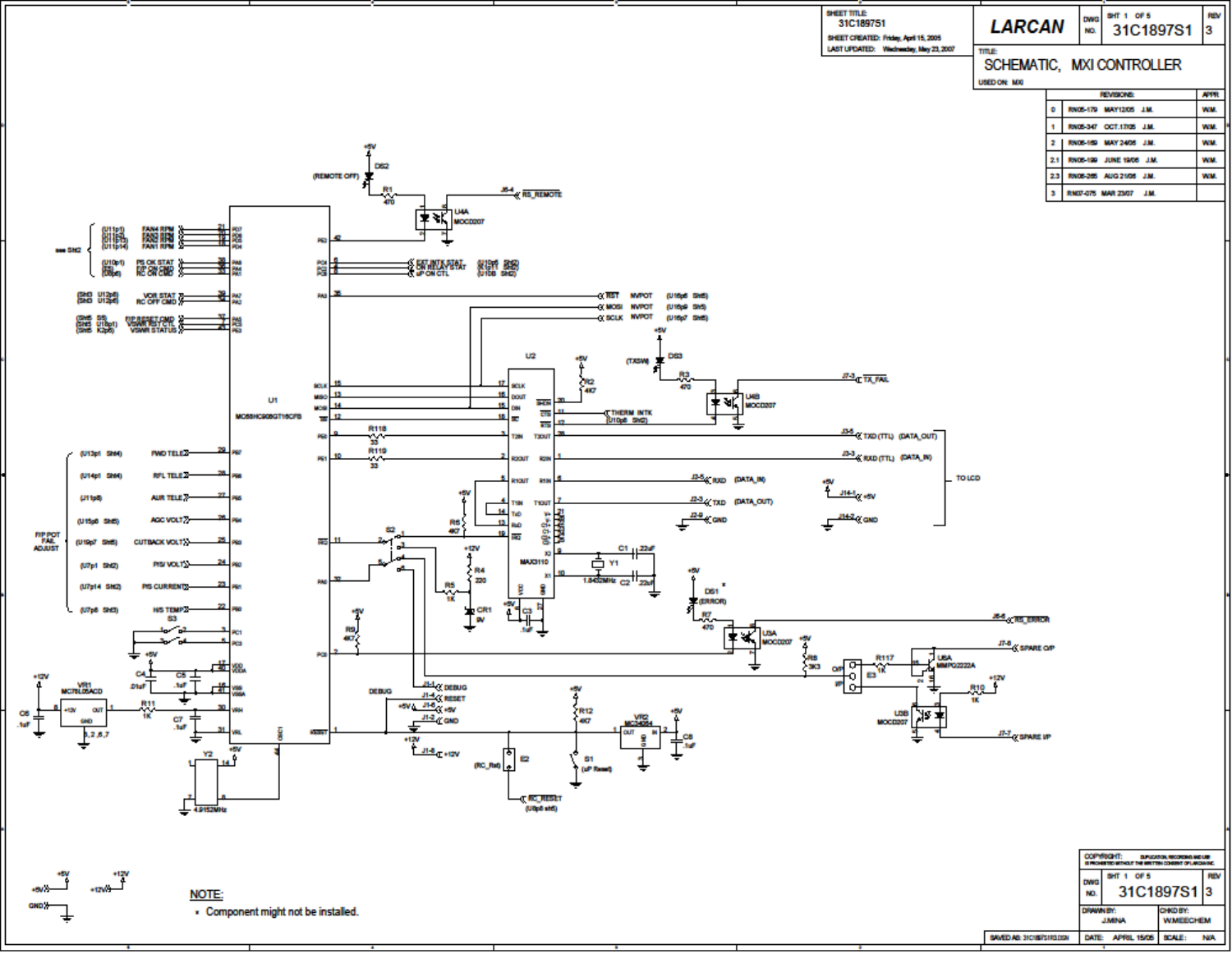
Figure 7 MXi Controller Board Schematic 31C1897S1 sht1
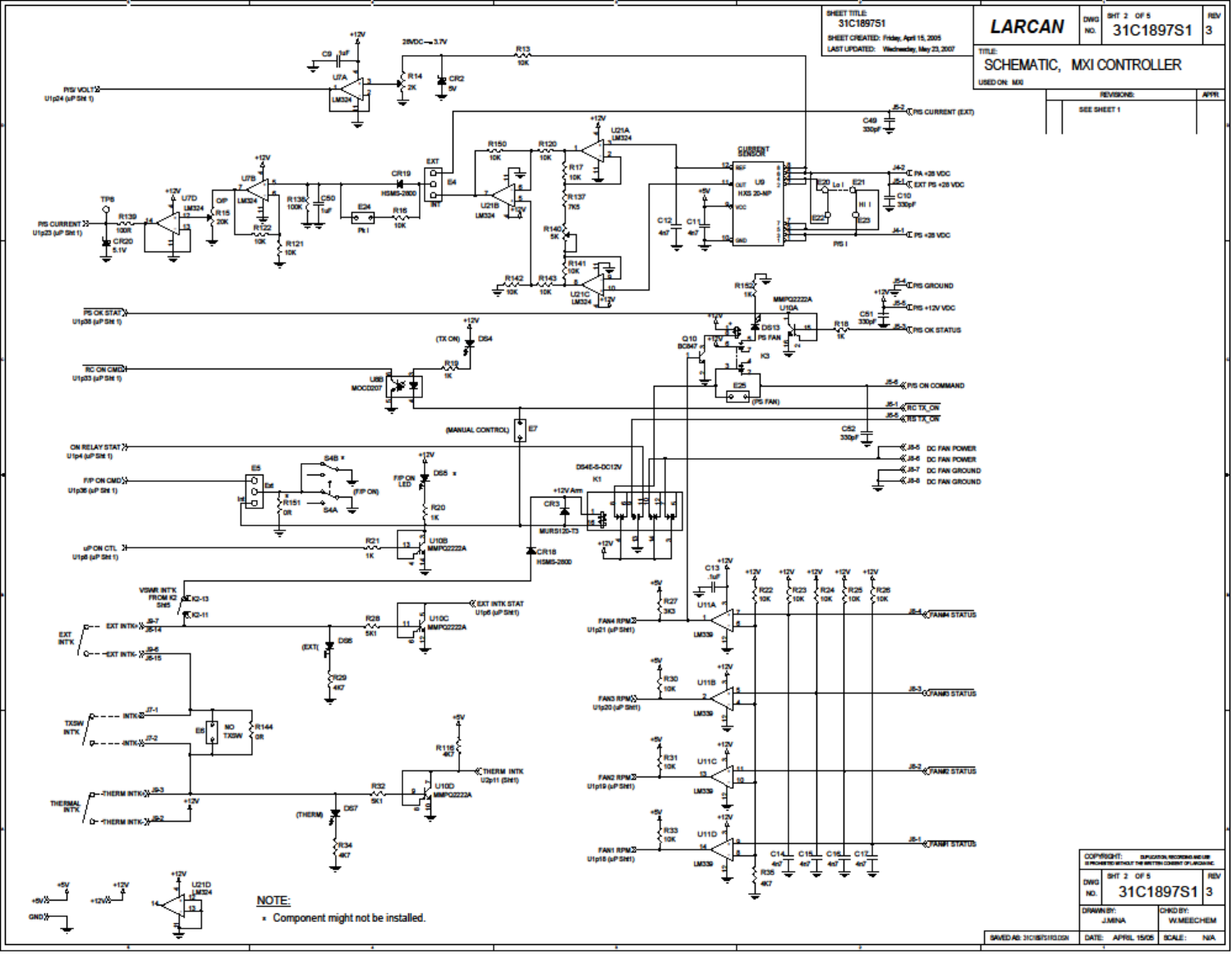
Figure 8 MXi Controller Board Schematic 31C1897S2 sht2
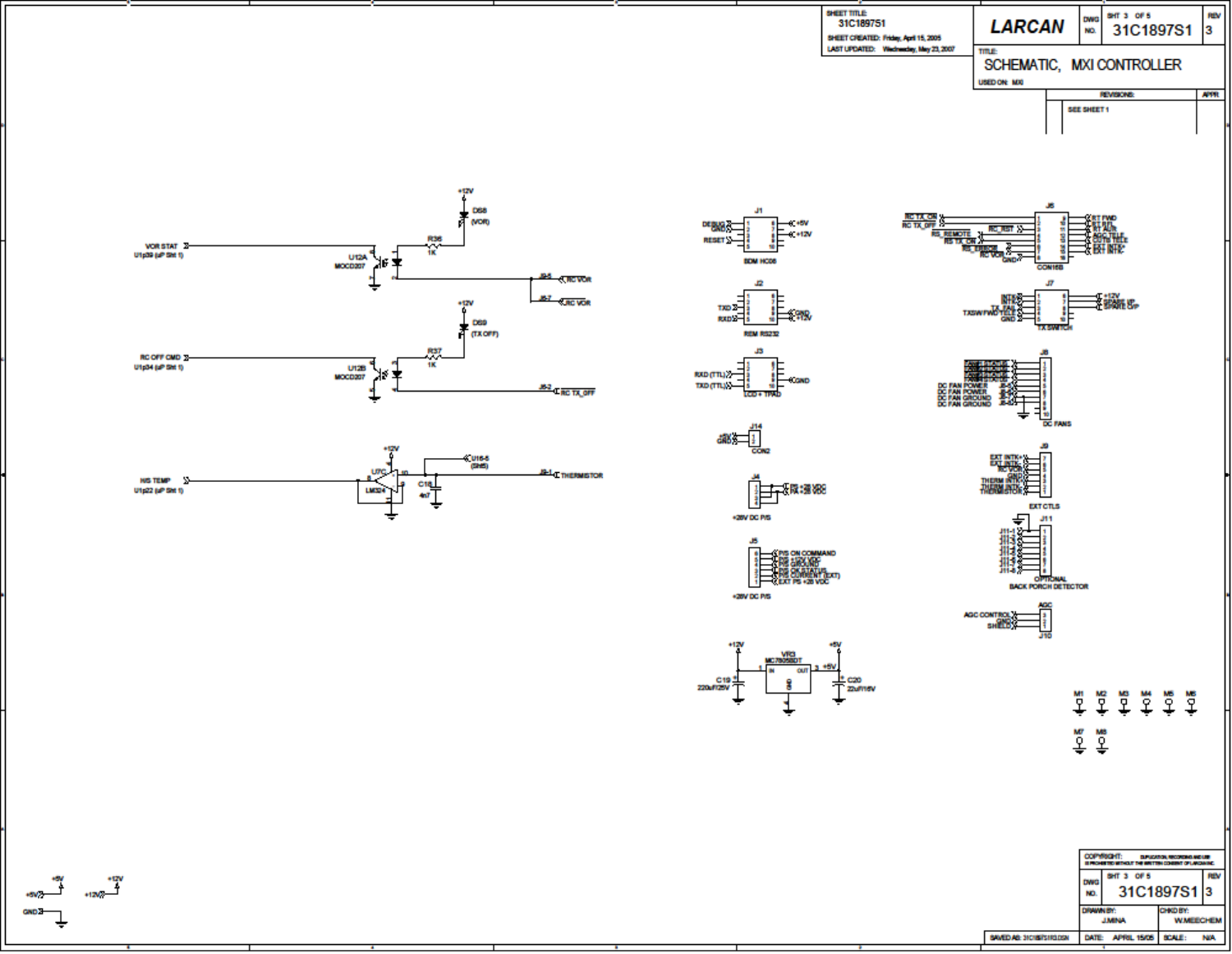
Figure 9 MXi Controller Board Schematic 31C1897S3 sht3
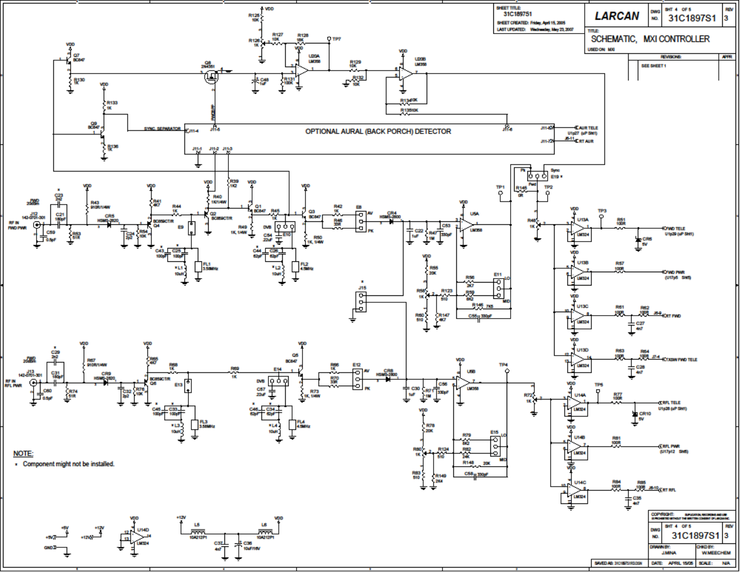
Figure 10 MXi Controller Board Schematic 31C1897S4 sht4
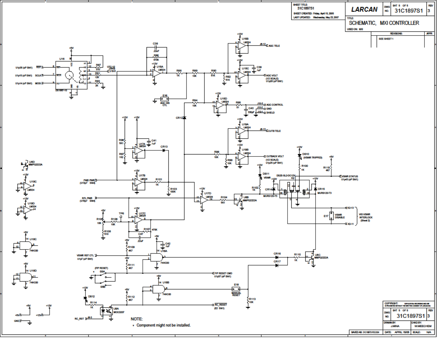
Figure 11 MXi Controller Board Schematic 31C1897S5 sht5

AMPLIFIER CONTROLLER BOARD REV.3
NOTES
PUB11-017 Rev 1 Dec 8, 2011 Amplifier Controller Board Rev.3