Larcan MXI201UD Digital Broadcast Translator User Manual manual
Larcan Inc Digital Broadcast Translator manual
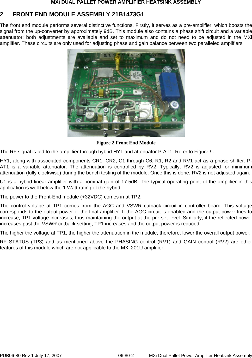
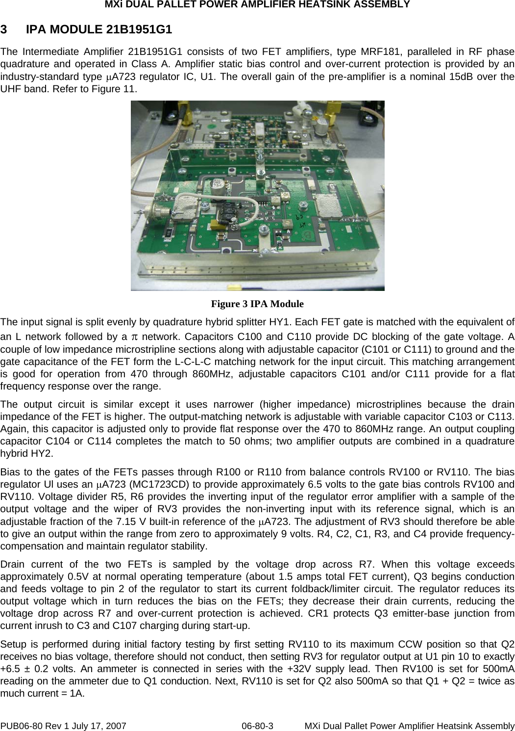
UserManual.wiki
>
Larcan
>
MXI201UD User Manual
manual
Navigation menu
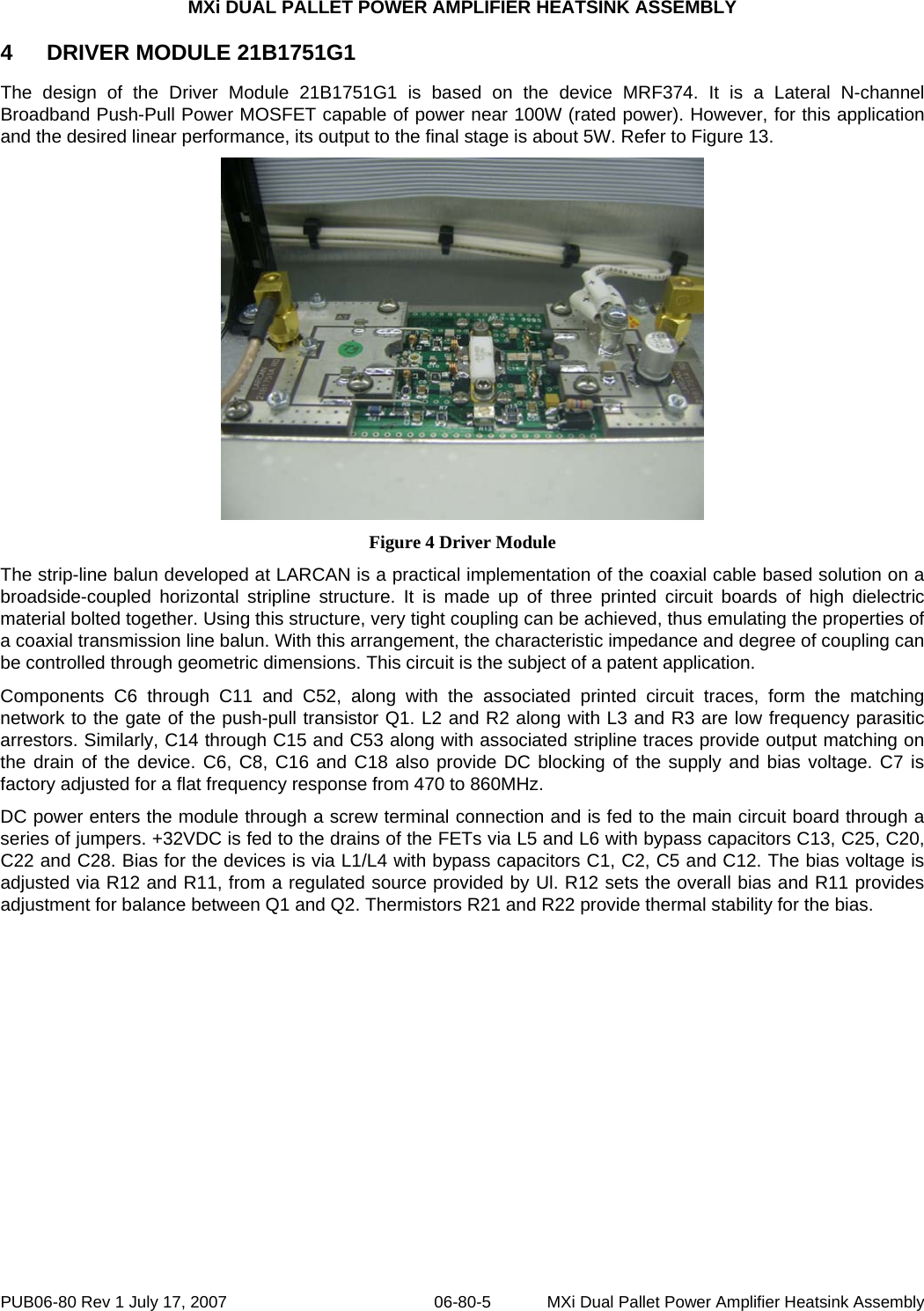
Upload a User Manual
Namespaces
Wiki Guide
HTML
PDF
Info
Views
User Manual
Discussion / Help
Navigation

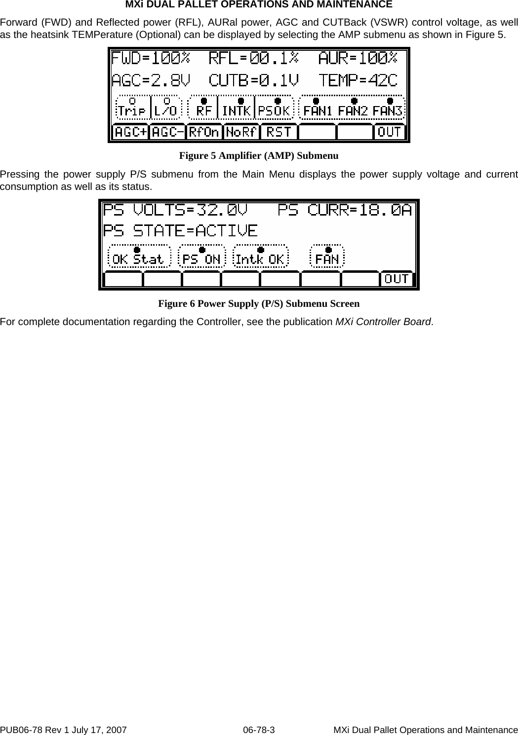

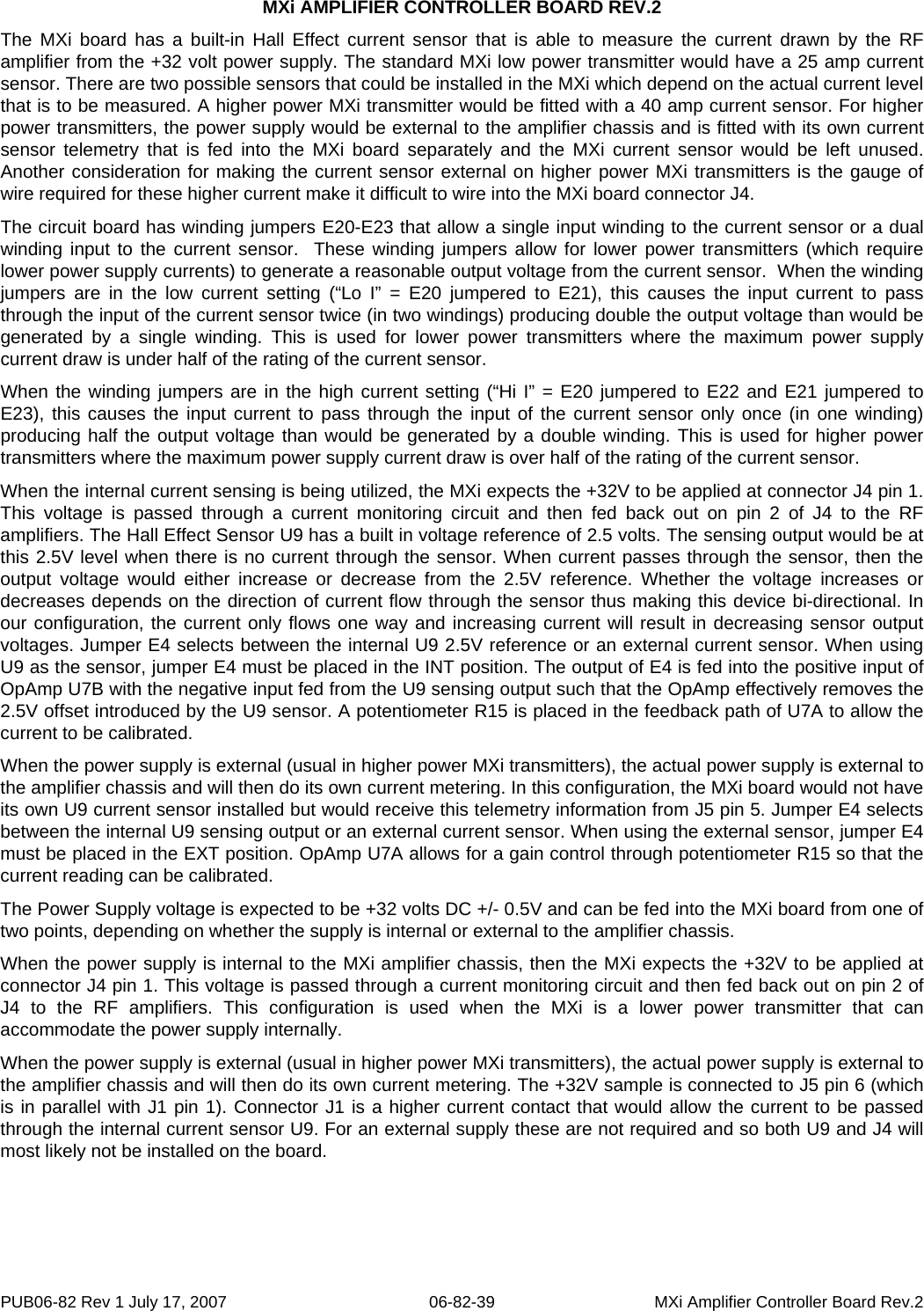
![MXi AMPLIFIER CONTROLLER BOARD REV.2 PUB06-82 Rev 1 July 17, 2007 06-82-10 MXi Amplifier Controller Board Rev.2 Note the AGC voltage from the LCD, if it is near to a value of 0 (i.e., under 0.1V), then there is no AGC action left and the power cannot be raised any further. If the amplifier power is under 100%, then check the RFL power level and CUTBACK voltage to verify that the amplifier is not reducing power to protect from a VSWR condition. The cutback circuit checks the level of reflected power as displayed on the LCD screen above [RFL=00.1%]. If this reflected power is greater than 1%, the cutback circuit automatically reduces the amplifier forward power to protect the devices. This indicates a mild VSWR condition such as may be caused by an icy antenna. The cutback function is a safety protection and is therefore permanently in circuit and cannot (or should not) be disabled. If the VSWR condition worsens such that reflected power exceeds 10% of forward power, the MXi shuts the transmitter down. The MXi has built-in VSWR protection to prevent damage to the amplifier from excessive power being reflected back from the output system. This VSWR protection becomes operational when reflected power exceeds 10% of forward power. The system shuts down the amplifier for a few seconds and then tries to restart again. This is done to check if the VSWR was a temporary condition that could have been caused by a lightning strike nearby. The LCD shows the TRIP status light on the third row of the LCD to indicate that a VSWR trip had occurred. If the condition persists such that three VSWR trips occur within 1 minute, the system completely shuts down. The LCD will then illuminate the L/O (Lockout) status light on the LCD to show that a Lockout has occurred. 2.6 INTERLOCKS Interlocks on the MXi can be divided into two different types: hard interlocks that shut down the transmitter without any CPU intervention and soft interlocks that are generated by the CPU chip in response to abnormal system parameters. 2.6.1 Hard Interlocks There are hardware interlocks that directly affect the ON/OFF relay K1 by removing the +12V arming voltage on its coil and preventing it from turning on. There are four of these interlocks as follows: 2.6.1.1. Amplifier Thermal Heatsink thermal opens if heatsink temperature is too high. Dry Contact across Connector J9 pins 5 and 6. 2.6.1.2. Transmitter Switching Interlock provided for an external Transmitter Switching unit to shut down the Transmitter. Dry Contact across Connector J7 pins 1 and 2. When there is no transmitter switching, jumper E6 defeats this interlock. 2.6.1.3. External #1 Interlock supplied for customer use such as RF system interlock or RF Load. Dry Contact across Connector J9 pins 1 and 2. Parallel contact provided across J6 pins 14 and 15, only one of J6 or J9 is required. If not used, then this contact should be shorted out externally. 2.6.1.4. VSWR Relay K2 Contact from VSWR Trip relay K2 pins 11 and 13. Contact will be closed (OK) if there is no VSWR condition. Contact will open whenever a VSWR is detected. Note: Jumper E17 disables this interlock, this is for setup only.](https://usermanual.wiki/Larcan/MXI201UD/User-Guide-1189565-Page-56.png)
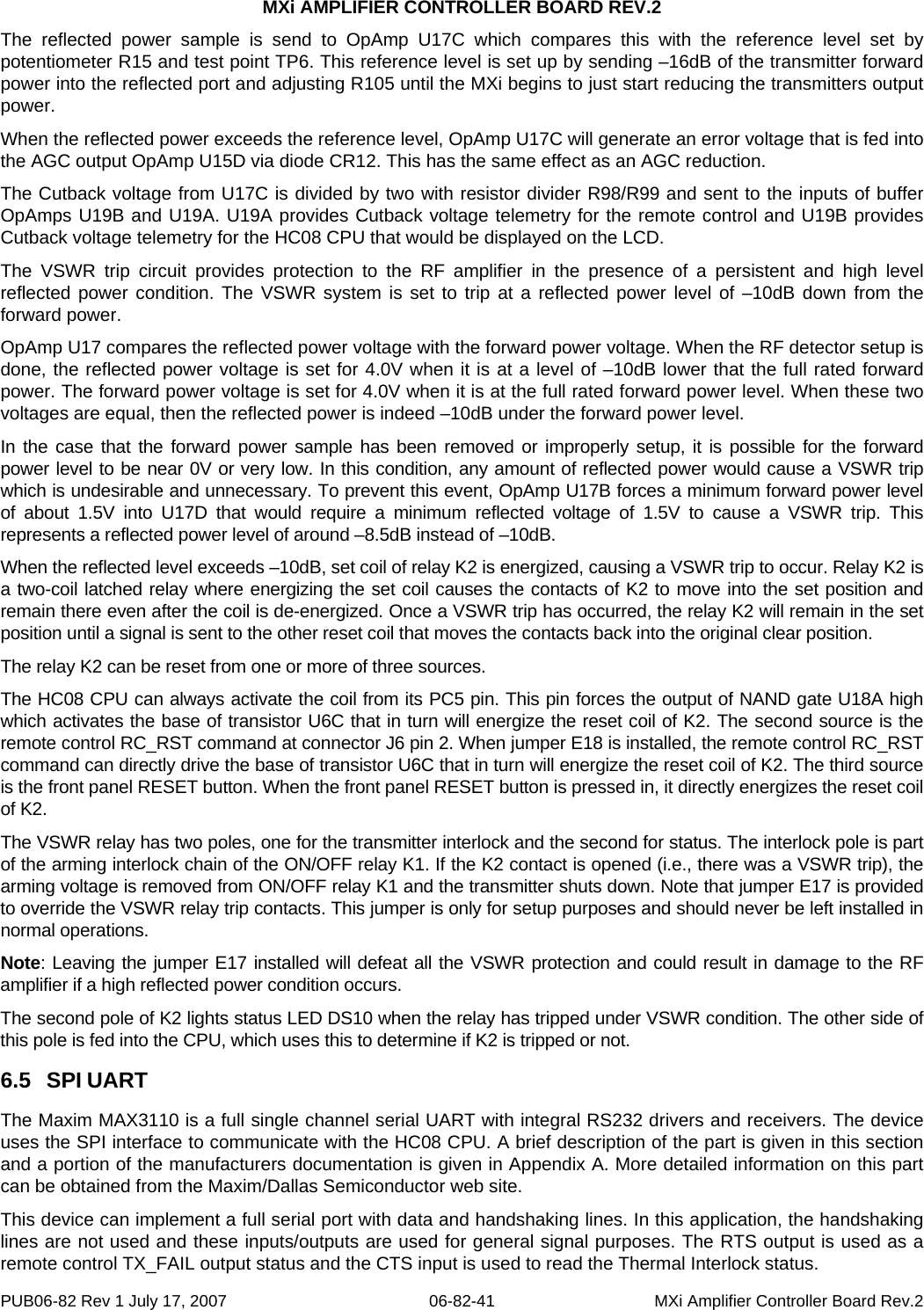
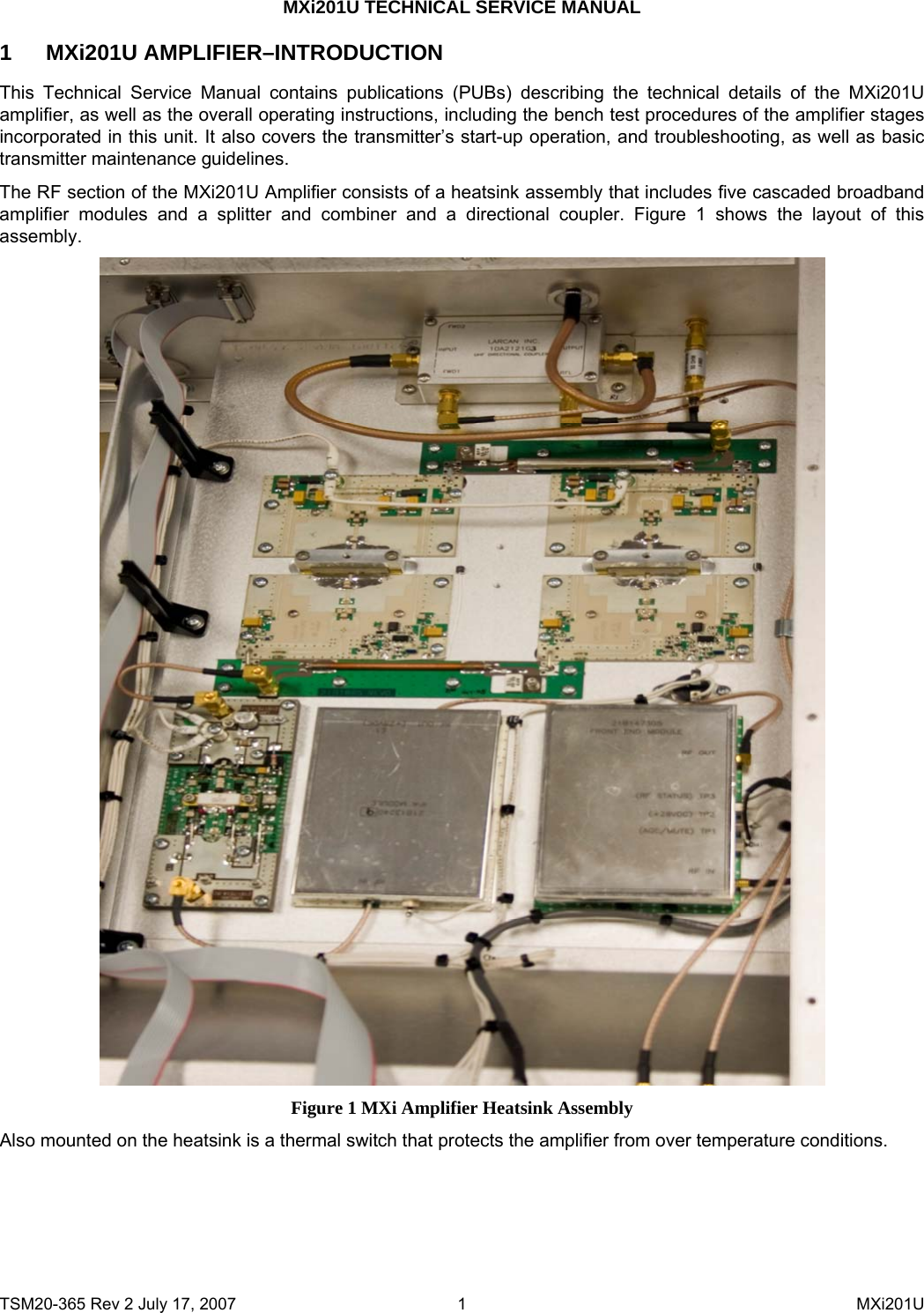
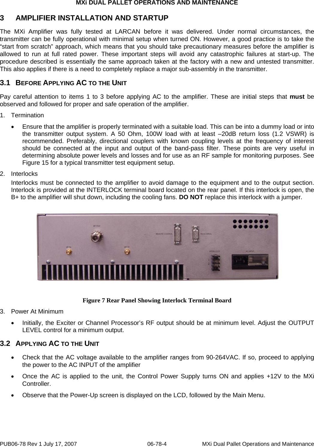
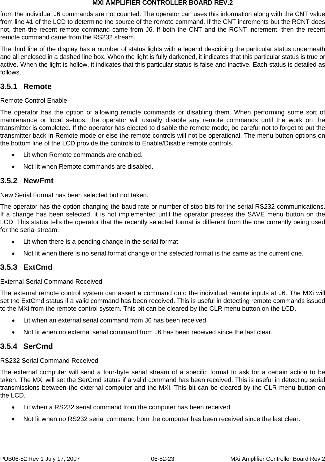
![MXi AMPLIFIER CONTROLLER BOARD REV.2 PUB06-82 Rev 1 July 17, 2007 06-82-13 MXi Amplifier Controller Board Rev.2 3 LCD GUI INTERFACE AND TOUCHPAD The user interface to the transmitter is mainly accomplished with the front panel LCD that incorporates a touchpad as an integral part of the unit. The touchpad consists of a thin membrane attached to the LCD surface which implements a software-driven menu selection system. The LCD has the capability of displaying a number of different screens, which are selected by the operator via the touchpad. Each of the separate display screens (called Menus) are detailed in the following subsections along with their respective touchpad menu options. When the MXi transmitter is first powered on or returns from an AC power outage, the LCD displays a screen [Power Up Screen] that only shows for a few seconds and describes the particular transmitter that this MXi is configured for. The same MXi controller board, LCD and software is used for a number of different transmitter configurations. The one specific Power Up Screen reflects the current transmitter configuration. This same information is available on the General Menu screen described in a later subsection. A sample Power Up screen configured for a 50 watt UHF digital transmitter can be seen below. Note that there are no touchpad menu options on this screen, since it only displays for a few seconds. After these seconds have passed, the MXi proceeds into the Main Menu screen described in the next section. Figure 7 Sample Power-Up Screen 3.1 MAIN SCREEN AND TOUCHPAD OPERATIONS The Main Menu screen as shown below gives the operator all of the most pertinent values and status to verify the operation of the transmitter. This screen is the one that is normally left displayed when no maintenance or diagnostic checks are being performed. It is from this Main screen that all of the other submenu screens can be accessed. If the operator has switched to another submenu, it is recommended that the LCD is returned to the Main screen, since this shows an overview of the system operation. Figure 8 Main Menu Screen The Main screen can be subdivided into four distinct sections, the main forward RF power at the top line, the transmitter status on the second line, the individual subsystem status on the third line and the submenu options on the fourth and last line. The first line shows the forward RF power that the transmitter is currently generating. This is the power that is actually being sent out to the antenna or system load. There are two elements that show the same information but in different formats. The bar graph gives a graphic display of the RF power output level and is calibrated for 100% at the transmitter’s rated output power. The bar graph will display up to 125% but it is not recommended that the operator increase the power beyond the rated power without prior approval from LARCAN field service. When the power exceeds 110%, the bar graph becomes more solid and darker in the area above 110% to indicate that an overpower condition is present. The same information is provided to the left of the bar graph in a three-digit display which shows the current power output. When calibrating or setting up the transmitter, this three-digit display value should be used as a](https://usermanual.wiki/Larcan/MXI201UD/User-Guide-1189565-Page-59.png)
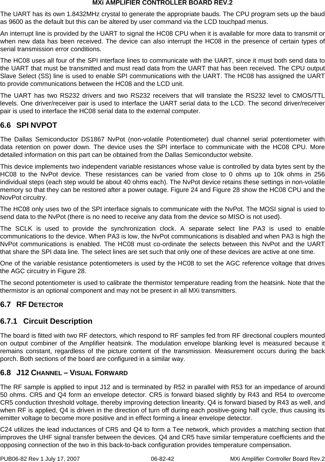
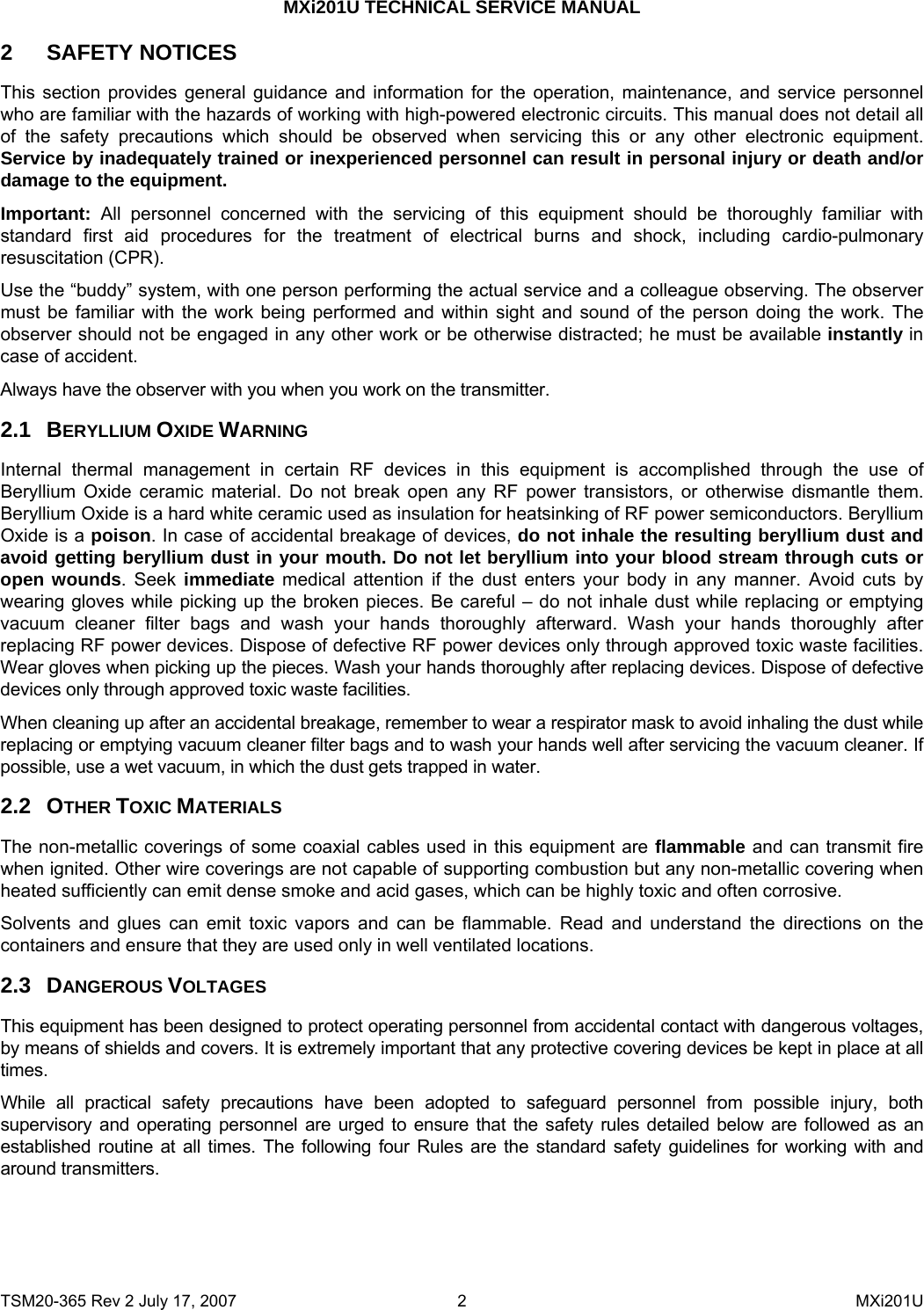
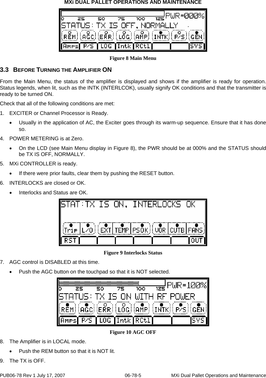
![MXi AMPLIFIER CONTROLLER BOARD REV.2 PUB06-82 Rev 1 July 17, 2007 06-82-25 MXi Amplifier Controller Board Rev.2 Figure 15 Logs Submenu Screen The logs are displayed up to three at a time, in the order in which they were detected in the controller. That is, the logs are in chronological order from the time they were received. The seventh menu button on the fourth line of the LCD shows the total number of log entries [our example shows 2 entries #=02]. A maximum of 99 log entries can be held in the log table. If the log table already contains 99 entries and a new log has occurred, the oldest log is discarded and the new log is entered into the table. In this manner the log table will hold the 99 most recent logs. In the fourth menu button line of the LCD, the first four button selections (from the left side) allow the operator to navigate through the log table when there are more than three logs. If there are three logs or less, all the entries are already displayed on the LCD. The first menu button is labeled 1ST and causes the display to return to the beginning of the log table and display the first three entries. The second menu button is labeled LAST and causes the display to jump to the end of the log table and display the last three entries. The third menu button is labeled NEXT and causes the display to scroll down one log entry. If the LCD was displaying LOGS 2-4, then pressing NEXT displays LOGS 3-5. The fourth menu button is labeled 1ST and causes the display to scroll down up one log entry. If the LCD was displaying LOGS 2-4, then pressing PREV displays LOGS 1-3. The fifth menu button is labeled CLR and causes the log table to be cleared and the LCD will have no logs to display and the count will revert back to zero #=00. As noted previously, the log count is located in the seventh menu button position. Pressing this button does not perform any function. The eighth menu button is labeled OUT and causes the LCD screen to return to the Main Menu. 3.6 GENERAL SCREEN The General submenu is entered by pressing the GEN submenu button on the main LCD screen. This submenu displays all the configuration and setup information of the particular model of MXi transmitter. The first line displays the transmitter type, the second line displays the software code and revision, the third line displays the LARCAN ID number that is used in the factory to determine options, date the boards were made and other information. This information is not really important for day to day operations but can be useful when dealing with LARCAN service in verifying the transmitter configuration. There is only one menu button option on the fourth line of the LCD screen, which is the OUT button in the eighth position. Pressing this button causes the LCD screen to return to the Main Menu. The LCD displays a typical GEN submenu as follows:](https://usermanual.wiki/Larcan/MXI201UD/User-Guide-1189565-Page-71.png)
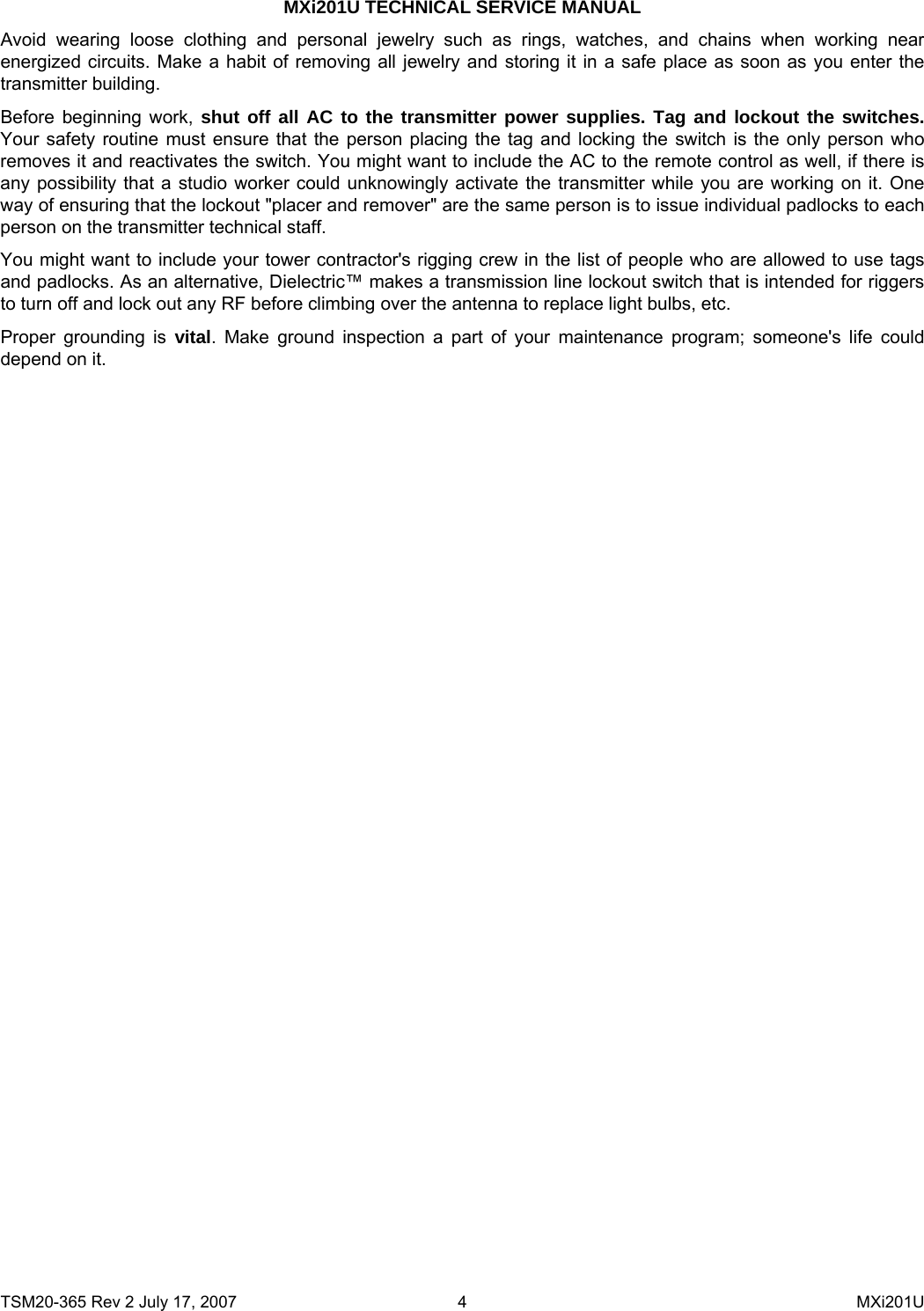
![MXi AMPLIFIER CONTROLLER BOARD REV.2 PUB06-82 Rev 1 July 17, 2007 06-82-37 MXi Amplifier Controller Board Rev.2 6 CIRCUIT DESCRIPTIONS 6.1 MC68HC908 MICROPROCESSOR The Motorola MC68HC908GT microprocessor (often referred to as the CPU or HC08) performs all of the control interface and communications in the MXi transmitter system. It is a 44-pin surface mount PLCC type device that is permanently soldered to the circuit board and is not field serviceable or easily replaced without special surface mount tooling. A brief description of the part is given in this section and a portion of the manufacturer’s documentation is given in Appendix A. More detailed information on this part can be obtained from the Motorola web site. The HC08 chip used in the MXi can come with either 8K or 16K bytes of non-volatile flash memory, which can be erased and reprogrammed to allow updating of software code or system parameters. The MXi code is typically smaller than 8k and so would fit in either size of Flash memory. The HC08 chip has a dedicated serial input pin designated as the BDM (Background Debug Mode) port that is used to program the internal Flash memory and for debug testing. The MXi is programmed at the factory and it is not expected that reprogramming would need be done in the field, although it is possible to do with the proper software. System parameters and status that need to be retained during power failures (such as the LOG entries) are also stored in the Flash memory. Most of the external pins on the HC08 are configured as programmable Input/Output (I/O) ports, where the software program determines whether a certain pin is to be configured as either an input or output. The pins on the HC08 are grouped together in sets called PORTs. These Ports will have eight pins (or fewer) to support the byte wide data path in the CPU. Port A is used for general system inputs and outputs. Port B is used as an eight-channel A/D converter to measure system telemetry values. Port C is used for general system inputs and outputs. Port D assigns four pins for the synchronous serial port (SPI) with the other four pins used for system inputs. Port E assigns two pins as a serial communications port (SCI), one pin is the external CPU clock and the other two pins used for general system inputs and outputs. The definition of each Port pin is as follows: PORT A PA0 Input or Output Jumper E3 configures as I/P or O/P PA1 Input Remote Control ON Command PA2 Input Remote Control OFF Command PA3 Output Select enable for Serial NvPot U16 PA4 Input Front Panel ON Command PA5 Input Front Panel VSWR RESET Command PA6 Input 32V Power Supply OK Status PA7 Input Remote Control VOR Status PORT B PB0 Telemetry Temperature of Heatsink [Optional] PB1 Telemetry Power Supply Current PB2 Telemetry Power Supply Volts PB3 Telemetry Cutback Volts [Scaled at half the actual value] PB4 Telemetry AGC Volts [Scaled at half the actual value] PB5 Telemetry RF Aural Power [from RF detector - Optional] PB6 Telemetry RF Reflected Power [from RF detector] PB7 Telemetry RF Forward Power [from RF detector]](https://usermanual.wiki/Larcan/MXI201UD/User-Guide-1189565-Page-83.png)
![MXi AMPLIFIER CONTROLLER BOARD REV.2 PUB06-82 Rev 1 July 17, 2007 06-82-38 MXi Amplifier Controller Board Rev.2 PORT C PC0 Output Remote Status – Error PC1 Input DipSw #1 PC2 Input Power Supply (Relay K1) ON Status PC3 Input DipSw #2 PC4 Input External #1 Interlock PC5 Output VSWR Reset Control PC6 Output PS ON Ctl +12V out [could be 24V too] PORT D PD0 SPI SS Used by UART PD1 SPI MISO Used by UART and NvPot PD2 SPI MOSI Used by UART and NvPot PD3 SPI SCLK Used by UART and NvPot PD4 Input Fan#1 Status, Active Low PD5 Input Fan#2 Status, Active Low PD6 Input Fan#3 Status, Active Low PD7 Input Fan#4 Status, Active Low PORT E PE0 SCI Transmit Data Used by LCD PE1 SCI Receive Data Used by LCD PE2 O/P Remote Status – Remote Mode PE3 Input VSWR Trip Status PE4 System Main CPU Clock – 4.9152MHz The HC08 provides two separate serial interfaces to external components, these are the synchronous peripheral interface (SPI) and the serial communications interface (SCI). The SCI implements the standard three-wire serial port (Rx Data, Tx Data and Ground) that would interface to a typical computer port. The baud is settable from 300 up to 38,400 bits per second via the LCD menus. The baud is derived from the system oscillator clock at 4.9152MHz. This frequency is recommended by the manufacturer to easily obtain the most common bauds. The SPI implements a four-wire clocked serial port that has four signals, Slave Select (SS), Master Out Slave In (MOSI), Master In Slave Out (MISO) and Serial Clock (SCLK). The HC08 is always set as the Master who initiates all serial communications. The SPI port is used to communicate with the MAX3110 UART (U2) and the DS1867 NovPot (U16). The HC08 will send out it data stream from the MOSI line and reads any responses from the external (Slave) devices via the MISO line. The SCLK is a serial clock (set for around 64K baud) that synchronizes the data transfer. The presence of this clock allows must higher data rates than the asynchronous SCI serial protocol. The SS line is a select that enables the MAX 3110 UART when low. A second individual select line from Port A (pin PA3) is used to select the DS1867 NovPot. 6.2 POWER SUPPLY VOLTAGE AND CURRENT MONITORING For the following description, refer to Figure 25 (Sheet #2 of the Schematic) in the upper section of the drawing for the power supply monitoring circuitry.](https://usermanual.wiki/Larcan/MXI201UD/User-Guide-1189565-Page-84.png)