Larcan T1000U 1000 Watt UHF Translator User Manual 01 INTRODUCTION rv1
Larcan Inc 1000 Watt UHF Translator 01 INTRODUCTION rv1
Larcan >
manual

Unit 1 – Introduction
- 11 -
2. General Technical Descriptive:
2.1. IF Modulator (for transmitter):
This is the input module. It is a professional audio and video modulator. The audio and video
signals are applied to their respective input for the modulation process in IF (41 to 47 MHz]. The audio
and video input impedances are 600 balanced Ohms and 75 unbalanced Ohms, respectively.
2.1.1. Video processing:
The video signal passes through linearity correction circuits and then is applied to the 45.75
MHz video modulator. There are Synchronizing Separation circuits that generate the auxiliary outputs
to “Automatic Circuits”. The video signal is also applied to a group delay predistortion circuit.
2.1.2. Audio processing:
The Mono-audio signal or stereo base band is applied to the module and modulates a 41.25
MHz audio carrier.
2.1.3 Module output:
Both carriers, audio and video modulated (41.25 and 45.75 MHz), are applied to the “Vestigial
Side Band Filter” (SAW Filter). At the output there is a circuit to control the IF output level.
2.2. UHF UP Converter:
2.2.1. Introduction:
This module converts an IF frequency signal into an UHF band channel, keeping its
characteristics and the same bandwidth.
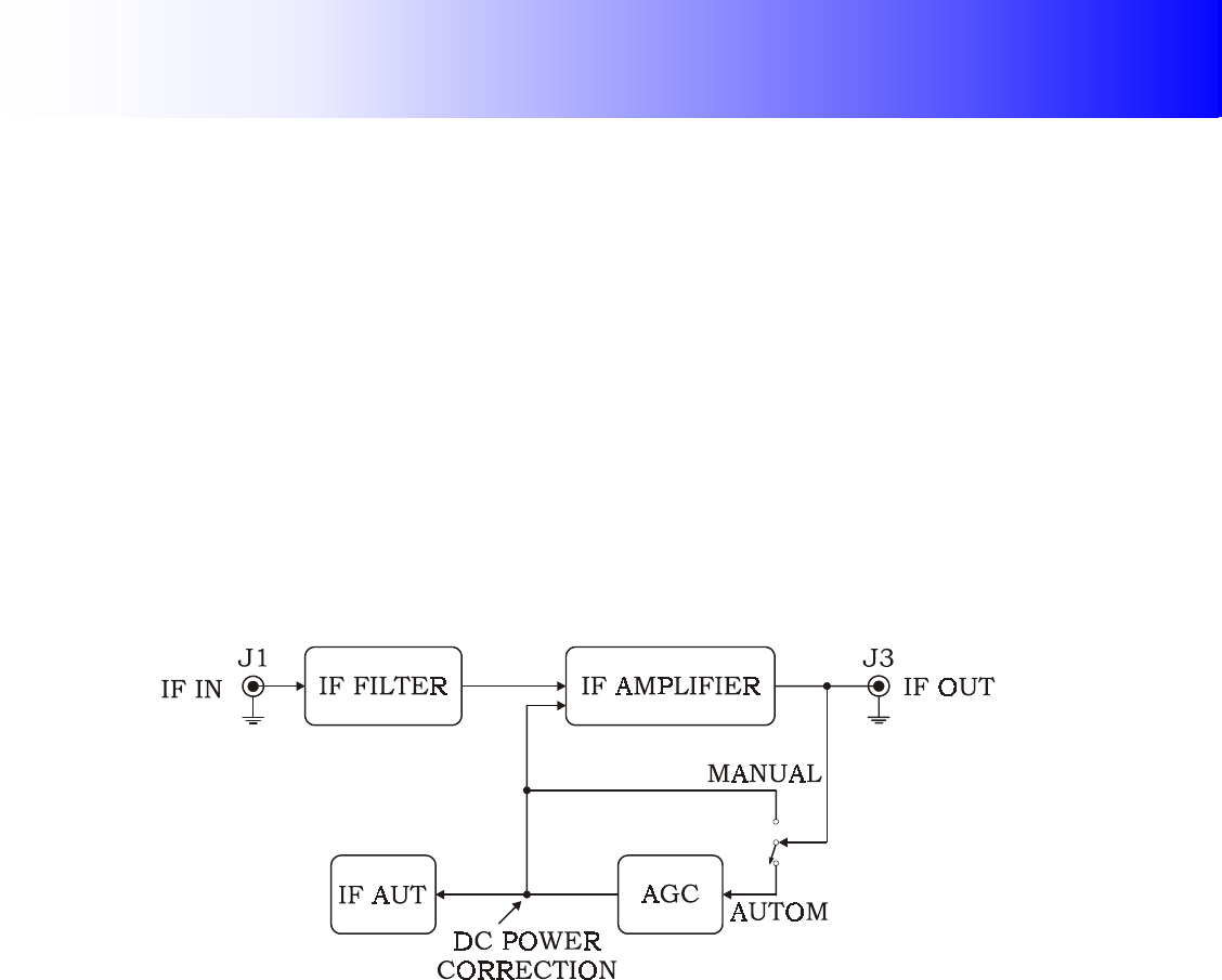
2.2.2. IF filter and AGC amplifier (for transposer):
The IF amplifier and filter module establish the adequate bandwidth for the input signal and
supply the gain in this signal, keeping the level constant through an AGC loop.
2.2.3. Technical Descriptive:
The 2nd UHF converter has an oscillator controlled by PLL (Phase Locked Loop Integrated
Circuit), which frequency is selected through the DIP switch from the Oscillator control board. When
the modulated signal in IF is received in the 2nd converter, it is filtered and applied to a mixer. The
result of this mixing is filtered (channel filter) and supplied to the following modules of the equipment,
in the selected channel.

Unit 1 – Introduction
- 12 -
2.3. Amplifier Levels:
2.3.1. Comment/Composition/Origin:
The RTU1000T is composed of four 250W amplifier modules that are combined through 3dB
hybrid circuits. A 50W amplifier and 1: 4 hybrid module excite the final modules.
All the amplifiers are completely in solid state.
2.3.2. Protections/Signaling:
Each 250W amplifier has a VSWR protection (Voltage Stationary Wave Ratio), temperature and
limiting power. The output power, VSWR, temperature, current and module voltage can be monitored
through a DB9 connector in the front panel. In the frontal panel also there is the normal power
indication (Green Led), low power (red led) and excessive VSWR (red led). In the output there is the
video and audio power monitoring, antenna VSWR, power supply current and voltage, VSWR
indications, power supply temperature, signal absence, over voltage and over current.
2.4. Notch filter:
It is used to assure the operation of other transmitters in adjacent channels. It is composed by 7
mechanical cavities, 6 are syntonized in the spurious frequencies and 1 in the 2nd harmonic.
Unit 2 – IF Modulator
- 2 -
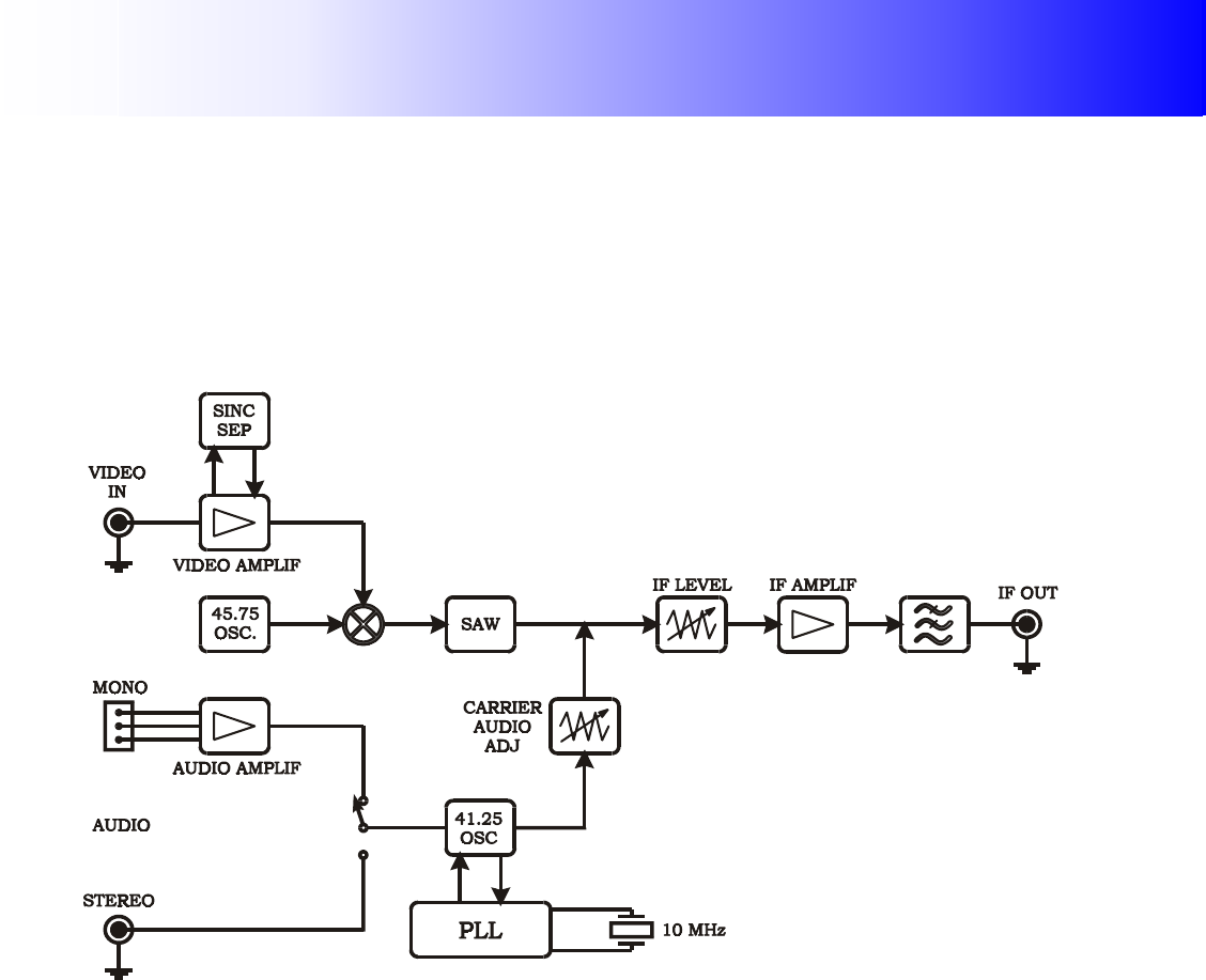
1. Audio and Video Modulator:
1.1. Function:
This module function is to generate two carriers: one in 45.75 MHz and the other in 41.25 MHz.
The first is modulated in AM-VSB by a video signal and the other one is modulated in frequency by an
audio signal.
1.2. Block Diagram:
1.3. Technical Description:
1.3.1. Video Modulator:
The transistor Q1 oscillates in the crystal frequency (45.75 MHz - IF video), and the transistor
Q2, with high input impedance, guarantees the isolation to the oscillator Q1 output. The frequency
accuracy is adjusted in the variable inductor L1. The input video signal, with adjustable level in R27
(front panel), is applied to the high impedance input push-pull amplifier formed by transistors Q6 and
Q9. The amplifier output signal modulates in amplitude, in the mixer M1, the video carrier.
The integrated circuits IC18 to IC21 form a group delay predistortion circuit. The syntonized
cells, at the video bandwidth, cause an advancement of 170 ns at 3.58MHz. This video pre-distortion is
inserted in the circuit through jump’s JP5 and JP6. The adjustable attenuator R146 allows equalizing
the video level when the pre-corrector circuit is turned off.
The transistor Q12 receives the video signal, invertes its phase and applies it to the IC7
amplifier. This amplifier causes a non-linear enlargement to the video signal emphasizing the
synchronizing pulses. This signal is clamped in 0.7V by the D5 and is compared to 0.3V (due to diode
D4) in the comparator circuit IC6. In this manner, at the IC6 output, there will be only synchronizing
pulses. These pulses are applied to the IC5 (mono-stable) in the negative transition to generate
clamping pulses. The clamping pulses commute the transistor Q10 that switches the video signal
clamping it to the blanking level through R45. This adjustment allows choosing the point of modulation
in the mixer for a better linearity. If there is lack of clamping pulses, the Q11 transistor commutes,
allowing adjusting through R44 the level of the video carrier without modulation.
The integrated circuit IC9B receives the clamping signal detected through D7, changes its state
and commutes the transistor Q13. It allows switching the external circuits connected to the Automatic
output. The led in the panel shows this operation, when it is green it indicates video on. This circuit
presents about 60 seconds delay time approximately.

Unit 2 – IF Modulator
- 3 -
The video signal peak is detected through IC8 and through IC9 and it is differentiated with the
level adjusted through R45, in order to extract the dc component.
The IC9A output has a dc level related to the video signal not taking into account the
synchronizing pulses. The 100% video measurement is adjusted through R72 in the meter with a video
signal with 100% APL. The C118 e L18 components form an ICPM corrector circuit that allows
correcting a non-desirable phase-shift at the video carrier caused by the modulating signal.
The modulated video carrier is amplified by IC1 and the SAW filter FL1 filters this signal giving
the final characteristics of the desired modulation, i.e., AM_VSB (amplitude modulation with vestigial
side band). The amplifiers IC2, IC3 and IC4 produce the necessary gain to signal, in order to
compensate the losses in SAW filter and deliver a 0 dBm output level. The output signal level is
adjustable by R12 (front panel), which controls the PIN diode conduction (D1). The trimpot R13 limits
the maximum IF output level and the circuit formed by transistor Q19 and capacitor C120 increases
slowly the output level to eliminate high frequency peaks when the equipment is turned on.
The IF signal, after amplification, passes through a low-pass filter, formed by L6, L7, C21, C22
and C23 to eliminate harmonic signals. Part of this signal is sent to the detector circuit formed by
transistors Q3 and Q4 to measure the IF signal in the panel. The trimpot R24 allows adjusting the
reading level through the meter.
1.3.2. Audio Modulator:
The transistor Q14 and associated components generate the audio carrier. The applied voltage
to the varicap diode D10 controls its frequency. The amplifiers IC12 and IC13 increase the signal level
and through the trimpot R108 is applied to the IF amplifier to be delivered at the output. A sample of
this signal is delivered to the “prescaler” IC14 through R108. It divides the signal into 64 and delivers it
to PLL (integrated IC15). The PLL divides again this signal, now into 66, and compares it with a
reference signal in phase, resulting a voltage proportional to the difference of the phase between the
signals; this voltage is filtered and applied to diode D10 to correct the frequency. The reference
frequency for PLL is generated at the integrated circuit itself that oscillates at 10 MHz and divides it
into 1024. The oscillator crystal is found in a thermal chamber, which is controlled by Q15 and by
thermistor NT1, for better frequency stability. The trimmer C90 allows the fine adjustment of this
carrier frequency (41.25 MHz). If the circuit cannot correct the frequency, the transistors Q17 and Q18
are commuted to turn on the frequency error red led.
The audio signal that will cause the modulation in frequency in this carrier may come from the
mono audio input or stereo audio input. It is possible to select it through jump JP3.
The mono audio input circuit has an unbalanced amplifier IC10 and pre-emphasis circuit. It is
possible to turn off the pre-emphasis through jump JP2. The trimpot R92 (front panel) adjusts the
audio level that will cause the correct modulation index. The integrated circuit IC17 and associated
components form a peak detector of audio signal and a trimpot R117 allows adjusting 100% at the
meter for the correct deviation. The battery input (+36V) through D16 and fuse F1 connects through
connector CN2 the power supply FTE017 (optional).
Obs: The circuit diagram is divided into four parts.
Unit 2 – IF Modulator
- 18 -
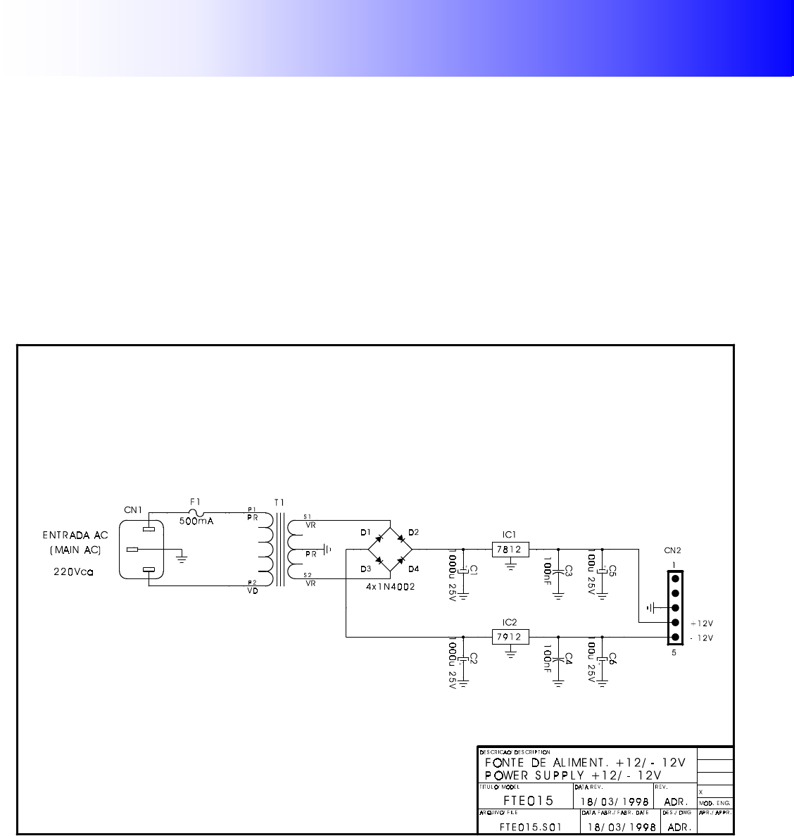
8. Power Supply:
8.1. Function:
The power supply function is to generate +12V and -12V voltage suitable to supply the
modulator.
8.2. Technical Description:
The transformer T1 reduces the input voltage for the rectifiers D1 to D4. The positive and
negative voltage obtained after the rectification and filtering through C1 and C2 are regulated through
IC1 and IC2 to obtain +12V and -12V voltage to supply the Modulator.
8.3. Circuit Diagram FTE015:
Unit 2 – IF Modulator
- 20 -
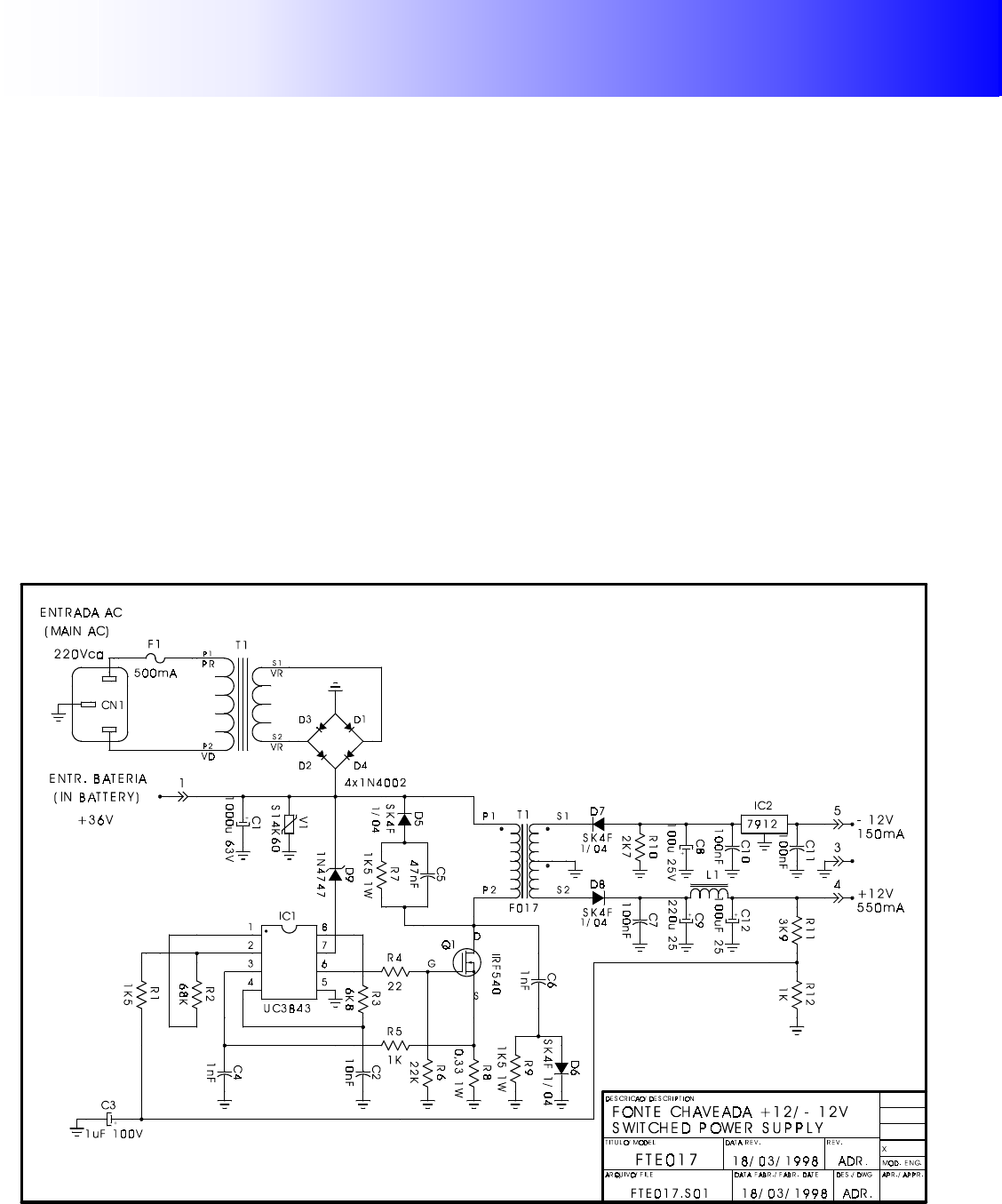
9. Power Supply (optional):
9.1. Function:
The switched power supply has the function to generate +12V and -12V voltages from the input
voltages AC or from the +36V battery (opc).
9.2. Technical Description:
The input voltage, after transformer T2 and diodes D1 and D4, supplies the PWM IC1. If there is
no AC the battery voltage supplies the circuit.
The pulses generated by IC1 commute the transistor Q1 and switch the voltage over the primary
T1 at 25 KHz frequency.
The induced pulses that are in the secondary are rectified by D7 and D8 and filtered by C8 e C9. The
regulator IC2 assures the -12V regulated voltage. A voltage sample after L1 supplies the IC1 control
input, through the divider R11 and R12. The pulses that are generated for IC1 have their width
changed in function of the received sample, canceling, in this manner, any variation in the +12V
voltage. The resistor R9 supplies a sampled voltage related to the current which circulates in the output
to the IC1, pin 3. This input protects the over current, reducing the +12V voltage.
9.3. Circuit diagram FTE017:
Unit 2 – IF Modulator
- 23 -
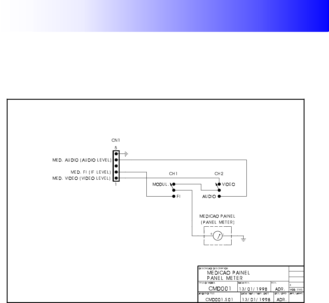
10. Meter Circuit:
10.1. Function:
The meter circuit allows, through the selector switches and meter, the measurements of the
video modulation, audio modulation and the IF level.
10.2. Circuit diagram CMD001:

Unit 3 – Channel UP Converter
- 2 -
1. Channel UP converter:
1.1. Introduction:
This module converts an IF signal, into “a” UHF band channel, maintaining its characteristics
and the same bandwidth.
1.2. IF filter and amplifier AGC (for transposer):
The filter and IF amplifier establish the necessary bandwidth to the input signal and supply a
gain in it, maintaining a constant level, through an AGC loop. It is used only in the transposer
equipments.
1.3. IF pre-distortion:
The IF module pre-distortion corrects the intermodulation, the differential gain, the differential
phase and the synchronism compression. This correction is done by pre-distortion on IF level (41-47
MHz). This module is placed after the audio and video modulator and before the channel converter
module.
1.4. Automatic Level Control (ALC):
This module maintains the output peak power at its nominal value, even if there is gain
variation due to the temperature and power supply variations.
It allows a maximum correction of ±1dB.
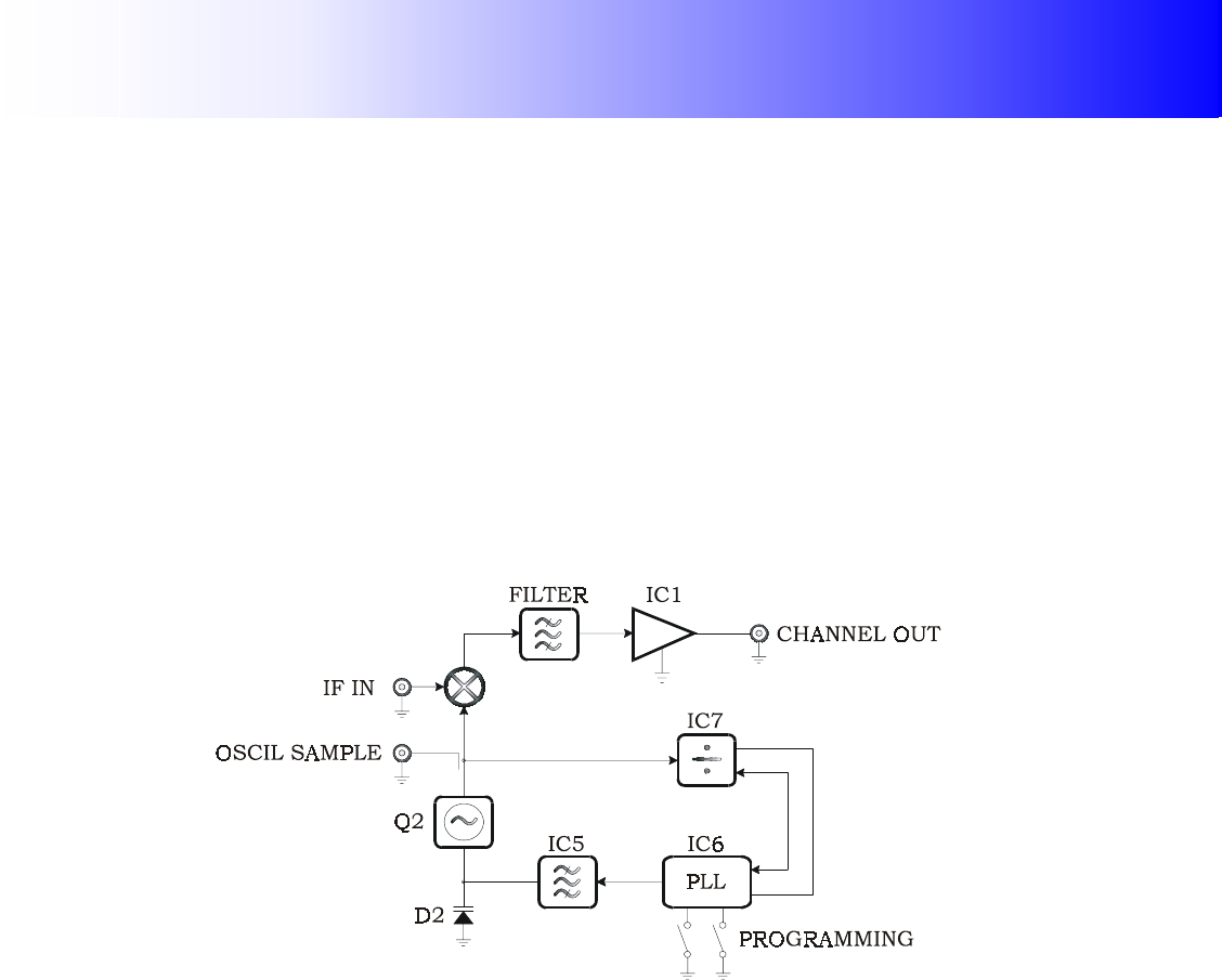
1.5. Channel converter:
The UHF channel UP converter has an oscillator that is controlled by PLL, whose frequency
operation is selected by DIP switch from the Local Oscillator control board, according to the channel
programming chart.
1.6. Protections/signals:
The channel UP converter has in its front panel a PLL (Phase Locked Loop) alarm led that shows
if the converter is out of the operation frequency.
Unit 3 – Channel UP Converter
- 6 -
3. IF filter amplifier:
3.1. Function:
The IF filter establishes the adequate bandwidth to the input signal and the IF amplifier supplies
the gain for this signal, maintaining a constant level, through AGC loop.
3.2. Technical Characteristics:
Central Frequency __________________________________________________________________________ 44 MHz
Bandwidth __________________________________________________________________________________ 6 MHz
Input and Output impedance ______________________________________________________________ 50 Ohms
Maximum output level ______________________________________________________________________ +3 dBm
Linearity _________________________________________________________________ + or – 0.25 dB in ± 3 MHz
Maximum gain _______________________________________________________________________________ 60 dB
AGC band ____________________________________________________________________________________ 50 dB
Supply ______________________________________________________________________________ +12V at 250mA
3.3. Block Diagram:
3.4. Technical description:
3.4.1. IF Filter:
The input signal is applied by J1. The integrated circuit IC1 amplifies the applied signal to the
IF filter.
The function of the circuit that is formed by C7, L3, C8, C9, L4, C10, C11, L5, C12, C13, C14
and C16 is to determine the IF amplifier operation bandwidth. This filter is adjusted to obtain a 6MHz
bandwidth.
3.4.2. IF amplifier:
The IF signal received from IF filter is, through C17, connected to the adjustable attenuating
loop, that is formed by diodes D2, R9, D4 and D3. After the attenuating loop, the signal is amplified by
the integrated circuit MAR-7 (IC2).
The amplified signal passes through another attenuating loop, formed by diodes and resistors
D5, R14, D7 and D6, and it is connected by the capacitor C28 to the integrated circuit MAR-6 (IC3),
and finally, through capacitor C29, reaches the integrated circuit MAR-7 (IC4).
A sample signal from the output signal is taken from the resistor R45; after, it is amplified by
transistor Q4 and detected by the diodes D10 and D11. The detected signal by the diode D11 is
supplied, by the emitter follower Q3, to check the IF level in the panel.
The integrated circuit IC5-B supplies in its output a dc level, that is the function of the received
signal J1. The diode D1 and L9 act respectively in the polarization of the attenuating loops, altering the
final gain of the IF amplifier. When JP2 is in the AUT position, this dc level is proportional due to the
detected signal by the diode D10, maintaining the IF level constant in the output J3.
The IC5-A output level is the result of input levels voltage comparison between pins 3 and 2.
This way we can determine the operation point of the IF command adjusting R21. Through CN3-1 the

Unit 3 – Channel UP Converter
- 7 -
following circuits are enabled.

Unit 3 – Channel UP Converter
- 12 -
4. IF Pre-distortion linearity:
4.1. Function:
It corrects the non-linearity and/or intermodulation that are generated at the final stage of the
transmitter amplification.
4.2. Technical characteristics:
Frequency band: ______________________________________________________________________ 41 to 47 MHz
Input level: ____________________________________________________________________ -4.0 dBm ± 1.0 dBm
Output level (adj): __________________________________________________________________ + 3.0 dBm (max)
Input/Output Impedance:___________________________________________________________________ 50 ohm
Supply: _______________________________________________________________________________________ +25V
4.3. Technical Description:
IF signal applied to the input J1 is amplified by Q1, and in Q2 is divided in order to supply two
circuits, a linear one and a non-linear one.
The linear circuit has about a 40 ns delay line to compensate the delay caused in the non-linear
circuit. After the delay line, the signal is inserted through trimpot R13 in the adder circuit that is
formed by Q4 and Q5.
The non-linear circuit causes a distortion in the signal trough D3 and D4 that have its
conduction region determined by trimpots R11 and R29. This signal, distorted and amplified by Q7 and
Q8, is put in phase by equalizer circuit formed for L11, C29, R40 and R41, again amplified for Q9, via
trimpot R50 and transistor Q10 and finally is added to the linear signal.
The composed IF signal passes by the attenuator circuit, and its level is adjusted by R44, and
amplified by IC1 when it is delivered to output J2.
4.4. Adjustment Procedure:
The signal should be constantly checked by the spectrum analyzer using the red pattern
modulated signal.
1) Insert the circuit in the system when the IF level is about –3.0 dBm in the input and all the
trimpots are in the minimum.
2) Adjust trimpot R44 to 80% of its course approximately, then increase the level in R13 until
the nominal power is reached.
3) Adjust trimpots R11 and R29 in order to cause the needed distortion to cancel the distortion
that comes from the amplifying final stage, adjusting the level of this signal in the trimpot R50 and
compensating the power variation in the trimpot R13, in order to maintain it as a nominal one. Adjust
the inductor L11 to obtain the distorted signal phase inversion that will be inserted in the system.

Unit 3 – Channel UP Converter
- 17 -
5. Automatic Level Control (ALC):
5.1. Function:
The Automatic Level Control corrects the transmitter output peak sync power due to the
variation gain of the amplifiers.
5.2. Technical Description:
This circuit has a total attenuation of 1dB, allowing controlling the power to positive and
negative variation of 0.5dB.
The command occurs through the obtained voltage from the TV monitor through wire identified
by the CAP cord. If the Turn on/turn off switch in the panel is OFF, it allows adjusting the output
power, as it fixes the CP input in 3.7V. We can observe in the circuit the variable attenuator by the
diodes PIN formed by diodes D1, D2 and D3, and capacitors C10, C11 to C14 and resistors R14 and
R15.
The Pin diodes current occurs through the integrated circuit IC1A, by shock CH1. The TV
monitor CAP command voltage supplies the IC1A inverter gate through R1. The integrate circuit IC1A
amplifies this voltage increasing its range from –0.5 to -10V.
The integrated circuit IC1B receives this voltage of –0.5 to -10V by R10, adding it to a pre-fixed
value R7, R8 and R9. This causes the IC1B output variation from –1.5 to -8V approximately, causing
the circuit attenuation to PIN diode, which does not exceed a total variation of 1dB.
The divisor formed by R18, R19 and R20, allows obtaining the reference voltage (REF) to
calibrate the transmitter power in the ALC OFF situation.
5.3. Adjustment Procedure:
a) Turn the switch to OFF position (in the panel).
b) Adjust R19 to a 3.7V reading in a digital multimeter in the output REF pin.
c) Adjust the sweep generator, the detector and the oscilloscope to 0dBm IF frequency, inserting the
circuit.
d) Through CN1 turn on R1 to ground.
e) Verify if the attenuation is inferior to 1dB in the oscilloscope and memorize the response.
f) Through CN1, turn on R1 to -12V.
g) Through R9 adjust the attenuation to 1dB in the oscilloscope.
h) Turn off CN1 and adjust R5 to half of the range in the oscilloscope.
i) Insert the circuit between the modulator and the channel converter.
j) The IF level is adjusted to nominal power when the switch is in OFF position.
k) Change to the ON position, verifying the output power.
Unit 3 – Channel UP Converter
- 21 -
6. Channel UP Converter:
6.1. Function:
The channel UP converter function is to convert the IF frequency (41 to 47 MHz) to a determined
channel in UHF.
6.2. Technical Characteristics:
Input frequency band: ________________________________________________________________ 41 to 47 MHz
Output frequency band:_____________________________________________________________ 470 to 890 MHz
Gain: _________________________________________________________________________________________ 0 dB
Input/Output Impedance: _________________________________________________________________ 50 Ohms
Channel bandwidth: _________________________________________________________________________ 6 MHz
Consume: __________________________________________________________________________ +12V at 150mA
6.3. Block Diagram:
6.4. Technical Description:
The oscillator, transistor Q2, generates a low noise signal in the used frequency band. Its
frequency is determined by the control voltage applied to diode varicap D2. The amplifier IC3 receives
the oscillator signal and provides load isolation and, the amplifier IC2 delivers to the mixer a +17 dBm
level. A sample from the oscillator signal is, through R25, delivered to IC7 prescaler, that divides the
signal into 64 and 65, according to the control that comes from PLL, integrated circuit IC8. PLL receives
the prescaler signal and divides it according to the external programming (1 to 8), and compares it in
phase to a reference signal controlled by crystal generated by the own integrated circuit.
In the integrated circuit output results a proportional voltage that is the phase difference among
the signals. This voltage is filtered by IC5 and applied to diode D2 for the frequency correction
The mixer MX1 receives IF signals and the local oscillator, and generates through the signal
beating the desired channel. The conversion loss in the mixer is aproximately 8dB at most. The signal
after the mixer passes through the channel filter that rejects the local oscillator and the undesirable
product in the conversion. The amplifier IC1 compensates the mixer and the channel filter losses.
6.5. System alignment:
1. Program the oscillator according to the given channel chart and with a multimeter in PT2,
adjust trimmer C21 to a 4.5V reading. The led helps the adjustment, when it is turned off it indicates
that the oscillator is in the desired frequency. In the point meas. at oscillator shows 0.5V level
indicating the RF presence that comes from the local oscillator.
2. Put the sweep generator in the IF band in 41 to 47 MHz, and apply to the IF input, in JP1.
Adjust the channel filter to the maximum gain and a better linearity, with the detector in the channel
output.
Unit 3 – Channel UP Converter
- 28 -
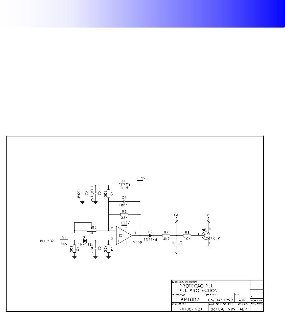
7. PLL protection:
7.1. Function:
This circuit function is to turn off the transmitter.
7.2. Technical Description:
The DC voltage that comes from the channel converter, more precisely from the channel
converter Led diode, is applied to the comparator through diode D1 by resistor R1 and reaches circuit
integrated IC1pin 3.
Through the adjustment in the trimpot R3, we can act in the integrated circuit comparison,
moving pin 1 to high level (operational gain X comparing voltage). Then, through diode D2 this voltage
is applied to CA output (High level) or CB (Low level), by the transistor Q1 collector saturation.
7.3. Circuit diagram PRT007:

Unit 3 – Channel UP Converter
- 30 -
8. UP Converter supply -12, +12 and +24V:
8.1. Function:
The power supply function is to generate -12V, +12V and +24V voltage suitable to supply the UP
Converter.
8.2. Technical Description:
The main AC input voltage is reduced by the transformer T1.
T1 has two secondarie winds, one for the +24V and the second for the +12V and –12V supplies.
D1, D2, D3 and D4 rectifiers the secondary voltage that is filtered by the capacitor C1. IC1 is a
linear regulator that feeds +24V at the output.
D5 and D6 are the retifier diodes for the positive voltage filtered by C4.
IC2 is a linear regulator for the +12V output supply.
In the same manner there are a rectifier and a linear regulator for the negative voltage –12V.

Unit 4 – 50W Exciter
- 2 -
1. 50W Exciter:
1.1. Introduction:
This module amplifies the signal power that comes from the channel converter, to the 50 W
level, maintaining its characteristics and the same bandwidth.
1.2. Protections and Monitoring:
We have for these functions:
VSWR Circuit: it protects the amplifier module transistors, when the output stationary wave is
superior to 4%. This circuit acts in the output transistors gates.
Temperature Circuit: it acts in the output transistors gates when the heat sink temperature is above
56°C
Forward RF Power Circuit: it acts in the output transistors gates when the output RF power
overcomes the pre-fixed value limiting, in this manner, the maximum RF forward power.
1.3. Power Supply input:
This circuit supplies information from the amplifier currents.
1.5. Amplifier Stages:
This module has two UHF amplifier stages in cascade, the first of 2W and the second of 50W.

Unit 4 – 50W Exciter
- 5 -
3. Amplifier protection:
3.1. Function:
This module function is to protect the amplifier modules against an excessive VSWR, RF power
and temperature.
3.2. Technical Description:
The informations from forward RF power and VSWR are obtained through the Directional
Coupling detectors from the amplifier output.
The proportional voltage to the RF forward power supplies the isolator amplifier integrated
circuit IC5A. This amplifier output, supplies IC5B and IC2A comparator circuits. The integrated circuit
IC5B acts as a RF power limitator, and if the RF forward power overcomes the pre-fixed value by
trimpot R31, transistor Q1 conducts by diode D3, and resistor R39, removing the gate polarization
voltage from the 50W final amplifier. The integrated circuit IC2A compares the RF forward power to an
adjusted value in –3dB by trimpot R10, so that the RF forward power green Led lights in the panel. The
integrated circuit IC2B is an inverter amplifier, be that, when the RF forward power drops lower than –
3dB, its output reaches +12V what lights the RF forward power red Led in the panel.
The VSWR proportional voltage supplies the insulator amplifier integrated circuit IC4A. The
IC4A output supplies the IC4B comparator input and also the monitoring in the panel by R1.
If the RF signal exceeds the value that is pre-fixed by trimpot R24, the VSWR Led in the panel
lights and transistor Q1 conducts by diode D5 and resistor R39, removing the polarization from the
output amplifier transistor.
A temperature sensor protects the temperature. This sensor supplies a proportional voltage to
the temperature monitored from 10mV/°C, be that, if the temperature is 50°C we have 500mV.
Through the IC3A isolator amplifier, this voltage is compared to a pre-determined value by trimpot R17
and it is also sent to the frontal panel. The integrated circuit IC3B lights the temperature Led in the
panel and by transistor Q1, diode D4 and resistor R39, it is removed the polarization from the final
amplifier transistors.
The diodes D1 and D2 and the fixed voltage regulator IC1 are responsible for the +12V power
supply that supplies the several protection IC’s.
Unit 4 – 50W Exciter
- 9 -
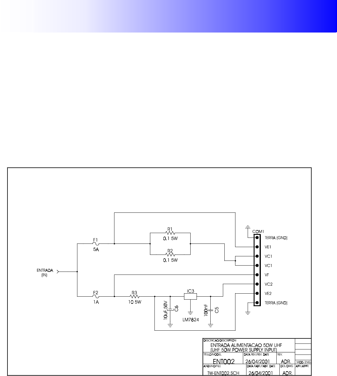
4. Power supply input:
4.1. Function:
This circuit function is to protect the power supply, if there is a short-circuit and provides the
amplifier current monitoring.
4.2. Technical description:
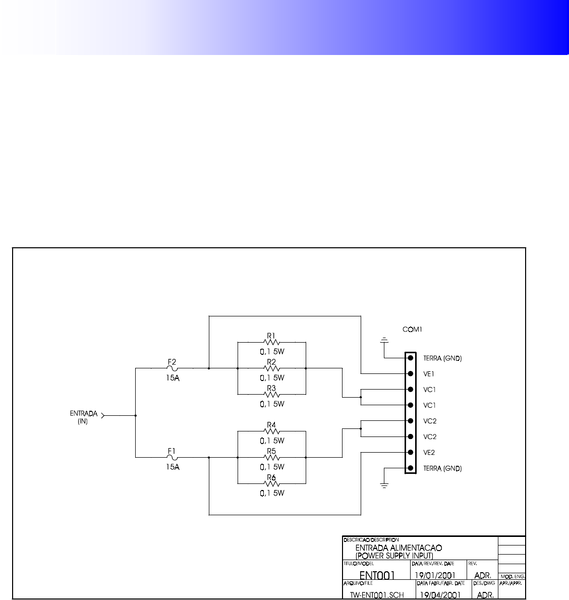
The +32Vdc voltage that comes from the three-phase fixed power supply supplies the fuses F1
and F2.
The fuse output F1, by resistors R1 and R2, supplies the 50W final amplifier. The amplifier
current can be monitored by the voltage drop over R1 and R2.
The fuse output F2, by resistor R3, supplies +24Vdc power supply regulator integrated circuit
IC3. Also, through the voltage drop over resistor R3, the 2W amplifier current can be monitored.
4.3. Circuit Diagram ENT002:

Unit 4 – 50W Exciter
- 11 -
5. 2W Amplifier:
5.1. Function:
The 2W UHF amplifier stage amplifies the channel converted to 2W maximum level.
5.2. Technical characteristics:
Gain: ________________________________________________________________________________________ 30 dB
Supply: _____________________________________________________________________________________ +32Vdc
Total current: ___________________________________________________________________________________ 1 A
5.3. Technical Description:
This module is composed of driver amplifier IC1 and the final amplifier Q1.
Trimpot R4 sets the quiescent current of Q1 and D1 and allows controlling the output power for
protection purposes.
At the input, there is a local oscillator filter TLE, C4 and C5.

Unit 4 – 50W Exciter
- 14 -
6. 50W amplifier:
6.1. Function:
The 50W exciter amplifier stage, receives the 2W amplifier signal and delivers it to 1:4 divider of
250W amplifiers with a maximum 50W power.
6.2. Technical characteristics:
Input power: ____________________________________________________________ 2W (Sync and Audio carrier)
Output power: ______________________________________________________________________ 50W Peak Sync
Gain: ________________________________________________________________________________________ 18 dB
Supply: _____________________________________________________________________________________ +32Vdc
Total current: ___________________________________________________________________________________ 5 A
Setting temperature:___________________________________________________________________________ 56°C
6.3. Technical Description:
This module is composed by a LDMOS transistor.
Trimpot R4 sets the quiescent current of Q1 and D1 allows controlling the output power for
protection purposes.

Unit 5 – 250W Amplifier
- 2 -
1. 250W Amplifier:
1.1. Introduction:
This module amplifies the RF power that comes from 1:4 divisor to 250W, then they are
combined to obtain the 1000W RF power, maintaining its characteristics and the same bandwidth.
1.2. Protections and Monitoring:
For these functions, we have:
VSWR Circuit: it protects the amplifier module transistors, when the output stationary wave is
superior to 4%. This circuit acts in the output transistors gates.
Temperature Circuit: it acts in the output transistors gate when the heat sink temperature is above
56°C.
Forward power circuit: it acts in the output transistors gates when the RF output power exceeds the
pre-fixed value, this way limiting the maximum RF power.
1.3. Power supply input:
The protection fuses are in this circuit.
This circuit supplies the informations about the amplifier currents.
1.5. Amplifier stages:
Two 125W amplifier modules are used in parallel. This module uses 4 transistors MRF 373 A. Its
gain is approximately 18 dB in AB class.

Unit 5 – 250W Amplifier
- 5 -
3. Amplifier protection:
3.1. Function:
This module has the function to protect the amplifier modules against an excessive VSWR, RF
power and temperature.
3.2. Technical Description:
The informations from forward RF power and VSWR are obtained through the Directional
Coupling detectors from the amplifier output.
The proportional voltage to the RF forward power supplies the isolator amplifier integrated
circuit IC5A. This amplifier output, supplies IC5B and IC2A comparator circuits. The integrated circuit
IC5B acts as a RF power limitator, and if the RF forward power overcomes the pre-fixed value by
trimpot R31, transistor Q1 conducts by diode D3, and resistor R39, removing the gate polarization
voltage from the 50W final amplifier. The integrated circuit IC2A compares the RF forward power to an
adjusted value in –3dB by trimpot R10, so that the RF forward power green Led lights in the panel. The
integrated circuit IC2B is an inverter amplifier, be that, when the RF forward power drops lower than –
3dB, its output reaches +12V what lights the RF forward power red Led in the panel.
The VSWR proportional voltage supplies the insulator amplifier integrated circuit IC4A. The
IC4A output supplies the IC4B comparator input and also the monitoring in the panel by R1.
If the RF signal exceeds the value that is pre-fixed by trimpot R24, the VSWR Led in the panel
lights and transistor Q1 conducts by diode D5 and resistor R39, removing the polarization from the
output amplifier transistor.
A temperature sensor protects the temperature. This sensor supplies a proportional voltage to
the temperature monitored from 10mV/°C, be that, if the temperature is 50°C we have 500mV.
Through the IC3A isolator amplifier, this voltage is compared to a pre-determined value by trimpot R17
and it is also sent to the frontal panel. The integrated circuit IC3B lights the temperature Led in the
panel and by transistor Q1, diode D4 and resistor R39, it is removed the polarization from the final
amplifier transistors.
The diodes D1 and D2 and the fixed voltage regulator IC1 are responsible for the +12V power
supply that supplies the several protection IC’s.
Unit 5 – 250W Amplifier
- 9 -
4. Power supply input:
4.1. Function:
This circuit function is to protect the power supply, if there is a short-circuit and provides the
amplifier current monitoring.
4.2. Technical description:
The +32Vdc voltage that comes from the three-phase AC power supplies the fuses F1 and F2.
The F1 fuse output by resistors R4, R5 and R6 supplies the left 125W amplifier.
The F2 fuse output, by resistors R1, R2 e R3 supplies the right 125W amplificer.
4.3. Circuit Diagram ENT001:

Unit 5 – 250W Amplifier
- 11 -
5. 250W amplifier:
5.1. Function:
Its function is to amplify the power that comes from 1:4 divisor to the 250W output level.
5.2. Technical characteristics:
Power supply: ________________________________________________________________ 32Vdc 20 A maximum
Output power:____________________________________________________________________ 250W (Peak Sync)
Gain: ________________________________________________________________________________________ 18 dB
Setting Temperature: __________________________________________________________________________ 56°C
5.3. Technical Description:
The UHF 250W amplifier is formed by the combination of two 125W amplifiers.
At the input and output there are two 3 dB hibrid couplers with the rejection loads R1 and R14.
The signal splitted by the input 3 dB coupler feeds the two 50W amplifiers through C1 and C2.
At the input of each 50W amplifier there is a balun L1 and L2 that splittes the signal again for
two transistor Q1, Q2 and Q3, Q4 respectively.
The amplified signals through the baluns L5 and L6 are combined in the final 3 dB coupler with
the coupling capacitors C28 and C34.
The bias circuit is formed by resistores R12, R13 and zener diode D3 that generates a +15Vdc.
Through trimpot’s R6 and R7 the bias voltage for the transistor’s gate are adjusted.
The diode D1 and D2 allows a protection, for the amplifier, reducing the bias voltage and the
gain of the amplifier.

Unit 6 – +32V power supply
- 2 -
1. +32V Power Supply:
1.1. Introduction:
The function of this module is to provide a +32Vdc voltage at a 90 A maximum current. For this,
it is used a three-phase rectifier totally controlled by 6 SCR diodes.
1.2. +32V three-phase controlling power supply:
This circuit controls the SCR diodes trigger angle from the rectifying bridge, allowing to regulate
the power supply for the input and load voltage variation as well as the over current protection, over
voltage, the SCR’s temperature and phase fail.
1.3. Transient suppressor:
The transient suppressor eliminates the high frequency transients generated by the SCR diodes
fast commutation.
1.4. Temperature control:
This circuit controls the power supply rectifying module temperature, decreasing the SCR trigger
angle and consequently the power supplied to the load.
Unit 6 – +32V power supply
- 3 -
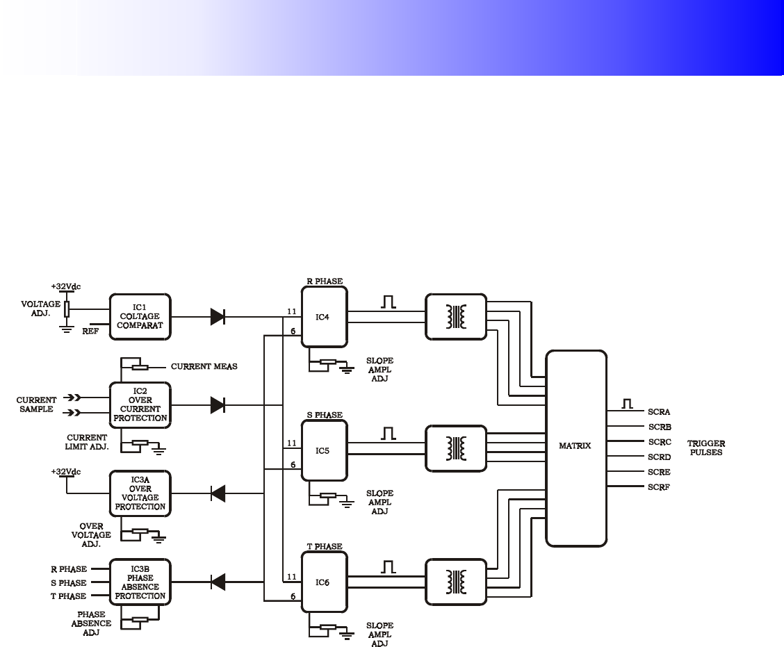
2. +32V Three-phase control power:
2.1. Function:
The module three-phase control power function is to generate synchonized triggers pulses to the
rectifier bridge power SCR. This circuit is also responsible for the over current, the over voltage and fail
phase protection.
2.2. Block Diagram:
2.3. Technical Description:
The three-phase power control is obtained by three integrated circuit IC4, IC5 and IC6.
Each integrated circuit is synchronized with its respective phase through resistors R77, R59,
R45 and limiting diodes D34, D35,D29, D36, D16 and D37.
In the phase controller integrated circuit output we have the current amplifiers Q2, Q3, Q4, Q5,
Q6 and Q7 that supply the pulse transformers with secondary double T1, T2, T3, T4, T5 and T6.
Through diodes D4, D3, D5, D6, D7, D8, D9, D10, D11, D12, D13 and D14 is produced the
trigger pulse matrix that will supply 6 SCR’s Gates from the three-phase rectifying bridge.
The trigger angle control is obtained from Pins 11 from the phase controllers integrated circuits.
The integrated circuit IC1 is responsible for the power supply stabilization, since it compares
sample voltage via resistor R2 and adjustment trimpot R68 with the 3.1V reference power obtained by
pin 8 from integrated circuit IC4. In PT4 we can monitor the control power, and the higher is the
voltage, the lower is the trigger angle from SCR’s, be that, the output voltage is lower.
The integrated circuits IC2A and IC2B provide the over current measurement protection. The
voltage drop obtained by current sensor supplies the integrated circuit input IC2A through ISC and
ISP.
In the integrated circuit IC2A (pin 1) we have a proportional voltage provided by the power.
This voltage supplies the meter through R72 and R53 and the comparing integrated circuit
input IC2B. IC2B compares the adjusted reference through trimpot R9 with the IC2A output.
If the current exceeds the determined value by R9, the IC2B integrated circuit output by diode
D30, acts in the phase control pin from the phase controller integrated circuits IC4, IC5 and IC6
decreasing the conducting angle and this way reducing the output voltage.

Unit 6 – +32V power supply
- 4 -
To protect the over voltage, the integrate circuit IC3A compares an output voltage sample
obtained by R50, R54, and R55 to a reference voltage obtained by diode zener D24.
If the output voltage exceeds the determined value, the integrated circuit output IC3A passes to
the high level acting in the tiristor diode gate SCR Q12 that, in its turn, puts the transistor emitter Q11
to the ground, consequently its collector too. In this manner, through diode D15, the pins 6 from
integrated circuits IC4, IC5 and IC6 are put to the ground, inhibiting the trigger pulses. Through the
collector Q10, a +15V (VR) voltage charges the electrolytic capacitor C1 from the “soft start” circuit.
After the output voltage becomes zero because of the trigger pulses absence, transistor Q11 is cut,
stopping the conduction of diode tiristor SCR Q12.
At this moment, transistor Q10 is cut and the integrated circuits IC4, IC5 and IC6 are
discharged. Then, the electrolytic capacitor C1 discharges, starting the power conduction. If the over
voltage problem persists, the cycle goes on repeating indefinitely.
To protect missing phase the integrated circuit IC3B is used. Through diodes D18, D19, D20,
D21, D22 and D23 the three phases are rectified and obtained voltage is compared to reference voltage
obtained by diode zener D24. If missing phase occurs, the voltage in pin 6 reaches zero in the phase
absence period, generating an output pulse that conducts Q8 causing that the “Phase Fail” Led (PL)
lights in the panel, as well as removing the trigger pulses by diode D17.
Unit 6 – +32V power supply
- 9 -
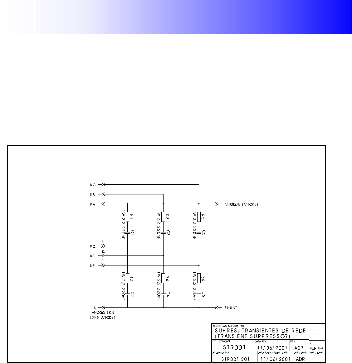
3. +32V power supply transient suppressor:
3.1. Function:
The transient suppressor eliminates the high frequency transients generated by the SCR diodes
fast commutation.
3.2. Technical Description:
The RC circuit that is connected in parallel to the SCR’s from rectifying bridge, is used to
decrease the switching transients, from anode to catode of each SCR.
3.3 Circuit Diagram STR001:
Unit 6 – +32V power supply
- 11 -
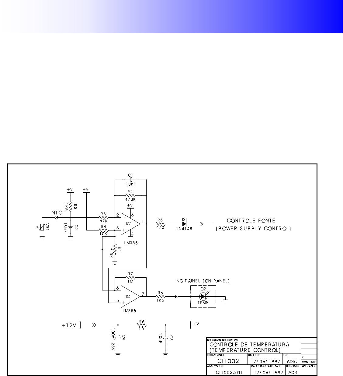
4. Temperature control:
4.1. Function:
Its function is to protect against the power supply temperature increasing.
4.2. Technical Description:
Through a NTC (VR1) thermistor that is set up over the SCR’s heat sink of the three-phase
rectifier bridge, a sample voltage is compared to a reference voltage that is obtained by R4 and trimpot
R1. If the power temperature overcome the value determined trimpot R1, the integrated circuit IC1
output passes to the high level by resistor R5 and diode D1and acts in the control pins from the phase
controller circuits from the three-phase control power board (FTE012), decreasing the SCR’s conducting
angle and consequently reducing the output voltage.
4.3. Circuit Diagram CTT002:
Unit 7 – Cabling and attributes
- 2 -
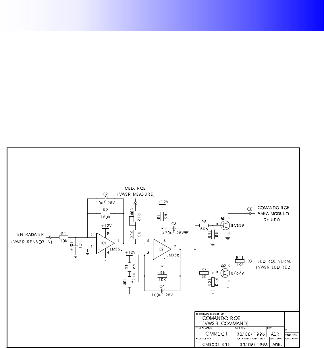
1. VSWR Command:
1.1. Function:
Its function is to protect the equipment if there is an antenna excessive VSWR.
1.2. Technical Description:
The detected sample by the directional coupling is applied to IC1 integrated circuit. IC1 output
is compared to the adjusted reference value by trimpot R13.
If VSWR exceeds the pre-adjusted limit, IC2 integrated circuit output passes to the high level,
conducting transistors Q1 and Q2. Transistor Q2 lights the red Led in the transmitter output power
measurement.
1.3. Circuit Diagram CMR001:
Unit 7 – Cabling and attributes
- 4 -
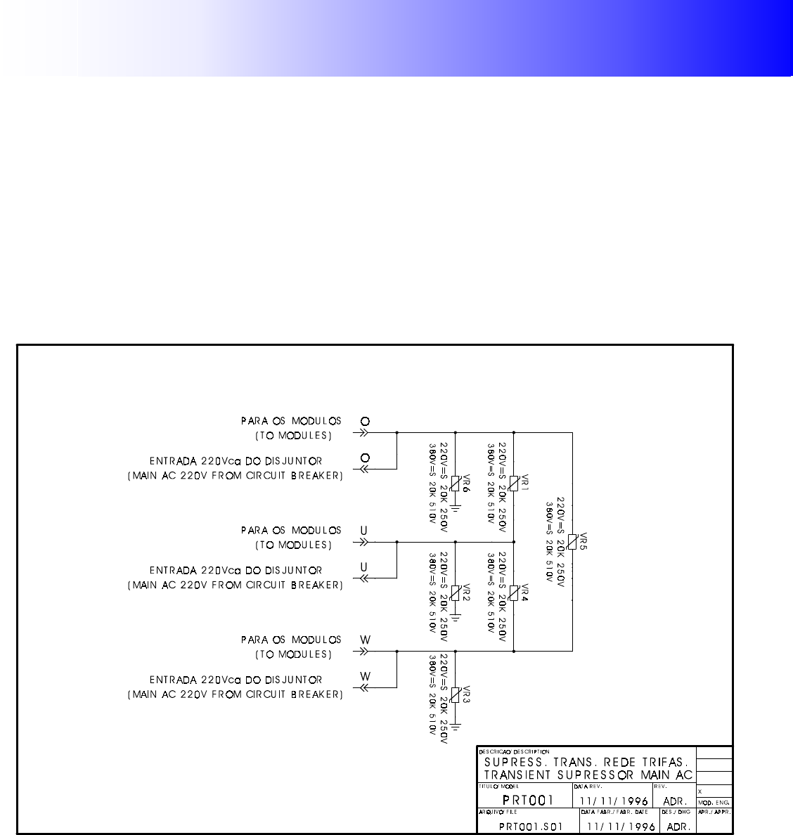
2. Three-phase transient suppressor protection:
2.1 Function:
Its function is to protect against voltage peaks in the three-phase circuit network that occurs
because of atmospheric discharges or transients.
2.2 Technical Description:
This circuit is composed by six varistors: VR1, VR2, VR3, VR4, VR5 and VR6. The varistors VR1,
VR4 and VR5 are interconnected Phase to Phase and the varistors VR2, VR3 and VR6 are connected
Phase to Ground.
2.3. Circuit Diagram PRT001:

Unit 7 – Cabling and attributes
- 6 -
3. TV monitor:
3.1. Function:
The TV monitor function is to detect the output RF signal and final amplifier, providing the video
carrier output power reading and audio carrier and the video signal monitoring that have been
transmitted.
3.2. Technical Description:
The obtained signal through the directional coupler supplies the monitor input, by connector J1.
The resistors R14 and R15 provide 50 Ohm termination for interconnecting cabling. The diodes
D2 and D3 function is to detect the RF signal and they are polarized to a better linearity through R1,
R2, D1, C1 and L1. The linearity adjustment is made by R4.
The detected signal by D2 supplies the detector peak circuit via R4, formed by IC1, IC2A and
associated components in order to obtain the output peak sync power reading from the power stage.
Through R12, the reading is adjusted to the panel. The detected signal by D3, after passes by
Q1, that provides high impedance to D3, it supplies the 4.5 MHz filter formed byL2, C26, C27, C12,
R18 and R19. The filter can be short cut by CH1.
The video signal through trimpot R20, supplies the video IC6 that through R38 shows a 75 Ohm
output impedance.
3.3. Adjustment Procedure:
a) The trimpot R12 is put at half course.
b) The directional coupler detector is adjusted in order to obtain the reading in the meter and
directivity.
c) R20 is adjusted till we obtain video 1Vpp in the oscilloscope that is terminated in 75 Ohm.
d) R35 is adjusted to 0Vdc in the blanking level.
e) Through R2, the video linearity is adjusted.
f ) Through L2 and R18, the filter is syntonized for 4.5 MHz minimum value over the video.
Unit 7 – Cabling and attributes
- 11 -
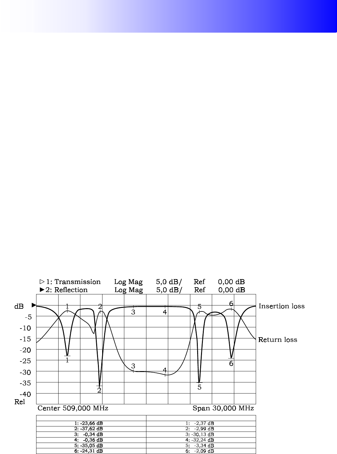
4. Notch filter:
4.1. Function:
Its function is to attenuate the adjacent channel spurious undesirable to the transmitter
operation
4.2. Introduction:
We have in the transistorized equipments, after the final amplifier, besides the desired channel,
spurious of –9, -4.5, +4.5, +9 and sometimes ±13.5 MHz. These spurious usually appear through the
amplification of the output transistor, affecting the adjacent channels.
This filter is able to eliminate the spurious out of band, maintaining only the desired channels.
It is important to remember that there are specifications for these values, which must be
followed.
4.3. Adjustment Procedure:
After the channel information, the filter is adjusted to the NETWORK analyzer, verifying the
return loss and the insertion loss.
This filter is composed of six notch and in this manner they are calibrated as follows:
_ 1 trap to –9.0 MHz
_ 2 traps to –4.5 MHz
_ 2 traps to +4.5 MHz
_ 1 trap to +9.0 MHz
The combination of notches in the Notch filter performs a better return loss and insertion
adjustment, as well as, its distribution causes smaller heating.
4.4. Characteristic Curve at the Network Analyzer:
Unit 7 – Cabling and attributes
- 12 -
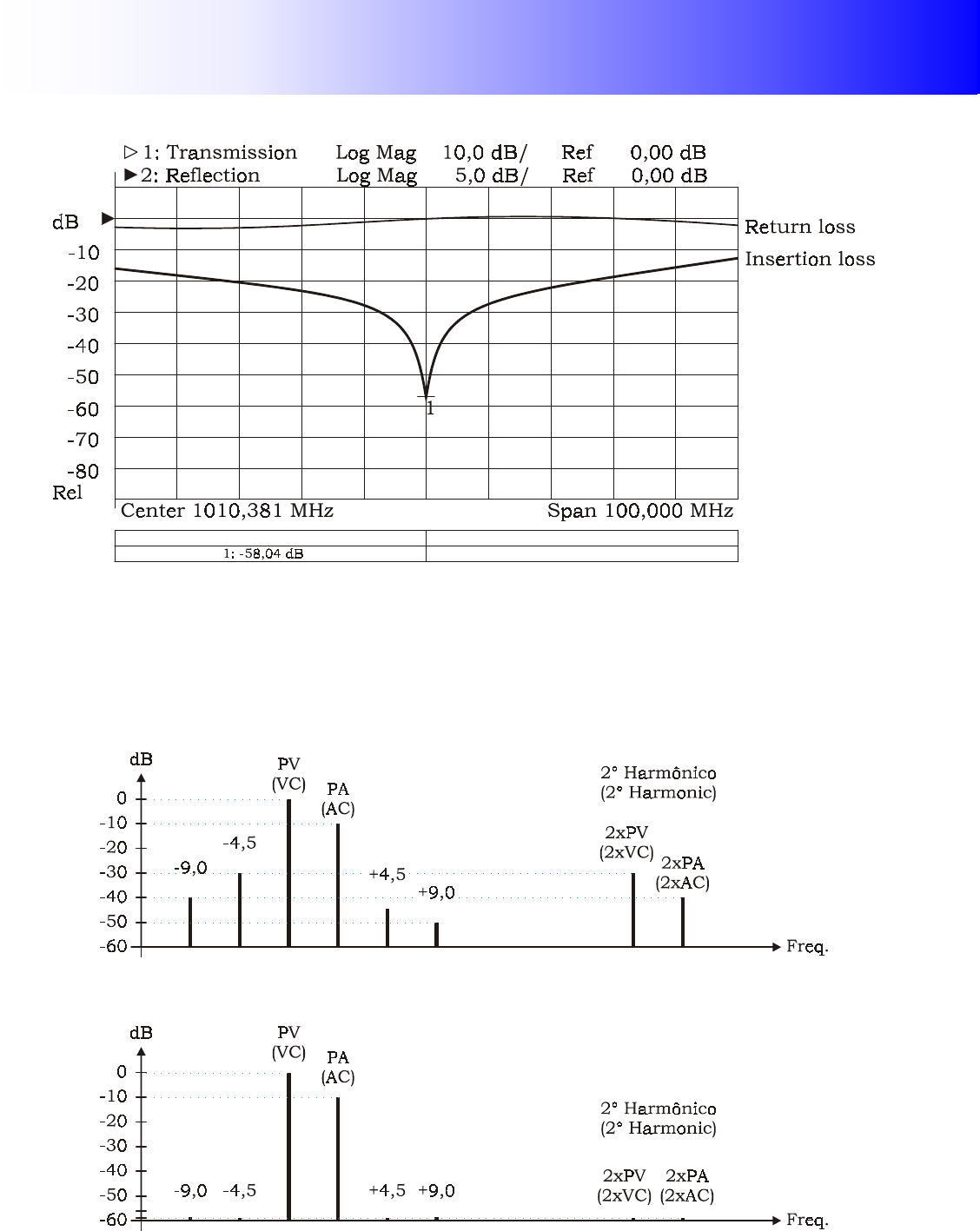
4.5. Characteristic Curve at the Network Analyzer -2° Harmonic:
4.6. In practice
Below there are two RF signal diagrams in the Spectrum Analyzer.
1° without trap filter:
2° with trap filter:
In the second chart the –9.0 MHz spurious should be at least –60dB, regarding to the video
carrier.