Lierda Science and Technology Group LSD1BTNBLE0000 The KW31 BLE Module User Manual
Lierda Science & Technology Group Co.,Ltd The KW31 BLE Module
User Manual
LIERDA Science & Technology GROUP Co., LTD.
Product Specification
Product Name: The KW31 BLE module
Product Model: LSD1BT-NBLE0000
Version: V1.5

Table of Contents
Chapter I: Functional Features ........................................................................................................................... 4
Chapter III: Hardware Layout and Interface Specification ................................................................................ 6
Chapter IV: Application Specification ............................................................................................................... 8
4.1 Module application circuit ................................................................................................................... 8
4.2 Precautions on module usage ............................................................................................................... 9
Chapter V: Functional Specification ................................................................................................................ 10
5.1 Networking function .......................................................................................................................... 10
5.2 Serial port framing mechanism .......................................................................................................... 10
5.3 Transparent transmission mode .......................................................................................................... 11
5.4 Command mode ................................................................................................................................. 11
5.5 Echo mode ......................................................................................................................................... 11
5.6 Serial port upgrade mode ................................................................................................................... 11
5.7 Low power mode ............................................................................................................................... 11
5.9 Service specification .......................................................................................................................... 13
5.10 Serial frame structure ....................................................................................................................... 13
5.11 Serial command overview ................................................................................................................ 14
Chapter VI Work Instruction of Reflow Soldering .......................................................................................... 17
Notes to Users: ................................................................................................................................................. 18

Document Revision Record
Product
Name
The KW31 BLE Module
Product Model
LSD1BT-NBLE0000
Prepared
by Qiu Mangang
Date of
Preparation May 14, 2017
No.
Revision log
Revised
by
Checked
by
Document
Version
Revision
Date
1
Initial version
Qiu
Mangang
V0.1
May 14,
2017
2
Hardware upgrade change leads to I0
port
Qiu
Mangang
V0.2
Jun. 13,
2017
3
Revise user model
Qiu
Mangang
V0.3
Nov
.
6, 2017
4
Update dimension drawing; update
some parameters; update documentation
error; release officially
Qiu
Mangang
V1.4
Apr.
27,
2018
5
Revise module state output I0 port
Huang
Lutong
V1.5
Jun
.
13,2018

Chapter I: Functional Features
LSD1BT-NBLE0000 (The KW31 BLE Module) is a highly integrated low-power Bluetooth module
based on NXP Kinetis KW31Z Soc chip development. Built-in ceramic antenna provides a complete RF
solution without the need for any additional wireless investment to
DFFHOHUDWHSURGXFWGHYHORSPHQW$UP &RUWH[-M0+ 32-bit based processor supports Bluetooth 4.2 to
provide efficient connection. Built-in DC-DC conversion supports 1.8-4.2V wide voltage input to improve
power efficiency. 512K Flash 128K RAM supports a variety of applications for customers. The module
can be widely used in short-range wireless communication fields in various occasions to realize full
transparent transmission. Users can configure various UART data formats according to actual applications
and have the characteristics of small size, low power dissipation, long transmission distance, strong anti-
interference ability, etc., convenient for customers to choose;
The KW31 BLE Module can be widely used in the following occasions:
Ɣ 6PDUWWR\V
Ɣ +HDOWKWHVWLQJ
ƔSmart family;
ƔSafety and security.

Chapter II: Specification Parameters
Table 2 LSD1BT-NBLE0000 module parameters
Parameters Performance Remarks
Operating voltage
1.8V to 4.2V
2.1V requ
ired to startup
Operating
temperature -40 ̚85 ć
Operating frequency
2402~ 2480MHz
Power dissipation
Transmitting
state
P$#9
Typical value: 10.6mA@0dBm CW
Receiving
state
P$#9
Typical value: 11.5mA@MCU RUN
Sleep state
X$#9
VLPS at Buck mode(3.3 V),
Transmitting power
2--3dBm Typical value: 2.5dBm @3.3V CW
Receiving
sensitivity Better than -93 dBm
Typical value:
-90dBm
Channel 40
Channel spacing 2M
Modulation system
GFSK @ 1Mbps
C
ommunication
Protocol BLE
Reliable
transmission
distance
>12m@0dB
Open visual environment, the actual distance is
affected by factors e.g. surrounding
environment, air humidity, etc.
Interface type
Stamp hole patch type
Shield Yes
Dimensions
(length ×
width ×
thickness)
9mm×11.5mm
×2.7mm
The module comes with ceramic antenna
Antenna type
Multilayer Chip Antenna
Antenna gain 0.5dBi
Antenna size
(L*W) 3.2*1.6mm
Remarks:
The actual distance is affected by various factors, e.g. ambient temperature, humidity, bottom plate,
casing, mobile phone, etc. The data is only used for reference and not for guarantee.
Chapter III: Hardware Layout and Interface Specification
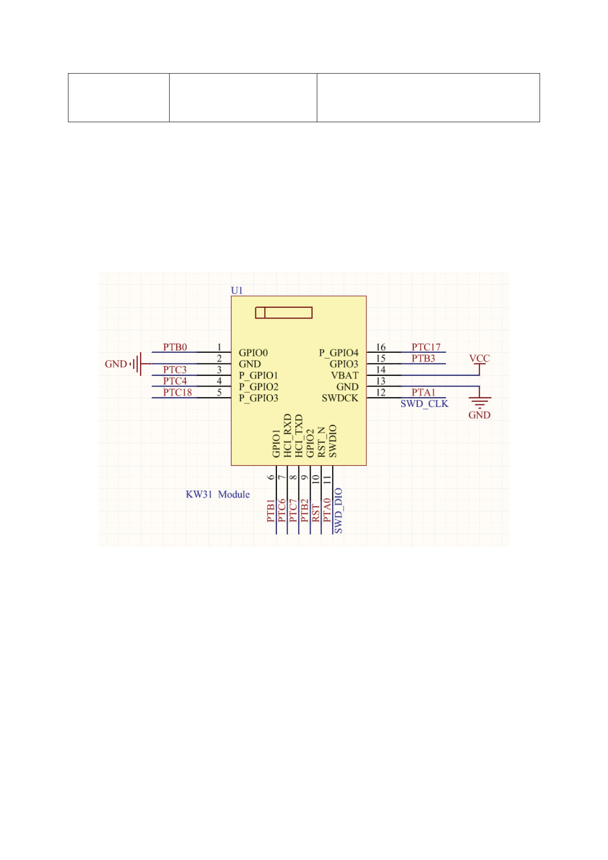
The definition of LSD1BT-NBLE0000 module pin is as shown in figure 1:
Figure 3-1 Definition of LSD1BT-NBLE0000 module pin
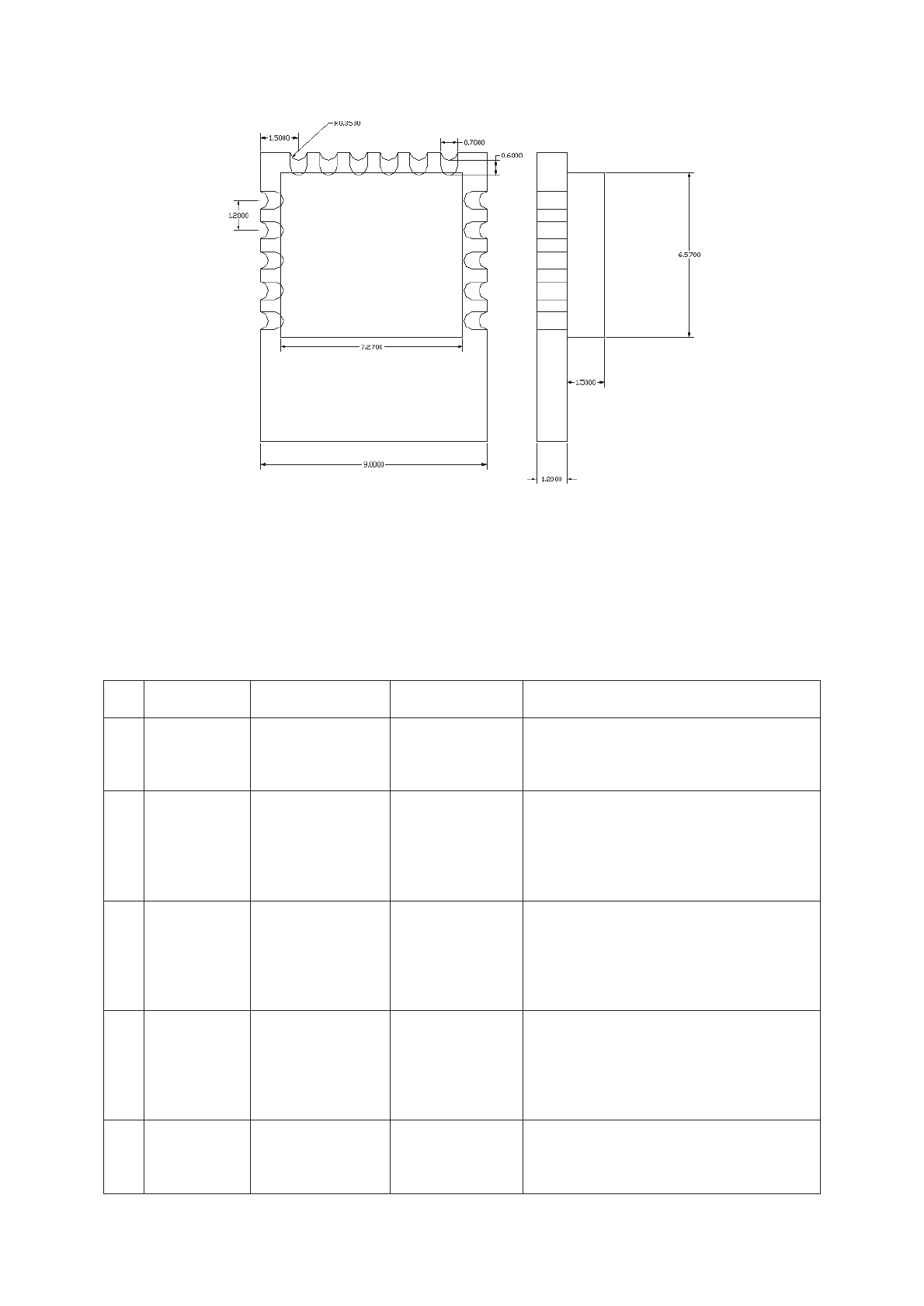
Unit: mm
Figure 3-2 Outline dimension drawing of LSD1BT-NBLE0000 module
Module wrapping is as shown in figure 3-2;
The description of pin function is as shown in figure 3-1.
Table 3-1 Description of LSD1BT-NBLE0000 module pin function
No.
Name
Type
Pin
Explanation
1
GPIO0
GPIO
PTB0
General GPIO, supporting low power
wakeup
2
GND
GND
Necessary
ground
connection
Power ground
3
P_GPIO0
POW_CTRL
(function I/O)
PTC3
Low
-power control pin. Fa
lling edge
enters low power dissipation; rising edge
exits low
-power dissipation
4
GPIO1
BLE transmission
state output
PTC4
High level output during enabling
transmission, low level output during
disabling transmission
5
P_GPIO1
BT_CTRL
(function I/O)
PTC18
Bluetooth broadcast control I/O. Broadcast
at low level, closedown at high level;

6
P_GPIO2
BLE connection
state output
PTB1
Low level in connection state, high level
in disconnection state
7
HCI_RXD
DI
PTC6
UART_RX
8
HCI_TXD
DO
PTC7
UART_TX
9
GPIO2
GPIO
PTB2
General I/O
10
RST_N
RESET
RST(
Active
Low)
Pin reset, low level reset, high level by
default
11
SWDIO
SWD
PTA0
SWD program download interface
12
SWDCK/
P_GPIO3
SWD/module
LED state
PTA1
SWD program download interface;
Flashing 2 times per second in connection
state, flashing once every 3S in
disconnection state.
13
GND
GND
Necessary
ground
connection
Power ground
14
Vbat
POWER
1.8V
²4.2V
Power 3.3V
15
GPIO3
GPIO
PTB3
General GPIO
16
P_GPIO4
PIN_MODE
(function I/O)
PTC17
Command mode selection I/O
Low level CMD, high level DTU
Note: general GPIO is configured by default as floating input.
More pin function descriptions in KW31 latest data book;
http://cache.nxp.com/assets/documents/data/en/data-sheets/MKW41Z512.pdf
Chapter IV: Application Specification
4.1 Module application circuit
Refer to the following circuit for module minimum system
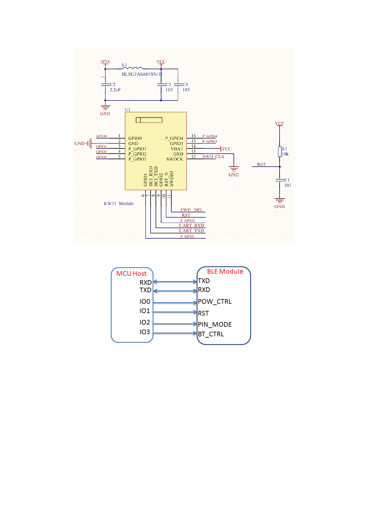
Figure 4-1 Module recommended minimum system
Figure 4-2 Connection between host and module pin
The pins that need to be connected to the host when the module works normally are as shown in
figure 4-2. At least four IO ports are required to control the module. PWR_CTRL refers to low lower
control pin; the falling edge enters power dissipation, while the rising edge exits lower power dissipation.
PIN_MODE refers to command and transparent transmission mode switch; pin low level is the command
mode, while the high level is the transparent transmission mode. BT_CTRL refers to the broadcast control
pin; it enters broadcast state at low level and the broadcast stops at high level.
4.2 Precautions on module usage
In order to ensure that RE performance of module is the most effective in applications, users shall
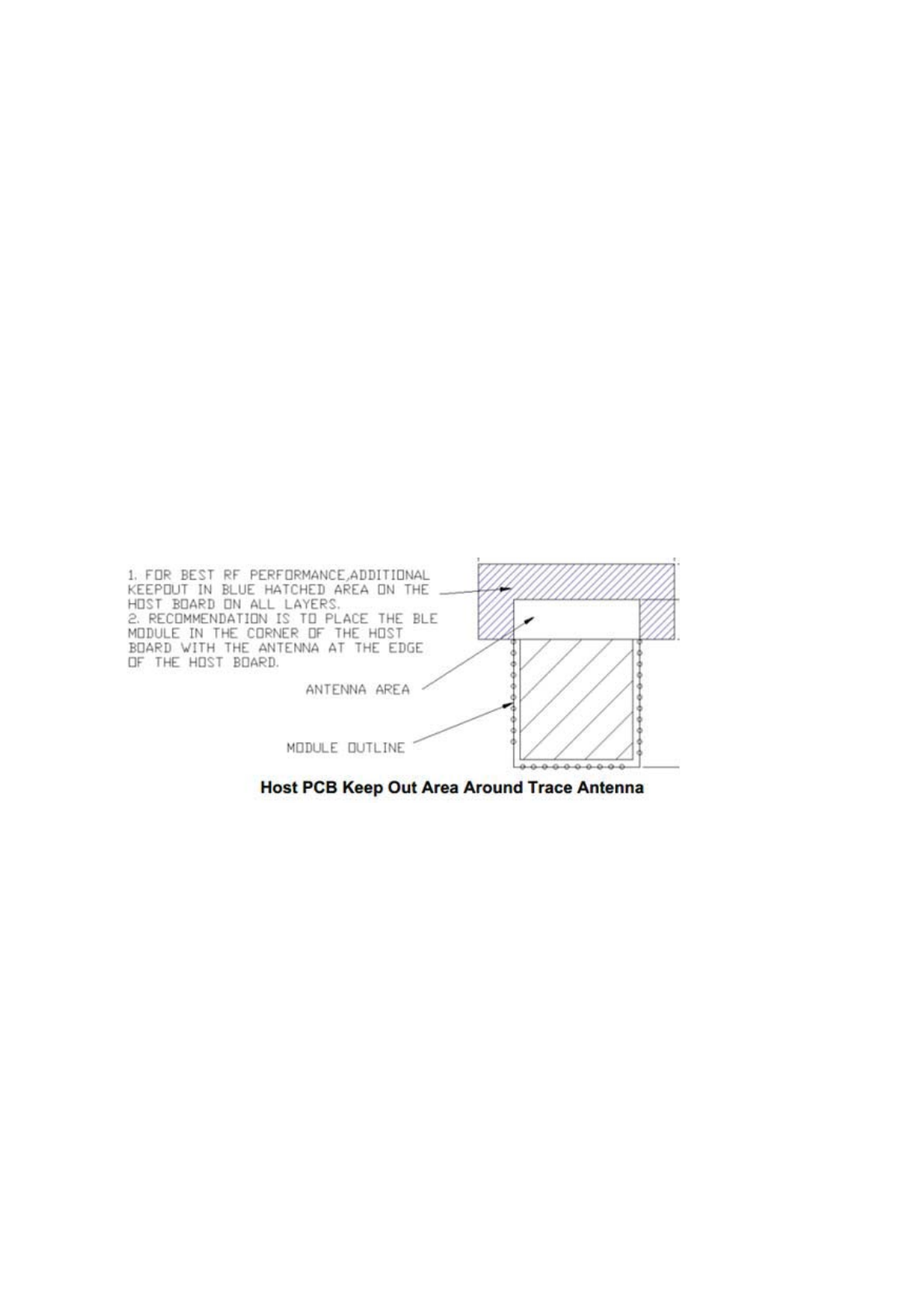
follow the following principles in use:
1. It is recommended to use DC stabilized power supply for the module. Power supply ripple
coefficient shall be as small as possible. The module shall be grounded reliably. Please pay attention to the
connection between positive and negative poles of the power supply. Reverse connection may cause
permanent damage to the module;
2. It is recommended to place the module at the open space of bottom plate edge and the antenna shall
face outwards;
3. PCB board (double-sided board and multi-layer board) below the antenna in the module needs to be
cleaned and cannot be coated with copper, i.e. there shall be no grounding or signal trace for all layout
layers below the antenna;
4. It is best not to have metal devices near the antenna, otherwise the communication distance of
modules will be shortened to varying degrees in different environments.
Figure 4-2 Module PCB layout
Chapter V: Functional Specification
5.1 Networking function
The transparent transmission module is temporarily only used as a slave device to connect to piconet
with master device. The existence of these interfaces not only greatly expand the connection mode of the
module but also can enable users to dock with the modules and realize the network transmission of data;
5.2 Serial port framing mechanism
URAT has a framing mechanism. The continuous transmission is one frame, but the number of bytes
per frame must be less than 1500 bytes. The framing is related to the low power mode. In low power mode,

transparent transmission module will ignore all the data received. The module must be woken up before
data can be set and received.
5.3 Transparent operating mode
Serial port transparent transmission working mode is supported to realize data transfer from wired
serial port to Bluetooth wireless transmission or achieve transparent transmission to serial port through
Bluetooth wireless transmission. Transparent transmission working mode enables products of customers to
achieve the fastest and simplest wireless communication.
UART->APP˖When uart sends data, the length of a packet to be sent needs to be determined by the
transmission interval and the connection interval of modules. The data of one frame cannot exceed 1500
bytes.
APP->UART˖APP needs to be cached. Ble can only send 1500 bytes in one frame (the frame will be
dropped if there are more than 1500 bytes).
5.4 Command mode
Command configuration mode is supported to configure and read the device information of module as
well as the parameters configured by users. See 5-11 serial port command overview for details.
5.5 Echo mode
The module enters echo mode when the module is in unconnected state and PIN_MODE is high. At
this time, the data can be received at HCI_RXD terminal through HCI_TXD printing module to facilitate
debugging by users.
5.6 Serial port upgrade mode
The module supports the serial port online upgrading function. When the module is reset, 16-byte
IRUPDWFRPPDQG³ymodem´LVVHQWWRWKHPRGXOHDWDQ-bit length of 115200 baud rate and one-stop bit
no parity through thH VHULDO SRUW 7KH PRGXOH ZLOO UHWXUQ WR ³&´FKDUDFWHU DIWHU UHFHLYLQJ WKH FRPPDQG
which indicates successful entry into the serial port upgrade mode and waiting to receive the upgrade
program. It will be started according to the new program if the upgrade is successful, otherwise it will be
started from the original program.
5.7 Low power mode
The module enters low power mode when the module POW_CTRL pin is pulled low. At this time, the
module will no longer broadcast or receive the data sent by Bluetooth and the host serial port. It will exit
the low power mode when POW_CTRL pin is pulled high.
5.8 Module mode switching
Table 5-1 Switching of module modes
Mode Entry Mode Exit Mode
Transparent
transmission mode
POW_CTRL works properly for high modules. It
enters transparent transmission mode after
successful Bluetooth pairing
Module disconnection
Command mode
It enters command mode if PIN_MODE is low
Pulling command pin high
Echo mode
Pull PIN_MODE high and the module is not
connected
Module connection or pulling
down command pin
Serial port
upgrading mode
See the IAP documentation for details
Automatically exiting after
the upgrade is complete
d
Low power mode
Pull the PWR_CTRL pin low to enter low power
mode
Pulling the PWR_CTRL pin
high to exit low power mode
In command mode, the users control BLE transparent transmission module through the serial port
command, as shown in figure 5-1. The primary controller sends a command to BLE transparent
transmission module. BLE transparent transmission module will send an acknowledge frame to the
controller MCU after receiving the command and executing it to characterize the result of command
execution.
MCU BLE
UART:CMD
UART:ACK
Figure 5-1 Main controller and BLE transparent transmission module command form
In transparent transmission mode, MCU sends data to the module, and then the module transmits to
the mobile phone through BLE protocol. The mobile phone sends data to the module through BLE
protocol, and then the module sends to MCU through the serial port, as shown in figure 5-2.

MCU PHONEKW31
UART:TX
UART:RX
BLE TX
BLE RX
Figure 5-2 Specification of model transparent transmission
5.9 Service specification
Service Name
UUID
Notes
service_gatt 0x1801
GATT service
service_gap 0x1800
GAP service
service_device_info
0x180A
Equipment information service
service_battery
0x180F
Battery service
service_dtu
0xE0, 0x1C, 0x4B, 0x5E, 0x1E, 0xEB, 0xA1,
0x5C, 0xEE, 0xF4, 0x5E, 0xBA, 0xE7, 0xFE,
0xFF, 0x01
Universal transparent
transmission service
5.10 Serial frame structure
The commands of transparent transmission module have a certain format, including five areas of
³KHDGHU´³FRPPDQG,'´³FRPPDQGLQIRUPDWLRQOHQJWK´DQG³FRPPDQGLQIRUPDWLRQ´
The details are as follows:
Input command format (hex)
Header
header
Command ID
Message length
Message Content
01 FC XX XX
;;«;;
Output response format (hex)
Header
Header
Command ID
Message Length
Message Content
04 FC XX XX
;;«;;
Header: in order to ensure that the input command can be correctly parsed, all input command frames
muVW VWDUW ZLWK SUHIL[³ )&´ $OO RXWSXW UHVSRQVH IUDPHV VWDUW ZLWK³)&´ZKLFKKHOSVWKHXVHUWR
distinguish command from data.
Command ID: command ID is an identifier between different commands. Different commands have
unique command ID, which are described in detail below.

Message length: message length refers to the number of bytes of message content, excluding prefix,
command ID and message length itself.
Information content: the information content of input command is some input parameters of the
command execution, while the information content of output response is the result of command execution,
which is described in details below.
5.11 Serial command overview
Table 5-2 is detailed specification of output response frame.
Table 5-2 Output response frame format specification
No.
Command ID
Specification
1
01
Correct command, without additional data, return 04 FC 01 00
2
XX
Correct command, with additional data, return 04 FC xx (corresponding to
command ID) xx
(message length) xx...(message content)
3
02
Command error, return 04 FC 02 00
The Bluetooth 4.2 protocol specifies that the pairing password is of 6 digits.
Table 5-3 refers to the detailed description of input command frame.
Table 5-3 Input command frame explanation
Power-
down
Saving
Com
mand
ID
Command
Description
Default
Command Format Return Value
Yes
01
Set baud
rate
115200
01 FC 01 04 XX XX XX XX (uint32,
low endian)
The baud rate unit is bps. The range is
230400~1200. It is transmitted in low
byte rate,
f
or example, for baud rate
115200, the hexadecimal is
0x0001C200, which shall be written as
00 C2 01 00
04 FC 01 00 Correct setu
p
04 FC 02 00
Setup error
/
02
Query baud
rate
/
01 FC 02 00
04 FC 02 04 XX XX XX XX
(uint32, low endian, the same as
ID:01)
04 FC 02 00 false command
Yes
03
Set
connection
0x0028
10ms
01 FC 03 02 XX XX (uint16, low
endian)
04 FC 01 00 Correct setup
04 FC 02 00 Setup error

LQWHUYDO 7KH XQLW RI %OXHWRRWK FRQQHFWLRQ
LV PV 7KH VFRSH LV
[a[LHPVaV
4XHU\
FRQQHFWLRQ
LQWHUYDO
)&
)& ;; ;; XLQW ORZ
HQGLDQWKHVDPHDV
,')& )DOVH
FRPPDQG
<HV 3DLULQJ
SDVVZRUG
)&;;;;;;;;;;
;;XQLWORZHQGLDQ
;; UDQJH a HLJKWGLJLW
SDVVZRUG GHIDXOW
(J)&
7KH PD[LPXP QXPEHU RI
SDLULQJ SDVVZRUG GLJLWV GHILQHG
E\ %/( VSHFLILFDWLRQLV
VXSSRUWHG
)& &RUUHFWVHWXS
)& )DOVH
FRPPDQG
4XHU\
SDLULQJ
SDVVZRUG
)&
)& ;; ;; ;; ;;
;; ;;XLQW ORZ HQGLDQWKH
VDPH DV ,'
)& )DOVHFRPPDQG
4XHU\0$&
DGGUHVV
/RFDO
PDVWHU
0$;
)&
)& ;; E\WHV
0$& DGGUHVVORZHQGLDQ
)& )DOVHFRPPDQG
<HV
6HW
HTXLSPHQW
QDPH
)&;;<<
;;QDPHOHQJWK
<<E\WHGHYLFHQDPH
7KH QDPH OHQJWK PXVW EH WKH
VDPH DVWKHQXPEHURIQDPHE\WHV
)& &RUUHFW
VHWXS)& 6HWXS
HUURU
4XHU\
HTXLSPHQW
QDPH
)&
)& ;; QDPH
OHQJWK <<E\WHQDPH
)& )DOVHFRPPDQG
<HV &
6HW
EURDGFDVW
LQWHUYDO
[
PV
)& & ;; ;;XLQW ORZ
HQGLDQ WKH XQLW RI %OXHWRRWK
EURDGFDVW LV ȝV WKH UDQJH LV
PVaV
)& &RUUHFW
VHWXS)& 6HWXS
HUURU
'
4XHU\
EURDGFDVW
LQWHUYDO
)&'
)& ' ;; ;; XLQW
ORZE\WHWKHVDPHDV,'&
)& )DOVHFRPPDQG
<HV
6HW,2
LQSXW DQG
RXWSXWVWDWH
$OO,2
LQLWLDO
RXWSXWORZ
OHYHO
)& ;; ;; ;;
;; LQGLFDWHV VHOHFWLRQ RI ,2
;; LQSXW RXWSXWVWDWH;;RXWSXW
OHYHO 7KH a E\WHV RI ;;
UHVSHFWLYHO\ LQGLFDWHPRGXOH
7KH a E\WHV RI ;; FRUUHVSRQG
*3,2a*3,2LQSXWRXWSXWVWDWH
7KH a E\WHV RI ;; FRUUHVSRQG
WR
)& &RUUHFW
VHWXS)& 6HWXS
HUURU

GPIO0~GPIO3 output level.
/
11
Query I/O
input and
output state
Yes
12
Read I/O
state
01 FC 14 02 XX (XX respectively
indicate t
hat corresponding I/O
state is read)
/
80
Restore
factory
settings and
restart to
take effect
/
01 FC 80 00
04 FC 01 00 Correct setup
04 FC 02 00 Setup error
/
81
Reset
module
/
01 FC 81 00
04 FC 01 00 Correct setup
04 FC 02 00 Setup error
/
F0
Firmware
version No.
query
/
01 FC F0 00
04 FC F0 02 XX (hardware version)
YY
(firmware version)
04 FC 02 00 Setup error

Notes to Users:
1. Welcome to use the products of LIERDA Science & Technology GROUP Co., LTD. Please read the
notes before using our products. If you have started using, it indicates that you have read and accepted the
notes.
2. LIERDA Science & Technology GROUP Co., LTD. reserves the final right to interpret and revise
all the materials provided.
Prepared by: Microcontroller Business Division of LIERDA Science & Technology GROUP Co.,
LTD .
April, 2018
FCC Statement
Any Changes or modifications not expressly approved by the party responsible for compliance
could void the user’s authority to operate the equipment.
This device complies with part 15 of the FCC Rules. Operation is subject to the following two
conditions:
(1) This device may not cause harmful interference, and
(2) This device must accept any interference received, including interference that may cause
undesired operation.
FCC Radiation Exposure Statement:
This equipment complies with FCC radiation exposure limits set forth for an
uncontrolled environment .This equipment should be installed and operated with
minimum distance 20cm between the radiator& your body.
FCC Label Instructions:
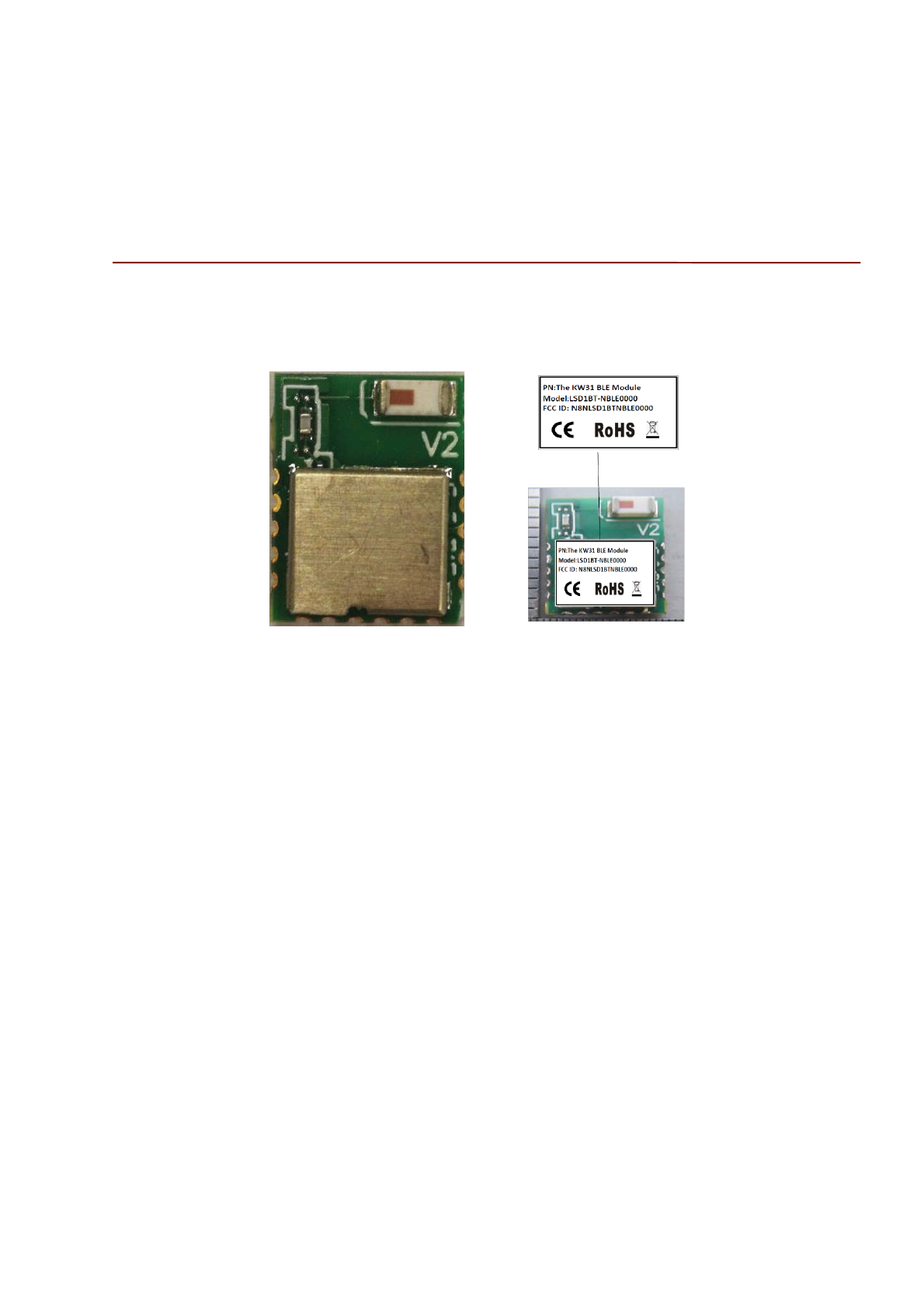
The outside of final products that contains this module device must display a label
referring to the enclosed module. This exterior label can use wording such as: “Contains
Transmitter Module FCC ID: N8NLSD1BTNBLE0000”,or “Contains
FCC ID: N8NLSD1BTNBLE0000 ”, Any similar wording that expresses the same
meaning may be used.