Lierda Science and Technology Group LSD4WF2MD05102 Wifi Module User Manual
Lierda Science & Technology Group Co.,Ltd Wifi Module
User Manual
Company address: No.1326 wenyi west road,Hangzhou,P.R.China Tel:0571-88800000 Fax:0571-89908080
LSD Science & Technology Co., LTD.
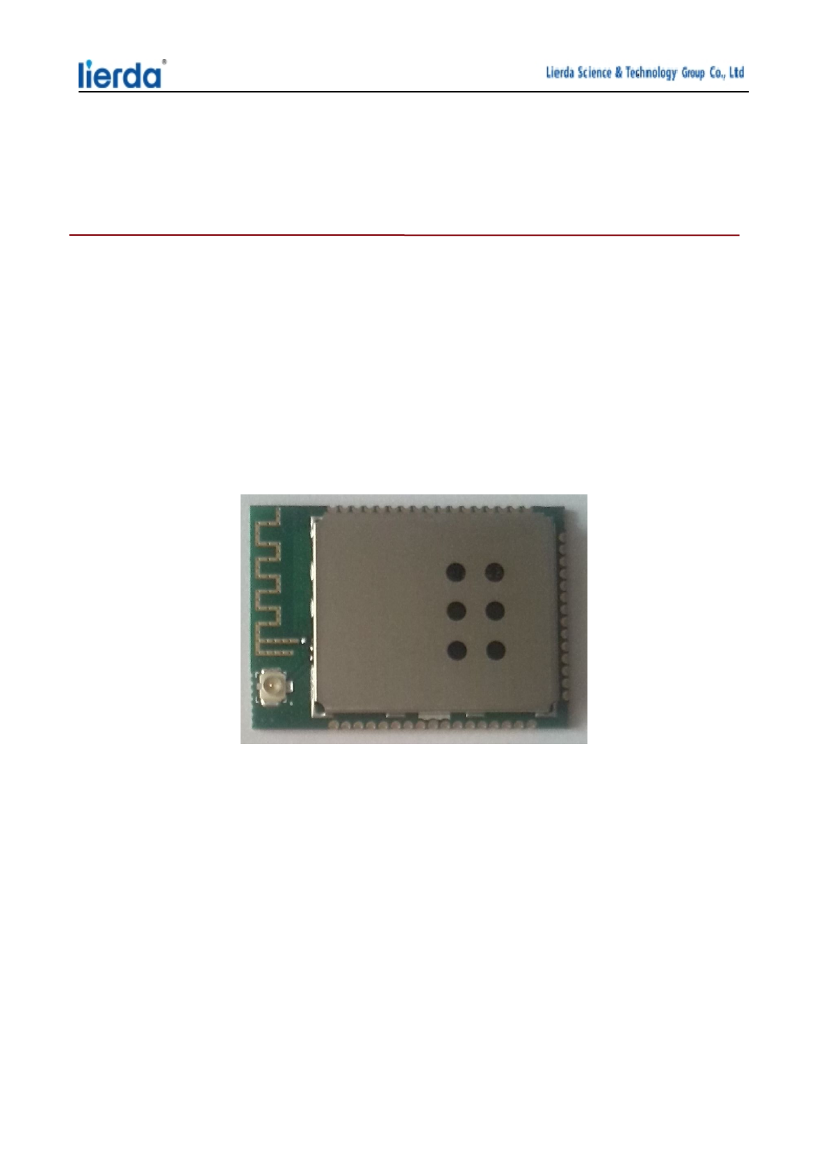
LSD4WF-2MD05102
WiFi Module Date Sheet
Product Name:WiFi Module
Product Type:LSD4WF-2MD05102
File Version: V1.4
Company address: No.1326 wenyi west road,Hangzhou,P.R.China Tel:0571-88800000 Fax:0571-89908080
Version Number Revision Content Data
V1.0 First Release 31.07.15
V1.1 Working temperature range
correction:add furnace
temperature curve
24.09.15
V1.2 Update size chart,company
address
08.10.15
V1.4 Add electric current
parameter
06.05.16
Company address: No.1326 wenyi west road,Hangzhou,P.R.China Tel:0571-88800000 Fax:0571-89908080
Preface
Thank you for using the Wi-Fi Module provided by LSD Science & Technology Co., LTD.
Please read this data sheet carefully before using.The company is not responsible for the property or
personal injury wich was caused by custemor improper operation. Please read the technical
specifications in data sheet for reference during product reserch and development.Before the
declaration,the company has the right to modify the data sheet according to the need to
development.
Copyright:
The copyright of this data sheet belongs to LSD Science & Technology Co., LTD. Any copy
or modify without written consent from LSD will assume legal liability.

Company address: No.1326 wenyi west road,Hangzhou,P.R.China Tel:0571-88800000 Fax:0571-89908080
Catalog
1 Product introduction.............................................................................................................................................. - 5 -
1.1 Product overview........................................................................................................................................- 5 -
1.2 Functional Characteristics.......................................................................................................................... - 5 -
1.3 Application Area.........................................................................................................................................- 5 -
1.4 Structure diagram....................................................................................................................................... - 6 -
2 Module Parameters................................................................................................................................................ - 6 -
2.1 WiFi Features..............................................................................................................................................- 6 -
2.2 Electrical Characteristics............................................................................................................................- 7 -
2.3 Temperature Characteristics....................................................................................................................... - 7 -
3 Hardware structure................................................................................................................................................ - 8 -
3.1 Product size.................................................................................................................................................- 8 -
3.2 Pin definition.............................................................................................................................................. - 8 -
3.3 Label specification....................................................................................................................................- 10 -
4 Application reference...........................................................................................................................................- 10 -
4.1 Reference design...................................................................................................................................... - 10 -
4.2 Module secondary welding reference tempetrature curve....................................................................... - 12 -
5 Packaging.............................................................................................................................................................- 12 -
5.1 Outer carton.............................................................................................................................................. - 12 -
5.2 Inner box...................................................................................................................................................- 13 -
5.3 Tape & reel............................................................................................................................................... - 14 -

Company address: No.1326 wenyi west road,Hangzhou,P.R.China Tel:0571-88800000 Fax:0571-89908080
1 Product introduction
1.1 Product overview
LSD4WF-2MD05102 is a highly integrated WiFi single chip module,it support 150Mbps
physical layer transmission rate.It is full compliance with IEEE 802.11n and 802.11b/g standards.It
provide excellent standard and transmission area, and also porvide feature-rich wireless
connectivity solutions.
The optimized RF architecture and baseband algorithm can provide excellent RF performance
and low power consumption performance.The integrated MAC design could be configured to an
efficient DMA engine and hardware data processing unit.
LSD4WF-2MD05102 provide standard basic function in safety area,service quality and
international standards. It also provide good performance for terminal users in variety of
applications.
1.2 Function Characteristics
● Support IEEE802.11 b/g/n client
● Integrated ARM-CM3 microchip
● Integrated MAC,Multi IO,highly integrated RF architecture
● 1T1R mode support 150Mbps physical layer transmission rate
● Out stamp holes connection
● Support transparent mode and test mode
● Support WiFi direct connection
● Transmission power control in every packet
● Include PCB antenna and external antenna interface
● Integrated MCU,support customized firmware and function
1.3 Application Area
● Smart home,Smart appliance
● Electronic product with network function:E-book,printer,digital photo frame
Company address: No.1326 wenyi west road,Hangzhou,P.R.China Tel:0571-88800000 Fax:0571-89908080
● Industrial remote sensing,telemetry communication
● Home wireless security,the monitoring platform,equipment room power supply,wireless
remote control alarm system for fan device.
● Personal navigation device,set-top box GPS
● POS system,PDA and other wireless intelligent terminal,medical instrument.
● The electronic bus stop board,intelligent traffic dispatching system.
1.4 Structure diagram
Figure 1 structure diagram
2 Module Parameters
2.1 WiFi Features
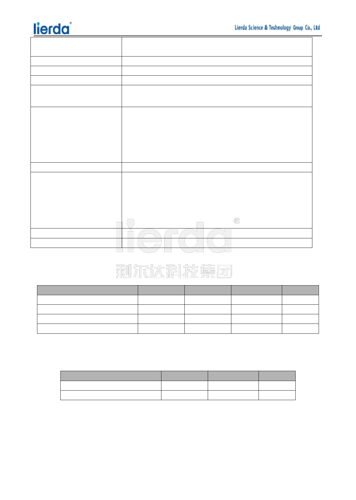
Parameter Specification
Interface Stamp interface
WLANs Accord with IEEE 802.11b/g/n
Modulation Mode 802.11g/n---OFDM(BPSK,QPSK,16QAM,64QAM)
Company address: No.1326 wenyi west road,Hangzhou,P.R.China Tel:0571-88800000 Fax:0571-89908080
802.11b---CCK 11Mbps,5.5Mbp,QPSK 2Mbps ,BPSK
1Mbps
Frequency range 2.4GHz WiFi Band
Operation frequency 2.4GHz
Frequency error < ±25ppm @room temperature +25℃
Operation channel 2.4GHz
RF Power
Antenna PCB Plate antenna(defult),External IPX antenna
Acceptance sensitivity
-85dBm (Typ)@ 11M(802.11b CCK,8% PER)
-73dBm (Typ)@ 54M(802.11g OFDM,10% PER)
-68dBm (Typ)@ MCS7(802.11n OFDM with 20MHz ,10%
PER)
-64dBm (Typ)@ MCS7(802.11n OFDM with 40MHz ,10%
PER)
Humidity 20%-90% non-condensing
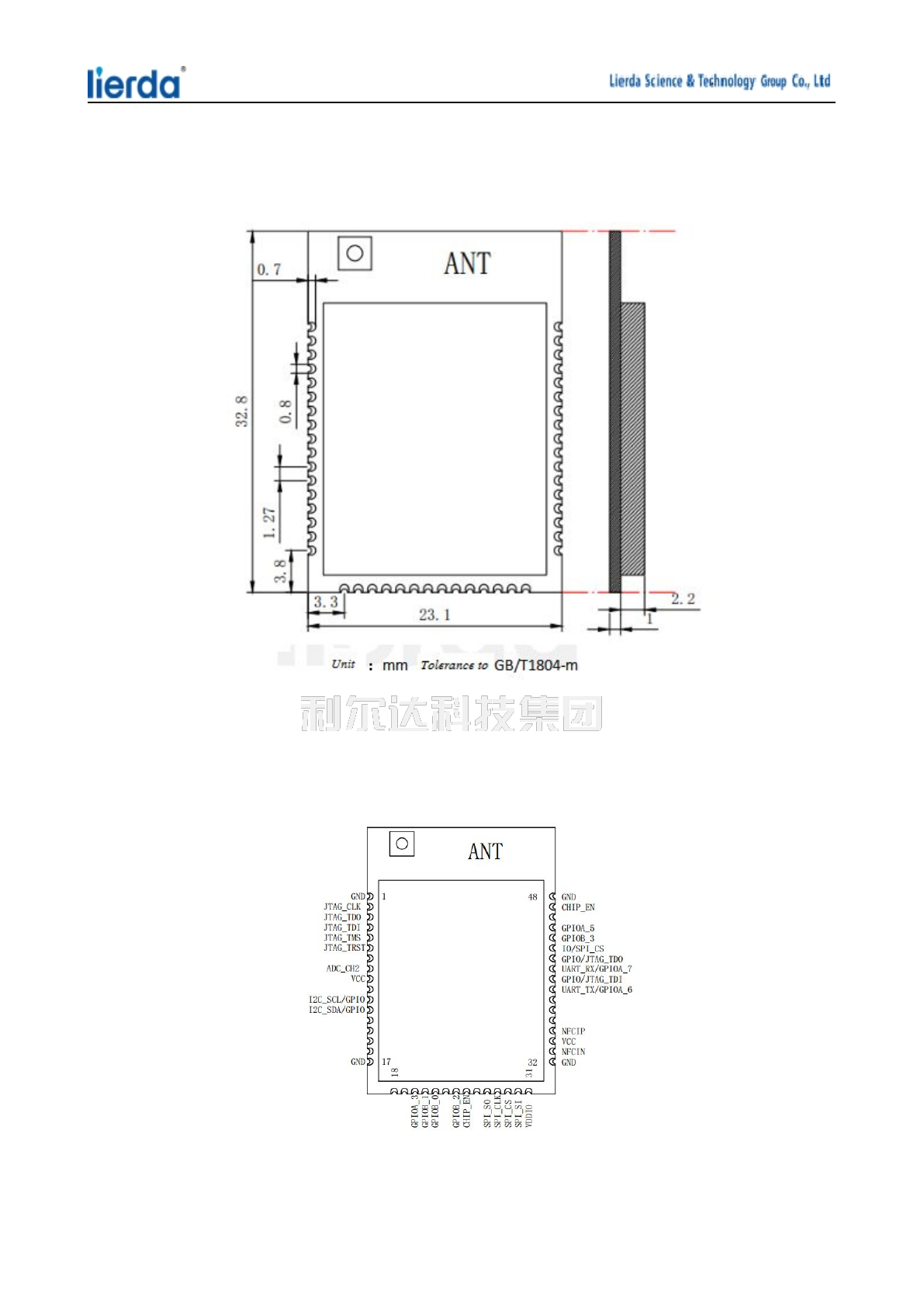
Size (W)23.1×(L)32.8×(H)3.2mm
2.2 Electrical Characteristics
Parameter Minimum Typical Maximum Unit
Working Voltage 3.0 3.3 3.6 V
Quiescent Current / 20 / mA
TX Current / 250 / mA
RX Current / 70 / mA
2.3 Temperature Characteristics
Parameter Minimum Maximum Unit
Working Temperature -20 ℃
Storage Temperature ℃
802.11 b/g/n:2412-2462MHz
14.3-15.9dBm (820.11 CCK,11Mbps)
12.8-13.5dBm (820.11 OFDM,54Mbps)
11.2-11.6dBm (820.11 HT40,MCS7)
13.0-13.7dBm (820.11 HT20,MCS7)
40
-20 40
802.11 b/g/n20:1-11CH
802.11 n40:3-9 CH
Company address: No.1326 wenyi west road,Hangzhou,P.R.China Tel:0571-88800000 Fax:0571-89908080
3 Hardware structure
3.1 Product size
Figure 2 Module size chart
3.2 Pin definition
Figure 3 Module pin funtion diagram

Company address: No.1326 wenyi west road,Hangzhou,P.R.China Tel:0571-88800000 Fax:0571-89908080
Pin Definition Function
1 GND Ground pin
2 jtag_clk/gpio JTAG/IO Multiplexing port
3 jtag_tdo/pwm3 JTAG/IO Multiplexing port
4 jtag_tdi/pwm1 JTAG/IO Multiplexing port
5 jtag_tms/pcm0_in JTAG/IO Multiplexing port
6 jtag_trst/pwm0 JTAG/IO Multiplexing port
8 ADC_CH2 ADC Sampling pin
9 VCC Power supply(DC_3.3V)
11 I2C1_SCL/GPIO I2C/IOMultiplexing port
12 I2C1_SDA/GPIO I2C/IOMultiplexing port
17 GND Ground pin
20 GPIOA_3 IO Port
21 GPIOB_1 Module internal debugging pin(Suspended)
22 GPIOB_0 Module internal debugging pin(Suspended)
24 GPIOB_2 IC Working mode selection(Suspended)
25 CHIP_EN IC Enable pin
27 spi0_so /pwm3 SPI/PWM Multiplexing port
28 spi0_clk/pwm1 SPI/PWM Multiplexing port
29 spi0_cs/pwm0 SPI/PWM Multiplexing port
30 spi0_si/pwm2 SPI/PWM Multiplexing port
31 VDDIO Power supply(DC_3.3V)
32 GND Ground pin
33 NFCIN_1 NFC Function pin
34 VCC Power supply(DC_3.3V)
35 NFCIP_1 NFC Function pin
39 UART_TX/GPIOA_6 UART port/IO port
40 GPIO/JTAG_TDI IO/JTAG Multiplexing port
41 UART_RX/GPIOA_7 UART port/IO port
42 GPIO/JTAG_TDO IO/JTAG Multiplexing port
43 IO/SPI_CS IO 口/SPI Multiplexing port
44 GPIOB_3 IO port
45 GPIOA_5 IO port
47 CHIP_EN IC Enable pin
48 GND Ground pin
Company address: No.1326 wenyi west road,Hangzhou,P.R.China Tel:0571-88800000 Fax:0571-89908080
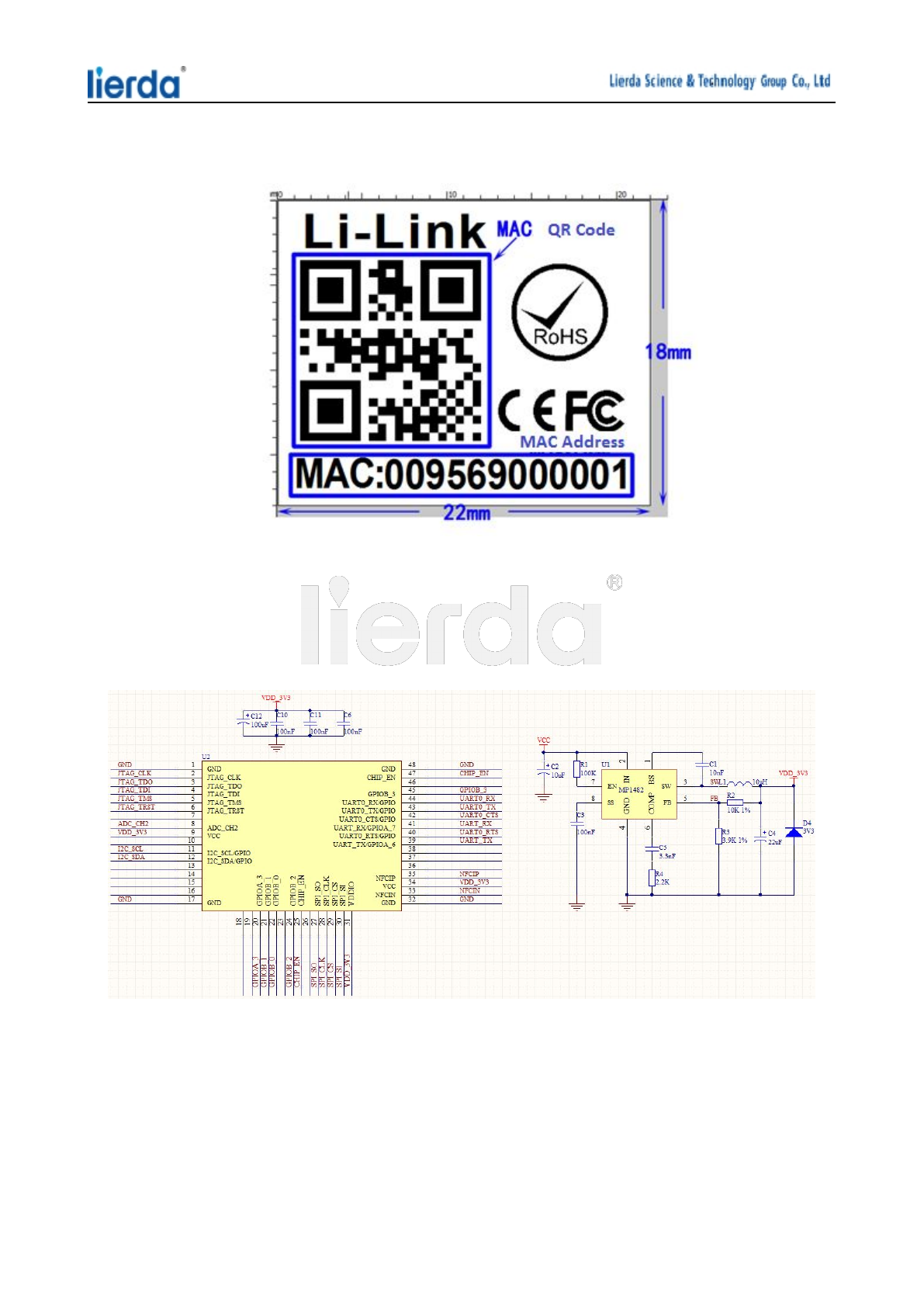
3.3 Label specification
Figure 4 Label instructions
4 Application reference
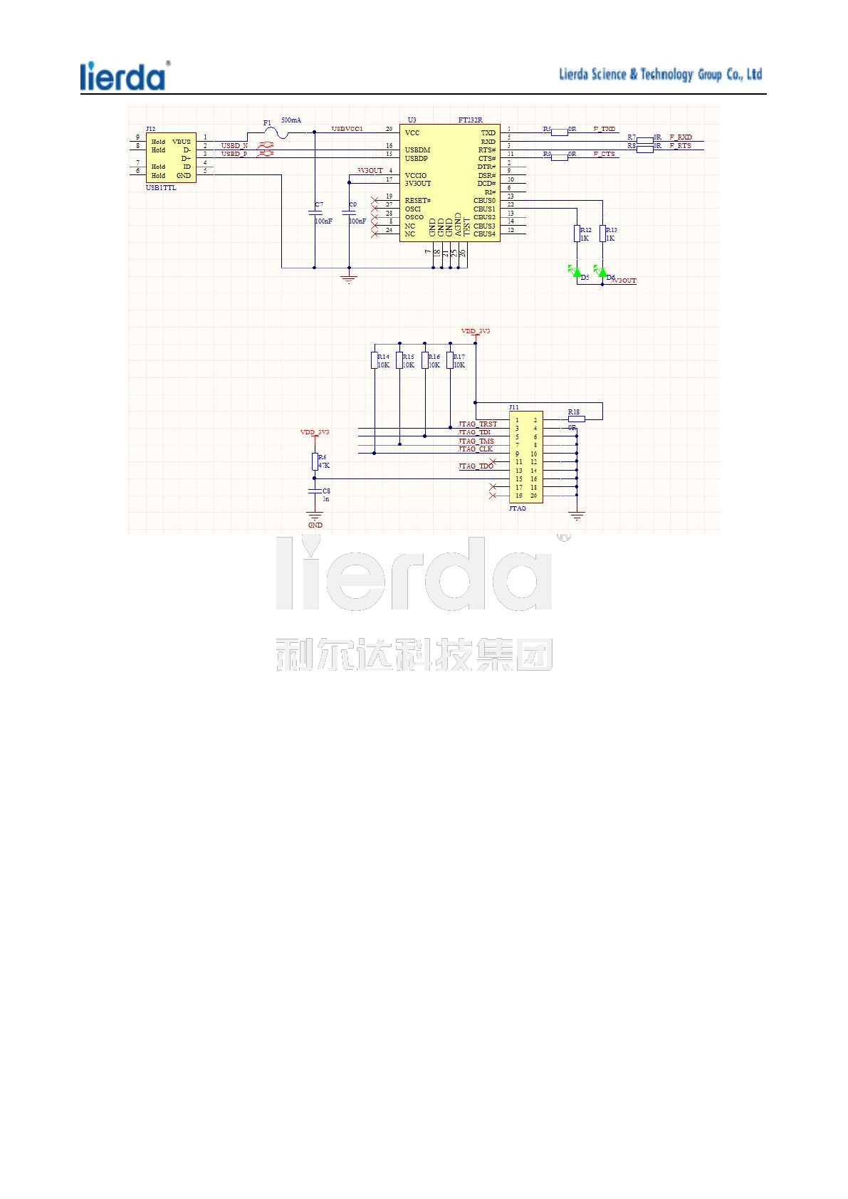
4.1 Reference design
Company address: No.1326 wenyi west road,Hangzhou,P.R.China Tel:0571-88800000 Fax:0571-89908080
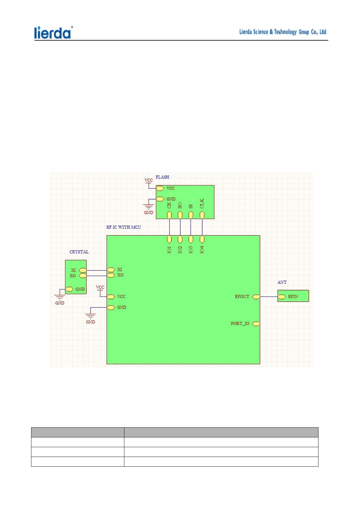
Figure 5 Reference design
Remarks: recommended DCDC Power chip,supply current is greater than 800mA
Company address: No.1326 wenyi west road,Hangzhou,P.R.China Tel:0571-88800000 Fax:0571-89908080
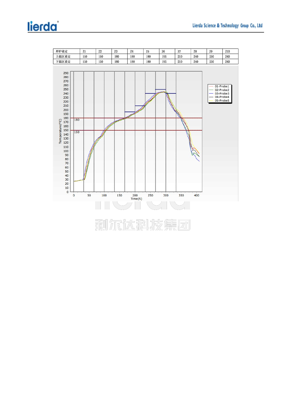
4.2 Module secondary welding reference tempetrature curve
Figure 6 Reference temperature curve
5 Packaging
5.1 Outer carton
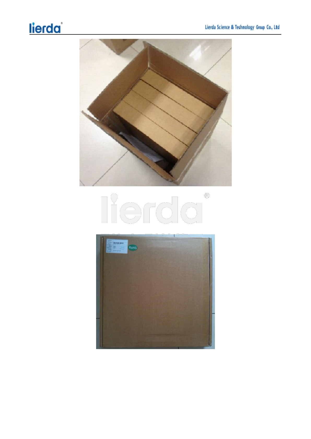
Using outer carton by the size of 354*250*362mm,include inner box.
Company address: No.1326 wenyi west road,Hangzhou,P.R.China Tel:0571-88800000 Fax:0571-89908080
Figure 7 Outer carton assembly drawing
5.2 Inner box
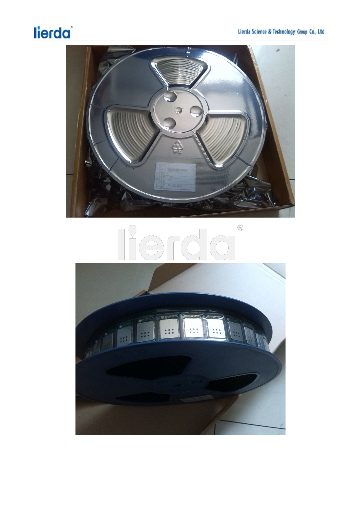
The inner box size is 352*348*56mm,every box contained a tape evacuated with an antistatic
bag,which also contained 500pcs module.
Figure 8 Inner box
Company address: No.1326 wenyi west road,Hangzhou,P.R.China Tel:0571-88800000 Fax:0571-89908080
Figure 9 Evacuated tape with antistatic bag
5.3 Tape & reel
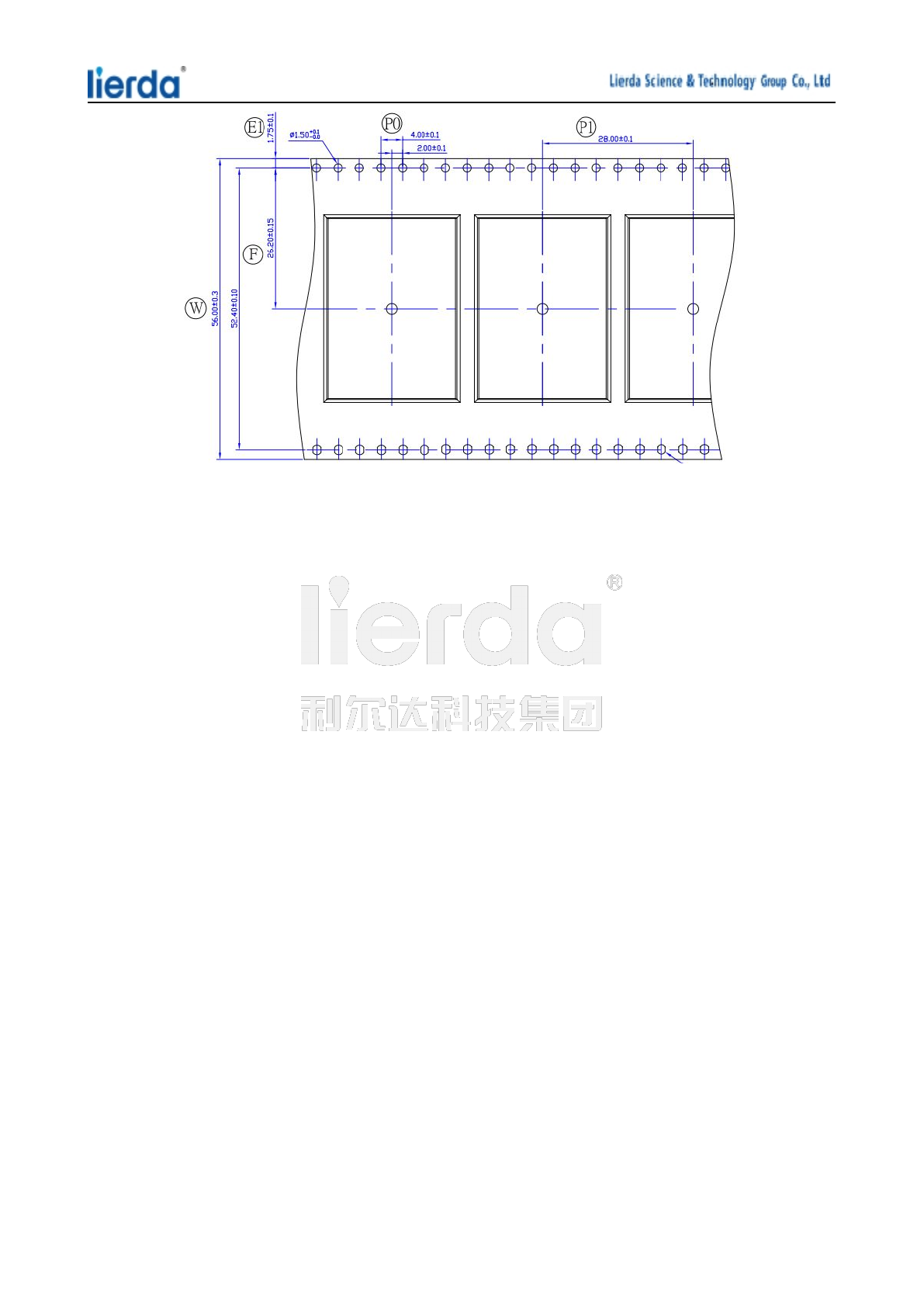
Every tape contained 500pcs module.
Figure 10 Rolling wheel
Company address: No.1326 wenyi west road,Hangzhou,P.R.China Tel:0571-88800000 Fax:0571-89908080
Figure 11 Tape size

1
Maintenance
1.Power rating: Input DC3.3V
2.Declaration of Conformity
Lierda Science & Technology Group Co., Ltd hereby declares that this Wifi Module is in
compliance with the essential requirements and other relevant provisions of Directive
1999/5/EC.a copy of the original declaration of conformity may be found or obtained at
http://www.lierda.com/
FCC Caution.
This device complies with part 15 of the FCC Rules. Operation is subject to the
following two conditions: (1) This device may not cause harmful interference, and (2)
this device must accept any interference received, including interference that may
cause undesired operation.
Any Changes or modifications not expressly approved by the party responsible for
compliance could void the user's authority to operate the equipment.
Note: This equipment has been tested and found to comply with the limits for a Class B
digital device, pursuant to part 15 of the FCC Rules. These limits are designed to
provide reasonable protection against harmful interference in a residential installation.
This equipment generates uses and can radiate radio frequency energy and, if not
installed and used in accordance with the instructions, may cause harmful interference
to radio communications. However, there is no guarantee that interference will not
occur in a particular installation. If this equipment does cause harmful interference to
radio or television reception, which can be determined by turning the equipment off
and on, the user is encouraged to try to correct the interference by one or more of the
following measures:
-Reorient or relocate the receiving antenna.
-Increase the separation between the equipment and receiver.
-Connect the equipment into an outlet on a circuit different from that to which the
receiver is connected.
-Consult the dealer or an experienced radio/TV technician for help.
The distance between user and device should be no less than 20cm.
The Wifi module is designed to comply with the FCC statement. FCC ID is
N8NLSD4WF2MD05102. The host system using Wifi module, should have label
indicated it contain modular’s FCC ID N8NLSD4WF2MD05102.