Lierda Science and Technology Group LSD4WF2MD05106 Wi-Fi Module User Manual
Lierda Science & Technology Group Co.,Ltd Wi-Fi Module
User Manual
1
Lierda Science & Technology Ltd
LSDSCIENCE&TECHNOLOGYCO.,LTD.
LSD4WF-2MD05106(XXXY)
Low Power Wi-Fi Module User Manual
Model :LSD4WF-2MD05106
Name :Wi-Fi Module
Revision :v1.0

2
Index
1.Productoverview .............................................................................................................................................. 3
1.1GeneralDescription ................................................................................................................................ 3
1.2Features ..................................................................................................................................................... 3
2.Parameters .......................................................................................................................................................... 4
3.Package ................................................................................................................................................................ 5
4.Pindefinition ...................................................................................................................................................... 6
5.Behaviorofelectricity ....................................................................................................................................... 8
6.Typicalapplication ............................................................................................................................................ 8
7.Referencedesign ............................................................................................................................................... 9
8.Developingtool ................................................................................................................................................. 9
OEM Labeling Requirements:
NOTICE:The OEM or final integrator must ensure that FCC labeling requirements are
met.This includes an additional label on the outside of the final product housing
with the following contents:
Company Name:XXXX
MODEL: YYYY
Contains Model: LSD4WF-2MD05106(XXXXY) FCC ID:N8NLSD4WF2MD05106
This device complies with part 15 of the FCC Rules. Operation is subject to the following two
conditions: (1) This device may not cause harmful interference, and(2) this device must accept any
interference received, including interference that may cause undesired operation.
To satisfy FCC RF Exposure requirements for this transmission devices, a
separation distance of 20 cm or more should be maintained between the antenna of this
device and persons during operation. To ensure compliance, operation at closer than
this distance is not recommended. The antenna(s) used for this transmitter must not
be co-located or operating in conjunction with any other antenna or transmitter.

3
1. Productoverview
1.1GeneralDescription
LSD4WF-2MD05106 is a Wi-Fi module for any electronic device to achieve networking
capabilities. The module is fully in line with the 802.11b/g/n international standard specification, the
internal integrated high performance Wi-Fi chip make it easy to access the serial port equipment or MCU
control equipment to network, so as to realize wireless networking.
Built-in TCP/IP protocol stack, supports STA/AP/STA+AP coexistence working modes, supports
802.11b/g/n protocol, supports wireless local upgrade and OTA remote firmware upgrade.
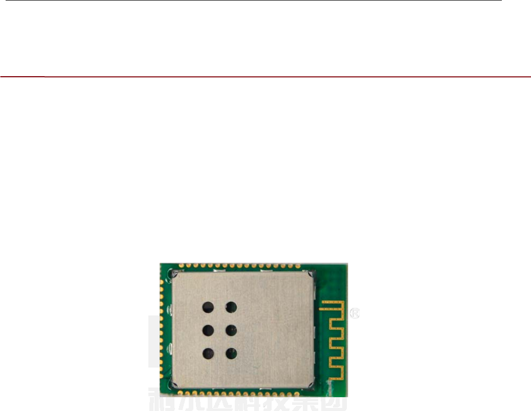
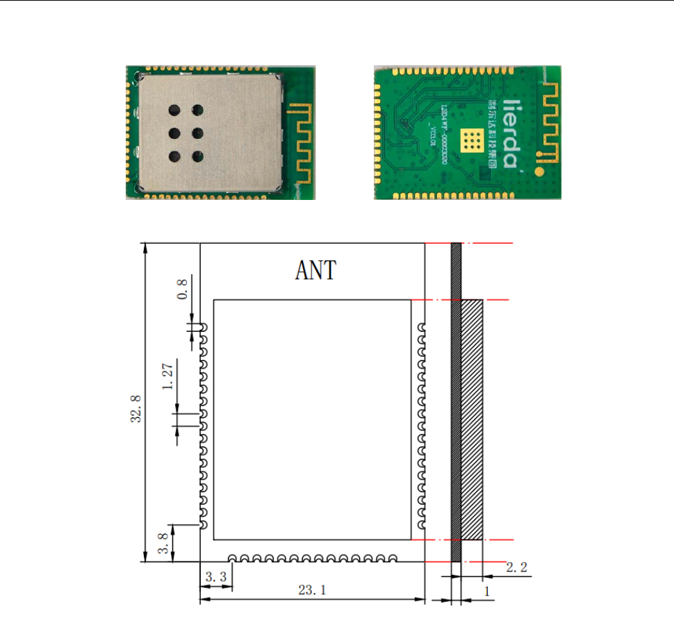
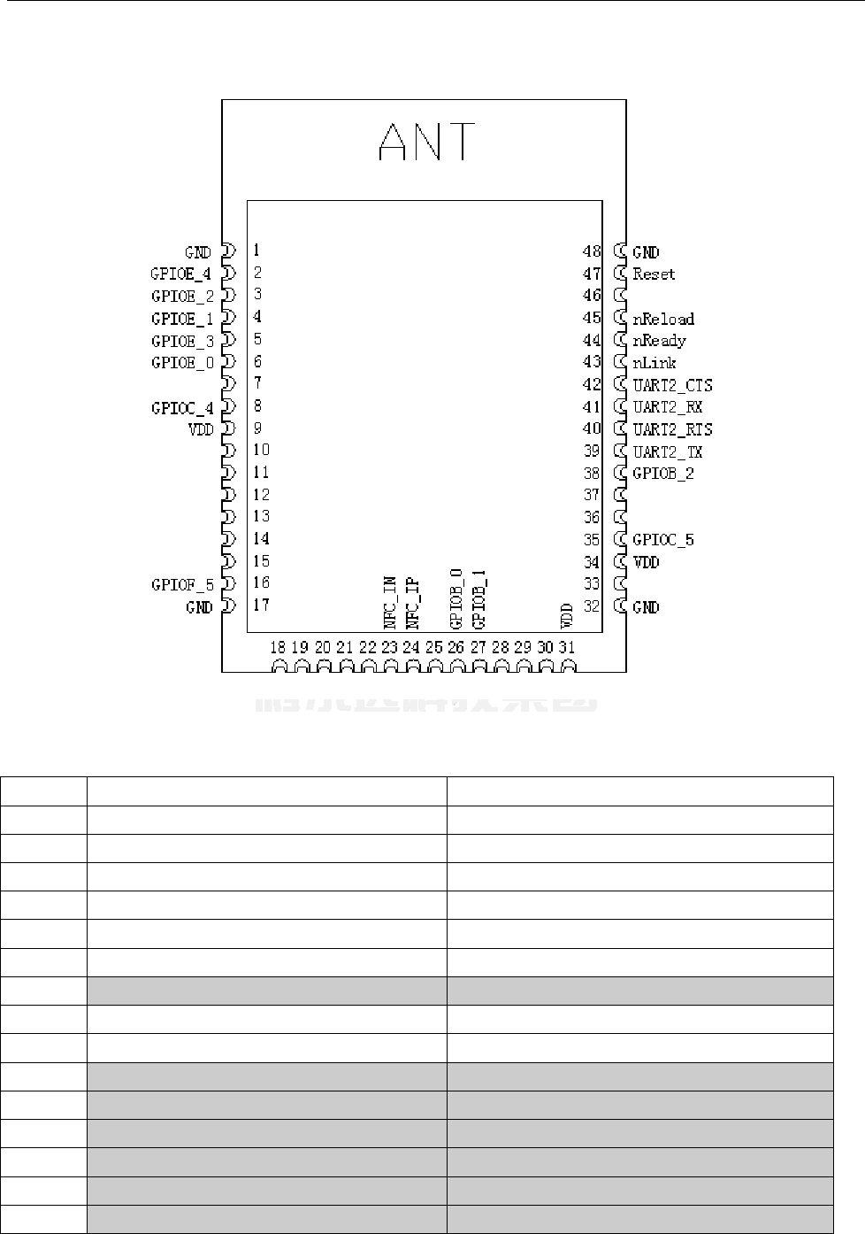
32.8mmx23.1mmx3.2mm, using the stamp hole package, built-in board PCB antenna.
1.2Features
Confirm with 802.11b/g/n protocol.
Built-in high performance M3 core MCU, highest frequency 166MHz, high speed data
processing ability.
USART/GPIO/SPI/PWM multiple interface.
QJoine high speed link configuration.
Support STA/AP/STA+AP coexist work mode.
Support WPA/WPA2/WEP encryption.
Support wireless, Web page and OTA remote hardware upgrading.
Support multiple net protocol communication.
Provide abundant AT+ instruction set configuration.
Optional built-in on board PCB antenna and external antenna interface.
Dimension:32.8mmx23.1mmx3.2mm, Stamp hole paste.
3.3V single power supply.
CE/FCC.
RoHS.

4
2. Parameters
Parameters
Wireless
Parameters
Standard 802.11 b/g/n
Frequency 2.412GHz-2.462GHz
Emitting power
802.11b:+17.0±0.5dBm(@11Mbps)
802.11g:+15.5±0.5dBm(@54Mbps)
802.11n:+15.5±0.5dBm(@HT20,MCS7)
Receiving
Sensitivity
802.11b: -83 dBm (@1Mbps ,CCK)
802.11g: -74dBm (@54Mbps, OFDM)
802.11n: -61dBm (@HT20, MCS7)
Type of
Modulation
802.11g/n OFDM(BPSK,QPSK,16QAM,64QAM)
802.11bCCK11Mbps,5.5Mbps,QPSK2Mbps,BPS
K 1Mbps
Antenna Built-in:On board PCB antenna 2dBi
Hardware
Parameters
Working Voltage 3.3V(3.0V~3.6V)
Working Current Quiescent Current:~20mA
Emitting peak Current:~200mA
Working
Temperature -20 ~ 85℃℃
Hardware
Interface USART/GPIO/SPI/PWM
Dimension 32.8mmx23.1mmx3.2mm
Software
parameters
Wireless network
type STA/AP/STA+AP
Security
Mechanism WEP/WPA-PSK/WPA2-PSK
Encryption WEP/AES/TKIP
Hardware
upgrading
Local wireless upgrading/ Web page
upgrading/ Remote upgrading
Network Protocol IPv4, TCP/UDP/FTP/HTTP
User
Configuration
QJoine Configuration,AT+instruction,Web
page
Pic1-1 LSD4WF-2MD05106 Basic Parameters
5
3. Package
Pic 1-2 LSD4WF-2MD05106 Front and back
Unit:mm
Pic 1-3 LSD4WF-2MD05106 module package dimension
6
4. Pindefinition
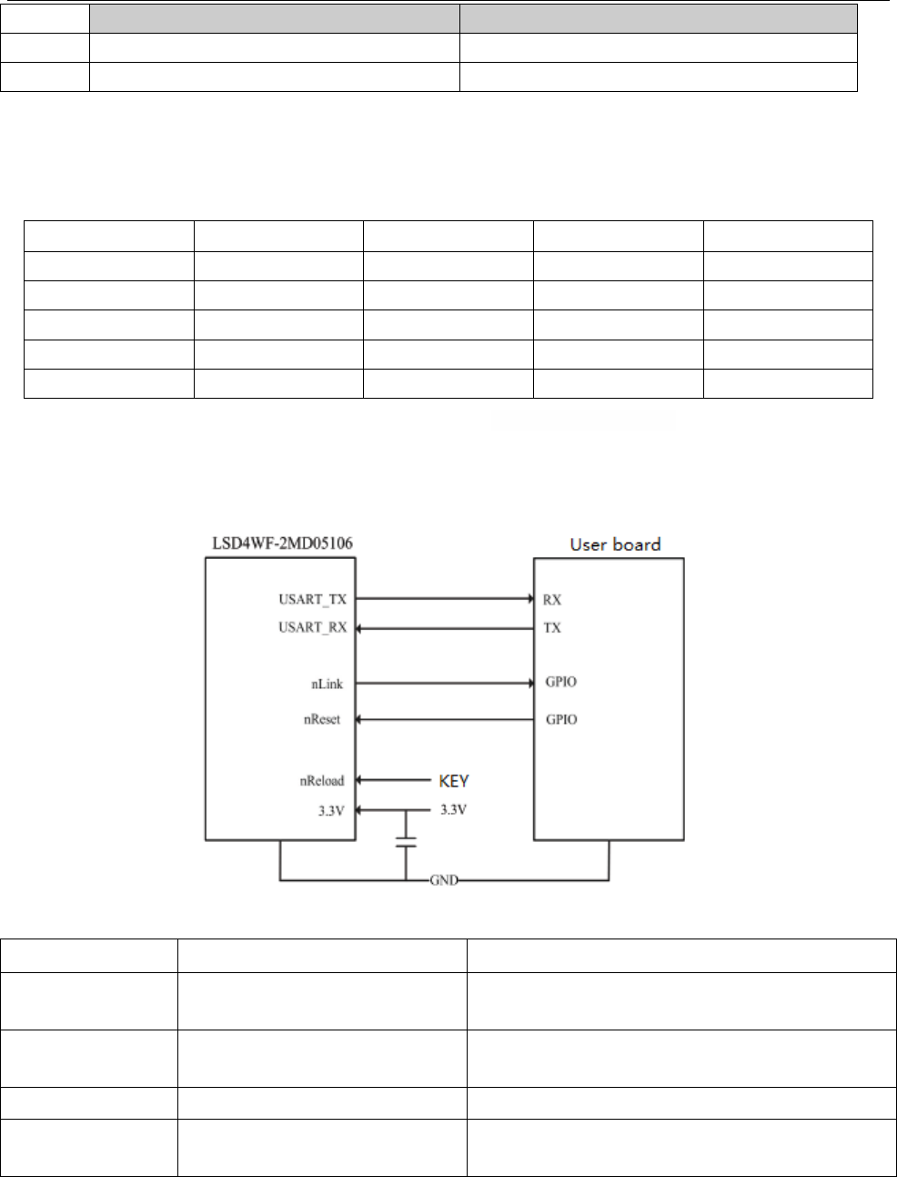
Pic 1-4 LSD4WF-2MD05106 Module pin layout
PINPinDefinitionFunction
1GNDGround pin
2JTAG_CLK/GPIOE_4Program download port
3JTAG_TDO/PWM2/SPI0_MOSI/GPIOE_2 Program download port
4JTAG_TDI/PWM1/SPI0_CLK/GPIOE_1Program download port
5JTAG_TMS/PWM3/SPI0_MISO/GPIOE_3 Program download port
6PWM0/SPI0_CS0/GPIOE_1Multiplex pin
7NCNC
8GPIOC_4GPIO
9VDDVCC(DC_3.3V)
10NCNC
11NCNC
12NCNC
13NCNC
14NCNC
15NCNC

7
16GPIOF_5
EEPROM_SEL
0:Internal NV memory select
1:External EEPROM select
Define:pull-down
17GNDGround pin
18NCNC
19NCNC
20NCNC
21NCNC
22NCNC
23NFC_INNFC+
24NFC_IPNFC‐
25NCNC
26GPIOB_0
BOOT_SCENARIO
0:booting from internal memory
1:booting flash
Define: pull-down
27 GPIOB_1GPIO
28NCNC
29NCNC
30NCNC
31VDDVCC(DC_3.3V)
32GNDGround pin
33NCNC
34VDDVCC(DC_3.3V)
35GPIOC_5GPIO
36NCNC
37NCNC
38GPIOB_2
NORMAL_MODE_SEL
0:Normal operation mode
1:Enter into debug mode
Define:pull-down
39UART2_TX/GPIOA_4UART2/IOPIN
40 UART2_RTS/GPIOA_2UART2/IOPIN
41UART2_RX/GPIOA_0UART2/IOPIN
42 UART2_CTS/GPIOA_1UART2/IOPIN
43
GPIOA_5(nLink)
WIFILED
“0”WIFInoConnection
“1”WIFIConnection
44GPIOA_3(nReady)Modulestartupinstructions
“0:start
“1”nostart
45 GPIOB_3(nReload)Restorefactorysettings
8
46NCNC
47ResetReset pin
48GNDGround pin
Table 1-1 LSD4WF-2MD05106 Module pin definition
5. Behaviorofelectricity
Parameters Minimum Typical value Maximum Unit
Working voltage 3.0 3.3 3.6 V
Standby current 15 mA
Static current 26 mA
TX current 160 mA
RX current 65 mA
Table1-2 LSD4WF-2MD05106 behavior of electricity
6. Typicalapplication
Pic1-5 LSD4WF-2MD05106 Typical circuit connection
Pin State Remark
nlink Output (connected to LED) Check the network state of module or indication
for batch upgrade or configuration
nReload Input, valid in low level Connect button to chip pin for factory setting
restoring
nReset Input, valid in low level Reset pin
USART_TX/USAR
T_RX
Serial port transceiver port Serial port transceiver port
Table 1-3 Connection introduction of cardinal pin
9
7. Referencedesign
PCB onboard antenna is built in LSD4WF-2MD05106 module, users should using onboard antenna
design need to be cautious that:
1, No components or GND on antenna area of user board
2, Keep antenna away from metal, stay over 10mm away from surrounding higher components.
3, Antenna can’t be covered by metal case and it should be over 10mm away from plastic casing.
During specific design, users can consult the Lierda technical engineer to assist in the place of the
module and related Layout.
8. Developingtool
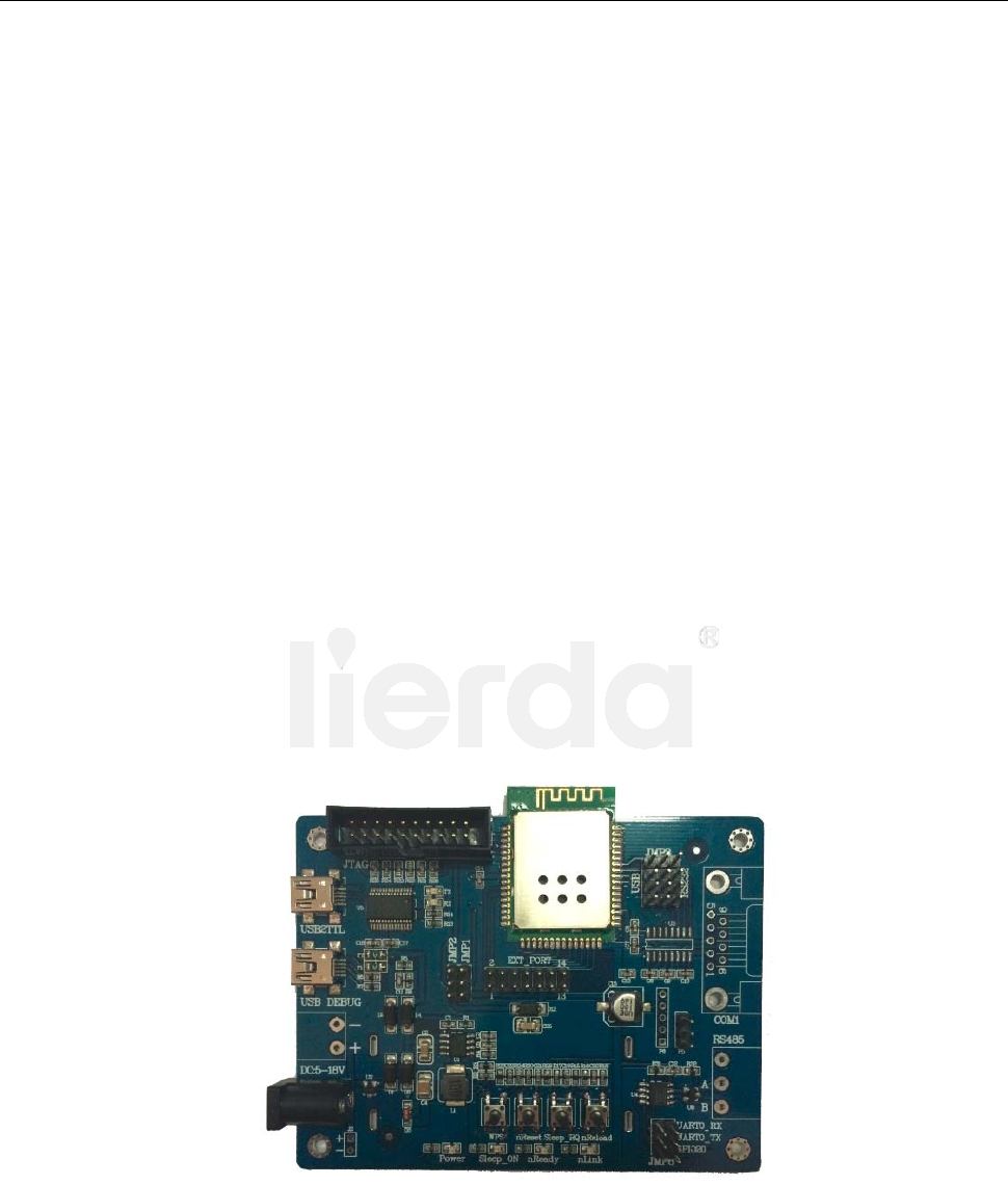
Lierda would provide a complete set of LSD4WF-2MD05106 development kit for customers to get
familiar with the application and development of the module. Users can configure and debug the
parameters of the LSD4WF-2MD05106 module through the USB interface and the function test. This
development board can directly get power from the USB interface, it also support lithium battery and DC
5~18V DC current supply, convenient for the user.
Pic 1-6 Developing board (front)
10
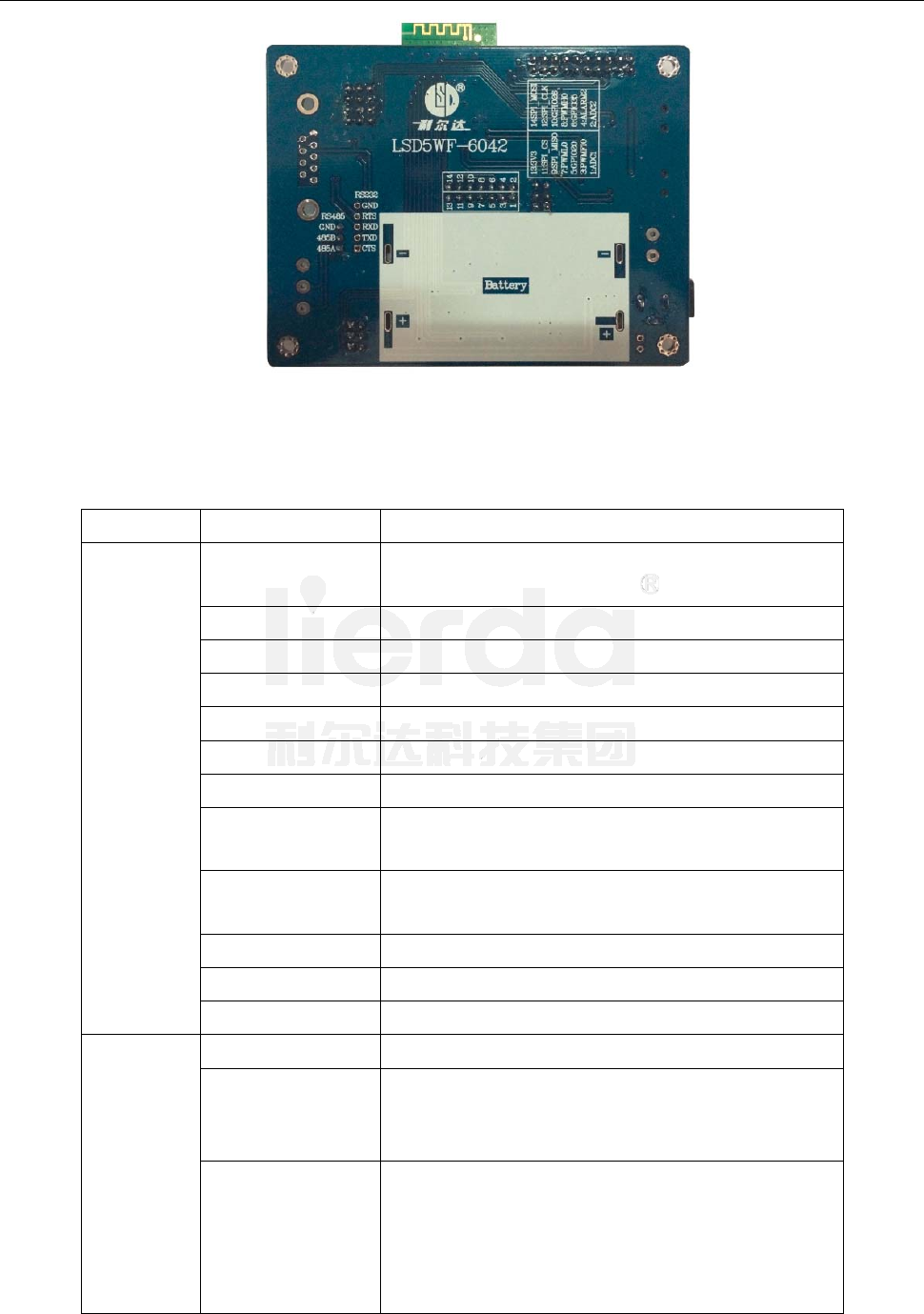
Pic 1-7 Developing board (back)
External interface introduction, table: 1-4
Function Item Description
External
interface
USB2TTL UART to USB debugging port, can be used for
power supply
USB DEBUG USB2.0 debugging interface(reserved)
DC5-18V 5~18V DC input
COM1 RS232 interface
RS485 RS485 interface
JMP1 Preserve
JMP2 Preserve
JMP3 4Pin USB and RS232 debugging choosing port, left
choose USB
JPM6 3Pin RS485 and
RS232 debugging choosing port,
no wire jumper choose RS232
EXT_PORT LSD4WF-2MD05106 GPIO interface expand
JTAG JTAG data debugging interface
Battery Lithium battery supply interface
LED
indication
light
Power 3.3V power indication
Sleep_ON
Module standby indication
On:Module is in standby mode
Off:Module is working
nReady
Module start or updating ready indication
On:Module started up
Off:Module not started
Blink:Remote updating, blink frequency in
proportion to download speed
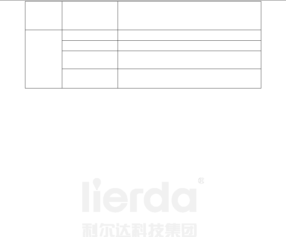
11
nLink
Module connection indication
On:Wi-Fi connected;
Off:Wi-Fi unconnected;
Button
WPS Function reserve
nReset Reset
Sleep_RQ Function reserve
nReload Press button for over 4 seconds to restore to factory
settings.
Table 1-4 External interface introduction of LSD4WF-2MD05106developing board