Linx Technologies 900MCA Hummingbird MCA User Manual User Guide PRO
Linx Technologies Hummingbird MCA User Guide PRO
Contents
User Guide - PRO

HumPROTM Series
RF Transceiver Module
Data Guide

Table of Contents
1 Description
1 Features
2 Ordering Information
2 Absolute Maximum Ratings
3 Electrical Specications
5 Typical Performance Graphs
10 Pin Assignments
10 Pin Descriptions
12 Pre-Certied Module Pin Assignments
13 Module Dimensions
14 Theory of Operation
15 Module Description
16 Overview
18 Addressing Modes
20 Automatic Addressing
20 Address Register Use
21 Acknowledgements and Assured Delivery
22 Frequency Hopping Spread Spectrum
23 Compatibility with the 250 Series
23 Networking
24 Transmitting Packets
25 Receiving Packets
29 Using the Buffer Empty (BE) Line
30 Exception Engine
32 Carrier Sense Multiple Access (CSMA)
33 Using the Command Response (CRESP) Line
34 Using the CMD Line
34 External Amplier Control
35 AES Encryption
Warning: Some customers may want Linx radio frequency (“RF”)
products to control machinery or devices remotely, including machinery
or devices that can cause death, bodily injuries, and/or property
damage if improperly or inadvertently triggered, particularly in industrial
settings or other applications implicating life-safety concerns (“Life and
Property Safety Situations”).
NO OEM LINX REMOTE CONTROL OR FUNCTION MODULE
SHOULD EVER BE USED IN LIFE AND PROPERTY SAFETY
SITUATIONS. No OEM Linx Remote Control or Function Module
should be modified for Life and Property Safety Situations. Such
modification cannot provide sufficient safety and will void the product’s
regulatory certification and warranty.
Customers may use our (non-Function) Modules, Antenna and
Connectors as part of other systems in Life Safety Situations, but
only with necessary and industry appropriate redundancies and
in compliance with applicable safety standards, including without
limitation, ANSI and NFPA standards. It is solely the responsibility of any
Linx customer who uses one or more of these products to incorporate
appropriate redundancies and safety standards for the Life and
Property Safety Situation application.
Do not use this or any Linx product to trigger an action directly
from the data line or RSSI lines without a protocol or encoder/
decoder to validate the data. Without validation, any signal from
another unrelated transmitter in the environment received by the module
could inadvertently trigger the action.
All RF products are susceptible to RF interference that can prevent
communication. RF products without frequency agility or hopping
implemented are more subject to interference. This module does have
a frequency hopping protocol built in, but the developer should still be
aware of the risk of interference.
Do not use any Linx product over the limits in this data guide.
Excessive voltage or extended operation at the maximum voltage could
cause product failure. Exceeding the reflow temperature profile could
cause product failure which is not immediately evident.
Do not make any physical or electrical modifications to any Linx
product. This will void the warranty and regulatory and UL certifications
and may cause product failure which is not immediately evident.
!

– –
1
Description
The HumPROTM Series is a frequency hopping
spread spectrum (FHSS) transceiver designed
for the reliable transfer of digital data. It has a
very fast lock time so that it can quickly wake
up, send data and go back to sleep, saving
power in battery-powered applications. The
module is available in the 915MHz frequency
band.
The module has several features that increase the data transfer reliability. It
ensures that no other modules are transmitting before it begins transmitting
data. Automatic acknowledgements ensure that the remote side received
valid data. Multiple hopping patterns enable several systems to operate
in proximity without interference. A standard UART interface is used for
module configuration and data transfer. A few simple serial commands are
all that are needed for configuration.
All modules have a unique 32-bit serial number that can be used as an
address. Source and destination addressing support point-to-point and
broadcast links. Address masking by the receiving module allows for
creating subnets. Other network topologies can also be implemented.
Housed in a tiny compact reflow-compatible SMD package, the transceiver
requires no external RF components except an antenna, which greatly
simplifies integration and lowers assembly costs. Versions are available that
have obtained FCC and Industry Canada modular certification.
Features
• FHSS Algorithm
• Fast Lock (<30ms at 115kbps)
• Low power modes
• FCC and IC Pre-certified version
• Simple UART interface
• No external RF components
required
• No production tuning required
• Tiny PLCC-32 footprint
HumPROTM Series
RF Transceiver Module
Data Guide
Figure 1: Package Dimensions
Revised 4/8/2015
0.45"
(11.43)
0.55"
(13.97)
0.07"
(1.78)
38 Using the MODE_IND Line
39 Using the PB Line
40 Restore Factory Defaults
40 Using the Low Power Features
42 The Command Data Interface
43 Reading from Registers
44 Writing to Registers
45 Command Length Optimization
45 Example Code for Encoding Read/Write Commands
48 The Command Data Interface Command Set
95 Typical Applications
96 Usage Guidelines for FCC Compliance
96 Additional Testing Requirements
97 Information to the user
98 Product Labeling
98 FCC RF Exposure Statement
98 Antenna Selection
100 Castellation Version Reference Design
102 Power Supply Requirements
102 Antenna Considerations
103 Interference Considerations
104 Pad Layout
105 Microstrip Details
106 Board Layout Guidelines
107 Helpful Application Notes from Linx
108 Production Guidelines
108 Hand Assembly
108 Automated Assembly
110 General Antenna Rules
112 Common Antenna Styles
114 Regulatory Considerations
– – – –
2 3
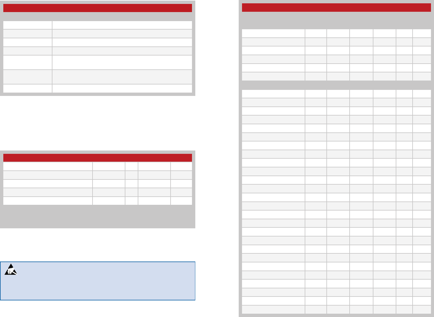
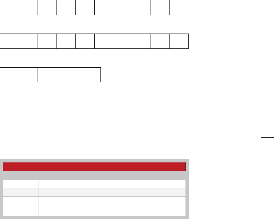
HumPROTM Series Transceiver Specifications
Parameter Symbol Min. Typ. Max. Units Notes
Power Supply
Operating Voltage VCC 2.0 3.6 VDC
TX Supply Current lCCTX
900MHz at +10dBm 40.5 41.5 mA 1,2
900MHz at 0dBm 22 24 mA 1,2
RX Supply Current lCCRX 23.5 24.5 mA 1,2,3
Power-Down Current lPDN 0.7 6 µA 1,2
RF Section
Operating Frequency Band FCMHz
HUM-900-PRO-xxx 902 928 MHz
Number of hop channels
@ 19.2kbps RF Rate 50/64
@ 152.34kbps RF Rate 26/32
Channel spacing
@ 19.2kbps RF Rate 375.9 kHz
@ 152.34kbps RF Rate 751.81 kHz
20 dB OBW
@ 19.2kbps RF Rate 64 kHz
@ 152.34kbps RF Rate 315 kHz
Receiver BW
@ 19.2kbps RF Rate 102 kHz
@ 152.34kbps RF Rate 232 kHz
FSK deviation
@ 19.2kbps RF Rate ± 19.2 kHz
@ 152.34kbps RF Rate ± 51 kHz
Scan time / channel (avg)
@ 19.2kbps RF Rate 1.2 ms
@ 152.34kbps RF Rate 0.335 ms
FHSS Lock time
@ 19.2kbps RF Rate 63 ms
@ 152.34kbps RF Rate 26 ms
Modulation 2FSK
Data Encoding 6/7 RLL
Number of Hop Sequences 6
Electrical SpecicationsOrdering Information
Figure 2: Ordering Information
Warning: This product incorporates numerous static-sensitive
components. Always wear an ESD wrist strap and observe proper ESD
handling procedures when working with this device. Failure to observe
this precaution may result in module damage or failure.
Absolute Maximum Ratings
Supply Voltage Vcc −0.3 to +3.9 VDC
Any Input or Output Pin −0.3 to VCC + 0.3 VDC
RF Input 0 dBm
Operating Temperature −40 to +85 ºC
Storage Temperature −40 to +85 ºC
Exceeding any of the limits of this section may lead to permanent damage to the device.
Furthermore, extended operation at these maximum ratings may reduce the life of this
device.
Absolute Maximum Ratings
Figure 3: Absolute Maximum Ratings
Ordering Information
Part Number Description
HUM-900-PRO HumPROTM Series Data Transceiver
HUM-900-PRO-CAS HumPROTM Series Data Transceiver with Castellation Connection
HUM-900-PRO-UFL HumPROTM Series Data Transceiver with u.FL Connector
EVM-900-PRO HumPROTM Series Carrier Board
EVM-900-PRO-CAS HumPROTM Series Carrier Board with Certified module,
Castellation Connection
EVM-900-PRO-UFL HumPROTM Series Carrier Board with Certified module, UFL
Connector
MDEV-900-PRO HumPROTM Series Master Development System
– – – –
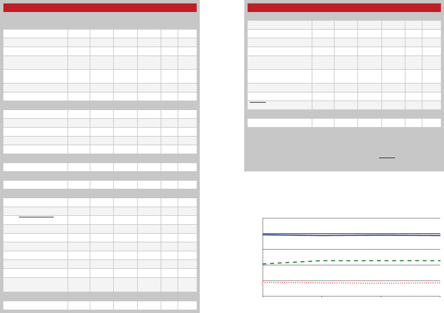
4 5
HumPROTM Series Transceiver Specifications
Parameter Symbol Min. Typ. Max. Units Notes
Input
Logic Low VIL 0.3*VCC VDC
Logic High VIH 0.7*VCC VDC
Output
Logic Low, MODE_IND,
BE VOLM 0.3*VCC VDC 1,9
Logic High, MODE_IND,
BE VOHM 0.7*VCC VDC 1,9
Logic Low VOL 0.3*VCC 1,10
Logic High VOH 0.7*VCC 1,10
CRESP Hold Time 10 Bits 11
Flash (Non-Volatile) Memory Specifications
Flash Write Cycles 22,000 cycles 12
HumPROTM Series Transceiver Specifications
Parameter Symbol Min. Typ. Max. Units Notes
Receiver Section
Spurious Emissions –47 dBm
IF Frequency 304.7 kHz
Receiver Sensitivity 5
HUM-900-PRO-xxx @
min rate –98 –101 dBm 5
HUM-900-PRO-xxx @
max rate –91 –94 dBm 5
RSSI Dynamic Range 85 dB
CSMA RSSI Threshold –70 dBm
Transmitter Section
Output Power PO
HUM-900-PRO-xxx +8.5 +9.5 dBm 6
Harmonic Emissions PH–41 dBc 6
Output Power Range
HUM-900-PRO-xxx PH–5 9 dB 6
Antenna Port
RF Impedance RIN 50 Ω4
Environmental
Operating Temp. Range −40 +85 ºC 4
Timing
Module Turn-On Time
Via VCC 51.7 129.5 ms 4
Via POWER_DOWN 4 ms 4
Via Standby 4 ms 4
Serial Command Response
Volatile R/W 0.4 5 ms 8
NV Update 2.2 31.5 ms 8
Factory Reset 107 ms 8
Channel Dwell Time 400 ms
CMD low to trigger TX with
option TXnCMD tTXnCMD 2 ms
Interface Section
UART Data rate 9,600 115,200 bps
1. Measured at 3.3V VCC
2. Measured at 25ºC
3. Input power < -60dBm
4. Characterized but not tested
5. PER = 5%
6. Into a 50-ohm load
7. No RF interference
8. From end of command to start of
response
9. 60mA source/sink
10. 6mA source/sink
11. End of CMD_DATA_OUT stop bit to
change in CRESP
12. Number of register write operations
Figure 4: Electrical Specifications
Typical Performance Graphs
Figure 5: HumPROTM Series Transceiver Max Output Power vs. Supply Voltage - HUM-900-PRO
8.5
9.0
9.5
10.0
10.5
11.0
2.0 2.5 3.3 3.6
TX Output Power (dBm)
Supply Voltage (V)
85°C
25°C
-40°C
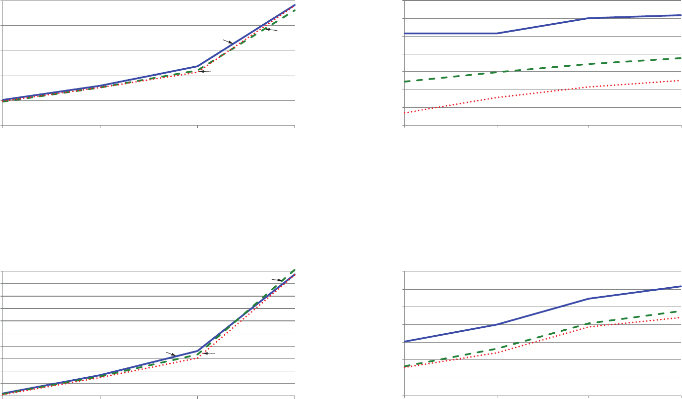
– – – –
6 7
15
20
25
30
35
40
-5
059
Supply Current (mA)
TX Output Power (dBm)
85°C
25°C
-40°C
Figure 6: HumPROTM Series Transceiver Average Current vs. Transmitter Output Power at 2.5V - HUM-900-PRO
20
22
24
26
28
30
32
34
36
38
40
-5
059
Supply Current (mA)
TX Output Power (dBm)
85°C
25°C
-40°C
Figure 7: HumPROTM Series Transceiver Average TX Current vs. Transmitter Output Power at 3.3V -HUM-900-PRO
36.50
37.00
37.50
38.00
38.50
39.00
39.50
40.00
2V 2.5V 3.3V
3.6V
Supply Current (mA)
Supply Voltage (V)
85°C
25°C
-40°C
Figure 9: HumPROTM Series Transceiver TX Current vs. Supply Voltage at Max Power - HUM-900-PRO
22.00
22.20
22.40
22.60
22.80
23.00
23.20
23.40
2V 2.5V 3.3V 3.6V
Supply Current (mA)
Supply Voltage (V)
85°C
25°C
-40°C
Figure 8: HumPROTM Series Transceiver TX Current vs. Supply Voltage at 0dBm - HUM-900-PRO
– – – –
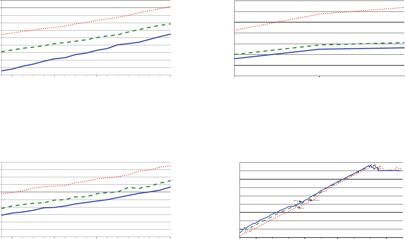
8 9
22.5
22.7
22.9
23.1
23.3
23.5
23.7
23.9
24.1
24.3
24.5
2 2.1 2.2 2.3 2.4 2.5 2.6 2.7 2.8 2.9 3 3.1 3.2 3.3 3.4 3.5 3.6
Supply Current (mA)
Supply Voltage (V)
85°C
25°C
-40°C
Figure 10: HumPROTM Series Transceiver RX Scan Current vs. Supply Voltage, 9.6kbps - HUM-900-PRO
0.00
0.20
0.40
0.60
0.80
1.00
1.20
1.40
2.5 3.3 3.6
Standby Current (µA)
Supply Voltage (V)
-40°C
25°C
85°C
Figure 12: HumPROTM Series Transceiver Standby Current Consumption vs. Supply Voltage - HUM-900-PRO
-105.00
-95.00
-85.00
-75.00
-65.00
-55.00
-45.00
-35.00
-25.00
-15.00
-100.00 -90.00 -80.00 -70.00 -60.00 -50.00 -40.00 -30.00 -20.00 -10.00
0.00
RSSI Reading (dBm)
Input Power (dBm)
-40°C 25°C
85°C
Figure 13: HumPROTM Series Transceiver RSSI Voltage vs. Input Power - HUM-900-PRO
21
21.2
21.4
21.6
21.8
22
22.2
22.4
22.6
22.8
23
2 2.1 2.2 2.3 2.4 2.5 2.6 2.7 2.8 2.9 3 3.1 3.2 3.3 3.4 3.5 3.6
Supply Current (mA)
Supply Voltage (V)
85°C
25°C
-40°C
Figure 11: HumPROTM Series Transceiver RX Scan Current vs. Supply Voltage, 115.2kbps - HUM-900-PRO
Current consumption while the module is scanning for a transmission. The current is
approximately 0.5mA higher when receiving data at 9.6kbps.
Current consumption while the module is scanning for a transmission. The current is
approximately 2mA higher when receiving data at 115.2kbps.
– – – –
10 11
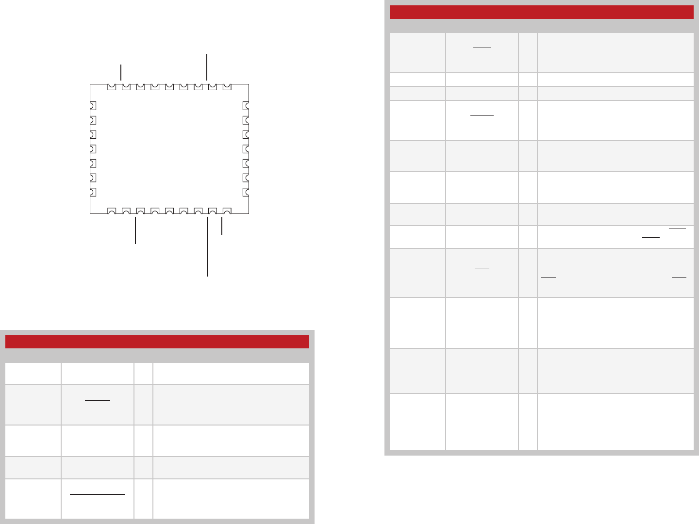
Pin Assignments
30
31
32
1
2
3
4
20
19
18
17
16
15
14
5678 9 10 11 12 13
29 28 27 26 25 24 23 22 21
ANT
GND
GND
GND
GND
GND
GND
BE
MODE_IND
NC
NC
NC
NC
NC
NC
NC
CRESP
EX
NC
NC
GND
CMD
POWER_DOWN
CTS
PB
CMD_DATA_IN
CMD_DATA_OUT
LNA_EN
PA_EN
GND
VCC
RESET
Figure 14: HumPROTM Series Transceiver Pin Assignments (Top View)
Pin Descriptions
Pin Number Name I/O Description
1, 2, 3, 4, 5,
6, 10, 11, 32 NC — No Electrical Connection. Do not connect
any traces to these lines.
7 CRESP O
Command Response. This line is low when
the data on the CMD_DATA_OUT line is
a response to a command and not data
received over the air.
8 EX O
Exception Output. A mask can be set
to take this line high when an exception
occurs.
9, 14, 15, 16,
17, 18, 20, 25 GND — Ground
12 POWER_DOWN I
Power Down. Pulling this line low places the
module into a low-power state. The module
is not functional in this state. Pull high for
normal operation. Do not leave floating.
Pin Descriptions
Pin Number Name I/O Description
13 CMD I
Command Input. When this line is low,
incoming bytes are command data.
When high, incoming bytes are data to be
transmitted.
19 ANTENNA — 50-ohm RF Antenna Port
21 VCC — Supply Voltage
22 RESET I
This line resets the module when pulled low.
It should be high for normal operation. This
line has an internal 10k resistor to supply, so
leave it unconnected if not used.
23 LNA_EN O
Low Noise Amplifier Enable. This line is
driven high when receiving. It is intended to
activate an optional external LNA.
24 PA_EN O
Power Amplifier Enable. This line is driven
high when transmitting. It is intended to
activate an optional external power amplifier.
26 CMD_DATA_OUT O Command Data Out. Output line for data
and serial commands
27 CMD_DATA_IN I Command Data In. Input line for data (CMD
is high) and serial commands (CMD is low).
28 CTS O
UART Clear To Send, active low. This line
indicates to the host microcontroller when
the module is ready to accept data. When
CTS is high, the module is busy. When CTS
is low, the module is ready for data.
29 PB I
Push Button input. This line can be
connected to Vcc through a normally open
push button. Button sequences can reset
configurations to default and join modules
into a network.
30 MODE_IND O
Mode Indicator. This line indicates module
activity. It can source enough current to drive
a small LED, causing it to flash. The duration
of the flashes indicates the module’s current
state.
31 BE O
Buffer Empty. This line is high when the
UART input buffer is empty, indicating
that all data has been transmitted. If
acknowledgment is active, it also indicates
that the receiving module has acknowledged
the data or a retry exception has occurred.
Figure 15: HumPROTM Series Transceiver Pin Descriptions
Pin Descriptions
– – – –
12 13
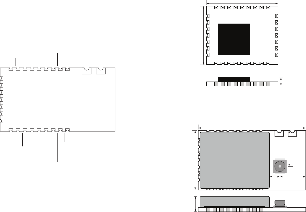
Pre-Certied Module Pin Assignments
The pre-certified version of the module has mostly the same pin
assignments as the standard version. The antenna connection is routed to
either a castellation (-CAS) or a u.FL connector (-UFL), depending on the
part number ordered.
The antenna pad is disconnected on the version with the connector. The
RF is routed as shown in Figure 16 for the version without the connector.
30
31
32
1
2
3
4
19 18
5678 9 10 11 12 13
29 28 27 26 25 24 23 22 21
ANT
GND
BE
MODE_IND
NC
NC
NC
NC
NC
NC
NC
CRESP
EX
NC
NC
GND
CMD
POWER_DOWN
CTS
PB
CMD_DATA_IN
CMD_DATA_OUT
LNA_EN
PA_EN
GND
VCC
RESET
0.45"
(11.43)
0.812"
(20.62)
0.116"
(2.95)
0.271"
(6.88)
0.195"
(4.96)
0.078"
(1.98)
Figure 16: HumPROTM Series Transceiver Pre-certified Version Pin Assignments (Top View)
Module Dimensions
Figure 17: HumPROTM Series Transceiver Dimensions
0.45"
(11.43)
0.55"
(13.97)
0.07"
(1.78)
Figure 18: HumPROTM Series Transceiver Pre-certified Version Dimensions
– – – –
14 15
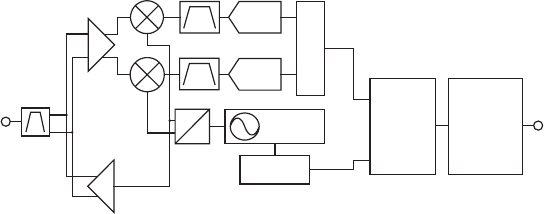
Theory of Operation
The HumPROTM Series transceiver is a low-cost, high-performance
synthesized FSK / MSK transceiver. Figure 19 shows the module’s block
diagram.
The HumPROTM Series transceiver operates in the 902 to 928MHz
frequency band. The transmitter output power is programmable. The
range varies depending on the antenna implementation and the local RF
environment.
The RF carrier is generated directly by a frequency synthesizer that includes
an on-chip VCO. The received RF signal is amplified by a low noise
amplifier (LNA) and down-converted to I/Q quadrature signals. The I/Q
signals are digitized by ADCs.
A low-power onboard communications processor performs the radio
control and management functions including Automatic Gain Control
(AGC), filtering, demodulation and packet synchronization. A control
processor performs the higher level functions and controls the serial and
hardware interfaces.
A crystal oscillator generates the reference frequency for the synthesizer
and clocks for the ADCs and the processor.
PA
LNA
0
90
FREQ
SYNTH
ADC
ADC
DEMODULATOR
MODULATOR
ANTENNA PROCESSORGPIO /
INTERFACE
INTERFACE
Figure 19: HumPROTM Series Transceiver RF Section Block Diagram
Module Description
The HumPROTM Series module is a completely integrated RF transceiver
and processor designed to transmit digital data across a wireless link.
It employs a fast-locking FHSS system for noise immunity and higher
transmitter output power as allowed by government regulations.
When the module does not have data to send it scans all of the channels
for incoming data. If it finds a valid preamble, it pauses and looks for
the start of a packet. When it receives a valid packet with a matching
destination address the module outputs the data through the UART.
The transmitting module accepts packets through its UART until a
configurable number of bytes is reached or a configurable timeout expires
between bytes on the UART. At this point the module transmits the packet.
When the module has data to send it goes to the next channel in its
hopping pattern. It measures the RSSI on that channel to ensure that the
channel is clear. If the RSSI check passes, then it transmits the packets. If
the RSSI fails, then it implements a random wait time and tries again. When
the channel is clear, the module transmits the data.
The module can stay on one channel for up to 400ms. If the module is
ready to start transmitting near the end of the channel time, it transmits the
number of bytes that it can in the remaining time. It then hops to the next
channel in its hopping pattern to transmit the remaining data.
The module supports automatic acknowledgements for assured delivery.
When enabled, the receiving module responds to a valid transmission with
an acknowledgement to let the transmitting module know that it received
the data. If an acknowledgement is not received then the transmitting
module repeats the transmission for a configurable number of retries. If the
retry limit is exceeded without an acknowledgement then the transmitting
module issues an exception error to let the host micro know of the
communication problem.
A standard UART interface is used to configure the module for operation
and for the data input and output. This is suitable for direct connection to
UARTs on many microcontrollers, USB converters and RS-232 converters.
A simple command set is used for configuration and control.
Modules can be pre-configured for fixed point-to-point or broadcast
topologies allowing streaming data (no commands) during operation.

– – – –
16 17
Overview
The HumPROTM Series RF transceiver module offers a number of features
that make it suitable for many data transfer applications. This section
provides a basic overview of the features while following sections dive into
them in more detail.
Addressing
The modules have a very powerful addressing method. Each module is
given a unique 16 or 32 bit address. The receiving modules use an address
mask that determines how it responds to a received transmission.
The addressing and masking allow for the creation of point-to-point,
many-to-one and one-to-many wireless links. This allows the creation of
many network topologies, such as star, tree and mesh. The routing for the
network topology is managed outside the module.
The addressing is the primary configuration when getting started with the
modules. RG-00105, the HumPROTM Addressing Mode Reference Guide
has details about configuring the addressing.
Acknowledgements and Assured Delivery
The modules support assured delivery in the form of acknowledgements
and retries. When the acknowledgements are enabled, the receiving
device sends an acknowledge message to let the sender know that the
transmission was received. If the sender does not get an acknowledgement
it resends the message up to a configurable number of retries. If there is
still no acknowledgement, the module triggers an exception to let the host
processor know of the error.
Command Mode and Data Mode
The module has two main interface modes controlled by the state of the
CMD line. Command mode routes the data coming in on the CMD_DATA_
IN line to the processor for configuring the module. Data mode routes
the data to the transmitter for transmission over-the-air. The CMD line is
normally controlled by an external microcontroller.
Encryption
The module supports AES-128 encryption to provide a secure wireless link.
All of the modules must have encryption enabled and be using the same
key in order for communication to be successful. There are two ways of
entering an encryption key: directly by writing the key to registers through
the Command Data Interface or through a JOIN process.
Streaming Data and Explicit Packets
The module’s default configuration is for streaming data. At some UART
rates the module sends the data at a higher rate over-the-air than it is input
on the UART. This hides the time required for the protocol transactions
and the frequency hopping. The result is that the data appears to stream
through the module with no breaks in the data apparent to the host
processor.
Alternatively, the module can be configured for explicit packet transmission.
This allows the host processor to control when packets are sent and what
data is in each packet
Exceptions and Host Processor Interface
The module has several indicator lines that provide feedback to the host
processor on the module’s operation and current status. This includes an
exception line (EX) that informs the processor when errors occur so that it
can take steps to manage the issue gracefully. The state of the status lines
can also be read through the module’s Command Data Interface to reduce
the number of hardware connections that are required.
Command Data Interface
The module has a Command Data Interface that consists of a set of serial
commands entered through a UART. These are shorter and simpler than AT
commands that are popular with many modules. These commands control
the configuration of the module as well as allow feedback on the operation
and status of the module.
Carrier Sense Multiple Access (CSMA)
The module implements a Carrier Sense Multiple Access method. It listens
to the channel and makes sure that it is clear before it transmits. If the
channel is in use, the module either waits for it to clear or hops to the next
channel depending on its current state. This reduces the overall potential
for interference and improves the robustness of the link.

– – – –
18 19
Addressing Modes
The module has very flexible addressing methods selected with the
ADDMODE register. It can be changed during operation. The transmitting
module addresses packets according to the addressing mode
configuration. The receiving module processes all addressing types
regardless of the ADDMODE configuration. If the received message
matches the addressing criteria, it is output on the UART. Otherwise it is
discarded. The ADDMODE configuration also enables assured delivery.
There are three addressing modes: DSN, User and Extended User. Each
mode offers different communications methods, but all use source and
destination addressing. The source address is for the transmitting unit,
the destination address is the intended receiver. Each mode uses different
registers for the source and destination addresses.
All three addressing modes can be configured to be compatible with the
older 250 Series modules. The default operation has an additional level
of masking on the receiving module that helps prevent interference from
adjacent networks.
The following sections give brief descriptions of the three modes, but a
detailed explanation and examples are given in RG-00105, the HumPROTM
Addressing Mode Reference Guide.
DSN Addressing Mode
Device Serial Number Addressing mode is the simplest mode and
supports point-to-point communications. Each module is programmed at
the factory with a unique 4-byte serial number that cannot be changed.
These bytes are found in the non-volatile read-only MYDSN registers
(MYDSN[3-0]). DSN Addressing mode uses this serial number as an
address. The transmitting unit’s DSN is used as the source address and
the intended receiver’s DSN is written into the destination address registers
(DESTDSN[3-0]). All modules within range hear the transmission, but only
the module with the serial number that matches the destination address
outputs the data on its UART. All others ignore the transmission.
User Addressing Mode
User Addressing Mode is a more flexible method than DSN Addressing
Mode. It uses the customer ID bytes (CUSTID[1-0]) for unencrypted
messages and two of the user destination bytes (UDESTID[1-0]) as a
destination address. The customer ID bytes are programmed at the factory
and cannot be changed. These are determined by the factory for specific
customers to prevent their systems from operating with any other systems.
Contact Linx for more details.
The module’s local address is contained in two of the user source ID
registers (USRCID[1-0]). In this mode, USRCID [1-0] contain the node
address and USRCID [3-2] must be 0 in the receiver.
In normal operation each module has a user ID mask (UMASK[3-0]) that
splits the 32 address bits into up to three fields to provide a network
address and address fields for sub-networks, supporting both individual
addressing and broadcast addressing within the user’s network. A detailed
explanation and examples are given in Reference Guide RG-00105. The
16 bits in the UDESTID[1-0] registers are transmitted. The upper 16 bits of
USRCID[3-2] in the receiver must be 0.
If acknowledgements are enabled, only the module with a user source ID
that exactly matches the transmitted user destination ID responds. The
mask is not used for this determination.
Extended User Addressing Mode
Extended User Addressing mode is the same as User Addressing
mode but uses 32-bit addresses. The two customer ID bytes are still
used (CUSTID[1-0]) but four bytes are used for the user destination
address (UDESTID[3-0]), user source ID (USRCID[3-0]) and user ID mask
(UMASK[3-0]). This provides more addressing capabilities at the expense of
more overhead in the packet.

– – – –
20 21
Acknowledgements and Assured Delivery
When a module transmits with assured delivery enabled, the receiving
module returns an acknowledgement packet. The transmitting module
waits for this acknowledgement for a preset amount of time based on the
data rate. If an acknowledgement is not received, it retransmits the packet.
If the receiver receives more than one of the same packet, it discards
the duplicate packet contents but sends an acknowledgment. This way,
duplicate data is not output by the module.
If the received destination address matches the local address, the
receiving module immediately sends an acknowledgement. This packet
lets the sending module know that the message has been received.
An acknowledgement packet is sent immediately following reception;
CSMA delay is not applied to these packets since permission belongs
to the interacting modules. When the sending module receives the
acknowledgement packet, it marks the current block of data as completed.
If this is the last message in the queue, the sending module takes the BE
line high to indicate that all outgoing data has been sent.
Assured delivery should only be used when addressing a specific module
in a point-to-point link. It should not be used when multiple receivers are
enabled. When address masking is used, only the receiver with an exact
match to the address in the transmitted packet responds. If none of the
enabled receivers has an exact match, then there is no response and the
transmitting module continues to re-transmit the data until the max number
of retries is attempted. This causes the transmitting module to appear slow
or unresponsive. It also impedes valid communications.
Automatic Addressing
The module supports an automatic addressing mode that reads the Source
Address from a valid received packet and uses it to fill the Destination
Address register. This makes sure that a response is sent to the device that
transmitted the original message. This also allows the host microcontroller
to read out the address of the sending unit. The automatic addressing is
enabled for the different addressing modes with register AUTOADDR.
Address Register Use
Figure 20 shows the address registers that are used with each addressing
mode.
Figure 20: HumPROTM Series Transceiver Address Register Use
HumPROTM Series Transceiver Address Registers
COMPAT 0x00 (Relaxed Addressing) 0x02 (Normal Addressing)
ADDMODE
0x04
(DSN)
0x06
(User)
0x07
(Ex User)
0x04
(DSN)
0x06
(User)
0x07
(Ex User)
0x14
(DSN
+ACK)
0x16
(User
+ACK)
0x17
(ExUser
+ACK)
0x14
(DSN
+ACK)
0x16
(User
+ACK)
0x17
(ExUser
+ACK)
UDESTID[3-0] X X
UDESTID[1-0] X X
USRC[3-0] X X X
USRC[1-0] X
UMASK[3-0] X X X
UMASK[1-0] X
DESTDSN[3-0] X X
– – – –
22 23
Frequency Hopping Spread Spectrum
The module uses Frequency Hopping Spread Spectrum to allow operation
at higher power levels per regulations and to reduce interference with other
transmitters. The module is configured for operation in one of 6 different
hopping sequences. Each sequence uses 26 channels for the high RF data
rate or 50 channels for the low RF data rate. Modules must use the same
hopping sequence to communicate. Assigning different hopping sequences
to multiple networks in the same area minimizes the interference.
When the module is awake and not transmitting, it rapidly scans all
channels for a packet preamble. When a module starts transmitting at the
beginning of a new channel, it transmits a packet with a long preamble of
alternating 0 and 1 bits. This long preamble is sufficient to allow receiving
modules to scan through all of the channels in the hopping sequence and
find it. Modules that are scanning detect the preamble and pause on that
channel, waiting for a valid packet.
If a packet is received with a valid CRC (unencrypted) or authentication
(encrypted), the header is examined to determine whether the module
should synchronize to the transmitter. Synchronization requires that the hop
sequence matches and that the message is addressed to the receiver.
When synchronized, the receiver stays on the current channel to either
transmit a packet or to receive an additional packet. Additional packets
transmitted on the same channel within the time slot use short preambles
since the receivers are already listening to the current channel.
At the end of the time slot for the current channel, all modules which locked
to the original transmission switch to the next channel in the hop sequence.
The first transmission on each new channel has a long preamble.
A receiver that has synchronized to a transmitter continues to stay in
synchronism by staying on the received channel until the expiration of the
time slot, then waiting on the next hop channel for the duration of the time
slot. If no further packets are received, the receiver loses lock and reverts
to scanning. This allows the receiver to stay synchronized for a short while
if a packet is not received correctly.
The module supports the option to send the long preamble with every
packet rather than just the first packet on each channel. This can be
beneficial for systems that have modules asleep most of the time. It gives
modules that just woke up the chance to synchronize to any transmitted
packet instead of having to wait for the transmitter to complete its time slot
and jump to the next channel. This can reduce the synchronization time
and power consumption of the sleeping nodes.
Compatibility with the 250 Series
When DSN mode is used with a specific address, the module can
communicate with 250 Series modules at UART data rates of 38,400 to
115,200 bps, non-encrypted. For other addressing modes, the HumPROTM
Series modules can be configured to operate with them. Setting the
COMPAT register to 0x00 enables the compatible operation. This allows
mixed-mode systems and upgrades of legacy products that still maintain
backwards compatibility. Only the higher baud rates are compatible.
The main feature of compatibility operation is that it configures the same
addressing methods used by the 250 Series. These methods are more
susceptible to interference from adjacent networks of 250 Series modules
which use DSN (GUI) broadcast messages. Please see Reference Guide
RG-00105 for more details.
Networking
The HumPROTM Series modules can be used to create many types of
wireless networks. The modules do not provide network routing since the
internal memory size of the module would limit the overall network size. The
HumPROTM can work as the MAC/PHY layers of a network stack and the
memory and processing speed of the external microcontroller can be sized
according to the size of the network that is needed for the application.
This requires more software development, but avoids the cost of adding
extra memory on the module for applications that don’t need it. Linx can
assist with network frameworks and concepts and can create custom
designs on a contract basis. Contact Linx for more details.

– – – –
24 25
Transmitting Packets
In default operation when transmitting, the host microcontroller writes bytes
to the CMD_DATA_IN line while the CMD line is held high at the baud rate
selected by the UARTBAUD register. The incoming bytes are buffered until
one of four conditions triggers the packet to be transmitted:
1. The number of bytes in the buffer exceeds the value in the Byte Count
Trigger (BCTRIG) register.
2. The time since the last received byte exceeds the value in the Data
Timeout (DATATO) register.
3. A SENDP command is written to the CMD register.
4. The CMD line is taken low with option PKOPT: TXnCMD = 1.
5. The number of buffered bytes exceeds what can be sent before the
radio must hop channels.
The first four conditions can be controlled by the host microcontroller. In
the last case, the module transmits what it can in the remaining time then
sends the rest on the next channel. This can cause the data to be divided
up into multiple packets and is not within the control of the host micro.
In cases where all data needs to be sent in the same packet or where the
microcontroller needs greater control over the radio, the HumPROTM offers
explicit control of packet transmission with options in the PKTOPT register.
When the TXPKT option is enabled (PKTOPT register, bit 0 = 1), the data is
held until a SENDP command is written to the CMD register. Alternatively, if
option TXnCMD is enabled (PKTOPT register, bit 1 = 1), then lowering the
CMD line triggers the packet transmission, reducing the number of UART
transactions that are required. The BCTRIG and DATATO conditions are
ignored when the TXPKT option is enabled.
Once triggered, the transmitted packet contains the bytes in the buffer as
of the trigger event, even if more data bytes are received before the packet
can be sent. Multiple outgoing packets can be buffered in this way.
If the full packet cannot be sent in the time remaining on the current
channel, then it is held until the module hops to the next channel.
This option gives the host microcontroller very fine control over when
packets are transmitted and what they contain.
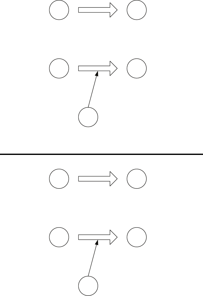
Receiving Packets
In default operation when receiving valid packets, the module outputs all
received bytes as soon as the packet is validated (CRC checks pass) and
if the addressing permits it at the baud rate selected by the UARTBAUD
register. No command or control bytes are output and no action is required
of an external microcontroller. The first byte from a packet directly follows
the last byte of the previously received packet.
In cases where the host microcontroller needs more control over the data
or where dynamic configuration changes could set up race conditions
between incoming data and outgoing commands, the module offers
explicit control over received packets.
When the RXPKT option is enabled (PKTOPT register, bit 2 = 1), received
data is output on the CMD_DATA_OUT line one packet at a time after a
GETPH, GETPD, or GETPHD command is written to the CMD register.
Writing one of these commands begins the received packet transfer cycle.
Two lines are used as flow control and indicators during the transfer cycle.
The CMD line is controlled by the host microcontroller. The module uses
either the CTS line or the CRESP line as a status line, depending on the
state of the RXP_CTS option in the PKOPT register.
When a valid packet is received, the EX_RXWAIT exception flag is set in
the EEXFLAG1 register. If the corresponding bit in the EEXMASK1 register
is set, then the EX line goes high. The host microcontroller can monitor
the EX line or periodically check the EEXFLAG or LSTATUS registers to
determine if data is ready to be read.
The transfer cycle is begun by writing a Get Packet Header (GETPH),
Get Packet Data (GETPD), or Get Packet Header and Data (GETPHD)
command to the CMD register. The module sends the command ACK byte
and sets the selected status line high. Once the status line goes high, the
host microcontroller sets the CMD line high and the module outputs the
received data. The command sent determines whether the bytes sent are
the header, data, or header followed by data.
When all packet bytes have been sent the control line goes low. When
the host microcontroller detects that the line is low, it sets CMD low,
completing the transfer cycle. The cycle is shown in Figure 21.
– – – –
26 27
The Cust ID field is a number that can be assigned to a specific customer.
Only modules with the same customer ID respond to transmissions. By
default, Cust ID is 0x7FFF for packets transmitted with COMPAT = 2 or
0xFFFF for packets transmitted with COMPAT = 0.
The Dest Addr field has the received destination address. This is 2 bytes
long with User Addressing Mode and 4 bytes with DSN and Extended User
Addressing Modes.
The Source Addr Field is the address of the transmitting module. This
is 2 bytes long with User Addressing Mode and 4 bytes with DSN and
Extended User Addressing Modes.
The Data Length byte indicates how many bytes of data are in the packet.
This value is the same in the packet header and the associated data block.
If a GETPH was sent and header data received, the following data can
then be read by repeating the cycle with the GETPD command. If the next
GETPx command is a GETPH or GETPHD, the data associated with the
header read by GETPH is discarded and the header or header plus data of
the following packet is returned.
If there is RF-received data waiting to be sent to the UART and the mask
for EX_RXWAIT is set in the EEXMASK register, EX is raised if it is low.
If there is no packet waiting when a GETPx command is sent, the control
line is still taken high and not reset until after CMD goes high, thereby
performing a zero-byte transfer cycle.
The header and payload structures differ between encrypted packets
and unencrypted packets. The header and data structures for explicit
unencrypted packets are shown in Figure 22.
The Tag field identifies the start of the block and if it is the header
information (0x01) or the packet data (0x02).
The Header Length field identifies the number of header bytes that follow.
The Frame Type field identifies what kind of packet was received. The
values are shown in Figure 23.
The Hop ID field is the hop sequence number, 0 - 5.
The Sequence byte is incremented for each new packet, modulo 255. A
received packet is discarded if the sequence byte matches the previously
received packet to prevent delivering duplicate copies of an automatically
retransmitted packet.
CMD
CMD_DATA_IN
CMD_DATA_OUT
CONTROL
EX
Packet In
Exception for unread packet
Read Packet Command
ACK Packet to UART
Any Command
Any Response
Figure 21: HumPROTM Series Transceiver Received Packet Transfer Cycle
Tag
0x01
Frame
Type
1
Header
Length
1
Hop ID
1
Sequence
1
Dest DSN
4
Source
DSN
4
Data
Length
1
DSN Address Packet Header
Packet Data
Tag
0x02
Data
Data Length Bytes
Data
Length
1
Tag
0x01 1
Header
Length
1
Hop ID
1
Sequence
1
Cust ID
2
Dest Addr
2 or 4
Source
Addr
2 or 4
Source
DSN
4
User Address Packet Header
Data
Length
1
Frame
Type
Figure 22: HumPROTM Series Transceiver Unencrypted Packet Header and Data Structure
Figure 23: HumPROTM Series Transceiver Frame Types
HumPROTM Series Transceiver Frame Types
Frame Type Packet Type
0x04 DSN Addressing Mode
0x06 User Addressing Mode
0x07 Extended User Addressing Mode
+0x10 Acknowledgements Enabled
+0x20 Encrypted Packet
+0x40 Long Preamble Packet
– – – –
28 29
The header and data structures for explicit encrypted packets are shown
in Figure 24. The header and data blocks returned by the module are the
decrypted message contents.
The Tag, Header Length and Frame Type fields are the same as for
unencrypted packets.
The Hop Key field uses the first three low-order bits to indicate the Hop
Sequence number, which is the same as unencrypted packets. The upper
two bits indicate which key is being used. Either the factory-set key that is
used to securely transfer the network key or a network key that has been
written or created by the JOIN process. This is shown in Figure 25.
The Sequence bytes contain a counter that is incremented for each new
transmitted message. The initial value is randomized when the module
is reset. The extended sequence becomes part of an initialization vector
which is used to vary the encrypted contents of identical packets. A
received packet is discarded if the sequence byte matches the previously
received packet to prevent delivering duplicate copies of an automatically
retransmitted packet.
Tag
0x11
Frame
Type
1
Header
Length
1
Hop Key
1
Sequence
6
Dest DSN
4
Source
DSN
4
EBlock
Length
1
Encrypted DSN Address Packet Header
Encrypted Packet Data
Tag
0x12
Data
Data Length Bytes
Data
Length
1
Tag
0x11
Frame
Type
1
Header
Length
1
Hop Key
1
Sequence
6
Dest Addr
2 or 4
Source
Addr
2 or 4
Source
DSN
4
Encrypted User Address Packet Header
EBlock
Length
1
Payload
Type
1
Payload
Type
1
Figure 24: HumPROTM Series Transceiver Encrypted Packet Header and Data Structure
HumPROTM Series HopKey Byte Values
HopKey Bit Value
0 - 3 Hop Sequence Number, 1 to 5
4 - 5 = 0
6 - 7
Encryption key
0 = factory
1 = user network
Figure 25: HumPROTM Series HopKey Byte Values
The Dest DSN, Source DSN, Dest Addr and Source Addr fields are the
source and destination addresses, the same as in unencrypted packets.
The EBlock length filed is the total number of bytes of data in the encrypted
payload block. This length includes the Payload Type byte.
The Payload Type byte indicates what data is contained in the payload.
0x00 indicates that the payload is user data. 0x01 indicates that the
payload is the 16-byte AES key followed by any user data. This is used for
transferring the network encryption key during the JOIN process.
For the Encrypted Packet Data packet, the Data Length byte indicates the
number of bytes of data payload that follow. This value is one less than the
EBlock length in the header. The reason for this is that the Payload Type
byte is included in the encrypted block, but is reported with the header
since it is not user data.
Using the Buffer Empty (BE) Line
The BE line indicates the state of the module’s UART buffer. It is high to
indicate that the UART input buffer is empty, indicating that all data has
been transmitted. When the module receives data on the CMD_DATA_IN
line and the CMD line is high, the BE line is lowered until all data in the
buffer has been processed by the protocol engine. If acknowledgement
is not enabled, the BE line is raised as soon as the module transmits the
outgoing packets. If acknowledgement is enabled, the buffer is not updated
until either the data transmissions are acknowledged by the remote end or
delivery fails after the maximum number of retries. When the BE line returns
high, the EX line may be sampled, or the EXCEPT or EEXFLAG register
polled to determine if an error occurred during transmission.
The state of the BE line can be read in the LSTATUS register, reducing the
number of hardware connections that are needed.

– – – –
30 31
Exception Engine
The HumPROTM is equipped with an internal exception engine to notify the
host microcontroller of an unexpected event. If errors occur during module
operation, an exception is raised. There are two methods of driving the EX
pin when an exception condition exists:
1. From the EXMASK and EXCEPT registers (legacy operation)
2. From the EEXMASKx and EEXFLAGx registers (standard operation)
If EXMASK is non-zero, the first method is used, otherwise the second
method is used.
For legacy operation with the 250 and 25 Series, the EX line is set and
reset by the Exception (EXCEPT) register processing. It is set when
an exception occurs and the exception code ANDed with the current
Exception Mask (EXMASK) register is non-zero. It is reset when the
EXCEPT register is read through a command. No other operations affect
the state of EX. Setting EXMASK non-zero does not change the state of
EX.
If an exception code is already present in the register when an error occurs,
the new exception code overwrites the old value. Exception codes are
organized by type for ease of masking. Figure 26 lists the exception codes
and their meanings.
HumPROTM Series Transceiver Exception Codes
Exception Code Exception Name Description
0x08 EX_BUFOVFL Incoming UART buffer overflowed.
0x09 EX_RFOVFL Outgoing UART buffer overflowed.
0x13 EX_WRITEREGFAILED Attempted write to register failed.
0x20 EX_NORFACK Acknowledgement packet not received
after maximum number of retries.
0x40 EX_BADCRC Bad CRC detected on incoming packet.
0x42 EX_BADHEADER Bad CRC detected in packet header.
0x43 EX_BADSEQID Sequence ID was incorrect in ACK packet.
0x44 EX_BADFRAMETYPE
Attempted transmit with Invalid setting in
reg:NETMODE or invalid packet type in
received packet header
Figure 26: HumPROTM Series Transceiver Exception Codes
The EX line can be asserted to indicate to the host that an error has
occurred. The EXCEPT register must be read to reset the line. Figure 27
lists some example exception masks.
The exception mask has no effect on the exceptions stored in the
exception register. It only controls which exceptions affect the EX line.
The extended exception registers offer more functionality with more
exceptions and a separate bit for each exception. These registers are the
default and should be used with new applications. When an exception sets
an exception code in the EXCEPT register, the corresponding flag in the
EEXFLAG register is also set.
The EX line is set and reset by the Extended Exception Flags (EEXFLAG)
and Extended Exception Mask (EEXMASK) register processing. It is set
whenever the EEXFLAG value ANDed with the EEXMASK value is non-zero.
EX can change on any write to either of these registers that affects the
result of ANDing the registers. Clearing an EEXFLAG register bit or value
can leave EX set if there is another masked condition bit set.
The state of the EX line can also be read in the LSTATUS register, reducing
the number of hardware lines that are required.
HumPROTM Series Transceiver Example Exception Masks
Exception Mask Exception Name
0x08 Allows only EX_BUFOVFL and EX_RFOVFL to trigger the EX line
0x10 Allows only EX_WRITEREGFAILED to trigger the EX line
0x20 Allows only EX_NORFACK to trigger the EX line
0x40 Allows only EX_BADCRC, EX_BADHEADER, EX_BADSEQID and
EX_BADFRAMETYPE exceptions to trigger the EX line
0x60
Allows EX_BADCRC, EX_BADHEADER, EX_BADSEQID, EX_
BADFRAMETYPE and EX_NORFACK exceptions to trigger the EX
line
0xFF Allows all exceptions to trigger the EX line
Figure 27: HumPROTM Series Transceiver Example Exception Masks

– – – –
32 33
Carrier Sense Multiple Access (CSMA)
CSMA is an optional feature. It is a best-effort delivery system that listens
to the channel before transmitting a message. If CSMA is enabled and
the module detects another transmitter on the same channel, it waits until
the active transmitter finishes before sending its payload. This helps to
eliminate RF message corruption and make channel use more efficient.
When a module has data ready to transmit and CSMA is enabled, it listens
on the intended transmit channel for activity. If no signal is detected,
transmission is started.
If a carrier is detected with an RSSI above the CSMA threshold in the
CRSSI register, transmission is inhibited. If a signal below the threshold is
detected that has a compatible preamble or packet structure, transmission
is also inhibited.
If the module is synchronized from a recent packet transfer, it waits for a
random interval, then checks again for activity. If the detected carrier lasts
longer than the time allowed for the current channel, the module hops to
the next channel in the hop sequence and again waits for a clear channel
before transmitting.
If the module is not synchronized, it hops to the next channel and again
checks for interference. When no activity is detected it starts transmitting.
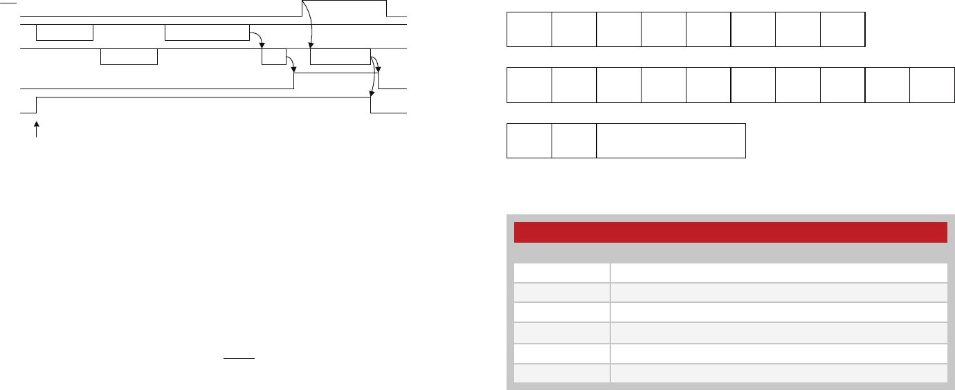
Using the Command Response (CRESP) Line
The CRESP line is normally high, but the module lowers this line when
responding to a UART command. This indicates to an external host
microcontroller that the data on the CMD_DATA_OUT line is a response
to a command and not data received over-the-air. CRESP is held in the
correct state at least one byte time after the last byte for the indicated
source (command response or data, although it normally stays in the same
state until a change is required).
The module normally outputs received RF data immediately following the
command response. The CRESP line does rise before resuming RF data,
but some microcontrollers cannot react quickly enough to this signal and
may not able to separate the command responses from RF data.
When reading or writing the module’s register settings, it is possible for
incoming RF data to intermix with the module’s response to a configuration
command. This can make it difficult to determine if commands were
successfully processed as well as to capture the received RF data. Setting
the CMDHOLD register to 0x01 causes the module to store incoming
RF traffic (up to the RF buffer capacity) while the CMD line is low. When
the CMD line is returned high, the module outputs the buffered data on
the UART. This allows the external host microcontroller to have separate
configuration times and data times instead of potentially having to handle
both at once.
The CRESP line stays low for at least ten bit times after the stop bit of the
last command response. Figure 28 shows the timing.
CMD_DATA_OUT
CRESP
D0 ...D6D710 bit
times
StopStart
Figure 28: HumPROTM Series Transceiver CRESP Line Timing

– – – –
34 35
Using the CMD Line
The CMD line informs the module where incoming UART data should be
routed. When the line is high, all incoming UART data is treated as payload
data and is routed to the transmitter to be sent over the air. If the CMD line
is low, the incoming UART data is treated as command bytes and is routed
to the controller for processing.
Since the module’s controller looks at UART data one byte at a time, the
CMD line must be held low for the entire duration of the command plus
time for ten bits as margin for processing. Leaving the line low for additional
time (for example, until the ACK byte is received by the application) does
not adversely affect the module. If RF packets are received while the CMD
line is active, they are still processed and output on the module’s UART
(assuming CMDHOLD=0 and PKOPT:RXPKT=0). Figure 29 shows this
timing.
Commands can be entered sequentially without having to raise the CMD
line after each one. The CMD line just needs to be raised to be able to
enter data for transmission.
If the CMDHOLD register is 0x01 then any received data is held until the
CMD line is raised. This prevents received data from being intermingled
with command responses.
External Amplier Control
The HumPROTM Series transceiver has two output lines that are designed
to control external amplifiers. The PA_EN line goes high when the module
activates the transmitter. This can be used to activate an external power
amplifier to boost the signal strength of the transmitter. The LNA_EN line
goes high when the module activates the receiver. This can be used to
activate an external low noise amplifier to boost the receiver sensitivity.
These external amplifiers can significantly increase the range of the system
at the expense of higher current consumption and system cost.
The states of the PA_EN and LNA_EN lines can be read in the LSTATUS
register. This offers a quick way to determine the current state of the radio.
CMD_DATA_IN
CMD
D0 ... D6 D7
≥10 bit
times
StopStart
Figure 29: HumPROTM Series Transceiver CMD Line Timing
AES Encryption
HumPROTM Series modules with firmware version 2.0 and above offer AES
encryption. Encryption algorithms are complex mathematical calculations
that use a large number called a key to scramble data before transmission.
This is done so that unauthorized persons who may intercept the signal
cannot access the data. To decrypt the data, the receiver must use the
same key that was used to encrypt it. It performs the same calculations as
the transmitter and if the key is the same, the data is recovered.
The HumPROTM Series module has the option to use AES encryption,
arguably the most common encryption algorithm on the market. This is
implemented in a secure mode of operation to ensure the secrecy of the
transmitted data. It uses a 128-bit key to encrypt the transmitted data. The
source and destination addresses are sent in the clear.
Encryption is disabled by default. There are two ways to enable encryption
and set the key: sending serial commands and using the JOIN process.
Writing an encryption key to the module with the CDI
The module has no network key when shipped from the factory. An
encryption key can be written to the module using the CDI. The CMD
register is used to write or clear a key. The key cannot be read.
The same key must be written to all modules that are to be used together.
If they do not have the same key then they will not communicate in
encrypted mode.
The JOIN Process
The JOIN process is a method of generating an encryption key and
distributing the key and addresses to associated modules through a series
of button presses. This makes it very simple to establish an encrypted
network in the field or add new nodes to an existing network without any
additional equipment. It is also possible to trigger the JOIN process through
commands on the Command Data Interface.
The JOIN process configures a star network with the central unit as system
master. Other units are added to the network one at a time.
The hardware required is a pushbutton that is connected to the PB
line. This takes the line to VCC when it is pressed and ground when it
is released. An LED connected to the MODE_IND line provides visual
indication of the module’s state.
– – – –
36 37
A module is set as a master by pressing and holding the button for 30
seconds to start the Generate Key function. While the button is held, the
MODE_IND line is on. After 30s, the MODE_IND line repeats a double blink,
indicating that the function has begun. When the button is released the key
and address generation is complete and the module is now a master unit.
When Generate Key is performed, the unit is set as the system master
and ADDMODE is set to Extended User Address with encryption (0x27).
It generates a random 128-bit AES encryption key based on ambient RF
noise and scrambled through an encryption operation. If UMASK is the
default value (0xFFFFFFFF), then it is set to 0x000000FF, supporting up to
255 nodes. A random 32-bit address is generated. By default, the lower
8 bits are 0. The address of the master unit is the network base address.
Other nodes are assigned sequential addresses, starting with network
base address +1. Finally, UDESTID is set to the bitwise OR of USRCID and
UMASK, which is the network broadcast address.
Setting a module to be a slave is accomplished by joining it with a master
unit. This is done by pressing and releasing the PB button on both units.
The modules automatically search for each other using a special protocol.
When they find each other, the master sends the slave the encryption key,
UMASK value and its network address. The UDESTID is set to the address
of the master. The values are encrypted using a special key that is defined
at the factory. Once the JOIN process is complete, the MODE_IND blinks
on both units and they now operate together. This is shown in Figure 30 A.
If UMASK is pre-set when Generate Key is initiated, then the JOIN process
uses that mask and sets the address accordingly. This can allow more
nodes in the network. This is shown in Figure 30 B. Likewise, the network
key can be written to the module and the JOIN process used to create an
address and associate new modules. Or the master can be completely
configured through the CDI and the JOIN process used to associate nodes
in the field. This gives the system designer many options for configuration.
The JOIN process protocol detects if there are multiple masters or slaves in
the area attempting to join and fails the process automatically. This ensures
that the correct modules are joined.
The SECOPT register is used to configure options related to the JOIN
process. This allows the OEM to set desired values at the factory and allow
final network configuration in the field. This includes disabling the ability to
change the address, change the key and share the key.
D
UMASK = FF FF FF FF
USRCID = FF FF FF FF
UDESTID = FF FF FF FF
No Key
M
UMASK = 00 00 00 FF
USRCID = 76 54 32 00
UDESTID = 76 54 32 FF
Network Key
Generate Key
D
UMASK = FF FF FF FF
USRCID = FF FF FF FF
UDESTID = FF FF FF FF
No Key
S
UMASK = 00 00 00 FF
USRCID = 76 54 32 01
UDESTID = 76 54 32 00
Network Key
JOIN
M
UMASK = 00 00 00 FF
USRCID = 76 54 32 00
UDESTID = 76 54 32 FF
Network Key
P
UMASK = 00 00 0F FF
USRCID = FF FF FF FF
UDESTID = FF FF FF FF
No Key
M
UMASK = 00 00 0F FF
USRCID = 76 54 30 00
UDESTID = 76 54 3F FF
Network Key
Generate Key
D
UMASK = FF FF FF FF
USRCID = FF FF FF FF
UDESTID = FF FF FF FF
No Key
S
UMASK = 00 00 0F FF
USRCID = 76 54 30 01
UDESTID = 76 54 30 00
Network Key
JOIN
M
UMASK = 00 00 0F FF
USRCID = 76 54 30 00
UDESTID = 76 54 3F FF
Network Key
Key Generation and Network Join from Factory Default
Key Generation and Network Join from Preset Mask
A)
B)
Figure 30: HumPROTM Series JOIN Process
D = Factory Default
M = Network Master
S = Network Slave
P = OEM Preset Unit
– – – –
38 39
Figure 33 shows the MODE_IND displays in a graphical format.
Using the PB Line
The PB Line is used to trigger functions associated with the JOIN process.
This line should be connected to a momentary pushbutton that pulls the
line to VCC when it is pressed and opens the circuit when it is released.
There is no internal pull-down, so a resistor to ground should be used
to pull the line down when the button is not pressed. A value of 10kΩ to
100kΩ works well.
The sequence of presses determines which function is triggered. Figure 32
shows the sequences.
Figure 31: HumPROTM Series MODE_IND Line Timing
Using the MODE_IND Line
The MODE_IND line is designed to be connected to an LED to provide
visual indication of the module’s status and current actions. The pattern of
blinks indicates the particular feedback from the module. Figure 31 shows
the different blink patterns and their meanings.
MODE_IND Line Timing
Display
[on/off time in seconds] Module Status
Join Operation
Two quick blinks Master Join. The master unit is looking for a slave unit to
join with.
One quick blink Slave Join. The slave unit is looking for a master unit to join
with.
Quick blink Key Transfer Active. Key transfer is taking place (master
and slave).
Slow Blink Key Transfer Complete. The module has completed a key
transfer (master and slave).
Temporary On On when the PB line is high
Two quick blinks, one time Join Canceled.
Slow blink, repeat 3 times
Failure. For Share Key or Get Key, there are multiple
units attempting to pair, protocol error, or timeout without
response
Slow blink and two quick
blinks
Long Hold Acknowledgement. The long hold period for
Generate Key or Reset Sequence was recognized (PB is
asserted)
Key Test Results
One quick blink Three
times No Key. There is no network key or network address.
Two quick blinks Three
times
Key Set, slave. The network key and network address are
set on a slave unit.
Three quick blinks Three
times
Key Set, master. The network key and network address are
set on a master unit.
Normal operation
Off No activity
Temporarily on Transmitting or receiving packet
Master Join
Slave Join
Key Transfer Active
Repeats for 30 seconds or until JOIN is complete
Repeats for 30 seconds or until JOIN is complete
Repeats for the duration of the transfer
Key Transfer Complete
JOIN Cancelled
Long Hold
Repeats for as long as the PB line is asserted
after the long hold period has been recognized
Failure
No Key Set
Repeats, three times total
Key Set, Slave
Repeats, three times total
Key Set, Master
Repeats, three times total
OperationMODE_IND Display Comments
Six blinks total
0 0.5 121.5 2.5
Time (seconds)
Figure 33: HumPROTM Series MODE_IND Displays
PB Line Operation
Function Sequence
Join a network 1 short pulse
Cancel a Join Process that is in progress 1 short pulse
Generate a network key and address Hold PB high for 30 seconds
Reset to factory defaults 4 short pulses and hold high for 3 seconds
Test key and address 3 short pulses
A short pulse is a logic high that is between 100 and 2,000ms in duration.
Figure 32: HumPROTM Series PB Line Operation
– – – –
40 41
Restore Factory Defaults
The transceiver is reset to factory default by taking the PB line high briefly
4 times, then holding PB high for more than 3 seconds. Each brief interval
must be high 0.1 to 2 seconds and low 0.1 to 2 seconds. (1 second
nominal high / low cycle). The sequence helps prevent accidental resets.
Once the sequence is recognized, the MODE_IND line blinks in groups
of three until the PB line goes low. After PB goes low, the non-volatile
configurations are set to the factory default values and the module is
restarted. The default UART data rate is 9,600bps.
If the timing on PB does not match the specified limits, the sequence is
ignored. Another attempt can be made after lowering PB for at least 3
seconds.
Using the Low Power Features
The module supports several low-power features to save current in
battery-powered applications. This allows the module to be asleep most of
the time, but be able to quickly wake up, send data and go back to sleep.
Taking the Power Down (POWER_DOWN) line low places the module into
the lowest power state. In this mode, the internal voltage regulator and all
oscillators are turned off. All circuits powered from the voltage regulator
are also off. The module is not functional while in this mode and current
consumption drops to below 6µA. Taking the line high wakes the module.
When the POWER_DOWN line is high, the IDLE register determines sleep
operation.
If IDLE is set to 1 during normal operation, the module sends an ACK byte,
waits for completion of an active transmission, then goes into sleep mode.
Unsent data in the incoming UART data buffer does not inhibit sleep.
During sleep mode, the output lines are in the states in Figure 34.
A rising transition on the POWER_DOWN or CMD_DATA_IN lines wakes
the module. If a negative-going pulse is needed to generate a rising edge,
the pulse width should be greater than 1 µs.
Other lines also wake the module but it immediately goes back to sleep.
Floating inputs should be avoided since they may cause unintended
transitions and cause the module to draw additional current.
If the volatile registers have been corrupted during sleep, a software reset
is performed. This restarts the module as if power were cycled. This can be
caused by power surges or brownout among other things.
After the module wakes up, it sets the IDLE register to 0 (active). If the
WAKEACK register is set to 1, then the module outputs the 0x06 byte on
the CMD_DATA_OUT line. The CRESP line is taken high and the module
then begins normal operation.
Pulsing RESET low causes the module to restart rather than continue from
sleep.
Output Line Sleep States
Output Line Sleep State
EX Unchanged
CRESP Low
LNA_EN Low
PA_EN Low
TXD High
CTS High
MODE_IND Low
BE Unchanged
Figure 34: HumPROTM Series Output Line Sleep States

– – – –
42 43
The Command Data Interface
The HumPROTM Series transceiver has a serial Command Data Interface
(CDI) that is used to configure and control the transceiver through
software commands. This interface consists of a standard UART with a
serial command set. The CMD_DATA_IN and CMD_DATA_OUT lines are
the interface to the module’s UART. The UART is configured for 1 start
bit, 1 stop bit, 8 data bits, no parity and a serial data rate set by register
UARTBAUD (default 9,600bps). The CMD line tells the module if the data
on the UART is for configuration commands (low) or data transmission
(high).
The module has a 256 byte buffer for incoming data. The module starts
transmitting when the buffer reaches a specified limit or when the time
since the last received byte on the UART reaches a specified value. This
allows the designer to optimize the module for fixed length and variable
length data.
If the buffer gets nearly full (about 224 bytes), the module pulls the CTS line
high, indicating that the host should not send any more data. Data sent by
the host while the buffer is full is lost, so the CTS line provides a warning
and should be monitored. When there is outgoing data waiting to be
transmitted or acknowledged the BE line is low, otherwise BE is high.
Configuration settings are stored in two types of memory inside the
module. Volatile memory is quick to access, but it is lost when power is
removed from the module. Non-volatile memory takes longer to access,
but is retained when power is removed. When a configuration parameter
has both a non-volatile and volatile register, the volatile register controls the
operation. The non-volatile register is the default value that is loaded into
the volatile register on power-up.
Configuration settings are read from non-volatile memory on power up
and saved in volatile memory since it is faster to read and write the volatile
memory locations. The volatile and non-volatile registers have different
address locations, but the same read and write commands. The two
locations can be changed independently.
The general serial command format for the module is:
[FF] [Length] [Command]
The Length byte is the number of bytes in the Command field. The
Command field contains the register address that is to be accessed and,
in the case of a write command, the value to be written. Neither Length nor
Command can contain a 0xFF byte.
Byte values of 128 (0x80) or greater can be sent as a two-byte escape
sequence of the format:
0xFE, [value - 0x80]
For example, the value 0x83 becomes 0xFE, 0x03. The Length count
includes the added escape bytes.
A response is returned for all valid commands. The first response byte is
CMD_ACK (0x06) or CMD_NACK (0x15). Additional bytes may follow, as
determined by the specific command.
Reading from Registers
A register read command is constructed by placing an escape character
(0xFE) before the register number. The module responds by sending an
ACK (0x06) followed by the register number and register value. The register
value is sent unmodified, so if the register value is 0x83, 0x83 is returned.
If the register number is invalid, the module responds with a NACK (0x15).
The command and response are shown in Figure 35.
Figure 35: HumPROTM Series Read from Configuration Register Command and Response
HumPROTM Series Read From Configuration Register
Command
Header Size Escape Address
0xFF 0x02 0xFE REG
Response
ACK Address Value
0x06 REG V
Command for an Address greater than 128 (0x80)
Header Size Escape Addr1 Addr2
0xFF 0x03 0xFE 0xFE REG-80
Response
ACK Address Value
0x06 REG V

– – – –
44 45
Writing to Registers
To allow any byte value to be written, values of 128 (0x80) or greater can
be encoded into a two-byte escape sequence of the format 0xFE, [value
- 0x80]. This includes register addresses as well as values to be written to
the registers. The result is that there are four possible packet structures
because of the possible escape sequences. These are shown in Figure 36.
Generally, there are three steps to creating the command.
1. Determine the register address and the value to be written.
2. Encode the address and value as either the number (N) or the encoded
number (0xFE, N-0x80) as appropriate.
3. Add the header (0xFF) and the size.
The module responds with an ACK (0x06). If the ACK is not received, the
command should be resent. The module responds with a NACK (0x15) if a
write is attempted to a read-only or invalid register.
As an example, to write 01 to register 0x83, send
FF 03 FE 03 01
Figure 36: HumPROTM Series Write to Configuration Register Command
HumPROTM Series Write to Configuration Register Command
Command for a Register and Value less than 128 (0x80)
Header Size Address Value
0xFF 0x02 REG V
Command for a Register less than 128 (0x80) and a Value greater than 128 (0x80)
Header Size Address Escape Value
0xFF 0x03 REG 0xFE V-0x80
Command for a Register greater than 128 (0x80) and a Value less than 128 (0x80)
Header Size Addr1 Addr2 Value
0xFF 0x03 0xFE REG-0x80 V
Command for a Register and Value greater than 128 (0x80)
Header Size Addr1 Addr2 Escape Value
0xFF 0x04 0xFE REG-0x80 0xFE V-0x80
Note: The non-volatile memory has a life expectancy of at least 26,000
write operations.
Command Length Optimization
Some commands may be shortened by applying the following rules:
1. Escape sequences are not required for byte values 0x00 to 0xEF
(besides 0xFE and 0xFF, bytes 0xF0 – 0xFD are reserved for future
use).
2. An escape byte inverts bit 7 of the following data byte.
3. The 0xFE as the first byte of the Read Register Command field is an
escape byte.
4. Two consecutive escape bytes cancel unless the following data byte
is 0xf0-0xff.
Examples:
• FF 02 FE 02 (read nv:TXPWR) is equivalent to FF 01 82.
• FF 03 FE FE 53 (read v:PKOPT) is equivalent to FF 01 53.
• FF 03 1A FE 7F (write FF to nv:UMASK0) cannot be shortened.
• FF 03 1A FE 40 (write C0 to nv:UMASK0) is equivalent to FF 02 1A
C0.
These rules are implemented in the sample code file EncodeProCmd.c,
which can be downloaded from the Linx website.

– – – –
46 47
return dx;
}
/* Function: HumProRead
** Description: This function encodes a read command to the specified
** register address.
*/
unsigned char /* number of encoded bytes, 3 to 4 */
HumProRead(
unsigned char *cmd, /* out: encoded read command, length >= 4 */
unsigned char reg /* register number to read, 0..0xff */
) {
unsigned char ra; /* read register byte */
ra = reg ^ 0x80;
return HumProCommand(cmd, &ra, 1);
}
/* Function: HumProWrite
** Description: This function encodes a command to write a single byte to
** a specified register address.
*/
unsigned char /* number of encoded bytes, 4 to 6 */
HumProWrite(
unsigned char *cmd, /* out: encoded read command, length >= 6 */
unsigned char reg, /* register number to write, 0..0xff */
unsigned char val /* value byte, 0..0xff */
) {
unsigned char cs[2];
cs[0] = reg;
cs[1] = val;
return HumProCommand(cmd, &cs, 2);
}
Example Code for Encoding Read/Write Commands
This software example is provided as a courtesy in “as is” condition. Linx
Technologies makes no guarantee, representation, or warranty, whether
express, implied, or statutory, regarding the suitability of the software for
use in a specific application. The company shall not, in any circumstances,
be liable for special, incidental, or consequential damages, for any reason
whatsoever.
File EncodeProCmd.c
/* Sample C code for encoding Hum-xxx-PRO commands
**
** Copyright 2015 Linx Technologies
** 155 Ort Lane
** Merlin, OR, US 97532
** www.linxtechnologies.com
**
** License:
** Permission is granted to use and modify this code, without royalty, for
** any purpose, provided the copyright statement and license are included.
*/
#include “EncodeProCmd.h”
/* Function: HumProCommand
** Description: This function encodes a command byte sequence.
** If len = 1, a read command is generated.
** If len > 1, a write command is generated.
** rcmd[0] = register number
** rcmd[1..(n-1)] = bytes to write
*/
unsigned char /* number of encoded bytes, n+2 to 2*n+2 */
HumProCommand(
unsigned char *ecmd, /* out: encoded command, length >= 2*n + 2 */
const unsigned char *rcmd, /* in: sequence of bytes to encode */
unsigned char n /* number of bytes in rcmd, 1..32 */
) {
unsigned char dx; /* destination index */
unsigned char sx; /* source index */
unsigned char v; /* value to be encoded */
dx = 2;
sx = 0;
while (n--) {
v = rcmd[sx++];
if (v >= 0xf0) {
ecmd[dx++] = 0xfe;
v &= 0x7f;
}
ecmd[dx++] = v;
}
ecmd[0] = 0xff;
ecmd[1] = dx - 2;

– – – –
48 49
DESTDSN0 0x20 0x6B R/W 0xFF Destination Device Serial Number
EXMASK 0x21 0x6C R/W 0x00 Exception Mask to activate EX
CMDHOLD 0x23 0x6E R/W 0x00 Hold RF data when nCMD pin is low
COMPAT 0x25 0x70 R/W 0x02 Compatibility
AUTOADDR 0x26 0x71 R/W 0x00 Automatic Reply Address
MYDSN3 0x34 R Factory programmed Serial Number
MYDSN2 0x35 R Factory programmed Serial Number
MYDSN1 0x36 R Factory programmed Serial Number
MYDSN0 0x37 R Factory programmed Serial Number
CUSTID1 0x39 R 0xFF Factory programmed customer ID
CUSTID0 0x3A R 0xFF Factory programmed customer ID
CRSSI 0x3F R/W 0xBA Carrier Sense minimum RSSI
RELEASE 0x78 R Release number
EXCEPT 0x79 R 0x00 Exception code
PRSSI 0x7B R 0x00 Packet RSSI
ARSSI 0x7C R 0x00 Ambient RSSI
FWVER3 0xC0 R Firmware version, major
FWVER2 0xC1 R Firmware version, minor
FWVER1 0xC2 R Firmware version, increment
FWVER0 0xC3 R Firmware version, suffix
NVCYCLE1 0xC4 R NV Erase Cycles, MS
NVCYCLE0 0xC5 R NV Erase Cycles, LS
LSTATUS 0xC6 R Output line status
CMD 0xC7 W Command register
SECSTAT 0xC9 R Security Status
JOINST 0xCA R 0x00 Join Status
EEXFLAG2 0xCD R/W 0x00 Extended exception flags
EEXFLAG1 0xCE R/W 0x00 Extended exception flags
EEXFLAG0 0xCF R/W 0x00 Extended exception flags
EEXMASK2 0x80 0xD0 R/W 0x00 Extended exception mask
EEXMASK1 0x81 0xD1 R/W 0x00 Extended exception mask
EEXMASK0 0x82 0xD2 R/W 0x00 Extended exception mask
PKTOPT 0x83 0xD3 R/W 0x00 Packet options
SECOPT 0x84 0xD4 R/W 0xFF Security Options
LASTNETAD[3] 0x8C R/W 0x00 Last Network Address Assigned
LASTNETAD[2] 0x8D R/W 0x00 Last Network Address Assigned
LASTNETAD[1] 0x8E R/W 0x00 Last Network Address Assigned
LASTNETAD[0] 0x8F R/W 0x00 Last Network Address Assigned
The Command Data Interface Command Set
The following sections describe the registers.
HumPROTM Series Configuration Registers
Name NV
Addr
Vol
Addr R/W Default
Value Description
CRCERRS 0x40 R/W 0x00 CRC Error Count
HOPTABLE 0x00 0x4B R/W 0x00 Channel Hop Table
TXPWR 0x02 0x4D R/W 0x03 Transmit Power
UARTBAUD 0x03 0x4E R/W 0x01 UART data rate
ADDMODE 0x04 0x4F R/W 0x04 Addressing mode
DATATO 0x05 0x50 R/W 0x10 Data timeout
MAXTXRETRY 0x07 0x52 R/W 0x1A Maximum Transmit Retries
ENCRC 0x08 0x53 R/W 0x01 Enable CRC checking
BCTRIG 0x09 0x54 R/W 0x40 Byte Count trigger
SHOWVER 0x0A R/W 0x01 Show version on startup
ENCSMA 0x0B 0x56 R/W 0x01 Enable CSMA
IDLE 0x0D 0x58 R/W 0x00 Idle Mode
WAKEACK 0x0E 0x59 R/W 0x01 UART Acknowledge on Wake
UDESTID3 0x0F 0x5A R/W 0xFF Destination Address for User Packet
Type, extended
UDESTID2 0x10 0x5B R/W 0xFF Destination Address for User Packet
Type, extended
UDESTID1 0x11 0x5C R/W 0xFF Destination Address for User Packet
Type
UDESTID0 0x12 0x5D R/W 0xFF Destination Address for User Packet
Type
USRCID3 0x13 0x5E R/W 0xFF Source Address for User Packet Type,
extended
USRCID2 0x14 0x5F R/W 0xFF Source Address for User Packet Type,
extended
USRCID1 0x15 0x60 R/W 0xFF Source Address for User Packet Type
USRCID0 0x16 0x61 R/W 0xFF Source Address for User Packet Type
UMASK3 0x17 0x62 R/W 0xFF Address Mask for User Packet Type,
extended
UMASK2 0x18 0x63 R/W 0xFF Address Mask for User Packet Type,
extended
UMASK1 0x19 0x64 R/W 0xFF Address Mask for User Packet Type
UMASK0 0x1A 0x65 R/W 0xFF Address Mask for User Packet Type
DESTDSN3 0x1D 0x68 R/W 0xFF Destination Device Serial Number
DESTDSN2 0x1E 0x69 R/W 0xFF Destination Device Serial Number
DESTDSN1 0x1F 0x6A R/W 0xFF Destination Device Serial Number
Figure 37: HumPROTM Series Configuration Registers

– – – –
50 51
CRCERRS - CRC Error Count
Volatile Address = 0x40
The value in the CRCERRS register is incremented each time a packet with
a valid header is received that fails the CRC check on the payload. This
check applies only to unencrypted packets. Overflows are ignored. Writing
0x00 to this register initializes the count. Figure 38 shows the command
and response.
HOPTABLE - Channel Hop Table
Volatile Address = 0x4B; Non-Volatile Address = 0x00
The module supports 6 different hop sequences with minimal correlation.
The sequence is set by the value in the HOPTABLE register. Changing the
hop sequence changes the band utilization, much the same way that a
channel does for a non-hopping transmitter. The hop table selection must
match between the transmitter and receiver. Valid values are 0-5. Figure 39
shows the command and response.
Figure 40 shows the RF channels used by the HumPROTM Series. When
the baud rate is set to 9,600 or 19,200 bps, the module uses 50 hopping
Figure 38: HumPROTM Series CRC Error Count Command and Response
Figure 39: HumPROTM Series Channel Hop Table Command and Response
HumPROTM Series CRC Error Count
Read Command Read Response
Header Size Escape Address ACK Address Value
0xFF 0x02 0xFE 0x40 0x06 0x40 V
Write Command
Header Size Address Value
0xFF 0x02 0x40 V
HumPROTM Series Channel Hop Table
Read Command Read Response
Header Size Escape Address ACK Address Value
0xFF 0x02 0xFE 0x4B
0x00 0x06 0x4B
0x00 V
Write Command
Header Size Address Value
0xFF 0x02 0x4B
0x00 V
HumPROTM Series RF Channels
Channel Number Frequency (MHz) Channel Number Frequency (MHz)
0 902.971 32 915.000
1 903.347 33 915.376
2 903.723 34 915.752
3 904.099 35 916.128
4 904.475 36 916.504
5 904.851 37 916.880
6 905.227 38 917.255
7 905.602 39 917.631
8 905.978 40 918.007
9 906.354 41 918.383
10 906.730 42 918.759
11 907.106 43 919.135
12 907.482 44 919.511
13 907.858 45 919.887
14 908.234 46 920.263
15 908.610 47 920.639
16 908.986 48 921.014
17 909.361 49 921.390
18 909.737 50 921.766
19 910.113 51 922.142
20 910.489 52 922.518
21 910.865 53 922.894
22 911.241 54 923.270
23 911.617 55 923.646
24 911.993 56 924.022
25 912.369 57 924.398
26 912.745 58 924.773
27 913.120 59 925.149
28 913.496 60 925.525
29 913.872 61 925.901
30 914.248 62 926.277
31 914.624 63 926.653
Figure 40: HumPROTM Series RF Channels
channels. Figure 41 shows the hop sequences referenced by channel
number. When the baud rate is 38,400bps and higher, the module uses 26
hopping channels and only even channels are used. Figure 42 shows the
hop sequences referenced by channel number. The default hop sequence
is 0.

– – – –
52 53
HumPROTM Series Hop Sequences by Channel Number for 38,400bps and Above
0 1 2 3 4 5
32 30 6 56 44 18
2 60 40 22 14 48
4 58 42 20 16 46
10 52 48 14 22 40
20 42 58 4 32 30
42 20 16 46 54 8
22 40 60 2 34 28
46 16 20 42 58 4
28 34 2 60 40 22
58 4 32 30 6 56
54 8 28 34 2 60
44 18 18 44 56 6
24 38 62 0 36 26
48 14 22 40 60 2
34 28 8 54 46 16
6 56 44 18 18 44
14 48 52 10 26 36
30 32 4 58 42 20
62 0 36 26 10 52
60 2 34 28 8 54
56 6 30 32 4 58
50 12 24 38 62 0
38 24 12 50 50 12
12 50 50 12 24 38
26 36 0 62 38 24
52 10 26 36 0 62
Figure 42: HumPROTM Series Hop Sequences for UART rates of 19,200bps and above
HumPROTM Series Hop Sequences by Channel Number for 19,200bps and below
0 1 2 3 4 5
25 30 11 58 52 35
63 60 12 11 10 23
28 59 0 52 54 41
26 14 62 37 62 45
16 16 23 36 21 7
61 32 43 42 33 42
4 4 25 25 44 63
29 47 34 15 51 24
0 26 61 1 61 9
44 43 26 55 36 27
46 1 24 2 34 10
22 25 6 12 2 17
36 36 31 26 57 20
34 15 7 27 50 22
24 57 32 41 12 18
2 10 55 9 29 32
21 48 39 8 6 3
11 21 1 31 8 8
27 8 41 49 46 15
1 17 29 13 48 4
35 37 15 47 11 0
37 45 57 14 39 48
55 44 3 33 4 13
8 13 42 48 45 61
10 33 47 38 22 31
54 0 2 45 56 56
13 46 56 59 18 52
32 62 33 3 43 54
43 34 9 46 60 55
12 7 14 0 31 62
23 24 30 39 47 6
48 22 21 57 0 37
14 58 4 56 20 36
39 42 54 5 37 38
40 50 59 40 59 51
15 12 51 23 35 59
57 20 22 62 7 5
18 39 38 24 15 43
60 27 58 54 25 21
41 2 60 17 16 40
9 35 52 22 23 14
49 5 45 32 42 12
58 28 37 7 24 30
38 49 13 61 32 16
45 29 35 34 28 34
56 18 36 63 26 46
50 38 8 50 13 60
42 3 46 30 3 39
62 52 40 43 5 58
47 40 49 28 49 33
Figure 41: HumPROTM Series Hop Sequences for UART rate of 9,600bps

– – – –
54 55
TXPWR - Transmitter Output Power
Volatile Address = 0x4D; Non-Volatile Address = 0x02
The value in the TXPWR register sets the module’s output power. Figure 43
shows the command and response and Figure 44 available power settings
and typical power outputs for the module. The default setting is 0x03.
HumPROTM Series Transmitter Output Power Mode Register Settings
PWR Typical Output Power (dBm)
0x00 -5
0x01 0
0x02 +5
0x03 +9
Figure 43: HumPROTM Series Transmitter Output Power Mode Command and Response
Figure 44: HumPROTM Series Transmitter Output Power Mode Settings
HumPROTM Series Transmitter Output Power Mode
Read Command Read Response
Header Size Escape Address ACK Address Value
0xFF 0x02 0xFE 0x4D
0x02 0x06 0x4D
0x02 PWR
Write Command
Header Size Address Value
0xFF 0x02 0x4D
0x02 PWR
UARTBAUD - UART Baud Rate
Volatile Address = 0x4E; Non-Volatile Address = 0x03
The value in UARTBAUD sets the data rate of the UART interface.
Changing the non-volatile register changes the data rate on the following
power-up or reset. Changing the volatile register changes the data rate
immediately following the command acknowledgement. Figure 45 shows
the command and response and Figure 46 shows the valid settings.
If the module’s UART baud rate is different than the host processor UART
baud rate then the module will not communicate correctly. If mismatched,
every rate can be tested until the correct one is found or the module can be
reset to factory defaults. The default baud rate is 9,600bps (0x01).
Figure 45: HumPROTM Series UART Baud Rate Command and Response
Figure 46: HumPROTM Series UART Baud Rate Settings
HumPROTM Series UART Baud Rate Register Settings
V Baud Rate (bps) RF Data Rate (bps)
0x01 9,600 19,200
0x02 19,200 19,200
0x03 38,400 153,600
0x04 57,600 153,600
0x05 115,200 153,600
0x06 10,400* 153,600
0x07 31,250* 153,600
* These data rates are not supported by PC serial ports. Selection of these rates may
cause the module to fail to respond to a PC, requiring a reset to factory defaults.
HumPROTM Series UART Baud Rate
Read Command Read Response
Header Size Escape Address ACK Address Value
0xFF 0x02 0xFE 0x4E
0x03 0x06 0x4E
0x03 V
Write Command
Header Size Address Value
0xFF 0x02 0x4E
0x03 V

– – – –
56 57
ADDMODE - Addressing Mode
Volatile Address = 0x4F; Non-Volatile Address = 0x04
The module supports three addressing modes: DSN, User, and Extended
User, which are configured using bits 0 - 2.
If bit 3 is set, the module sends an extended preamble. This allows
modules that have just awakened or have not yet synchronized to find and
temporarily synchronize with the transmitting module. This can be useful
in systems that require the endpoints to spend most of their time sleeping.
Endpoints can awaken, receive a message from the transmitter, and go
back to sleep. This message could contain scheduling information as to
when to wake again for a full bi-directional communications session.
If bit 4 is set, then the receiver is instructed to transmit an
acknowledgement packet for assured delivery signifying to the transmitter
that the message was received.
If bit 5 is set then the module transmits data in encrypted mode.
Figure 47 shows the command and response and Figure 48 shows the
valid settings.
HumPROTM Series Addressing Mode Register Settings
Addressing Mode Meaning
0x04 DSN Addressing Mode
0x06 User Addressing Mode
0x07 Extended User Addressing Mode
+0x00 Send normal preamble
+0x08 Send long preamble
+0x10 Send acknowledgments
+0x20 Encrypt packets
All other addressing modes are reserved and may cause undesired operation.
Figure 47: HumPROTM Series Addressing Mode Command and Response
HumPROTM Series Addressing Mode
Read Command Read Response
Header Size Escape Address ACK Address Value
0xFF 0x02 0xFE 0x4F
0x04 0x06 0x4F
0x04 V
Write Command
Header Size Address Value
0xFF 0x02 0x4F
0x04 V
Figure 48: HumPROTM Series Addressing Mode Register Settings

– – – –
58 59
MAXTXRETRY - Maximum Transmit Retries
Volatile Address = 0x52; Non-Volatile Address = 0x07
The value in the MAXTXRETRY register sets the number of transmission
retries performed if an acknowledgement is not received. If an
acknowledgement is not received after the last retry, exception EX_
NORFACK is raised. Figure 51 shows examples of the command.
The time between retries depends on the current baud rate. Figure 52
shows the time between retries based on baud rate. The elapsed transmit
and acknowledgment time is (retries+1) × (PacketTransmitTime + Timeout).
Figure 51: HumPROTM Series Maximum Transmit Retries Command and Response
HumPROTM Series Acknowledgement Timeout Times
Baud Rate Timeout Time
9,600 50ms
19,200 50ms
38,400 30ms
57,600 30ms
115,200 30ms
Figure 52: HumPROTM Series Acknowledgement Timeout Times
HumPROTM Series Maximum Transmit Retries
Read Command Read Response
Header Size Escape Address ACK Address Value
0xFF 0x02 0xFE 0x52
0x07 0x06 0x52
0x07 V
Write Command
Header Size Address Value
0xFF 0x02 0x52
0x07 V
DATATO - Transmit Wait Timeout
Volatile Address = 0x50; Non-Volatile Address = 0x05
When a byte is received from the UART, the module starts a timer that
counts down every millisecond. The timer is restarted when each byte is
received. The value for the DATATO register is the number of milliseconds
to wait before transmitting the data in the UART receive buffer. The default
setting for this register is 0x10 (~16ms delay).
If the timer reaches zero before the next byte is received from the UART,
the module begins transmitting the data in the buffer. This timeout value
should be greater than one byte time at the current UART baud rate with a
minimum of 0x02. It should not be set any value less than one byte time as
unpredictable results could occur.
If the timeout value is set to 0x00, the transmit wait timeout is deactivated.
In this case, the transceiver waits until a number of bytes equal to the
UART Byte Count Trigger (BCTRIG) have been received by the UART. All
of the bytes are sent once the trigger has been reached. Figure 49 shows
examples of the commands. Figure 50 shows the minimum timeout values
based on baud rate.
Figure 49: HumPROTM Series Transmit Wait Timeout Command and Response
HumPROTM Series Minimum DATATO Values
Baud Rate Minimum DATATO
9,600 3ms
19,200 2ms
38,400 2ms
57,600 2ms
115,200 2ms
Figure 50: HumPROTM Series Transmit Wait Timeout Minimum Values
HumPROTM Series Transmit Wait Timeout
Read Command Read Response
Header Size Escape Address ACK Address Value
0xFF 0x02 0xFE 0x50
0x05 0x06 0x50
0x05 V
Write Command
Header Size Address Value
0xFF 0x02 0x50
0x05 V

– – – –
60 61
ENCRC - CRC Enable
Volatile Address = 0x53; Non-Volatile Address = 0x08
The protocol includes a Cyclic Redundancy Check (CRC) on the received
packets to make sure that there are no errors. Any packets with errors are
discarded and not output on the UART. This feature can be disabled if it
is desired to perform error checking outside the module. Set the ENCRC
register to 0x01 to enable CRC checking, or 0x00 to disable it. The
default CRC mode setting is enabled. Figure 53 shows examples of the
commands and Figure 54 shows the available values.
Although disabling CRC checking allows receiving packets with errors
in the payload, errors in the header can still prevent packets from being
output by the module.
HumPROTM Series CRC Enable Register Settings
V Mode
0x00 CRC Disabled
0x01 CRC Enabled
Figure 53: HumPROTM Series CRC Enable Command and Response
Figure 54: HumPROTM Series CRC Enable Register Settings
HumPROTM Series CRC Enable
Read Command Read Response
Header Size Escape Address ACK Address Value
0xFF 0x02 0xFE 0x53
0x08 0x06 0x53
0x08 V
Write Command
Header Size Address Value
0xFF 0x02 0x53
0x08 V
BCTRIG - UART Byte Count Trigger
Volatile Address = 0x54; Non-Volatile Address = 0x09
The BCTRIG register determines the UART buffer level that triggers
the transmission of a packet. The minimum value is decimal 1 and the
maximum value is 192. The default value for this register is 64, which
provides a good mix of throughput and latency. At the maximum data rate,
a value of 128 optimizes throughput. This register does not guarantee a
particular transmission unit size; rather, it specifies the minimum desired
size. If there is not enough time left in the channel dwell time before the
module must hop to the next channel, for instance, the protocol engine
sends as many characters as it can to fill the current channel dwell time,
and sends the remaining characters on the next channel. Figure 55 shows
examples of the commands.
This trigger can be overridden by enabling the TXPKT option (PKTOPT
register, bit 0).
Figure 55: HumPROTM Series UART Byte Count Trigger Command and Response
HumPROTM Series UART Byte Count Trigger
Read Command Read Response
Header Size Escape Address ACK Address Value
0xFF 0x02 0xFE 0x54
0x09 0x06 0x54
0x09 V
Write Command
Header Size Address Value
0xFF 0x02 0x54
0x09 V

– – – –
62 63
SHOWVER - Show Version
Non-Volatile Address = 0x0A
Setting the SHOWVER register to 0x00 suppresses the start-up message,
including firmware version, which is sent out of the UART when the module
is reset. A value of 0x01 causes the message to be output after reset. By
default, the module start-up message is output. Figure 56 shows examples
of the commands and Figure 57 shows the available values.
Example:
HUM-900-PRO v1.2.3
(C) 2014 Linx Technologies Inc. All rights reserved.
Figure 56: HumPROTM Series Show Version Command and Response
Figure 57: HumPROTM Series Show Version Register Settings
HumPROTM Series Show Version Register Settings
V Meaning
0x00 Startup message is NOT output on reset or power-up.
0x01
Startup message is output on reset or power-up. This is a
blocking operation, and any incoming UART data is lost during the
transmission of this message through the CMD_DATA_OUT line. All
UART commands must be sent after this message has completed.
HumPROTM Series Show Version
Read Command Read Response
Header Size Escape Address ACK Address Value
0xFF 0x02 0xFE 0x0A 0x06 0x0A V
Write Command
Header Size Address Value
0xFF 0x02 0x0A V
ENCSMA - CSMA Enable
Volatile Address = 0x56; Non-Volatile Address = 0x0B
Carrier-Sense Multiple Access (CSMA) is a best-effort transmission protocol
that listens to the channel before transmitting a message. If another device
is already transmitting on the same channel at the same baud rate when
a message is ready to send, the module waits before sending its payload.
This helps to eliminate RF message corruption at the expense of additional
latency. By default, CSMA is enabled. Figure 58 shows examples of the
commands and Figure 59 shows the available values.
See the Carrier Sense Multiple Access section for details.
Figure 58: HumPROTM Series CSMA Enable Command and Response
HumPROTM Series CSMA Enable Register Settings
V Mode
0x00 Disable CSMA
0x01 Enable CSMA
Figure 59: HumPROTM Series CSMA Enable Register Settings
HumPROTM Series CSMA Enable
Read Command Read Response
Header Size Escape Address ACK Address Value
0xFF 0x02 0xFE 0x56
0x0B 0x06 0x56
0x0B V
Write Command
Header Size Address Value
0xFF 0x02 0x56
0x0B V

– – – –
64 65
IDLE - Idle Mode
Volatile Address = 0x58; Non-Volatile Address = 0x0D
The value in the IDLE register sets the operating mode of the transceiver.
If the module remains properly powered, and is awakened from a low
power mode properly, the volatile registers retain their values. If the volatile
registers become corrupted during low power, a software reset is forced
and the module reboots.
Awake is the normal operating setting. This is the only setting in which the
RF circuitry is able to receive and transmit RF messages.
Sleep disables all circuitry on-board the module. This is the lowest-power
setting available for the module.
Please see the Low Power States section for more details. Figure 60 shows
examples of the commands and Figure 61 shows the available values.
Figure 60: HumPROTM Series Idle Mode Command and Response
HumPROTM Series Idle Mode Register Settings
V Mode
0x00 Awake
0x01 Sleep
Figure 61: HumPROTM Series Idle Mode Register Settings
HumPROTM Series Idle Mode
Read Command Read Response
Header Size Escape Address ACK Address Value
0xFF 0x02 0xFE 0x58
0x0D 0x06 0x58
0x0D V
Write Command
Header Size Address Value
0xFF 0x02 0x58
0x0D V
WAKEACK - ACK on Wake
Volatile Address = 0x59; Non-Volatile Address = 0x0E
When UART Acknowledge on Wake is enabled, the module sends an ACK
(0x06) character out of the CMD_DATA_OUT line after the module resets
or wakes from sleep. If the SHOWVER register is 1, the ACK is sent after
the firmware version. This indicates that the module is ready to accept data
and commands. A value of 0x01 enables this feature; 0x00 disables it. The
default value is 0x01. Figure 62 shows examples of the commands and
Figure 63 shows the available values.
Figure 62: HumPROTM Series ACK on Wake Command and Response
HumPROTM Series ACK on Wake Register Settings
V Mode
0x00 Disable ACK
0x01 Enable ACK
Figure 63: HumPROTM Series ACK on Wake Register Settings
HumPROTM Series ACK on Wake
Read Command Read Response
Header Size Escape Address ACK Address Value
0xFF 0x02 0xFE 0x59
0x0E 0x06 0x59
0x0E V
Write Command
Header Size Address Value
0xFF 0x02 0x59
0x0E V

– – – –
66 67
USRCID - User Source Address
Volatile Address = 0x5E-0x61; Non-Volatile Address = 0x13-0x16
These registers contain the address of the module when User Addressing
mode or Extended User Addressing mode are enabled. User Addressing
mode uses bytes 0 and 1 to determine the source address for both
transmitted messages and matching received messages. Extended User
Addressing mode uses all four bytes. When the COMPAT register is 0x02 in
User Address mode, bytes 3 and 2 must be 0. Please see the Addressing
Modes section for more details. Each register byte is read and written
separately. Figure 65 shows the User Source ID registers.
UDESTID - User Destination Address
Volatile Address = 0x5A-0x5D; Non-Volatile Address = 0x0F-0X12
These registers contain the address of the destination module when User
Addressing mode or Extended User Addressing mode are enabled. User
Addressing mode uses bytes 0 and 1 to determine the destination address.
Extended User Addressing mode uses all four bytes. These registers are
automatically filled with the source address from a received message
if AUTOADDR = 1. Please see the Addressing Modes section for more
details. Each register byte is read and written separately. Figure 64 shows
the User Destination ID registers.
HumPROTM Series User Destination Address Registers
Name Volatile
Address
Non-Volatile
Address Description
UDESTID3 0x5A 0x0F MSB of the extended destination address
UDESTID2 0x5B 0x10 Byte 2 of the extended destination address
UDESTID1 0x5C 0x11 Byte 1 of the extended destination address,
MSB of the short destination address
UDESTID0 0x5D 0x12 LSB of the extended destination address and
short destination address
Figure 64: HumPROTM Series User Destination Address Registers
HumPROTM Series User Source Address Registers
Name Volatile
Address
Non-Volatile
Address Description
USRCID3 0x5E 0x13 MSB of the extended source address
USRCID2 0x5F 0x14 Byte 2 of the extended source address
USRCID1 0x60 0x15 Byte 1 of the extended source address
MSB of the short source address
USRCID0 0x61 0x16 LSB of the extended source address and short
source address
Figure 65: HumPROTM Series User Source Address Registers

– – – –
68 69
EXMASK - Exception Mask
Volatile Address = 0x6C; Non-Volatile Address = 0x21
The module has a built-in exception engine that can notify the host
processor of an unexpected event. When an exception occurs, this register
is ANDed with the exception code. A non-zero result causes the EX line
to go high. Reading the EXCEPT register clears the exception and resets
the EX line. If the ANDed result is zero, the EX line is not asserted but the
exception code is stored in the EXCEPT register. Please see the Exception
Engine section for more details.
Figure 68 shows examples of the commands and Figure 69 shows the
available values.
Figure 68: HumPROTM Series Transceiver Exception Mask Command and Response
HumPROTM Series Example Exception Masks
V Exception Name
0x08 Allows only EX_BUFOVFL and EX_RFOVFL to trigger the EX line
0x10 Allows only EX_WRITEREGFAILED to trigger the EX line
0x20 Allows only EX_NORFACK to trigger the EX line
0x40 Allows only EX_BADCRC, EX_BADHEADER, EX_BADSEQID and EX_
BADFRAMETYPE exceptions to trigger the EX line
0x60 Allows EX_BADCRC, EX_BADHEADER, EX_BADSEQID, EX_BADFRAMETYPE
and EX_NORFACK exceptions to trigger the EX line
0xFF Allows all exceptions to trigger the EX line
Figure 69: HumPROTM Series Transceiver Example Exception Masks
HumPROTM Series Exception Mask
Read Command Read Response
Header Size Escape Address ACK Address Value
0xFF 0x02 0xFE 0x6C
0x21 0x06 0x6C
0x21 V
Write Command
Header Size Address Value
0xFF 0x02 0x6C
0x21 V
UMASK - User ID Mask
Volatile Address = 0x62-0x65; Non-Volatile Address = 0x17-0x1A
These registers contain the user ID mask when User Addressing mode or
Extended User Addressing mode are enabled. Please see the Addressing
Modes section for more details. Each register byte is read and written
separately.
Figure 66 shows the User ID Mask registers.
DESTDSN - Destination Serial Number
Volatile Address = 0x68-0x6B; Non-Volatile Address = 0x1D-0x20
These registers contain the serial number of the destination module when
DSN Addressing Mode is enabled. Please see the Addressing Modes
section for more details. Each register byte is read and written separately.
Figure 67 shows the Destination DSN registers.
Figure 66: HumPROTM Series User ID Mask Registers
HumPROTM Series Destination DSN Registers
Name Volatile
Address
Non-Volatile
Address Description
DESTDSN3 0x68 0x1D MSB of the destination DSN
DESTDSN2 0x69 0x1E Byte 2 of the destination DSN
DESTDSN1 0x6A 0x1F Byte 1 of the destination DSN
DESTDSN0 0x6B 0x20 LSB of the destination DSN
Figure 67: HumPROTM Series Destination DSN Registers
HumPROTM Series User ID Mask Registers
Name Volatile
Address
Non-Volatile
Address Description
UMASK3 0x62 0x17 MSB of the extended mask
UMASK2 0x63 0x18 Byte 2 of the extended mask
UMASK1 0x64 0x19 Byte 1 of the extended mask
MSB of the short mask
UMASK0 0x65 0x1A LSB of the extended mask and short mask
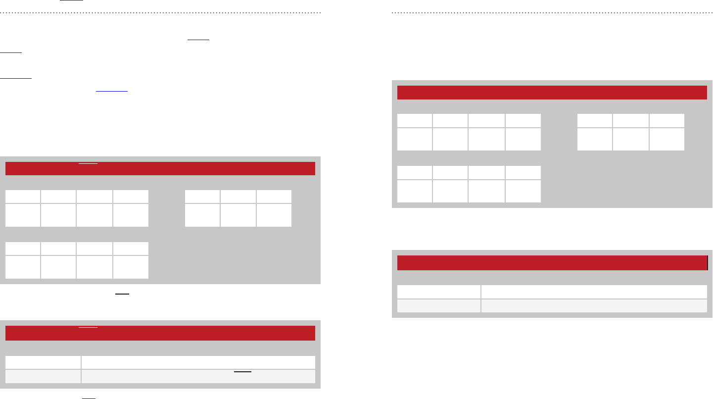
– – – –
70 71
CMDHOLD - CMD Halts Traffic
Volatile Address = 0x6E; Non-Volatile Address = 0x23
A CMDHOLD register setting of 0x01 causes the module to store incoming
RF traffic (up to the RF buffer size) while the CMD line is low. When the
CMD line is returned high, the module outputs all buffered data. A register
value of 0 allows received bytes to be output on the UART immediately with
CRESP high to indicate that the bytes are received data. See Using the
Command Response (CRESP) Line section for details. This register setting
is overridden when PKOPT:RXPKT=1.
Figure 70 shows examples of the commands and Figure 71 shows the
available values.
Figure 70: HumPROTM Series Transceiver CMD Halts Traffic Command and Response
HumPROTM Series CMD Halts Traffic Register Settings
V Mode
0x00 Disable Halt (received data is sent to the UART immediately)
0x01 Enable Halt (received data is sent when the CMD line is high)
Figure 71: HumPROTM Series CMD Halts Traffic Register Settings
HumPROTM Series CMD Halts Traffic
Read Command Read Response
Header Size Escape Address ACK Address Value
0xFF 0x02 0xFE 0x6E
0x23 0x06 0x6E
0x23 V
Write Command
Header Size Address Value
0xFF 0x02 0x6E
0x23 V
COMPAT - Compatibility Mode
Volatile Address = 0x70; Non-Volatile Address = 0x25
Compatibility mode allows the HumPROTM Series modules to communicate
with the 250 Series modules. Please see the Compatibility Mode section
for more details. Figure 72 shows examples of the commands and Figure
73 shows the available values.
Figure 72: HumPROTM Series Transceiver Compatibility Mode Command and Response
HumPROTM Series Compatibility Mode
Read Command Read Response
Header Size Escape Address ACK Address Value
0xFF 0x02 0xFE 0x70
0x25 0x06 0x70
0x25 V
Write Command
Header Size Address Value
0xFF 0x02 0x70
0x25 V
HumPROTM Series Compatibility Mode Register Settings
V Mode
0x00 Enable 250 Series Compatibility Mode
0x02 Enable normal Addressing Operation
Figure 73: HumPROTM Series Compatibility Mode Register Settings

– – – –
72 73
AUTOADDR - Auto Addressing
Volatile Address = 0x71; Non-Volatile Address = 0x26
When the AUTOADDR feature is enabled, the module reads the Source
Address from a received packet and uses it to fill the Destination Address
registers (UDESTID or DESTDSN, depending on the addressing mode of
the received message). This ensures that a response is sent to the device
that transmitted the original message. The response ADDMODE should be
the same as ADDMODE used to send the original message.
The non-volatile register only uses the lower 4 bits to configure the
automatic addressing. The upper 4 bits are not used.
The volatile register is split in half with the lower 4 bits configuring the
automatic addressing, the same as the non-volatile register. The upper 4
bits indicate the type of packet that was last received. This indication is the
same as the Addressing Mode register setting. These bits are not used by
the module and are only written by the module after successfully receiving
a packet.
As an example, if AUTOADDR is set to 0x0F (Any Auto Address) and a
DSN packet is received from another module, then AUTOADDR reads back
as 0x4F. The lower 4 bits (0xF) indicate that the module is set to any auto
address (0xF). The upper 4 bits (0x4) indicate that the packet that was just
received was a DSN Addressing Mode packet.
Figure 74 summarizes the configuration values for the lower 4 bits of the
register.
Figure 75 shows the Addressing Mode values that the module writes to the
upper 4 bits after successfully receiving a packet.
HumPROTM Series Auto Addressing Register Settings
Auto Address Value Meaning Action
0x00 Auto Addressing disabled Destination Registers not
populated
0x04 DSN Auto Address Auto-populates DSN Address
Destination Register Only
0x06 User Auto Address Mode Auto-populates User Address
Destination Register
0x07 Extended User Auto Address
Mode
Auto-populates Extended User
Address Destination Register
0x0F Any Auto Address Mode
Auto-populates DSN
Destination or User Address
Destination, depending on the
received message type.
Figure 74: HumPROTM Series Transceiver Auto Addressing Register Settings
HumPROTM Series Auto Addressing Mode Indicator
Addressing Mode Meaning
0x4 DSN Addressing Mode
0x6 User Addressing Mode
0x7 Extended User Addressing Mode
Figure 75: HumPROTM Series Transceiver Auto Addressing Mode Indicator
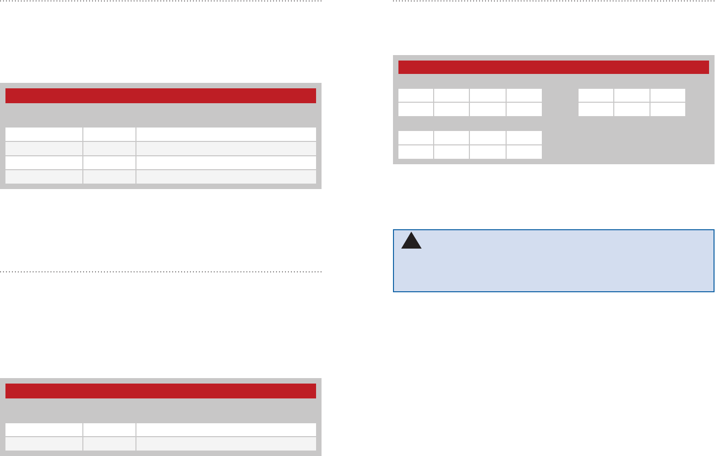
– – – –
74 75
CRSSI - Carrier Sense Minimum RSSI
Non-Volatile Address = 0x3F
This value is the minimum RSSI that causes the module to wait for a
clear channel when CSMA is enabled. Figure 78 shows examples of the
commands.
The value is a negative number in two’s complement from -128 (0x80) to -1
(0xff). The default value is -70dBm.
HumPROTM Series DSN Registers
Name Non-Volatile
Address Description
MYDSN3 0x34 MSB of the serial number
MYDSN2 0x35 Byte 2 of the serial number
MYDSN1 0x36 Byte 1 of the serial number
MYDSN0 0x37 LSB of the serial number
Figure 76: HumPROTM Series DSN Registers
HumPROTM Series Customer ID Registers
Name Non-Volatile
Address Description
CUSTID1 0x39 MSB of the customer ID
CUSTID0 0x3A LSB of the customer ID
Figure 77: HumPROTM Series Transceiver Customer ID Registers
MYDSN - Local Device Serial Number
Non-Volatile Address = 0x34-0x37
These registers contain the factory-programmed read-only Device Serial
Number. This address is unique for each module and is included in all
packet types as a unique origination address.
Figure 76 shows the Device Serial Number registers.
CUSTID - Customer ID
Non-Volatile Address = 0x39-0x3A
These registers contain the factory-programmed customer ID. A unique
value is assigned to a specific customer and that value is programmed
into that customer’s modules. The unencrypted User and Extended User
Addressing modes use these bytes as part of the addressing. The unique
value ensures that the custom modules will not communicate with any
other systems. Contact Linx for details. Figure 77 shows the Customer ID
registers.
HumPROTM Series Carrier Sense Minimum RSSI
Read Command Read Response
Header Size Escape Address ACK Address Value
0xFF 0x02 0xFE 0x3F 0x06 0x3F V
Write Command
Header Size Address Value
0xFF 0x02 0x3F V
Figure 78: HumPROTM Series Transceiver Carrier Sense Minimum RSSI Command and Response
Warning: The CRSSI value can have a significant impact on the
performance of the module. Setting it too low could prevent the module
from ever transmitting. Setting it too high can result in transmission
collisions. Care must be taken if this value is adjusted.
!
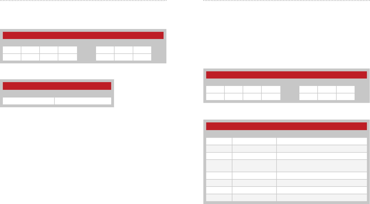
– – – –
76 77
RELEASE - Release Number
Non-Volatile Address = 0x78
This register contains a number designating the firmware version and
hardware platform. Figure 79 shows examples of the commands and
Figure 80 lists current releases to date.
A more detailed firmware version is available for versions 0x20 and above in
the FWVER register.
HumPROTM Series Release Number Register Settings
V Release Number
0x20 HUM-900-PRO
HumPROTM Series Release Number
Read Command Read Response
Header Size Escape Address ACK Address Value
0xFF 0x02 0xFE 0x78 0x06 0x78 V
Figure 79: HumPROTM Series Transceiver Release Number Command and Response
Figure 80: HumPROTM Series Transceiver Release Number Register Settings
EXCEPT - Exception Code
Volatile Address = 0x79
The module has a built-in exception engine that can notify the host
processor of an unexpected event. If an exception occurs, the exception
code is stored in this register. Reading from this register clears the
exception and resets the EX line. If an exception occurs before the previous
exception code is read, the previous value is overwritten. Please see the
Exception Engine section for more details.
Figure 81 shows examples of the commands and Figure 82 shows the
available values.
Figure 81: HumPROTM Series Transceiver Exception Code Command and Response
HumPROTM Series Transceiver Exception Codes
V Exception Name Description
0x08 EX_BUFOVFL Internal UART buffer overflowed.
0x09 EX_RFOVFL Internal RF packet buffer overflowed.
0x13 EX_WRITEREGFAILED Attempted write to register failed.
0x20 EX_NOACK Acknowledgement packet not received after
maximum number of retries.
0x40 EX_BADCRC Bad CRC detected on incoming packet.
0x42 EX_BADHEADER Bad CRC detected in packet header.
0x43 EX_BADSEQID Sequence ID was incorrect in ACK packet.
0x44 EX_BADFRAMETYPE Unsupported frame type specified.
Figure 82: HumPROTM Series Transceiver Exception Codes
HumPROTM Series Exception Code
Read Command Read Response
Header Size Escape Address ACK Address Value
0xFF 0x02 0xFE 0x79 0x06 0x79 V

– – – –
78 79
PRSSI - Last Good Packet RSSI
Volatile Address = 0x7B
This register holds the received signal strength in dBm of the last
successfully received packet. A successful packet reception is one that
causes payload data to be output on the UART interface. The value in this
register is overwritten each time a new packet is successfully processed.
The register value is an 8-bit signed integer representing the RSSI in dBm.
It is accurate to ±3dB.
ARSSI - Ambient RSSI
Volatile Address = 0x7C
This register returns the ambient receive signal strength on the current
channel in dBm. The signal strength is measured as soon as the command
is received. The register value is an 8-bit signed integer representing the
RSSI in dBm. It is accurate to ±3dB.
Figure 83: HumPROTM Series Transceiver Last Good Packet RSSI Command and Response
Figure 84: HumPROTM Series Transceiver Ambient RSSI Command and Response
HumPROTM Series Last Good Packet RSSI
Read Command Read Response
Header Size Escape Address ACK Address Value
0xFF 0x02 0xFE 0x7B 0x06 0x7B V
HumPROTM Series Ambient RSSI
Read Command Read Response
Header Size Escape Address ACK Address Value
0xFF 0x02 0xFE 0x7C 0x06 0x7C V
FWVER - Firmware Version
Non-Volatile Address = 0xC0 - 0xC3
These read-only registers contain the firmware version number currently
on the module. Each byte is a hexadecimal value: 12 03 01 00 indicates
version 18.3.1.0. Each register byte is read separately. Figure 85 shows the
Firmware Version registers.
HumPROTM Series Firmware Version Registers
Name Non-Volatile
Address Description
FWVER3 0xC0 Major version number
FWVER2 0xC1 Minor version number
FWVER1 0xC2 Incremental version number
FWVER0 0xC3 Suffix
Figure 85: HumPROTM Series Firmware Version Registers
Note: Encryption is implemented on modules with FWVER3 = 2 and
higher.

– – – –
80 81
NVCYCLE - Non-Volatile Erase Cycles
Non-Volatile Address = 0xC4-0xC5
These read-only non-volatile registers contain the number of lifetime erase
cycles performed for the non-volatile memory. The minimum lifetime erases
is 2,000 erase cycles. Beyond this the erases may not be complete and the
module’s operation can become unpredictable.
Between 13 and 158 non-volatile write operations can be made before
an erase cycle is necessary. Writing the registers from lowest to highest
address maximizes the number of write operations.
It is recommended to write the desired default values to non-volatile
memory and use the volatile registers for values that change frequently.
These registers show the total number of erase cycles that have occurred.
This gives an indication of the remaining life expectancy of the memory.
Figure 86 shows the Non-Volatile Erase Cycles registers.
HumPROTM Series Non-Volatile Erase Cycles Registers
Name Non-Volatile
Address Description
NVCYCLE1 0xC4 MSB of the number of erase cycles
NVCYCLE0 0xC5 LSB of the number of erase cycles
Figure 86: HumPROTM Series Non-Volatile Erase Cycles Registers
LSTATUS - Output Line Status
Volatile Address = 0xC6
This register contains the logic states of the output indicator lines, providing
information to the host processor while using fewer GPIO lines.
Each bit in the byte that is returned by the read represents the logic state
of one of the output indicator lines. Figure 88 shows which line each bit
represents.
Figure 87: HumPROTM Series Transceiver Output Line Status Command and Response
HumPROTM Series Output Line Status
Read Command Read Response
Header Size Escape Escape Address ACK Address Value
0xFF 0x03 0xFE 0xFE 0x46 0x06 0xC6 LSTATUS
HumPROTM Series Output Line Status LSTATUS Values
LSTATUS Bit Line Status
0 EX – Exception, 1 = exception has occurred
1 PA_EN – PA Enable, 1 = the transmitter is active
2 LNA_EN – LNA Enable, 1 = the receiver is active
3 CTS – Clear To Send, 1 = incoming data buffer near full
4 MODE_IND – Mode Indicator, 1 = RF data transfer is active (TX or RX)
5 BE – Buffer Empty, 1 = UART buffer is empty
6 Reserved
7 Reserved
Figure 88: HumPROTM Series Output Line Status LSTATUS Values
– – – –
82 83
CMD - Command Register
Volatile Address = 0xC7
This volatile write-only register is used to issue special commands.
Value V is chosen from among the options in Figure 90.
The Send Packet command starts data transmission. Operation differs
depending on whether option TXPKT is set in the PKTOPT register.
• TXPKT = 0; this command operates the same as a data timeout with
DATATO. All waiting data, up to the maximum allowed in the remaining
channel time, is transmitted.
• TXPKT = 1; this command marks the end of an explicit packet in
the outgoing buffer. All bytes in the packet are transmitted together.
Following bytes are sent in the next packet. The max packet length is
192 bytes. Multiple packets can be queued with this command.
HumPROTM Series CMD Values
CMD Value Operation
0x1 SENDP – Send Packet
0x2 GETPH – Get Packet Header
0x3 GETPD – Get Packet Data
0x4 GETPHD – Get Packet Header and Data
0x5 CLRRXP – Clear Received Packet
0x6 CLROB – Clear Outbound Buffer
0x07 CLRIB – Clear Input Buffer
0x10 JOINCTL – Join Process Control
0x11 WRKEY – Write Key
0x12 CLRKEY – Clear Key
0x13 RLDKEY – Reload Key
0x20 0xAA 0xBB NVRESET – Reset non-volatile registers to factory default
Figure 89: HumPROTM Series Transceiver Command Register Command and Response
HumPROTM Series Command Register
Write Command
Header Size Escape Address Value
0xFF 0x03 0xFE 0x47 V
Figure 90: HumPROTM Series Command Register Values
The Get Packet Header command returns the received packet header
using a received packet transfer cycle (see the Receiving Packets section).
The header is discarded after transfer. This command is normally issued
after receiving an RXWAIT exception. The packet data can be read after
completion of the header transfer. If the data is not read before this
command is issued a second time, then the data is discarded and the
header for the following packet is returned. A NAK response is returned if
option RXPKT is disabled in the PKTOPT register or the previous GETPx
command was not completed.
The Get Packet Data command returns the received packet data using a
received packet transfer cycle. If the packet header is not read first, then
it is discarded. The packet data is then discarded after transfer. A NAK
response is returned if option RXPKT is disabled in the PKTOPT register or
the previous GETPx command was not completed.
The Get Packet Header and Data command returns the received packet
header, followed by the packet data using a received packet transfer
cycle. The packet is discarded after transfer. A NAK response is returned
if option RXPKT is disabled in the PKTOPT register or the previous GETPx
command was not completed.
The Clear Received Packet command removes the next unread packet
from the RF incoming queue if RXPKT is enabled in the PKTOPT register.
If the packet header was read but not the data, this command causes
the data to be discarded. Although not required before reading the next
packet’s header, it frees buffer space for more or longer messages.
If a previous GETPx command did not deliver all the associated data,
this command removes the undelivered data and terminates the previous
GETPx command.
If option RXPKT is disabled this command discards all received data which
has not been delivered.
The Clear Outbound Buffer command cancels any transmission in
progress and clears the buffer of data to be transmitted.
The Clear Input Buffer command discards all RF-received bytes and
clears the EX_RXWAIT flag.

– – – –
84 85
The Join Process Control command allows the software to initiate or stop
the secure JOIN process. It has the following subcommands.
These operations are equivalent to the push-button initiated operation.
If a JOIN operation is started by the serial command (CMD:JOINCTL[2]),
push-button operation is ignored until the JOIN operation finishes.
Register write operations are inhibited when a JOIN process is active
except that a Halt JOIN command is never inhibited. A Halt JOIN operation
completes before the ACK is sent.
When the JOIN operation is started the KEYRCV flag in the SECOPT
register determines whether the module is a master or slave and whether
a key can be sent or changed. The JOIN process uses and modifies the
non-volatile address registers.
The Write Key command writes a 16-byte AES key to the selected key
register. As with most of the registers, the encryption key has both volatile
and non-volatile registers. The volatile register is used during run time, but
is lost on a power cycle or reset. When the module powers up, the volatile
register is loaded from the non-volatile register. This makes the non-volatile
register value the default on power-up.
The key value of all zero bytes is reserved as a “no key” indication.
Figure 92 shows the command for writing the AES key to the module.
If KeyN is 0x01, the command writes to the volatile key register. If it is 0x02,
it writes to the non-volatile key register.
HumPROTM Series JOINCTL Subcommand Values
Subcommand Value Operation
0 Halt JOIN operation
1Generate a random network key and address. This sets the
module as the network master (SECOPT:KEYRCV=0)
2 Perform the JOIN operation with another module
Figure 91: HumPROTM Series JOINCTL Subcommand Values
Figure 92: HumPROTM Series Transceiver Write Key Command
HumPROTM Series Write Key Command
Write Command
Header Size Escape Address Value KeyN Key0 ... Key15
0xFF Size 0xFE 0x47 0x11 KeyN Key0 ... Key15
The Clear Key command sets the selected key to all zeros. Figure 93
shows the structure of this command.
If KeyN is 0x01, the command writes to the volatile key registers. If it is
0x02, it writes to the non-volatile key registers.
The Reload Key command copies the key in non-volatile memory (NKN)
to the volatile location (NKV). This allows a sophisticated system to change
the keys during operation and quickly revert back to the default key.
The Non-volatile Reset command (FF 07 FE 47 20 FE 2A FE 3B) sets
all non-volatile registers to their default values. When the configuration is
reset, the following message, shown in quotes, is sent out the UART at the
current baud rate, then the module is reset, similar to a power cycle:
“\r\nConfiguration Reset\r\n”.
This reset can also be done by toggling the PB line as described in the
Restore Factory Defaults section.
Figure 93: HumPROTM Series Transceiver Clear Key Command
HumPROTM Series Clear Key Command
Write Command
Header Size Escape Address Value KeyN
0xFF 0x04 0xFE 0x47 0x12 KeyN

– – – –
86 87
SECSTAT - Security Status
Volatile Address = 0xC9
This volatile read-only register provides status of the security features.
The command returns a single byte. Figure 95 shows the meanings of the
bits in the returned value byte.
Figure 94: HumPROTM Series Transceiver Security Status Command and Response
HumPROTM Series Security Status
Read Command Read Response
Header Size Escape Escape Address ACK Address Value
0xFF 0x03 0xFE 0xFE 0x49 0x06 0xC9 V
HumPROTM Series Security Status Value
Bit Status
0 Reserved
10 = No volatile key is set
1 = A volatile key is set
20 = No non-volatile key is set
1 = A non-volatile key is set
3 Reserved
4 Reserved
5 Reserved
6 Reserved
7 Reserved
Figure 95: HumPROTM Series Security Status Values
JOINST - Join Status
Volatile Address = 0xCA
This volatile read-only register shows the current or previous state of join
activity since the module was last reset.
The command returns a single byte. Figure shows the meanings of the
returned value byte.
Figure 96: HumPROTM Series Transceiver Join Status Command and Response
HumPROTM Series Join Status
Read Command Read Response
Header Size Escape Escape Address ACK Address Value
0xFF 0x03 0xFE 0xFE 0x4A 0x06 0xCA V
HumPROTM Series Join Status Value
Bit Status
0 - 5
Last Join Result (decimal):
Last Operation Successful
0: Module unpaired since restart
1: New key generated
2: Successfully sent address to another unit
3: Successfully sent address and key to another unit
4: Successfully obtained key from master
5: Successfully obtained address from master
6: Successfully obtained key and address from master
Last Operation Failed
10: Fail: operation canceled
11: Fail: timeout
12: Fail: too many joining units
13: Fail: Assignment message didn’t contain key
14: Fail: Master has no key to send when SECOPT:PSHARE=1
15: Fail: Master has no address to send
16: Fail: Inconsistent Network Address Registers USRC, UMASK, LASTNETAD
Current Operation
32: Detecting PB sequence
33: Waiting for joining unit
34: Another joining unit detected. Joining is in progress.
6JOINACT – MODE_IND is active with pairing status, serial write operations are
inhibited
Figure 97: HumPROTM Series Transceiver Join Status Value

– – – –
88 89
EEXFLAG - Extended Exception Flags
Volatile Address = 0xCD - 0xCF
These volatile registers contain flags for various events. Similar to the
EXCEPT register, they provide a separate bit for each exception.
When an exception occurs, the associated bit is set in this register. If the
corresponding bit in the EEXMASK is set and EXMASK is zero, the EX
status line is set. Reading an EEXFLAG register does not clear the register.
Writing to an EEXFLAG register causes the register to be set to the
BIT_AND(current_value, new_value). This provides a way of clearing bits
that have been serviced without clearing a bit that has been set since the
flag register was read. This prevents a loss of notification of an exception.
Register bits can only be cleared, not set, from the write command though
some flags are also cleared internally.
Flag EX_TXDONE is set when a data packet has been transmitted. If the
packet was sent with acknowledgement enabled, this flag indicates that
the acknowledgment has also been received. It is cleared by writing a zero
bit to EX_TXDONE in the register.
Flag EX_RXWAIT is 1 when there are buffered incoming data bytes which
have not been sent to the UART. It is cleared by reading or discarding all
data bytes.
Flag EX_UNENCRYPT is 1 when a received packet is not encrypted. This
can only occur when SECOPT:EN_UNC=1.
Flag EX_SEQDEC is 1 when a received encrypted packet has a smaller
sequence number than the previously received packet. Possible causes
are an attempt to replay a previous message by an attacker, receiving a
message from a different transmitter or restarting the transmitter.
Figure 98: HumPROTM Series Transceiver Extended Exception Code Registers
HumPROTM Series Extended Exception Flags Registers
Name Volatile
Address Description
EEXMASK2 0xCD Byte 2 of the extended exception flags
EEXMASK1 0xCE Byte 1 of the extended exception flags
EEXMASK0 0xCF LSB of the extended exception flags
HumPROTM Series Transceiver Extended Exception Codes
Bit Exception Name Description
EEXFLAG0 (0xCF)
0 EX_BUFOVFL Internal UART buffer overflowed.
1 EX_RFOVFL Internal RF packet buffer overflowed.
2 EX_WRITEREGFAILED Attempted write to register failed.
3 EX_NOACK Acknowledgement packet not received after
maximum number of retries.
4 EX_BADCRC Bad CRC detected on incoming packet.
5 EX_BADHEADER Bad CRC detected in packet header.
6 EX_BADSEQID Sequence ID was incorrect in ACK packet.
7 EX_BADFRAMETYPE Unsupported frame type specified.
EEXFLAG1 (0xCE)
0 EX_TXDONE A data packet has been transmitted.
1 EX_RXWAIT Received data bytes are waiting to be read.
2 EX_UNENCRYPT Received packet was not encrypted. This can
only occur when SECOPT: EN_UNENC=1.
3 EX_SEQDEC Received encrypted packet sequence number is
less than previous
4 EX_SEQSKIP Received encrypted sequence number is more
than one higher the previous sequence number
5 - 7 Reserved
EEXFLAG2 (0xCD)
0 - 7 Reserved
Figure 99: HumPROTM Series Transceiver Extended Exception Codes
Flag EX_SEQSKIP is 1 when a received encrypted packet has a sequence
number that is more than one higher than the previously received packet.
Possible causes are an attempt to replay a previous message by an
attacker, receiving a message from a different transmitter or restarting the
transmitter.

– – – –
90 91
PKTOPT - Packet Options
Volatile Address = 0xD3; Non-Volatile Address = 0x83
This register selects options for transferring packet data.
Each bit in the register sets an option as shown in Figure 101.
The TXPKT option allows the module to transmit data in explicit packets.
• TXPKT = 0 (default); a packet transmission is enabled when the
number of waiting bytes reaches BCTRIG bytes, the time since the
last received byte exceeds DATATO ms, the number of waiting bytes
exceeds the number that can be sent within the remaining slot time, or
a Send Packet command is written to the CMD register.
• TXPKT = 1; all bytes written to the module are held until a SENDP
command is written to the CMD register or the CMD line is lowered
with TXnCMD = 1. The DATATO or BCTRIG conditions are ignored with
this option. The transmitted packet consists of the bytes in the buffer
at the time a packet is triggered, even if more data bytes are received
before the packet can be sent.
Figure 100: HumPROTM Series Transceiver Packet Options Command and Response
HumPROTM Series Packet Options
Read Command Read Response
Header Size Escape Address ACK Address Value
0xFF 0x02 0xFE 0xD3
0x83 0x06 0xD3
0x83 V
Write Command
Header Size Address Value
0xFF 0x02 0xD3
0x83 V
HumPROTM Series Transceiver Packet Option Codes
Bit Name Description
0 TXPKT Packet Transmit
1 TXnCMD Transmit when nCMD Lowered
2 RXPKT Packet Receive
3 RXP_CTS Use CTS for RXPKT Transfer
4 - 7 Reserved Reserved
Figure 101: HumPROTM Series Transceiver Packet Option Codes
Multiple outgoing packets can be buffered. Changing this option clears the
incoming buffer, losing un-transmitted or unacknowledged data.
When TXnCMD is 1, lowering the CMD line has the same effect as writing
the SENDP command to the CMD register, triggering buffered data to be
transmitted. Packet grouping is affected by option TXPKT. The minimum
low time on the CMD line to terminate the packet is given in the Electrical
Specifications.
When RXPKT is 1, incoming packets are held until a GETPH, GETPD, or
GETPHD command is written to the CMD register. Transfer uses a Packet
Receive transfer. The CMDHOLD setting has no effect.
When RXPKT is 0, incoming UART data is delivered without headers. The
data flow is controlled by the CMDHOLD setting.
When RXP_CTS is 1, the CTS line is used for the status line during a
Packet Receive transfer and not for controlling data flow into the module.
When it is 0, CTS is used for flow control and CRESP is used for the status
line.

– – – –
92 93
SECOPT - Security Options
Volatile Address = 0xD4; Non-Volatile Address = 0x84
This register selects options for security features.
Each bit in the register sets an option as shown in Figure 103.
When PB_RESET is 1 the Factory Reset function is enabled from the PB
input. This allows a user to reset the module configurations back to the
factory defaults with 4 short presses and a 3 second hold of a button
connected to the PB input.
When PSHARE is 1 the Share Network Key function is enabled during
the JOIN process. This allows a master unit to share the encryption key it
created.
Figure 102: HumPROTM Series Transceiver Packet Options Command and Response
HumPROTM Series Security Options
Read Command Read Response
Header Size Escape Escape Address ACK Address Value
0xFF 0x03 0xFE 0xFE 0x54
0x04 0x06 0xD4
0x84 V
Write Command
Header Size Escape Address Value
0xFF 0x03 0xFE 0x54
0x04 V
HumPROTM Series Transceiver Security Option Codes
Bit Name Description
0 PB_RESET Permit factory reset from PB input sequence
1 PSHARE Permit key sharing
2 PGKEY Permit clearing key and changing key
3 CHGADDR Permit changing an address
4 KEYRCV 1: Receive key and address during JOIN operation (slave)
0: Send key and address during JOIN operation (master)
5 EN_UNENC Enable receiving unencrypted packets
6 Reserved Reserved
7 EN_CHANGE Enable changes to security options
Figure 103: HumPROTM Series Transceiver Security Option Codes
When PGKEY is 1 the JOIN process is allowed to change or clear the
network key. The key can always be changed through serial commands.
When CHGADDR is 1 the JOIN process is allowed to generate a random
network address if the module is a master unit. If the module is a slave unit
it is allowed to accept an address assignment from the master unit.
When KEYRCV is 1 the module is set to receive a network key from a
master unit and act as a slave. When it is 0, the module is set to act as a
master and send a network key and assign an address to the slave unit.
In order for this bit to change from 1 to 0, the network key must be cleared,
preventing slave units from being manipulated to transmit the key. This bit
is cleared by the GENERATE_KEY push-button function.
When EN_UNENC is 1 the module accepts unencrypted packets. If this bit
is 0, unencrypted received packets are ignored.
When EN_CHANGE is 1, changes to the SECOPT register bits 0-3, 5-7 are
permitted from serial commands. Clearing this bit prevents any of these
bits from changing without resetting the module to factory default, which
clears the network key.
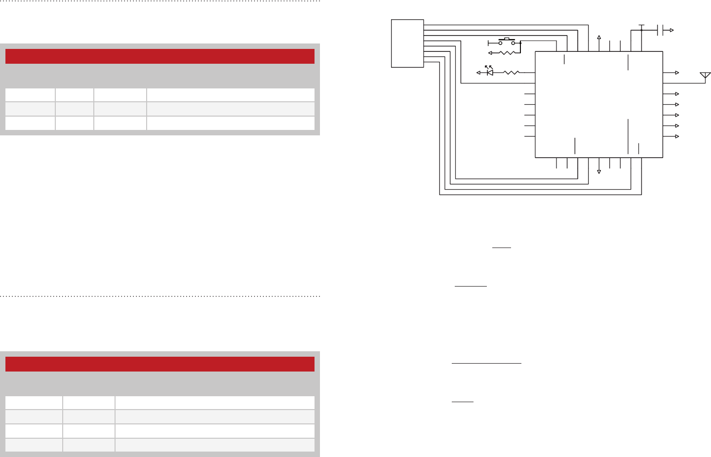
– – – –
94 95
Typical Applications
Figure 106 shows a typical circuit using the HumPROTM Series transceiver.
An external microcontroller provides data and configuration commands.
Its UART (TXD, RXD) is connected to the module’s UART (CMD_DATA_IN,
CMD_DATA_OUT). The CTS line is monitored for flow control. GPIOs on
the microcontroller are connected to lines on the module:
It monitors the CRESP line to know when the data coming out of the
module is transmitted data or a response to a command.
It monitors the EX line to know if there is an error. This line may be
connected to an interrupt line for faster response.
It controls the POWER_DOWN line to place the module into a low power
state.
It controls the CMD line to toggle between configuration commands and
data to be transmitted over the air.
The MODE_IND line is connected to an LED for visual indication that the
module is active.
The PB line is connected to a pushbutton that takes the line to VCC when
it is pressed. A resistor pulls the line to ground when the button is not
pressed.
GND 17
VCC 21
GND 18
RESET 22
LNA_EN 23
PA_EN 24
CMD_DATA_OUT 26
CMD_DATA_IN 27
CTS 28
PB 29
NC
2
GND 25
NC
1
MODE_IND
30
BE
31
NC
32
NC
3
NC
4
ANT 19
GND 20
NC
5
NC
6
CRESP
7
EX
8
NC
10
NC
11
POWER_DOWN
12
CMD
13
GND
9
GND 16
GND 15
GND 14
GND
GND
GND
GND
GND
GND
GND
GND
GND
VCC
GND
GPIO
GPIO
INT/GPIO
GPIO
GPIO
GPIO
TXD
RXD
µVCC
GND
Figure 106: HumPROTM Series Transceiver Basic Application Circuit
EEXMASK - Extended Exception Mask
Volatile Address = 0x80-0x82; Non-Volatile Address = 0xD0-0xD2
These registers contain a mask for the events in EEXFLAG, using the same
offset and bit number.
To use this value, register EXMASK must be zero. If EXMASK is non-zero,
this register has no effect on the EX line.
When an exception bit is set in EEXFLAG, the corresponding EEXMASK
bit is set, and EXMASK is zero, the EX status line is set, otherwise the
EX line is reset. Mask bits for unassigned flags should be zero for future
compatibility.
LASTNETAD - Last Network Address Assigned
Non-Volatile Address = 0x8C-0x8F
These bytes contain the last address assigned using the JOIN process.
When a new unit joins the network, it is assigned the next address and this
value is incremented in the master. It is initially set to the master address
when a network key is generated.
Figure 104: HumPROTM Series Transceiver Extended Exception Mask Registers
HumPROTM Series Extended Exception Mask Registers
Name Volatile
Address
Non-Volatile
Address Description
EEXMASK2 0x80 0xD0 Byte 2 of the extended exception mask
EEXMASK1 0x81 0xD1 Byte 1 of the extended exception mask
EEXMASK0 0x82 0xD2 LSB of the extended exception mask
Figure 105: HumPROTM Series Transceiver Extended Exception Mask Registers
HumPROTM Series Extended Exception Mask Registers
Name Non-Volatile
Address Description
LASTNETAD3 0x8C MSB of the last network address assigned
LASTNETAD2 0x8D Byte 2 of the last network address assigned
LASTNETAD1 0x8E Byte 1 of the last network address assigned
LASTNETAD0 0x8F LSB of the last network address assigned

– – – –
96 97
Usage Guidelines for FCC Compliance
The pre-certified versions of the HumPROTM Series module
(HUM-900-PRO-UFL and HUM-900-PRO-CAS) are provided with an FCC
and Industry Canada Modular Certification. This certification shows that
the module meets the requirements of FCC Part 15 and Industry Canada
license-exempt RSS standards for an intentional radiator. The integrator
does not need to conduct any further testing under these rules provided
that the following guidelines are met:
• An approved antenna must be directly coupled to the module’s U.FL
connector through an approved coaxial extension cable or to the
module’s castellation pad using an approved reference design and
PCB layer stack.
• Alternate antennas can be used, but may require the integrator to
perform certification testing.
• The module must not be modified in any way. Coupling of external
circuitry must not bypass the provided connectors.
• End product must be externally labeled with “Contains FCC ID:
OJM900MCA / IC: 5840A-900MCA”.
• The end product’s user’s manual must contain an FCC statement
equivalent to that listed on page 97 of this data guide.
• The antenna used for this transceiver must not be co-located or
operating in conjunction with any other antenna or transmitter.
• The integrator must not provide any information to the end-user on
how to install or remove the module from the end-product.
Any changes or modifications not expressly approved by Linx Technologies
could void the user’s authority to operate the equipment.
Additional Testing Requirements
The HUM-900-PRO-UFL and HUM-900-PRO-CAS have been tested
for compliance as an intentional radiator, but the integrator is required to
perform unintentional radiator testing on the final product per FCC sections
15.107 and 15.109 and Industry Canada license-exempt RSS standards.
Additional product-specific testing might be required. Please contact
the FCC or Industry Canada regarding regulatory requirements for the
application. Ultimately is it the integrator’s responsibility to show that their
product complies with the regulations applicable to their product.Versions
other than the -UFL and -CAS have not been tested and require full
compliance testing in the end product as it will go to market.
Information to the user
The following information must be included in the product’s user manual.
FCC / IC NOTICES
This product contains FCC ID: OJM900MCA / IC: 5840A-900MCA.
This device complies with Part 15 of the FCC rules and Industry Canada
license-exempt RSS standards. Operation of this device is subject to the
following two conditions:
1. This device may not cause harmful interference, and
2. this device must accept any interference received, including interference that
may cause undesired operation.
This equipment has been tested and found to comply with the limits for a Class
B digital device, pursuant to Part 15 of the FCC Rules. These limits are designed
to provide reasonable protection against harmful interference in a residential
installation. This equipment generates, uses and can radiate radio frequency
energy and, if not installed and used in accordance with the instructions,
may cause harmful interference to radio communications. However, there is
no guarantee that interference will not occur in a particular installation. If this
equipment does cause harmful interference to radio or television reception, which
can be determined by turning the equipment off and on, the user is encouraged
to try to correct the interference by one or more of the following measures:
• Reorient or relocate the receiving antenna.
• Increase the separation between the equipment and receiver.
• Connect the equipment into an outlet on a circuit different from that to which
the receiver is connected.
• Consult the dealer or an experienced radio/TV technician for help.
Any modifications could void the user’s authority to operate the equipment.
Le présent appareil est conforme aux CNR d’Industrie Canada applicables
aux appareils radio exempts de licence. L’exploitation est autorisée aux deux
conditions suivantes:
1. l’appareil ne doit pas produire de brouillage, et
2. ’utilisateur de l’appareil doit accepter tout brouillage radioélectrique subi,
même si le brouillage est susceptible d’en compromettre le fonctionnement.

– – – –
98 99
Product Labeling
The end product containing the HUM-900-PRO-UFL or
HUM-900-PRO-CAS must be labeled to meet the FCC and IC product
label requirements. It must have the below or similar text:
Contains FCC ID: OJM900MCA / IC: 5840A-900MCA
The label must be permanently affixed to the product and readily visible to
the user. ‘‘Permanently affixed’’ means that the label is etched, engraved,
stamped, silkscreened, indelibly printed, or otherwise permanently marked
on a permanently attached part of the equipment or on a nameplate of
metal, plastic, or other material fastened to the equipment by welding,
riveting, or a permanent adhesive. The label must be designed to last
the expected lifetime of the equipment in the environment in which the
equipment may be operated and must not be readily detachable.
FCC RF Exposure Statement
To satisfy RF exposure requirements, this device and its antenna must
operate with a separation distance of at least 20cm from all persons and
must not be co-located or operating in conjunction with any other antenna
or transmitter.
Antenna Selection
Under FCC and Industry Canada regulations, the HUM-900-PRO-UFL and
HUM-900-PRO-CAS radio transmitters may only operate using an antenna
of a type and maximum (or lesser) gain approved for the transmitter by
the FCC and Industry Canada. To reduce potential radio interference
to other users, the antenna type and its gain should be so chosen that
the equivalent isotropically radiated power (e.i.r.p.) is not more than that
necessary for successful communication.
The HUM-900-PRO-UFL and HUM-900-PRO-CAS radio transmitters
have been approved by the FCC and Industry Canada to operate with the
antenna types listed in Figure 107 with the maximum permissible gain and
required antenna impedance for each antenna type indicated. Antenna
types not included in this list, having a gain greater than the maximum gain
indicated for that type, are strictly prohibited for use with this device.
Conformément à la réglementation d’Industrie Canada, le présent émetteur
radio peut fonctionner avec une antenne d’un type et d’un gain maximal
(ou inférieur) approuvé pour l’émetteur par Industrie Canada. Dans le but
de réduire les risques de brouillage radioélectrique à l’intention des autres
utilisateurs, il faut choisir le type d’antenne et son gain de sorte que la
puissance isotrope rayonnée équivalente (p.i.r.e.) ne dépasse pas l’intensité
nécessaire à l’établissement d’une communication satisfaisante.
Le présent émetteur radio (HUM-900-PRO-UFL, HUM-900-PRO-CAS)
a été approuvé par Industrie Canada pour fonctionner avec les types
d’antenne énumérés la Figure 107 et ayant un gain admissible maximal
et l’impédance requise pour chaque type d’antenne. Les types d’antenne
non inclus dans cette liste, ou dont le gain est supérieur au gain maximal
indiqué, sont strictement interdits pour l’exploitation de l’émetteur.
Figure 107: HumPROTM Series Transceiver Approved Antennas
Antennas / Antennes
Linx Part Number
Référence Linx Type Gain Impedance
Impédance Valid For
Tested Antennas
ANT-916-CW-QW ¼ Wave Whip 1.8dBi 50Ω–CAS
ANT-916-CW-HW ½ Wave Dipole Helical 1.2dBi 50ΩBoth
ANT-916-PW-LP ¼ Wave Whip 2.4dBi 50Ω–CAS
ANT-916-PW-QW-UFL ¼ Wave Whip 1.8dBi 50Ω–UFL
ANT-916-SP ¼ Wave Planar 1.4dBi 50Ω–CAS
ANT-916-WRT-RPS
ANT-916-WRT-UFL ½ Wave Dipole Helical –0.1dBi 50Ω–CAS
–UFL
Antennas of the same type and same or lesser gain
ANT-916-CW-HD ¼ Wave Whip –0.3dBi 50ΩBoth
ANT-916-PW-QW ¼ Wave Whip 1.8dBi 50ΩBoth
ANT-916-CW-RCL ¼ Wave Whip –2.0dBi 50ΩBoth
ANT-916-CW-RH ¼ Wave Whip –1.3dBi 50ΩBoth
ANT-916-CW-HWR-RPS ½ Wave Dipole Helical 1.2dBi 50ΩBoth
ANT-916-PML ½ Wave Dipole Helical –0.4dBi 50ΩBoth
ANT-916-PW-RA ¼ Wave Whip 0.0dBi 50Ω–CAS
ANT-916-USP ¼ Wave Planar 0.3dBi 50Ω–CAS
Cable Assemblies / Assemblages de Câbles
Linx Part Number
Référence Linx Description
CSI-RSFB-300-UFFR* RP-SMA Bulkhead to U.FL with 300mm cable
CSI-RSFE-300-UFFR* RP-SMA External Mount Bulkhead to U.FL with 300mm cable
* Also available in 100mm and 200mm cable length
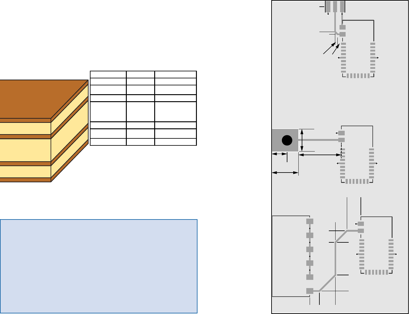
– – – –
100 101
Castellation Version Reference Design
The castellation connection for the antenna on the pre-certified version
allows the use of embedded antennas as well as removes the cost of
a cable assembly for the u.FL connector. However, the PCB design
and layer stack must follow one of the reference designs for the
certification on the HUM-900-PRO-CAS to be valid. Figure 108 shows
the PCB layer stack that should be used. Figure 109 shows the layout and
routing designs for the different antenna options. Please see the antenna
data sheets for specific ground plane counterpoise requirements.
Top Layer
Dielectric 1
Mid-Layer 1
Dielectric 2
Mid-Layer 2
Dielectric 3
Bottom Layer
Layer Name Thickness Material
1.4mil
1.4mil
1.4mil
1.4mil
14.00mil
14.00mil
28.00mil
Copper
Copper
Copper
Copper
FR-4 (Er = 4.6)
FR-4 (Er = 4.6)
FR-4 (Er = 4.6)
140
200
165
470
230
230 165
ANT-916-SP
ANT-916-PW-LP
ANT-916-PW-RA
ANT-916-CW-QW
ANT-916-CW-HW
ANT-916-WRT-RPS
Microstrip Width = 24mil
Ground plane on Mid-Layer 1
Units are in mils
619 361
72
35 35
CONREVSMA003.062
380
320
216
Figure 109: HumPROTM Series Transceiver Castellation Version Reference Design
Figure 108: HumPROTM Series Transceiver Castellation Version Reference Design PCB Stack
Note: The PCB design and layer stack for the HUM-900-RC-CAS must
follow these reference designs for the pre-certification to be valid.
The HUM-900-RC-UFL and the HUM-900-RC-CAS must use one of
the antennas in Figure 44 in order for the certification to be valid.
The HUM-900-RC and HUM-2.4-RC have not been tested and require
full compliance testing in the end product as it will go to market.
All modules require unintentional radiator compliance testing in the end
product as it will go to market.

– – – –
102 103
Power Supply Requirements
The module does not have an internal
voltage regulator, therefore it requires a clean,
well-regulated power source. The power supply
noise should be less than 20mV. Power supply
noise can significantly affect the module’s
performance, so providing a clean power supply
for the module should be a high priority during
design.
A 10Ω resistor in series with the supply followed by a 10µF tantalum
capacitor from Vcc to ground helps in cases where the quality of supply
power is poor (Figure 110). This filter should be placed close to the
module’s supply lines. These values may need to be adjusted depending
on the noise present on the supply line.
Antenna Considerations
The choice of antennas is a
critical and often overlooked
design consideration. The range,
performance and legality of an RF
link are critically dependent upon the
antenna. While adequate antenna
performance can often be obtained
by trial and error methods, antenna
design and matching is a complex
task. Professionally designed antennas such as those from Linx (Figure
111) help ensure maximum performance and FCC and other regulatory
compliance.
Linx transmitter modules typically have an output power that is higher
than the legal limits. This allows the designer to use an inefficient antenna
such as a loop trace or helical to meet size, cost or cosmetic requirements
and still achieve full legal output power for maximum range. If an efficient
antenna is used, then some attenuation of the output power will likely be
needed.
It is usually best to utilize a basic quarter-wave whip until your prototype
product is operating satisfactorily. Other antennas can then be evaluated
based on the cost, size and cosmetic requirements of the product.
Additional details are in Application Note AN-00500.
+
10Ω
10µF
Vcc IN
Vcc TO
MODULE
Figure 110: Supply Filter
Figure 111: Linx Antennas
Interference Considerations
The RF spectrum is crowded and the potential for conflict with unwanted
sources of RF is very real. While all RF products are at risk from
interference, its effects can be minimized by better understanding its
characteristics.
Interference may come from internal or external sources. The first step
is to eliminate interference from noise sources on the board. This means
paying careful attention to layout, grounding, filtering and bypassing in
order to eliminate all radiated and conducted interference paths. For
many products, this is straightforward; however, products containing
components such as switching power supplies, motors, crystals and other
potential sources of noise must be approached with care. Comparing your
own design with a Linx evaluation board can help to determine if and at
what level design-specific interference is present.
External interference can manifest itself in a variety of ways. Low-level
interference produces noise and hashing on the output and reduces the
link’s overall range.
High-level interference is caused by nearby products sharing the same
frequency or from near-band high-power devices. It can even come from
your own products if more than one transmitter is active in the same area.
It is important to remember that only one transmitter at a time can occupy
a frequency, regardless of the coding of the transmitted signal. This type of
interference is less common than those mentioned previously, but in severe
cases it can prevent all useful function of the affected device.
Although technically not interference, multipath is also a factor to be
understood. Multipath is a term used to refer to the signal cancellation
effects that occur when RF waves arrive at the receiver in different phase
relationships. This effect is a particularly significant factor in interior
environments where objects provide many different signal reflection paths.
Multipath cancellation results in lowered signal levels at the receiver and
shorter useful distances for the link.
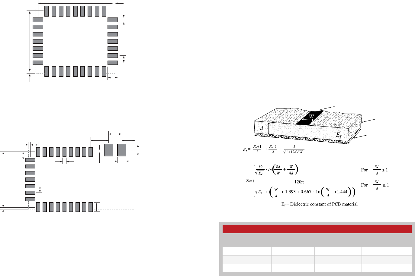
– – – –
104 105
Pad Layout
The pad layout diagrams below are designed to facilitate both hand and
automated assembly. Figure 112 shows the footprint for the smaller version
and Figure 113 shows the footprint for the pre-certified version.
0.420"
0.015"
0.028"
0.050"
0.060"
0.070"
0.015"
0.136"
0.100"
0.101"
0.060"
0.065"
0.090"
0.015"
0.420"
0.015"
0.028"
0.050"
0.520"
0.070"
0.015"
Figure 112: HUM-***-PRO Recommended PCB Layout
Figure 113: HUM-***-PRO-UFL/CAS Recommended PCB Layout
Microstrip Details
A transmission line is a medium whereby RF energy is transferred from
one place to another with minimal loss. This is a critical factor, especially in
high-frequency products like Linx RF modules, because the trace leading
to the module’s antenna can effectively contribute to the length of the
antenna, changing its resonant bandwidth. In order to minimize loss and
detuning, some form of transmission line between the antenna and the
module should be used unless the antenna can be placed very close (<1⁄8in)
to the module. One common form of transmission line is a coax cable and
another is the microstrip. This term refers to a PCB trace running over a
ground plane that is designed to serve as a transmission line between the
module and the antenna. The width is based on the desired characteristic
impedance of the line, the thickness of the PCB and the dielectric constant
of the board material. For standard 0.062in thick FR-4 board material, the
trace width would be 111 mils. The correct trace width can be calculated
for other widths and materials using the information in Figure 114 and
examples are provided in Figure 115. Software for calculating microstrip
lines is also available on the Linx website.
Trace
Board
Ground plane
Figure 114: Microstrip Formulas
Example Microstrip Calculations
Dielectric Constant Width / Height
Ratio (W / d)
Effective Dielectric
Constant
Characteristic
Impedance (Ω)
4.80 1.8 3.59 50.0
4.00 2.0 3.07 51.0
2.55 3.0 2.12 48.8
Figure 115: Example Microstrip Calculations

– – – –
106 107
Board Layout Guidelines
The module’s design makes integration straightforward; however, it
is still critical to exercise care in PCB layout. Failure to observe good
layout techniques can result in a significant degradation of the module’s
performance. A primary layout goal is to maintain a characteristic
50-ohm impedance throughout the path from the antenna to the module.
Grounding, filtering, decoupling, routing and PCB stack-up are also
important considerations for any RF design. The following section provides
some basic design guidelines.
During prototyping, the module should be soldered to a properly laid-out
circuit board. The use of prototyping or “perf” boards results in poor
performance and is strongly discouraged. Likewise, the use of sockets
can have a negative impact on the performance of the module and is
discouraged.
The module should, as much as reasonably possible, be isolated from
other components on your PCB, especially high-frequency circuitry such as
crystal oscillators, switching power supplies, and high-speed bus lines.
When possible, separate RF and digital circuits into different PCB regions.
Make sure internal wiring is routed away from the module and antenna and
is secured to prevent displacement.
Do not route PCB traces directly under the module. There should not be
any copper or traces under the module on the same layer as the module,
just bare PCB. The underside of the module has traces and vias that could
short or couple to traces on the product’s circuit board.
The Pad Layout section shows a typical PCB footprint for the module. A
ground plane (as large and uninterrupted as possible) should be placed on
a lower layer of your PC board opposite the module. This plane is essential
for creating a low impedance return for ground and consistent stripline
performance.
Use care in routing the RF trace between the module and the antenna
or connector. Keep the trace as short as possible. Do not pass it under
the module or any other component. Do not route the antenna trace on
multiple PCB layers as vias add inductance. Vias are acceptable for tying
together ground layers and component grounds and should be used in
multiples. The -CAS version must follow the layout in Figure 109.
Each of the module’s ground pins should have short traces tying
immediately to the ground plane through a via.
Bypass caps should be low ESR ceramic types and located directly
adjacent to the pin they are serving.
A 50-ohm coax should be used for connection to an external antenna.
A 50-ohm transmission line, such as a microstrip, stripline or coplanar
waveguide should be used for routing RF on the PCB. The Microstrip
Details section provides additional information.
In some instances, a designer may wish to encapsulate or “pot” the
product. There are a wide variety of potting compounds with varying
dielectric properties. Since such compounds can considerably impact
RF performance and the ability to rework or service the product, it is
the responsibility of the designer to evaluate and qualify the impact and
suitability of such materials.
Helpful Application Notes from Linx
It is not the intention of this manual to address in depth many of the issues
that should be considered to ensure that the modules function correctly
and deliver the maximum possible performance. We recommend reading
the application notes listed in Figure 116 which address in depth key areas
of RF design and application of Linx products. These applications notes
are available online at www.linxtechnologies.com or by contacting the Linx
literature department.
Helpful Application Note Titles
Note Number Note Title
AN-00100 RF 101: Information for the RF Challenged
AN-00126 Considerations for Operation Within the 902–928MHz Band
AN-00130 Modulation Techniques for Low-Cost RF Data Links
AN-00140 The FCC Road: Part 15 from Concept to Approval
AN-00500 Antennas: Design, Application, Performance
AN-00501 Understanding Antenna Specifications and Operation
Figure 116: Helpful Application Note Titles
– – – –
108 109
Production Guidelines
The module is housed in a hybrid SMD package that supports hand and
automated assembly techniques. Since the modules contain discrete
components internally, the assembly procedures are critical to ensuring
the reliable function of the modules. The following procedures should be
reviewed with and practiced by all assembly personnel.
Hand Assembly
Pads located on the bottom
of the module are the primary
mounting surface (Figure 117).
Since these pads are inaccessible
during mounting, castellations
that run up the side of the module
have been provided to facilitate
solder wicking to the module’s
underside. This allows for very
quick hand soldering for prototyping and small volume production. If the
recommended pad guidelines have been followed, the pads will protrude
slightly past the edge of the module. Use a fine soldering tip to heat the
board pad and the castellation, then introduce solder to the pad at the
module’s edge. The solder will wick underneath the module, providing
reliable attachment. Tack one module corner first and then work around the
device, taking care not to exceed the times in Figure 118.
Automated Assembly
For high-volume assembly, the modules are generally auto-placed.
The modules have been designed to maintain compatibility with reflow
processing techniques; however, due to their hybrid nature, certain aspects
of the assembly process are far more critical than for other component
types. Following are brief discussions of the three primary areas where
caution must be observed.
Castellations
PCB Pads
Soldering Iron
Tip
Solder
Figure 117: Soldering Technique
Warning: Pay attention to the absolute maximum solder times.
Figure 118: Absolute Maximum Solder Times
Absolute Maximum Solder Times
Hand Solder Temperature: +427ºC for 10 seconds for lead-free alloys
Reflow Oven: +255ºC max (see Figure 119)
Reflow Temperature Profile
The single most critical stage in the automated assembly process is the
reflow stage. The reflow profile in Figure 119 should not be exceeded
because excessive temperatures or transport times during reflow will
irreparably damage the modules. Assembly personnel need to pay careful
attention to the oven’s profile to ensure that it meets the requirements
necessary to successfully reflow all components while still remaining
within the limits mandated by the modules. The figure below shows the
recommended reflow oven profile for the modules.
Shock During Reflow Transport
Since some internal module components may reflow along with the
components placed on the board being assembled, it is imperative that
the modules not be subjected to shock or vibration during the time solder
is liquid. Should a shock be applied, some internal components could be
lifted from their pads, causing the module to not function properly.
Washability
The modules are wash-resistant, but are not hermetically sealed. Linx
recommends wash-free manufacturing; however, the modules can be
subjected to a wash cycle provided that a drying time is allowed prior
to applying electrical power to the modules. The drying time should be
sufficient to allow any moisture that may have migrated into the module
to evaporate, thus eliminating the potential for shorting damage during
power-up or testing. If the wash contains contaminants, the performance
may be adversely affected, even after drying.
125°C
185°C
217°C
255°C
235°C
60 12030 150180 210240 270300 330360090
50
100
150
200
250
300
Recommended RoHS Profile
Max RoHS Profile
Recommended Non-RoHS Profile
180°C
Temperature (oC)
Time (Seconds)
Figure 119: Maximum Reflow Temperature Profile
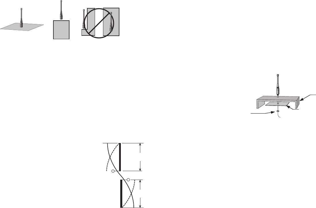
– – – –
110 111
General Antenna Rules
The following general rules should help in maximizing antenna performance.
1. Proximity to objects such as a user’s hand, body or metal objects will
cause an antenna to detune. For this reason, the antenna shaft and tip
should be positioned as far away from such objects as possible.
2. Optimum performance is obtained from a ¼- or ½-wave straight whip
mounted at a right angle to the ground plane (Figure 120). In many
cases, this isn’t desirable for practical or ergonomic reasons, thus,
an alternative antenna style such as a helical, loop or patch may be
utilized and the corresponding sacrifice in performance accepted.
3. If an internal antenna is to be used, keep it away from other metal
components, particularly large items like transformers, batteries,
PCB tracks and ground planes. In many cases, the space around the
antenna is as important as the antenna itself. Objects in close proximity
to the antenna can cause direct detuning, while those farther away will
alter the antenna’s symmetry.
4. In many antenna designs, particularly ¼-wave whips, the ground plane
acts as a counterpoise, forming, in essence,
a ½-wave dipole (Figure 121). For this reason,
adequate ground plane area is essential.
The ground plane can be a metal case or
ground-fill areas on a circuit board. Ideally, it
should have a surface area less than or equal
to the overall length of the ¼-wave radiating
element. This is often not practical due to
size and configuration constraints. In these
instances, a designer must make the best use
of the area available to create as much ground
OPTIMUM
USABLE NOT RECOMMENDED
NUT GROUND PLANE
(MAY BE NEEDED)
CASE
Figure 120: Ground Plane Orientation
I
EDIPOLE
ELEMENT
GROUND
PLANE
VIRTUAL λ/4
DIPOLE
λ/4
λ/4
VERTICAL λ/4 GROUNDED
ANTENNA (MARCONI)
Figure 121: Dipole Antenna
plane as possible in proximity to the base of the antenna. In cases
where the antenna is remotely located or the antenna is not in close
proximity to a circuit board, ground plane or grounded metal case, a
metal plate may be used to maximize the antenna’s performance.
5. Remove the antenna as far as possible from potential interference
sources. Any frequency of sufficient amplitude to enter the receiver’s
front end will reduce system range and can even prevent reception
entirely. Switching power supplies, oscillators or even relays can also
be significant sources of potential interference. The single best weapon
against such problems is attention to placement and layout. Filter the
module’s power supply with a high-frequency bypass capacitor. Place
adequate ground plane under potential sources of noise to shunt noise
to ground and prevent it from coupling to the RF stage. Shield noisy
board areas whenever practical.
6. In some applications, it is advantageous to place the module and
antenna away from the main equipment (Figure 122). This can avoid
interference problems and allows the antenna to be oriented for
optimum performance. Always use 50Ω coax, like RG-174, for the
remote feed.
OPTIMUM
USABLE NOT RECOMMENDED
NUT GROUND PLANE
(MAY BE NEEDED)
CASE
Figure 122: Remote Ground Plane
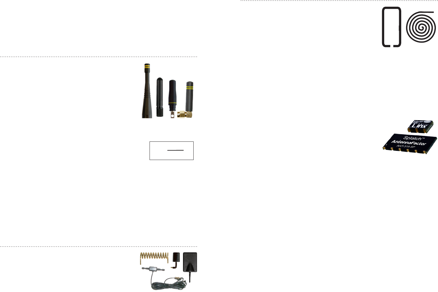
– – – –
112 113
Common Antenna Styles
There are hundreds of antenna styles and variations that can be employed
with Linx RF modules. Following is a brief discussion of the styles most
commonly utilized. Additional antenna information can be found in Linx
Application Notes AN-00100, AN-00140, AN-00500 and AN-00501. Linx
antennas and connectors offer outstanding performance at a low price.
Whip Style
A whip style antenna (Figure 123) provides
outstanding overall performance and stability.
A low-cost whip can be easily fabricated from
a wire or rod, but most designers opt for the
consistent performance and cosmetic appeal of
a professionally-made model. To meet this need,
Linx offers a wide variety of straight and reduced
height whip style antennas in permanent and
connectorized mounting styles.
The wavelength of the operational frequency determines
an antenna’s overall length. Since a full wavelength
is often quite long, a partial ½- or ¼-wave antenna
is normally employed. Its size and natural radiation
resistance make it well matched to Linx modules.
The proper length for a straight ¼-wave can be easily
determined using the formula in Figure 124. It is also
possible to reduce the overall height of the antenna by
using a helical winding. This reduces the antenna’s bandwidth but is a great
way to minimize the antenna’s physical size for compact applications. This
also means that the physical appearance is not always an indicator of the
antenna’s frequency.
Specialty Styles
Linx offers a wide variety of specialized antenna
styles (Figure 125). Many of these styles utilize
helical elements to reduce the overall antenna size
while maintaining reasonable performance. A helical
antenna’s bandwidth is often quite narrow and the
antenna can detune in proximity to other objects, so
care must be exercised in layout and placement.
L =
234
F
MHz
Figure 123: Whip Style Antennas
Figure 124:
L = length in feet of
quarter-wave length
F = operating frequency
in megahertz
Figure 125: Specialty Style
Antennas
Loop Style
A loop or trace style antenna is normally printed
directly on a product’s PCB (Figure 126). This
makes it the most cost-effective of antenna
styles. The element can be made self-resonant or
externally resonated with discrete components,
but its actual layout is usually product specific.
Despite the cost advantages, loop style antennas
are generally inefficient and useful only for short
range applications. They are also very sensitive to changes in layout and
PCB dielectric, which can cause consistency issues during production.
In addition, printed styles are difficult to engineer, requiring the use of
expensive equipment including a network analyzer. An improperly designed
loop will have a high VSWR at the desired frequency which can cause
instability in the RF stage.
Linx offers low-cost planar (Figure 127) and chip
antennas that mount directly to a product’s PCB.
These tiny antennas do not require testing and
provide excellent performance despite their small
size. They offer a preferable alternative to the often
problematic “printed” antenna.
Figure 126: Loop or Trace Antenna
Figure 127: SP Series
“Splatch” and uSP
“MicroSplatch” Antennas

– – – –
114 115
Regulatory Considerations
When working with RF, a clear distinction must be made between what
is technically possible and what is legally acceptable in the country where
operation is intended. Many manufacturers have avoided incorporating RF
into their products as a result of uncertainty and even fear of the approval
and certification process. Here at Linx, our desire is not only to expedite the
design process, but also to assist you in achieving a clear idea of what is
involved in obtaining the necessary approvals to legally market a completed
product.
For information about regulatory approval, read AN-00142 on the Linx
website or call Linx. Linx designs products with worldwide regulatory
approval in mind.
In the United States, the approval process is actually quite straightforward.
The regulations governing RF devices and the enforcement of them are
the responsibility of the Federal Communications Commission (FCC). The
regulations are contained in Title 47 of the United States Code of Federal
Regulations (CFR). Title 47 is made up of numerous volumes; however,
all regulations applicable to this module are contained in Volume 0-19.
It is strongly recommended that a copy be obtained from the FCC’s
website, the Government Printing Office in Washington or from your local
government bookstore. Excerpts of applicable sections are included
with Linx evaluation kits or may be obtained from the Linx Technologies
website, www.linxtechnologies.com. In brief, these rules require that any
device that intentionally radiates RF energy be approved, that is, tested for
compliance and issued a unique identification number. This is a relatively
painless process. Final compliance testing is performed by one of the many
independent testing laboratories across the country. Many labs can also
provide other certifications that the product may require at the same time,
such as UL, CLASS A / B, etc. Once the completed product has passed,
an ID number is issued that is to be clearly placed on each product
manufactured.
Note: Linx RF modules are designed as component devices that require
external components to function. The purchaser understands that
additional approvals may be required prior to the sale or operation of
the device, and agrees to utilize the component in keeping with all laws
governing its use in the country of operation.
Questions regarding interpretations of the Part 2 and Part 15 rules or the
measurement procedures used to test intentional radiators such as Linx RF
modules for compliance with the technical standards of Part 15 should be
addressed to:
Federal Communications Commission
Equipment Authorization Division
Customer Service Branch, MS 1300F2
7435 Oakland Mills Road
Columbia, MD, US 21046
Phone: + 1 301 725 585 | Fax: + 1 301 344 2050
Email: labinfo@fcc.gov
ETSI Secretaria
650, Route des Lucioles
06921 Sophia-Antipolis Cedex
FRANCE
Phone: +33 (0)4 92 94 42 00
Fax: +33 (0)4 93 65 47 16
International approvals are slightly more complex, although Linx modules
are designed to allow all international standards to be met. If the end
product is to be exported to other countries, contact Linx to determine the
specific suitability of the module to the application.
All Linx modules are designed with the approval process in mind and thus
much of the frustration that is typically experienced with a discrete design is
eliminated. Approval is still dependent on many factors, such as the choice
of antennas, correct use of the frequency selected and physical packaging.
While some extra cost and design effort are required to address these
issues, the additional usefulness and profitability added to a product by RF
makes the effort more than worthwhile.

Disclaimer
Linx Technologies is continually striving to improve the quality and function of its products. For this reason, we
reserve the right to make changes to our products without notice. The information contained in this Data Guide
is believed to be accurate as of the time of publication. Specifications are based on representative lot samples.
Values may vary from lot-to-lot and are not guaranteed. “Typical” parameters can and do vary over lots and
application. Linx Technologies makes no guarantee, warranty, or representation regarding the suitability of any
product for use in any specific application. It is the customer’s responsibility to verify the suitability of the part for
the intended application. NO LINX PRODUCT IS INTENDED FOR USE IN ANY APPLICATION WHERE THE SAFETY
OF LIFE OR PROPERTY IS AT RISK.
Linx Technologies DISCLAIMS ALL WARRANTIES OF MERCHANTABILITY AND FITNESS FOR A PARTICULAR
PURPOSE. IN NO EVENT SHALL LINX TECHNOLOGIES BE LIABLE FOR ANY OF CUSTOMER’S INCIDENTAL OR
CONSEQUENTIAL DAMAGES ARISING IN ANY WAY FROM ANY DEFECTIVE OR NON-CONFORMING PRODUCTS
OR FOR ANY OTHER BREACH OF CONTRACT BY LINX TECHNOLOGIES. The limitations on Linx Technologies’
liability are applicable to any and all claims or theories of recovery asserted by Customer, including, without
limitation, breach of contract, breach of warranty, strict liability, or negligence. Customer assumes all liability
(including, without limitation, liability for injury to person or property, economic loss, or business interruption) for
all claims, including claims from third parties, arising from the use of the Products. The Customer will indemnify,
defend, protect, and hold harmless Linx Technologies and its officers, employees, subsidiaries, affiliates,
distributors, and representatives from and against all claims, damages, actions, suits, proceedings, demands,
assessments, adjustments, costs, and expenses incurred by Linx Technologies as a result of or arising from any
Products sold by Linx Technologies to Customer. Under no conditions will Linx Technologies be responsible for
losses arising from the use or failure of the device in any application, other than the repair, replacement, or refund
limited to the original product purchase price. Devices described in this publication may contain proprietary,
patented, or copyrighted techniques, components, or materials. Under no circumstances shall any user be
conveyed any license or right to the use or ownership of such items.
©2015 Linx Technologies. All rights reserved.
The stylized Linx logo, Wireless Made Simple, WiSE, CipherLinx and the stylized CL logo are trademarks of Linx Technologies.
Linx Technologies
159 Ort Lane
Merlin, OR, US 97532
Phone: +1 541 471 6256
Fax: +1 541 471 6251
www.linxtechnologies.com