Logitech Canada LZM2102 RADIO-Z MODULE User Manual RADIO 2 Z
Logitech Inc.- Canada RADIO-Z MODULE RADIO 2 Z
USERS MANUAL

Radio Z DataSheet
Author : Samuel Asare & Khalid Mehmood
Logitech Inc-Canada

L-ZM2102
Preliminary Datasheet
Datasheet
L-ZM2102 Z-Wave Module Datasheet
This document is the property of Logitech Inc-Canada. The data contained herein, in
whole or in part, may not be duplicated, used or disclosed outside the recipient for any
purpose other than to conduct technical evaluation. This restriction does not limit the
recipient's right to use information contained in the data if it is obtained from another
source without restriction.
REVISION RECORD
Doc. Rev Date By Pages affected Brief description of changes
01.00 20050412 TJO ALL First release
01.01 20050718 TJO Table 4: SAW filter insertion note inserted
Table 5: Min temp extended from -15¡C to -30¡C
Table 6: footnote 2 added
Chapter 2.7 inserted: Reflow profile
Table 7: module weight inserted
Chapter 3.1: wording changed
L-ZM2102
Preliminary Datasheet
Integrated Z-Wave RF Module
The L-ZM2102 Z-Wave Module is a fully integrated RF communication module that uses the
unlicensed Short-Range-Device (SRD) frequency band of 868.42MHz in Europe and 908.42MHz
in US. The L-ZM2102 is dedicated for wireless control and monitoring of residential products like
lighting and appliance control, energy management, access control, security and building
automation.
Together with the patented Z-Wave Protocol the L-ZM2102 Z-Wave Module delivers a complete
highly reliable RF communication solution. The Z-Wave Protocol uses Frame Acknowledgement,
Retransmission, Collision Avoidance, Frame Checksum Check and sophisticated Routing to
assure reliable full home coverage.
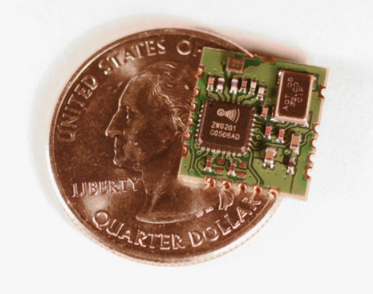
The L-ZM2102 Z-Wave Module contains the integrated ZW0201 Z-Wave Single Chip, system
crystal and RF front-end circuitry. The ZW0201 Single Chip is an integrated chip containing RF
Transceiver, 8051 MCU core, SRAM, Flash Memory for Z-Wave Protocol and OEM Application
software storage, Triac Controller and a wide range of HW interfaces.
This complete RF solution makes it very easy for OEM customers to RF enable their products
without having to do the time consuming work of designing, verifying and optimizing the RF
design and thereby enables faster time to marked.
Features
APPENDIX A.1 Interfaces
• 10 General Purpose I/O’s
• Two Interrupt Inputs
• Serial UART
• SPI Interface
• Triac Control Interface
• PWM Output
• Four multiplexed 12/8 bit ADC inputs
APPENDIX A.2
APPENDIX A.3 ZW0201 Single Chip
• Optimized 8051 CPU Core
• 32kbyte Flash
• 2kbyte SRAM
• Power-On-Reset / Brown-Out Detection
• Supply Voltage: 2.1V-3.6V
• Power Consumption
o TX@-5dBm = 23mA
o TX@+3dBm = 39mA
o RX = 21mA
o Power down/sleep mode = 2.5µA
APPENDIX A.4 RF
• Freq: 908.42MHz (US) / 868.42MHz (EU)
• High Sensitivity (-101dBm)
• FSK Modulation
• 9.6kbit/s Data Rate
• -20dBm to +3dBm Output power (ZW0201)
• Complies with EN 300 220 and FCC CFR47 part 15
APPENDIX A.5 Applications
• Home Automation
o Lighting/Drape Control
o Automated Meter Reading
o Access Control
o HVAC
o Universal Remote Controls

MPQ Test Radio Z
2005-10-03
LOGITECH CONFIDENTIAL
(Printed on 10/3/2005 ) page 6 of 19
Table of Contents
Compliance Statement
1 PRODUCT DESCRIPTION...................................................................................................................5
1.1 Overview................................................................................................................................................5
1.2 Signal Description..................................................................................................................................6
1.3 RF Front-End.........................................................................................................................................7
1.3.1 RF input/output...........................................................................................................................7
1.3.2 Antenna Matching.......................................................................................................................7
1.4 Z-Wave Module Programming..............................................................................................................8
2 SPECIFICATIONS................................................................................................................................9
2.1 ZW0201 Specification...........................................................................................................................9
2.2 ZW0201 Single Chip Peripherals..........................................................................................................9
2.3 RF Specification....................................................................................................................................9
2.4 Electrical Specification........................................................................................................................10
2.4.1 Absolute Maximum Ratings......................................................................................................10
2.4.2 DC Characteristics....................................................................................................................10
2.5 Physical Specification..........................................................................................................................11
2.6 Process Specification..........................................................................................................................11
2.7 Recommended PCB Footprint Outline................................................................................................12
2.8 Recommended Reflow Profile.............................................................................................................13
2.9 Application PCB Layout Recommendation.........................................................................................13
2.9.1 Supply Voltage.........................................................................................................................13
2.9.2 Ground Plane...........................................................................................................................14
2.9.3 Antenna Interconnection...........................................................................................................14
3 SOFTWARE........................................................................................................................................15
3.1 SPI Interface........................................................................................................................................15
3.2 EEPROM.............................................................................................................................................15
4 REFERENCE......................................................................................................................................16

MPQ Test Radio Z
2005-10-03
LOGITECH CONFIDENTIAL
(Printed on 10/3/2005 ) page 7 of 19
Compliance Statement
FCC Class B Part 15
This device complies with part 15 of the FCC Rules. Operation is subject to the following two conditions: (1) This
device may not cause harmful interference, and (2) this device must accept any interference received, including
interference that may cause undesired operation.
Warning: Changes or modifications not expressly approved by the party responsible for compliance could void
the user’s authority to operate the equipment.
NOTE: This equipment has been tested and found to comply with the limits for a Class B digital device, pursuant
to part 15 of the FCC Rules. These limits are designed to provide reasonable protection against harmful
interference in a residential installation. This equipment generates, uses and can radiate radio frequency energy
and, if not installed and used in accordance with the instructions, may cause harmful interference to radio
communications. However, there is no guarantee that interference will not occur in a particular installation. If this
equipment does cause harmful interference to radio or television reception, which can be determined by turning the
equipment off and on, the user is encouraged to try to correct the interference by one or more of the following
measures:
- Reorient or relocate the receiving antenna.
- Increase the separation between the equipment and receiver.
- Connect the equipment into an outlet on a circuit different from that to which the receiver is connected.
- Consult the dealer or an experienced radio/TV technician for help.
If the FCC ID for the module is not visible when the module is installed inside another device, then the outside of
the device into which the module is installed must display a label referring to the enclosed module. This exterior
label can use wording such as the following:
Contains FCC ID: TOB-LZM2102
MPQ Test Radio Z
2005-10-03
LOGITECH CONFIDENTIAL
(Printed on 10/3/2005 ) page 8 of 19
1 PRODUCT DESCRIPTION
1.1 Overview
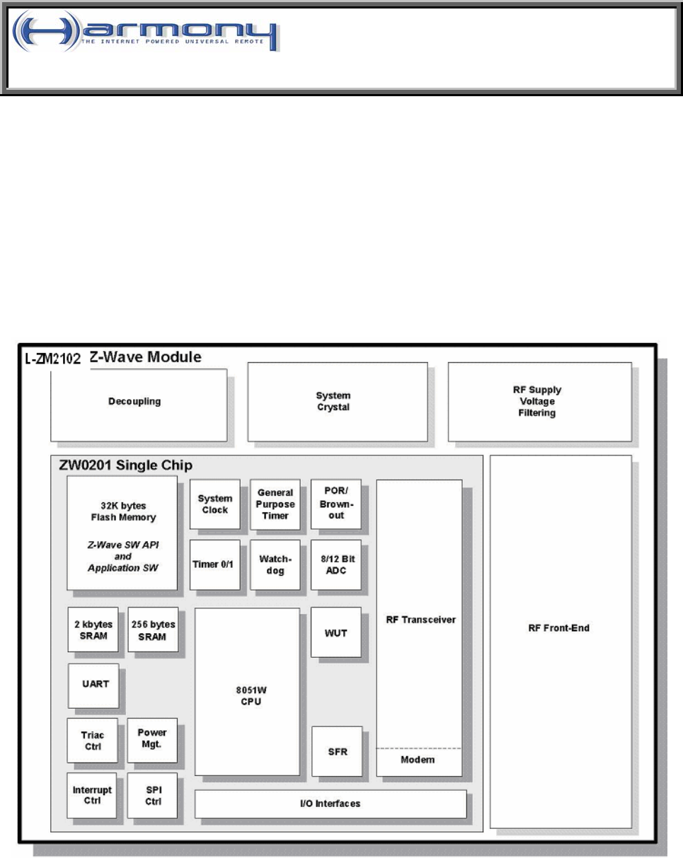
The L-ZM2102 Z-Wave Module is a fully integrated module containing all the HW and SW required to Z-
Wave enable OEM products. The L-ZM2102 Z-Wave Module contains the Z-Wave ZW0201 Single Chip,
System Crystal, RF Front-end and RF Supply Voltage Filtering. Only the antenna needs to be
implemented by the developer designing the Z-Wave enabled product.
Figure 1 ZM2102 Z-Wave Module Block Diagram
The L-ZM2102 Z-Wave Module contains a system crystal, why no external crystal is needed. In order to
get a high reliable and high performance RF communication, the RF Front-end has an optimized and
throughout tested matching circuitry, a narrow band SAW filter dedicated for Z-Wave communication
and there are filtering of the RF circuitry supply voltage. The L-ZM2102 Z-Wave Module is connector-
MPQ Test Radio Z
2005-10-03
LOGITECH CONFIDENTIAL
(Printed on 10/3/2005 ) page 9 of 19
less using Castellation Notches for easy mounting of the module to an OEM Application PCB.
The L-ZM2102 Z-Wave Module has a top shield that improves noise immunity of the module and
enables the module to be mounted by a standard pick-and-place machine on the production line.
The Z-Wave Protocol is designed to enable automatic network address assignment at installation, and
simple inclusion/exclusion of nodes. These protocol-handling techniques ensure easy installation,
expansion, and management of the Z-Wave control network. Furthermore each Z-Wave network has its
own unique Network Identifier preventing control problems or interference from neighboring networks.
The Z-Wave Protocol has a well-defined Application-Programming-Interface (API) enabling easy and fast
Application SW development.
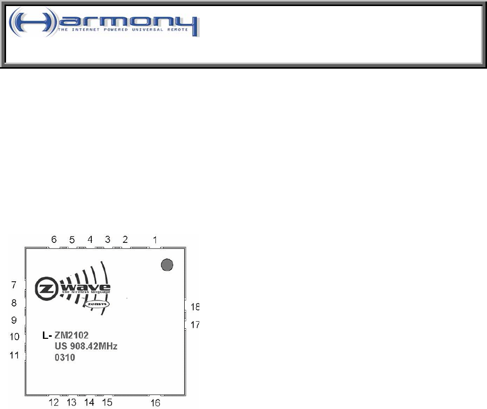
1.2 Signal Description
Notch
#
Signal
Name
1 GND
2 RESET_N
3 P1.7 /
INT1
4 P1.6 /
PWM /
INT0
5 P1.5
6 GND
7 P1.2 /
MISO1
8 P1.4 /
SCK1
9 P1.3 /
MOSI1
10 P1.1 /
ADC3 /
RXD
11 VCC
12 GND
13 P0.1 /

MPQ Test Radio Z
2005-10-03
LOGITECH CONFIDENTIAL
(Printed on 10/3/2005 ) page 10 of 19
ADC1 /
TRIAC
14 P0.0 /
ADC0 /
ZEROX
15 P1.0 /
ADC2 /
TXD
16 GND
17 GND
18 RF in/out
Figure 2 L-ZM2102 Outline and Signals
Name Notch # I/O Description
ADC[3:0] 10, 13, 14,
15
I Analog-to-Digital Converter input. The ADC is 12/8 bit and can use either
VCC or an internal/external voltage as reference.
ADC3: input
ADC2: input
ADC1: input / lower reference
ADC0: input / higher reference
GND 1, 6, 12, 16, 17 Power Ground signal
INT[1:0] 3, 4 I/O Interrupt: The signal can be either level or edge trigged. When in power
down mode, the L-ZM2102 Z-Wave Module’s MCU can be woken up by
asserting the interrupt signal.
P[0.1-
0.0],
P[1.7-1.0]
3, 4, 5, 7, 8, 9,
10, 13, 14, 15
I/O In/Out: General purpose I/O signal.
MISO1
7 I/O Master-In-Slave-Out SPI interface: output in slave mode operation and
input in master mode operation.
MOSI1
9 I/O Master Out Slave In SPI interface: input in slave mode operation and
output in master mode operation.
PWM 4 I/O Pulse Width Modulator Output: Used for frequency variation applications.
RESET_N 2 I Reset: Active low reset. The ZW0201 Single Chip has an integrated
Power-On-Reset and Brown-out detection circuitry.
RF 18 I/O RF Input/Output
RXD 10 I/O UART Receive Data: Supports 9.6kbaud, 38.4kbaud, 115.2kbaud.
SCK
1
8 I/O SPI Clock: Can be used as either master SPI clock output or slave SPI
clock input.
TRIAC 13 I/O TRIAC Control: A triac controller is implemented in the ZW0201
Single Chip that can controls a triac on the Application Module like
light dimmer modules etc.
MPQ Test Radio Z
2005-10-03
LOGITECH CONFIDENTIAL
(Printed on 10/3/2005 ) page 11 of 19
TXD 15 I/O UART Transmit Data: Supports 9.6kbaud, 38.4kbaud, 115.2kbaud.
VCC 11 Power L-ZM2102 supply voltage.
ZEROX 14 I/O Zero Cross Detection: Zero cross detection signal used on dimmer
modules detecting 120/240V zero crossing.
1. Please note that the SPI interface (MISO, MOSI and SCK) is not available for the Application SW in some Z-Wave protocol
API’s, see [3].
Table 1 L-ZM2102 Signal Description
All signals in Table 1 except RF, VCC and GND are connected directly to the corresponding signals on the
ZW0201 Z-Wave Single Chip on the L-ZM2102 Z-Wave Module. A detailed description of these signals is given
in the ZW0201 Z-Wave Single Chip datasheet [1].
1.3 RF Front-End
1.3.1 RF input/output
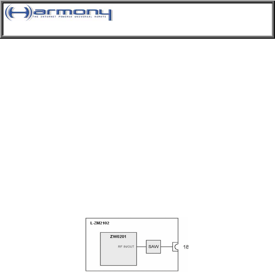
The L-ZM2102 Z-Wave Module is equipped with a SAW filter that rejects the unwanted frequencies both
in receive and transmit operations.
Figure 3 L-ZM2102 RF Front-end Circuitry
The RF input/output on the ZW0201 is a single ended input/output that is internally matched to 50 ohm.
1.3.2 Antenna Matching
The L-ZM2102 Z-Wave Module is using an antenna placed on the Application Module, the matching of
the external antenna to 50 ohm (SAW filter impedance) must be made on the Application Module.
As the L-ZM2102 Z-Wave Module is integrated into various products, different types of antennas can be
implemented to get the best RF performance, i.e. range and reliability. In [4], a good overview of the different
antennas is given as well as their pro’s and con’s. In the case the antenna is not 50ohm a matching network must be
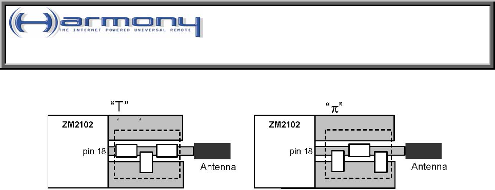
implemented between the L-ZM2102 Z-Wave Module and the antenna. The matching network can for example be
a “pi” or a “T” structure as shown in Figure 4.
MPQ Test Radio Z
2005-10-03
LOGITECH CONFIDENTIAL
(Printed on 10/3/2005 ) page 12 of 19
Figure 4 “π” ant “T” structure for the antenna-matching network
1.4 Z-Wave Module Programming
The L-ZM2102 Z-Wave Module is programmed using the SPI interface and the RESET_N signal. For detailed
programming instructions see [2] and recommended programming tool(s) see [3].
2 SPECIFICATIONS
2.1 ZW0201 Specification
MCU Description
MCU Type Optimized 8-bit 8051 MCU core.
MCU speed 16 MHz (integrated clock divider, external crystal frequency is 32MHz)
Flash 32kbyte. Programmed through the SPI interface.
SRAM 2kbyte
SRAM (CPU) 256byte
MCU
Peripherals
12/8-bit ADC, UART, SPI, 2x16 bit timers one with PWM mode, Watch Dog Timer,
Wake Up Timer, Power-on Reset/Brown-Out Detector.
Interrupt
sources
Internal and external.
Table 2 MCU Specifications
2.2 ZW0201 Single Chip Peripherals
Peripherals Description
Crystals System Clock: 32MHz, ±10ppm@25¡C, ±14ppm@-15¡C to +85¡C, 3ppm aging
per 5 years.
Alternative: 32MHz, ±8ppm@25¡C, ±8ppm@-15¡C to +85¡C, 3ppm aging per year.
Optional
Peripherals
EEPROM
Table 3 External Peripherals

MPQ Test Radio Z
2005-10-03
LOGITECH CONFIDENTIAL
(Printed on 10/3/2005 ) page 13 of 19
2.3 RF Specification
RF Description
RF Data rate 9.6 kbps
RF frequency (center frequency) US: 908.42 MHz
EU: 868.42 MHz
Modulation Frequency Shift Keying (FSK)
Frequency deviation Center frequency ± 25kHz
Signal coding Manchester Encoded
RF filter SAW Filter
US: Center frequency = 908MHz, BW = 20MHz
EU: Center frequency = 868MHz, BW = 20MHz
Typical RF receiver sensitivity -101dBm (including SAW filter)
ZW0201 RF Output Power (RF transceiver
output)
-20dBm to
+3dBm
Typical Saw filter insertion loss:
2.2dB
RF Input/Output Impedance 50ohm @ respective EU/US frequencies
Range (typical) Indoor >30 meters line of sight, in unobstructed
environment.
Outdoor > 60 meters line of sight
RF regulatory US: FCC Part 15
EU: R&TTE Directive 1999/5/EC, EN 300 220-3/2000
Table 4 RF Specifications
2.4 Electrical Specification
The “Absolute Maximum Ratings” specifies the conditions in which the L-ZM2102 Z-Wave Module is
guaranteed not to be damaged but correct operations are not guaranteed. Exceeding the “Absolute
Maximum Ratings” may destroy the L-ZM2102 Z-Wave Module. See “DC Characteristics” for
guaranteed operation limits.
2.4.1 Absolute Maximum Ratings
Electrical Value
Operating Temperature -30¡C to +85¡C
Storage Temperature -40¡C to +85¡C
Voltage on input pins -0.3V to VCC+0.3V (5V max)
Minimum Operating Voltage (VCC) -0.3V
Maximum Operating Voltage (VCC) 5V

MPQ Test Radio Z
2005-10-03
LOGITECH CONFIDENTIAL
(Printed on 10/3/2005 ) page 14 of 19
Table 5 Absolute Maximum Ratings
2.4.2 DC Characteristics
The following DC characteristics are preliminary for the L-ZM2102 Z-Wave Module.
TA = 25¡C, VCC = 3.3V (unless otherwise noted)
Symbol Parameter Condition Min Typ Max Units
VCC Digital Supply Voltage 2.1 3.3 3.6 V
RRST2
Reset Pull-up Resistor Integrated in ZW0201 10 MΩ
IC
Continuous Output Current One GPIO -20
20
mA
ICTOT
Total continuous output source/sink
current
All GPIO’s -
100
100
mA
ICC
Transmitting
(16MHz system clock)
-5dBm (transceiver
output)
+3dBm (transceiver
output)
23
39
mA
Receiving
(16MHz system clock)
VCC = 3.3V 21 mA
Power Down WUT active (POR enabled
1
) 2.5 µA
WUT disabled (POR enabled
1
) 2.5 µA
TOP Operating Temperature -15 85 ¡C
HOP Operating Relative Humidity 8 80 %
1. The POR cannot be disabled
2. The integrated Reset pull up is not for external circuitry. An external pull up resistor should be implemented.
Table 6 DC Characteristics
2.5 Physical Specification
Physical Specification Description
Size 12.5mm. x 13.6mm. x 2.4mm (0.492” x 0.535” x 0.094”)
Weight 7g (with shield)

MPQ Test Radio Z
2005-10-03
LOGITECH CONFIDENTIAL
(Printed on 10/3/2005 ) page 15 of 19
5g (without shield)
Castellation Notches 18
Table 7 Physical Specifications
2.6 Process Specification
Specification Description
MSL-3 Moisture Level Verification tested according to JEDEC J-STD-020C
RoHS Designed in compliance with The Restriction of Hazardous Substances Directive (RoHS)
Table 8 Process Specifications
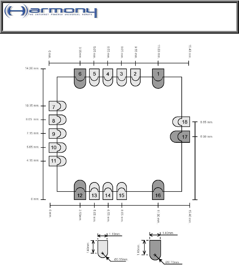
2.7 Recommended PCB Footprint Outline
MPQ Test Radio Z
2005-10-03
LOGITECH CONFIDENTIAL
(Printed on 10/3/2005 ) page 16 of 19
Figure 5 Recommend L-ZM2102 PCB footprint Outline
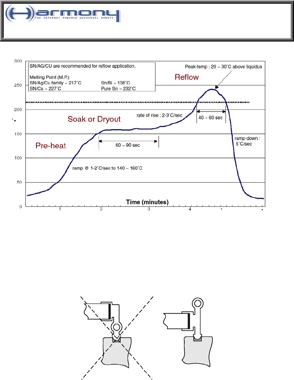
2.8 Recommended Reflow Profile
MPQ Test Radio Z
2005-10-03
LOGITECH CONFIDENTIAL
(Printed on 10/3/2005 ) page 17 of 19
Figure 6 Recommended Reflow Temperature Profile
2.9 Application PCB Layout Recommendation
2.9.1 Supply Voltage
As the L-ZM2102 Z-Wave Module contains a RF transceiver good supply voltage decoupling is important. Two
decoupling capacitors should be placed at the VCC pin (EP11) a 4.7uF and a 100nF capacitor is recommended.
The two capacitors should be placed as close EP11 as possible and the capacitor should be placed between the L-
ZM2102 Z-Wave Module and the via that goes to the power plane as shown in Figure 7.
Figure 7 Placement of decoupling capacitor (power pin, EP11)
2.9.2 Ground Plane
In order to minimize any noise coupling from noisy signals (typically power products) it is recommended
MPQ Test Radio Z
2005-10-03
LOGITECH CONFIDENTIAL
(Printed on 10/3/2005 ) page 18 of 19
to insert as much ground cobber below the L-ZM2102 Z-Wave Module as possible on the Application
PCB.
2.9.3 Antenna Interconnection
As the RF signal (EP18) is 50ohm the trace from the EP18 to the matching circuitry (see 1.3.2) must be 50ohm.
The Application PCB designer must therefore take the PCB layer structure and thickness into account when
designing the 50ohm trace (either Microstrip or Stripline).
3 SOFTWARE
3.1 SPI Interface
The signals ‘P1.2/MISO’, ‘P1.4/SCK’ and ‘P1.3/MOSI’ signals are in some SW API’s used by the protocol to
store Routing Tables and HomeID in an external EEPROM. When these SW API’s are used, the Application SW
must not use these three signals. Table 9 shows the available SW API’s and in which the SPI interface is used by
the protocol.
SW API SPI interface used by Protocol
Slave No
Routing Slave No
Enhanced Slave Yes
Controller Yes
Static Controller Yes
Installer Yes
Bridge Yes
Table 9 SW API / SPI availability
3.2 EEPROM
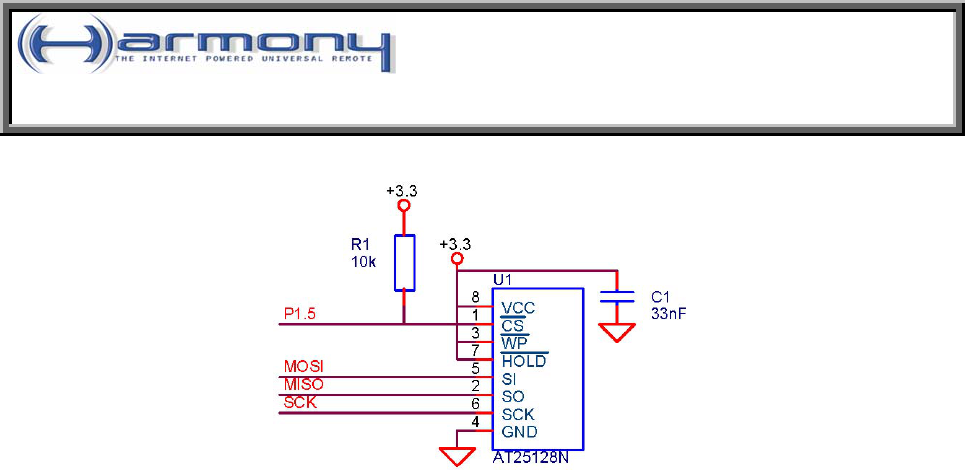
Some SW API’s require an external EEPROM to be implemented on the Application PCB for protocol information
storage (like routing table, HomeID etc.). The SPI interface is used to access the EEPROM and the ‘P1.5’ signal
(EP5) is used by the Z-Wave Protocol as EEPROM Chip Select. To assure proper control of the EEPROM chip
select signal during reset and power-up a pull up resistor on the P1.5 should be implemented as shown in Figure 8.
MPQ Test Radio Z
2005-10-03
LOGITECH CONFIDENTIAL
(Printed on 10/3/2005 ) page 19 of 19
Figure 8 External EEPROM
Only a part of the EEPROM is used for protocol data storage, the Application SW can use the remaining memory
area using an API call (see [3]). For the EEPROM memory area requirements of the protocol API please refer to
the documentation for the Z-Wave Controller code selected (see [3]).