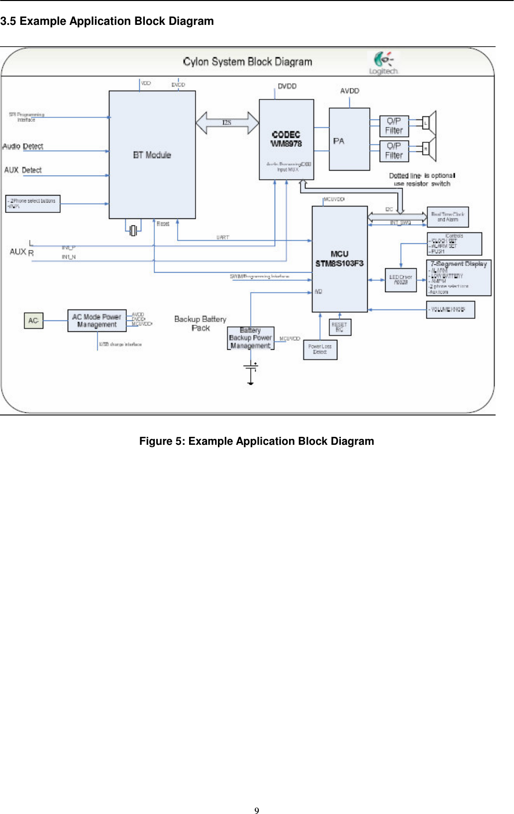
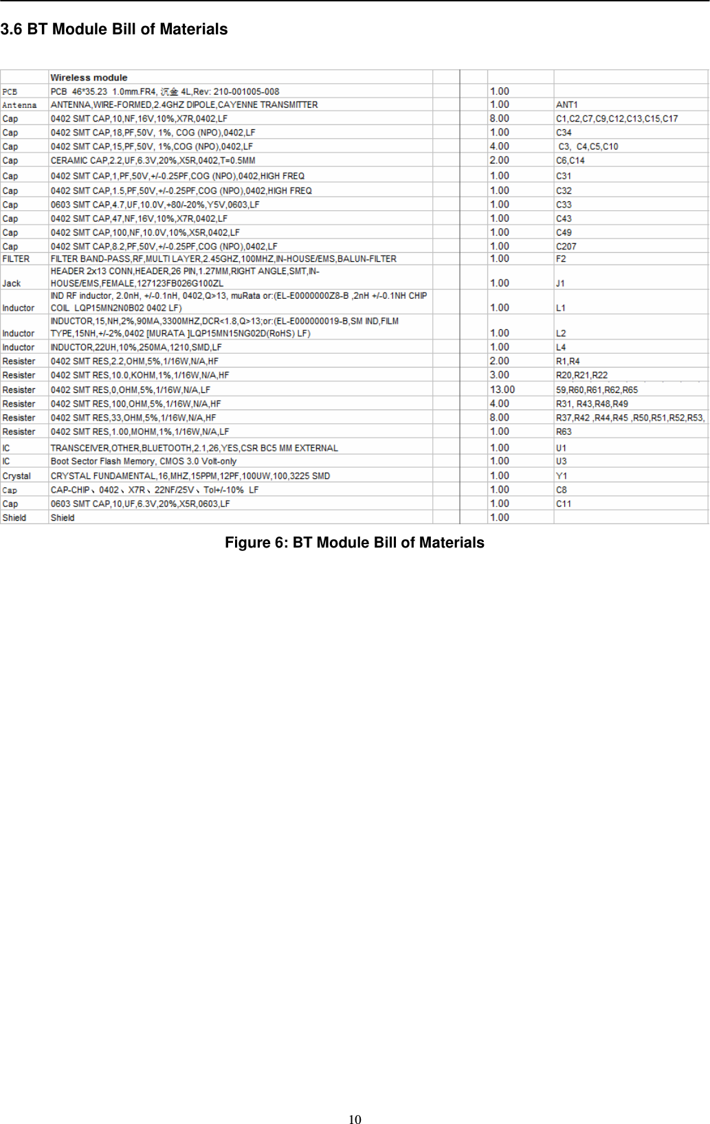
Logitech S00114 Wireless module User Manual July 20

Logitech Inc Wireless module July 20

User Manual July 20

                                                                                                  1  BC05 Flash BT Module     PRODUCT SPECIFICATION   PROJECT   Bluetooth Module  CUSTOMER                Logitech  REVISION   V1.0  DATE   Jul 12, 2011
                                                                                                  2TABLE OF CONTENTS   LIST OF TABLES…………………………………………………………………………………………………….…....3  LIST OF FIGURES………………………….……………………………………………………………………………..3   1.  Revision History ……………………………………………………………..……………………………….……..3  2.  Product Description and Specification………….………………………………………………….……….…...4   2.1 Product Description……….. ……………………………………………………………………......................4   2.2 References………………………………………….…………………………………………………..……….…4    3.    Hardware Description………………...........................................................................................................5 3.1 BC05 Block Diagram……….. ……………………………………………………………………...................5 3.2 BT PIN Configuration and Mechanical Dimension ………………………………………….…………….….6 3.3 BT PIN Description ………….. ……………………………………………………………………..................7 3.4 BT Module Schematics……………………………………………………………………………………...…8-9 3.5 Example Application Block Diagram……………………………………………………………………….…...9 3.6 BT Module Bill of Materials……………………………………………………………………………………..10  4.    FCC STATEMENT…………………………………………………………………………………………….……..11 5.    IC STATEMENT…………………………………………………………………………………………….….……..12
                                                                                                  3LIST OF TABLES  Table 1: Revision History ………………………………………………………………………………….……...3 Table 2: General Specification ……………………………………………………………………………..........4 Table 3: BT Pin Description …………………………………………………………………………….……......7    LIST OF FIGURES  Figure 1: BC05 Block Diagram………………………………………………………………………….……......5 Figure 2: Bluetooth Module Block Diagram ....…………………………………………………………………5 Figure 3: BT Pin Configuration and Mechanical Dimension …………………………………………….……6 Figure 4: BT Module Schematics………………………………………………………………………….……..8 Figure 5: Example Application Block Diagram …………………………………………………………………9 Figure 6: BT Module Bill of Materials………………………………………………………………….…….....10    1.  Reversion History  REVISION  PREPARED BY  DATE  DESCRIPTION   Rev 1.0    ZG Lou    12-Jul-2011  First Release                       Table 1: Revision History
                                                                                                  42.  Product description and specification This product is a Cost-effective single-chip stereo solution. Module used CSR BlueTunes Flash BGA BC57H687C chipset.    2.1 References   BlueCore5-Multimedia External CS-121064-DSP2  General Features     Fully Qualified Bluetooth v2.1 + EDR Specification System   Best-in-class Bluetooth Radio with 8dBm Transmit Power and -90dBm Receive Sensitivity   64MIPS Kalimba DSP Co-processor   16-bit Internal Stereo CODEC 95dB SNR for DAC   Low-power 1.5V Operation, 1.8V to 3.6V I/O   Integrated 1.5V and 1.8V Linear Regulators   Integrated Switched-mode Regulator   Integrated Battery Charger   USB, I2C and UART with Dual Port Bypass Mode to 4Mbits/s   Supports up to 32Mbit of External Flash Memory (8Mbit Typical Requirement)   Multi-Configurable I2S, PCM or SPDIF Interface   Enhanced Audibility and Noise Cancellation   8 x8 x 1.2mm, 0.5mm Pitch 169-ball LFBGA   Support for IEEE 802.11 Co-existence   Green (RoHS Compliant and no Antimony or Halogenated Flame Retardants)        2.2 Specifications  Table 2: BT Specifications Operating Frequency Band  2.4GHZ-2.48GHZ unlicensed ISM band Bluetooth Specification  V2.1+EDR Output Power Class  Class 2 RF Output Power ≦3.5dBm Dimension  46mm(L) X 35.23mm(W) X1.0mm(H)
                                                                                                  53. Hardware Description  3.1 BC05 Block Diagram  Figure 1: BC05 Block Diagram   Figure 2: BT Module Block Diagram
                                                                                                  63.2 BT Pin Configuration and Mechanical Dimension    # Pin  Pin label  # Pin    Function 1 VDD  2 ENC0 3 GND  4 ENC1 5 PCM_IN  6 SCL 7 PCM_OUT  8 SDA 9 PCM_SYNC 10 INPUT_CTRL 11 PCM_CLK  12 LD00 13 OTP_GDN  14 LD01 15 UART_RX  16 PWR_DET 17 UART_TX  18 AUDIO_DET 19 UART_CTS 20 SPKR_R_P 21 UART_RTS 22 SPKR_R_N 23 AIO0  24 SPKR_L_P 25 AIO1  26 SPKR_L_N  Figure 3: BT Pin Configuration and Mechanical Dimension
                                                                                                  73.3 BT Pin Description  Pin No.  Name  Type  Function  Remark 1  VDD  POWER  3.3V    2  ENC0  Output  Power amplifier standby  3  GND  Ground    Cround    connections  4  ENC1  OUTPUT  NC  5  PCM_IN  CMOS input, with weak internal pull-down.  I2S   6  SCL  OUTPUT  CHARGE MODE CONTROL  7  PCM_OUT  CMOS output, tri-state, with weak internal pull-down  I2S   8  SDA  OUTPUT  CHARGE MODE CONTROL  9  PCM_SYNC  Bi-directional with weak internal pull-down.  I2S   10  INPUT_CTRL OUTPUT  CHARGE MODE CONTROL  11  PCM_CLK  Bi-directional with weak internal pull-down.  I2S   12  LD00  OUTPUT  NC  13  OPT_GND  INPUT  REST  14  LD01  OUTPUT  NC  15  UART_RX  Bidirectional with weak  UART data input ,active high  16  PWR_DET  INPUT  NC  17  UART_TX  Output tri-state with weak  UART data output,active high  18  AUDIO_DET  Input  Audio detect pin  19  UART_CTS  COMS input with weak  UART clear to send active low  20  SPKR_R_P  OUTPUT  NC  21  UART_RTS  Bidirectional with weak  UART request to send active low  22  SPKR_R_N  OUTPUT  NC  23  AIO0  INPUT  NC  24  SPKR_L_P  OUTPUT  NC  25  AIO1  Bidirectional    NC  26  SPKR_L_N  OUTPUT  NC  14  GND 15  GND  Ground    Ground connections    Table 3: BT Pin Description
                                                                                                  83.4 BT Module Schematics     Figure 4: BT Module Schematics
                                                                                                  93.5 Example Application Block Diagram    Figure 5: Example Application Block Diagram
                                                                                                  10 3.6 BT Module Bill of Materials   Figure 6: BT Module Bill of Materials
                                                                                                  11 4.0 FCC STATEMENT Federal Communications Commission (FCC) Statement 15.21 You  are  cautioned  that  changes  or  modifications  not  expressly  approved  by  the  part  responsible  for compliance could void the user’s authority to operate the equipment.  15.105(b) This equipment has been tested and found to comply with the limits for a Class B digital device, pursuant to part  15  of  the  FCC  rules.  These  limits  are  designed  to  provide  reasonable  protection  against  harmful interference in a residential installation. This equipment generates, uses and can radiate radio frequency energy and, if not installed and used in accordance with the instructions, may cause harmful interference to radio  communications.  However,  there  is  no  guarantee  that  interference  will  not  occur  in  a  particular installation. If this equipment does cause harmful interference to radio or television reception, which can be determined by turning the equipment off and on, the user is encouraged to try to correct the interference by one or more of the following measures: - Reorient or relocate the receiving antenna. - Increase the separation between the equipment and receiver. - Connect the equipment into an outlet on a circuit different from that to which the receiver is connected. - Consult the dealer or an experienced radio/TV technician for help.  Operation is subject to the following two conditions: 1) This device may not cause interference and 2) This device must accept any interference, including interference that may cause undesired operation of the device.  FCC RF Radiation Exposure Statement: This equipment complies with FCC radiation exposure limits set forth for an uncontrolled environment. End users must follow the specific operating instructions for satisfying RF exposure compliance. This transmitter must not be co-located or operating in conjunction with any other antenna or transmitter. According to FCC Regulations, the distance from the antenna to the user body must be minimum 20cm when the terminal is printing state.  Note: Please  notice that  if  the FCC/IC  identification number  is  not  visible  when  the  module  is  installed  inside another device, then the outside of the device into which the module is installed must also display a label referring  to  the  enclosed  module.  This  exterior  label  can  use  wording  such  as  the  following:  “Contains Model:  S-00114,  Contains  FCC  ID:  DZLS00114,  Contains  IC:  1807D-S00114”  Any  similar  wording  that expresses the same meaning may be used.
                                                                                                  12  5.0 IC STATEMENT   This device complies with Part 15 of the FCC Rules and Industry Canada licence-exempt RSS standard(s). Operation is subject to the following two conditions: (1) this device may not cause harmful interference, and (2) this device must accept any interference received, including interference that may cause undesired operation. (French) L’appareil est conforme à la réglementation FCC, section 15 et Industrie Canada RSS standard exempts de licence  (s).  Son  utilisation  est  soumise  à  deux  conditions:  (1)  L’appareil  ne  doit  pas  provoquer d’interférences  nuisibles,  et  (2)  L’appareil  doit  supporter  les  interférences  reçues,  y  compris  les interférences empêchant son fonctionnement correct.

Navigation menu