LongSung Technology U5501 HSDPA Module User Manual U5501
LongSung Technology (Shanghai)Co.,Ltd. HSDPA Module U5501
User Manual
U5501_Hardware_User_Guide_V2.3 Page 1 of 59
U5501_Hardware_User_Guide _V2.3

U5501_Hardware_User_Guide_V2.3 Page 2 of 59
IMPORTANT NOTICE
COPYRIGHT NOTICE
Copyright©2010, LongSung Technology (Shanghai) Co., Ltd. All rights
reserved.
TRADEMARKS
LongSung Technology (Shanghai) Co., Ltd’s products are exclusively owned by
LongSung Technology (Shanghai) Co., Ltd. References to other companies and
their products use trademarks owned by the respective companies and are for
reference purpose only.
CONFIDENTIALITY
The information contained here (including any attachments) is confidential. The
recipient here acknowledges the confidentiality of this document, and except for
the specific purpose, this document shall not be disclosed to any third party.
WARRANTY DISCLAIMER
LongSung Technology (Shanghai) Co., Ltd makes no representations or
warranties, either express or implied, by or with respect to anything in this
document, and shall not be liable for any implied warranties of merchantability
or fitness for a particular purpose or for any indirect, special or consequential
damages.
NO GUARANTEE
Our company will not take any responsibility for any damage caused by the
customer’s abnormal operation. Please refer to specification and designing
reference guide. Our company have right to modify the document according to
technical requirement with no announcement to the customer.

U5501_Hardware_User_Guide_V2.3 Page 3 of 59
CAUTION: U5501 HSDPA module is an ESD (electrostatic discharge) sensitive
device. Electrostatic charges as high as 1 K Volts readily accumulate on the
human body and test equipment and can discharge without detection.
Permanent damage may occur on devices subjected to high-energy
electrostatic discharges. Therefore, proper ESD precautions are recommended
to avoid performance degradation or loss of functionality.
Warning:
The U5501 module is designed to comply with the FCC statements.FCC ID is
XHZU5501.The Host system using U5501 should indicated “Contains FCC ID:
XHZU5501”.
This device complies with part 15B of the FCC rules. Operation is subject to the
following two conditions:
(1) this device may not cause harmful interference
(2) this device must accept any interference, including interference that may
cause undesired operation.
Changes or modifications to this unit not expressly approved by the party
responsible for compliance could void the user's authorityto operate the
equipment.
This equipment complies with FCC/IC radiation exposure limits set forth for an
Uncontrolled environment.This equipment should be installed and operated
with minimum distance 20cm between the radiator and your body as well as
kept minimum 20cm from radio antenna depending on the portable or Mobile
status of this module usage.
The manual of the host system,which use U5501 must include RF exposure
warning statement to advice user should keep minimum 20cm from the radio
antenna of U5501 module depending on Mobile status.
The U5501 module can not be installed with other radio .such as co-located or
operating in conjunction with any other antenna or transmitter.
Antenna Type: Connector
Antenna Gain: GSM850:1.2dBi;GSM1900:1.2dBi.

U5501_Hardware_User_Guide_V2.3 Page 4 of 59
Contents
1. Overview ..................................................................................................................................8
1.1. Purpose of the document.......................................................................................8
1.2. Summary......................................................................................................................8
1.3. Correlative documents ............................................................................................8
1.4. Document’s history...................................................................................................9
1.5. Abbreviations..............................................................................................................9
2. Introduction...........................................................................................................................11
2.1. Key features..............................................................................................................13
2.2. Operating modes.....................................................................................................15
2.3. Hardware functional block diagram .................................................................16
3. Application interfaces description.................................................................................18
3.1. 116-pin LGA PAD.....................................................................................................18
3.2. Power supply.............................................................................................................22
3.2.1. Power Supply and reference design.....................................................22
3.2.1.1. VBAT input .........................................................................................22
3.2.1.2. VRTC input .........................................................................................23
3.2.1.3. VOUT voltage output......................................................................24
3.2.1.4. POWER_ON_OFF input ..................................................................24
3.2.1.5. RESET_N input .................................................................................25
3.2.2. Power on/off time sequence ...................................................................26
3.2.2.1. Power on time sequence ..............................................................26
3.2.2.2. Normal power off time seqence.................................................26
3.2.2.3. Low power to power off ................................................................27
3.2.3. Reset time sequence..................................................................................27
3.3. USB interface............................................................................................................28
3.3.1. USB interface description.........................................................................28
3.3.2. USB reference circuit .................................................................................28
3.3.3. USB driver......................................................................................................29
3.3.3.1. Linux OS load USB driver for U5501 .......................................30
3.3.3.2. Linux OS AP use AT to control U5501 .....................................32
3.3.3.3. Linux OS AP dial PPP connection...............................................34
3.4. UART interface..........................................................................................................37
3.4.1. UART interface description ......................................................................37
3.4.2. UART interface reference circuit............................................................37
3.4.3. UART interface description ......................................................................38
3.5. U5501 sleep and wakeup control......................................................................38
3.6. Analog audio interface ..........................................................................................39
3.6.1. Analog audio interface description .......................................................39
3.6.2. Hands-free channel ....................................................................................39

U5501_Hardware_User_Guide_V2.3 Page 5 of 59
3.6.3. Handset channel..........................................................................................39
3.6.4. Analog audio reference circuit................................................................40
3.7. PCM interface............................................................................................................41
3.7.1. PCM interface description.........................................................................42
3.7.2. Auxiliary PCM................................................................................................42
3.7.3. Primary PCM..................................................................................................44
3.8. USIM/SIM interface ................................................................................................45
3.8.1. USIM/SIM interface description.............................................................45
3.8.2. USIM/SIM interface reference circuit ..................................................46
3.9. Status indicator interface.....................................................................................48
3.9.1. Status indicator description ....................................................................48
3.9.2. Status indicator reference circuit..........................................................49
3.10. GPIO ..........................................................................................................................50
3.11. Antenna interface .................................................................................................50
3.11.1. Solder antenna ..........................................................................................50
3.11.2. RF connector...............................................................................................51
3.11.2.1. RF cable ............................................................................................52
3.11.3. U5501 RF output power .........................................................................52
3.11.4. U5501 RF receiver sensitivity ..............................................................52
3.11.5. U5501 operating frequencies...............................................................53
3.11.6. Antenna parameters requirement......................................................53
4. Mechanics...............................................................................................................................54
4.1. The view of U5501..................................................................................................54
4.2. 3D stack......................................................................................................................54
4.3. 2D mechanical dimensions..................................................................................55
4.4. Application side library of U5501......................................................................55
5. Power consumption ............................................................................................................56
6. Electrical characteristics ...................................................................................................57
6.1. Absolute maximum power ratings....................................................................57
6.2. Operating temperatures .......................................................................................57
6.3. Interface operating status ...................................................................................58
6.4. Reliability....................................................................................................................58
6.5. Electrostatic discharge ..........................................................................................59

U5501_Hardware_User_Guide_V2.3 Page 6 of 59
Tab les
Table 1:Document’s update history...........................................................................9
Table2:Abbreviation and description ........................................................................9
Table3:Key features of U5501...................................................................................13
Table4:Overview operating modes ..........................................................................15
Table5:U5501116-pin LGA PAD pin definition.....................................................19
Table6:U5501 Power supply correlative interfaces ...........................................22
Table7:U5501 USB interface ......................................................................................28
Table8:U5501 UART interface ....................................................................................37
Table9:U5501 sleep and wakeup interface...........................................................38
Table10 :U5501 analog audio interface description ...........................................39
Table11 :U5501 second channel audio....................................................................39
Table12 :U5501 first channel audio..........................................................................40
Table13 :Auxiliary PCM and Primary PCM configuration...................................41
Table14 :U5501 PCM interface ...................................................................................42
Table15 :AUX_CODEC time sequence parameters .............................................43
Table16 :PRIM_CODEC time sequence parameters............................................45
Table17 :U5501 USIM/SIM interface ........................................................................45
Table18 :U5501 status indicator description.........................................................49
Table19 :U5501 status indicator description.........................................................49
Table20 :U5501 GPIOs ..................................................................................................50
Table21 :U5501 antenna interface............................................................................50
Table22 :U5501 RF output power..............................................................................52
Table23 :U5501 RF receiver sensitivity...................................................................52
Table24 :U5501 operating frequencies ...................................................................53
Table25 :U5501 antenna parameters requirement ............................................53
Table26 :U5501 max current consumption in some mode..............................56
Table27 :Absolute maximum power ratings..........................................................57
Table28 :U5501 module operating temperature .................................................57
Table29 :Digital Signal DC Characteristics.............................................................58
Table30 :U5501 power supply range .......................................................................58
Table31 :Requirements on the environment reliability.....................................58
Table32 :The ESD endure status measured table...............................................59

U5501_Hardware_User_Guide_V2.3 Page 7 of 59
Figures
Figure1:U5501 Hardware functional block diagram .........................................16
Figure2:U5501 116-pin LGA PAD pins sign..........................................................18
Figure3:U5501 Power supply VBAT input .............................................................23
Figure4:VRTC connect to rechargeable battery..................................................23
Figure5:VRTC connect to non-rechargeable battery ........................................24
Figure6:VRTC connect to large capacitance capacity.......................................24
Figure7:POWER_ON_OFF reference circuit ..........................................................25
Figure8:RESET control module reset......................................................................25
Figure9:power on time sequence.............................................................................26
Figure10:U5501 power off time sequence ...........................................................27
Figure11:U5501 RESET time sequence .................................................................27
Figure12:U5501 USB reference circuit ..................................................................28
Figure13:U5501 UART connection...........................................................................38
Figure14:U5501 analog audio reference circuit .................................................40
Figure15:AUX_PCM_SYNC time sequence............................................................42
Figure16:AUX_PCM_CODEC to U5501 time sequence.....................................43
Figure17:U5501 to AUX_PCM_CODEC time sequence.....................................43
Figure18:PRIM_PCM_SYNC time sequence..........................................................44
Figure19:PRIM_PCM_CODEC to U5501 time sequence...................................44
Figure20:U5501 to PRIM_PCM_CODEC time sequence...................................44
Figure21:The SPEC of C707 10M006 512 2 SIM Holder.................................47
Figure22:U5501 USIM/SIM interface reference circuit....................................48
Figure23:U5501 status indicator reference circuit............................................49
Figure24:U5501 solder antenna reference circuit.............................................51
Figure25:U5501 RF connector reference circuit.................................................51
Figure26:The view of U5501......................................................................................54
Figure27:U5501 2D mechanical dimensions .......................................................55

U5501_Hardware_User_Guide_V2.3 Page 8 of 59
1. Overview
U5501 is a wireless module which is designed for the global market. It is a
consumptive product; it can be designed in many kinds of applications which
can work on HSDPA/UMTS/EDGE/GPRS/GSM network.
On HSDPA network in the world, U5501 enables connection to the Internet at DL
data speed up to 3.6Mbps. In areas where HSDPA service is not available,
U5501 still enables reliable and secure data connections over UMTS at speed up
to 384 Kbps or EDGE at speed up to 237Kbps or GPRS at speed up to 85.6Kbps.
U5501 provides Audio, SMS, Phonebook functions as well as high speed access.
It can be designed in many kinds of applications. Such as Video monitor, Tablet,
Electric-book, MID, Vehicle equipment, etc.
1.1. Purpose of the document
The document described the basic functions, supported services, the key
features, main interfaces and reference design, the mechanics and the
electronic characteristics of the module U5501. It will guide the user to design
U5501 in their applications.
1.2. Summary
The following lists the contents of this document.
Chapter 1: Described the overview, purpose, correlative documents,
document’s history and abbreviations.
Chapter 2: Described the basic functions, key features and hardware
interfaces of the module.
Chapter 3: Described in detail the module’s interfaces and reference design.
Chapter 4: Described the mechanical specifications of the module.
Chapter 5: Described in detail the power consumptions of the module.
Chapter 6: Described in detail electrical specifications of the module.
1.3. Correlative documents
U5501_SPEC
U5501_ATC

U5501_Hardware_User_Guide_V2.3 Page 9 of 59
U5501_EVB_User_Guide
U5501_Reference_Circuit
U5501_Application_Guide
1.4. Document’s history
Table 1:Document’s update history
Version Author Release Time Description
V2.3 Huaming Zhang 2012-7-24 V2.3 create
1.5. Abbreviations
Table2:Abbreviation and description
Abbreviations Description
AMR Adaptive Multi-rate
BER Bit Error Rate
BTS Base Transceiver Station
PCI Peripheral Component Interconnect
CS Circuit Switched (CS) domain
CSD Circuit Switched Data
DCE Data communication equipment
DTE Data terminal equipment
DTR Data Terminal Ready
EDGE Enhanced Data rates for GSM Evolution
EFR Enhanced Full Rate
EGSM Enhanced GSM
EMC Electromagnetic Compatibility
ESD Electrostatic Discharge
FR Frame Relay
GMSK Gaussian Minimum Shift Keying
GPIO General Purpose Input Output
GPRS General Packet Radio Service
GSM Global Standard for Mobile Communications
HR Half Rate
HSDPA High Speed Downlink Packet Access

U5501_Hardware_User_Guide_V2.3 Page 10 of 59
HSUPA High Speed Uplink Packet Access
HSPA HSPA High-Speed Packet Access
IEC International Electro-technical Commission
IMEI International Mobile Equipment Identity
I/O Input/Output
ISO International Standards Organization
ITU International Telecommunications Union
bps bits per second
LED Light Emitting Diode
M2M Machine to machine
MO Mobile Originated
MT Mobile Terminated
NTC Negative Temperature Coefficient
PC Personal Computer
PCB Printed Circuit Board
PCS Personal Cellular System
PCI Peripheral Component Interconnect
PCM Pulse Code Modulation
PCS Personal Communication System
PDU Packet Data Unit
PPP Point-to-point protocol
PS Packet Switched
QPSK Quadrate Phase Shift Keying
SIM Subscriber Identity Module
TCP/IP Transmission Control Protocol/ Internet Protocol
UART Universal asynchronous receiver-transmitter
USIM Universal Subscriber Identity Module
UMTS Universal Mobile Telecommunications System
USB Universal Serial Bus
WCDMA Wideband Code Division Multiple Access

U5501_Hardware_User_Guide_V2.3 Page 11 of 59
2. Introduction
U5501 is a wireless module which is designed for the global market. It is a
consumptive product; it can be designed in many kinds of applications which
can work on HSDPA/UMTS/EDGE/GPRS/GSM network.
U5501 support the Bands as the following:
Dual-Band UMTS(WCDMA/FDD):900/2100 MHz;
Quad-Band GSM :850/900/DCS1800/PCS1900 MHz。
On HSDPA network in the world, U5501 enables connect to the Internet at DL
data speed up to 3.6Mbps. In areas where HSDPA service is not available,
U5501 still enables reliable and secure data connections over UMTS at speed up
to 384 Kbps or EDGE at speed up to 237Kbps or GPRS at speed up to 85.6Kbps.
U5501 provides Audio, SMS, Phonebook functions as well as high speed access.
It can be designed in many kinds of applications. Such as Video monitor, Tablet,
Electric-book, MID, Vehicle equipment, etc.
U5501 integrates the RF and Baseband onto one small PCB. It can fulfill all the
functions of RF signal receiving and transmitting, Baseband signal processing
and audio signal processing so that the customers can realize all kinds of their
own wireless products with very few peripheral components.
Designed on a single-side PCB, U5501 has a tiny dimension of
30.0mm×30.0mm×2.5mm, with a LGA PAD interface, which provides all
hardware interfaces between the module and customers’ boards. The main
hardware interfaces of U5501 consist of power supply interfaces, USB interface,
UART interfaces, USIM/SIM interface, Audio interfaces, PCM interface, ADC
interface, VRTC interface and GPIO.
U5501 is integrated with the TCP/IP protocol, it not only supports standard AT
(Complied with Hayes 3GPP TS 27.007 and 27.005), but also support Longsung
extended AT commands, which are very suited for developing all kinds of the
customized applications.
U5501 provide main interfaces for applications, the interfaces as the
following:
1) Power interface
2) USB interface

U5501_Hardware_User_Guide_V2.3 Page 12 of 59
3) UART interface
4) USIM/SIM interface
5) Analog audio interface
6) PCM interface
7) GPIO
8) RESET interface
9) Power on off interface
10) Work status indicator
11) RTC interface
12) Voltage ourput
13) Antenna interface

U5501_Hardware_User_Guide_V2.3 Page 13 of 59
2.1. Key features
Table3:Key features of U5501
Feature Description
Power supply 3.3V~4.2V(Typical 3.8V)
Frequency Bands UMTS: Dual-Band, 900/2100MHz
EDGE/GPRS/GSM: Quad-Band, 850/900/1800/1900MHz
HSDPA DL:3.6Mbps
UMTS UMTS PS: 384 kbps(DL), 384 kbps(UL)
UMTS CS: 64 kbps(DL), 64 kbps(UL)
EDGE
EDGE: Class12, 236.8kbps(DL), 118kbps(UL)
Mobile station class B
Coding schemes: MCS1-9
GPRS
GPRS: Class12,85.6kbps(DL),42.8kbps(UL)
Mobile station class B
Coding schemes: CS1-4
Support Full PBCCH
Data
CSD GSM CSD:9.6kbps
Voice
Triple-rate codec for HR、FR、EFR
Support AMR
Support DTMF
Caller identification, Call forwarding, Call holding, Call
waiting and Three party service
SMS
Point to point MO、MT
SMS cell broadcast
Support Text and PDU mode
Temperature
Normal operation: -20℃~+65℃
Restricted Operation: -30℃~+75℃
Storage temperature: -40℃~+85℃
ESD
VBAT, GND: Air discharge ±8KV,Contact discharge ±4KV
RF interface: Air discharge ±8KV,Contact discharge ±4KV
Else ports: Air discharge ±4KV, Contact discharge±2KV
Max power RF transition
Class 4 (2 W) for GSM850/GSM900
Class 1 (1 W) for GSM1800/GSM1900
Class E2 (0.5 W) for EDGE900
Class E2 (0.4 W) for EDGE1800
Class 3 (0.25 W) for UMTS
Current consumption
Power off mode:50μA
Sleep mode:<4mA
Idle mode:<40mA

U5501_Hardware_User_Guide_V2.3 Page 14 of 59
Voice mode:<300mA
Data mode:<600mA
Application interface LGA PAD
LGA PAD
Power interface
1 USB2.0 High-Speed interface
1 UART interface
1 USIM/SIM interface(Compatible 3V&1.8V)
2 analog audio compatible
1 PCM interface
1 RESET interface
2 NETLIGHT ourput interface
2 voltage output(2.6V & 1.8V)
1 power on off interface
1 VRTC
12 GPIOs(2 of them voltage are 1.8V, the others are
2.6V)
2 sleep and wakeup GPIOs
Antenna interface
Dimensions 30.0mm×30.0mm×2. 5mm
Weight <8g
Fixed structure Solder with LGA PAD
AT command Standard AT commands (Hayes 3GPP TS 27.007 and 27.005)
Support LongSung Extend AT commands
Approvals RoHS

U5501_Hardware_User_Guide_V2.3 Page 15 of 59
2.2. Operating modes
Table4:Overview operating modes
Mode Function
Sleep mode Set WAKEUP_IN to low, the U5501 will enter to sleep mode, the module
will reduce the current consumption to minimal level.
GSM IDLE Software is active. Module has registered to the GSM
network, and the module is ready to send and receive.
GSM mode
GSM TALK
Connection is going on between two subscribers. In
this case, the power consumption depends on network
settings.
GPRS IDLE
Module is ready for GPRS data transfer, but no data is
currently sent or received. Power consumption
depends on network settings and GPRS configuration
(e.g. multi-slot settings).
GPRS mode
GPRS DATA
GPRS data transfer in progress. Power consumption
depends on network settings (e.g. power control
level), uplink/downlink data rates and GPRS
configuration (e.g. used multi-slot settings).
EDGE IDLE
Module is ready for EDGE data transfer, but no data is
currently sent or received. Power consumption
depends on network settings and EDGE configuration
(e.g. multi-slot settings).
EDGE mode
EDGE DATA
EDGE data transfer in progress. Power consumption
depends on network settings (e.g. power control
level), uplink/downlink data rates and EDGE
configuration (e.g. used multi-slot settings).
WCDMA IDLE
Software is active. Module has registered to the
WCDMA network, and the module is ready to send and
receive.
WCDMA TALK Module is serving in audio. The power consumption
depends on WCDMA network settings.
WCDMA mode
WCDMA DATA
WCDMA data transfer in progress. Power consumption
depends on network settings (e.g. power control
level), uplink/downlink data rates and WCDMA
configuration.
Minimum
Function mode
VBAT remains applied.
Use AT+CFUN=0 to let module go into Minimum Function mode
Power Down Module will go to power off mode when:
U5501_Hardware_User_Guide_V2.3 Page 16 of 59
1. Send AT^SMSO
2. VBAT to low
3. Press the POWER_ON_OFF to power off module.
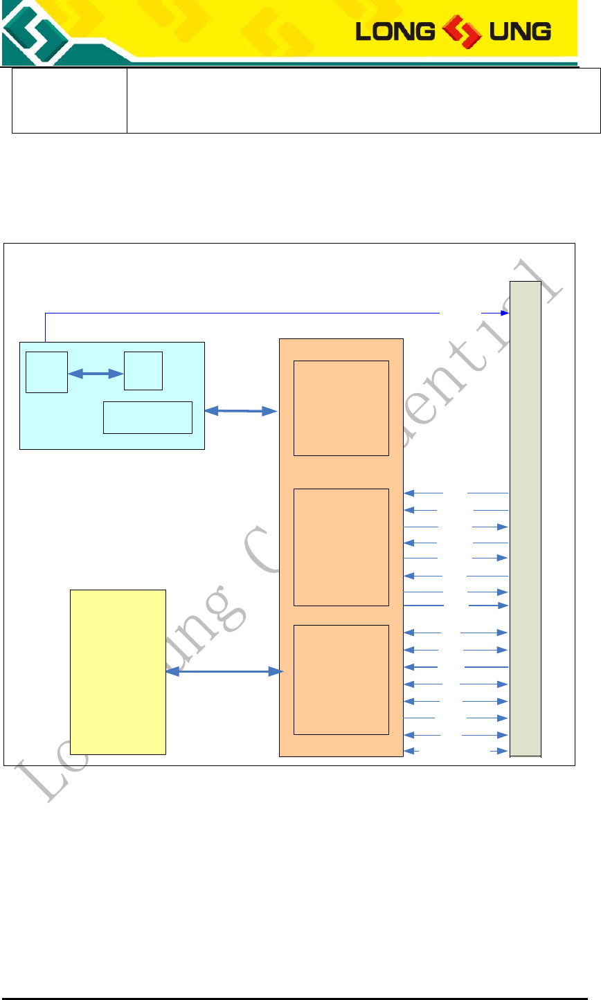
2.3. Hardware functional block diagram
LGA Interface
SW PA
RF Block VCTCXO
NAND FLASH
&SDRAM
RF
transceiver
Analog
Baseband
Digital
Baseband
RESET
USB
USIM
Netlight
GPIO
VBAT
UART
Micphone1
Earphone
PCM
1.8V
ANT
Micphone2
Speaker
VRTC
2.6V
Sleep and wakeup
Figure1:U5501 Hardware functional block diagram
☆ RF include:
1) WCDMA Transceiver
2) GSM Transceiver
3) SW
4) VCTCXO
☆ Baseband include:
1) PMU
2) Audio process unit
3) Digital Baseband chip

U5501_Hardware_User_Guide_V2.3 Page 17 of 59
4) NAND FLASH and SDRAM
U5501_Hardware_User_Guide_V2.3 Page 18 of 59
3. Application interfaces description
3.1. 116-pin LGA PAD
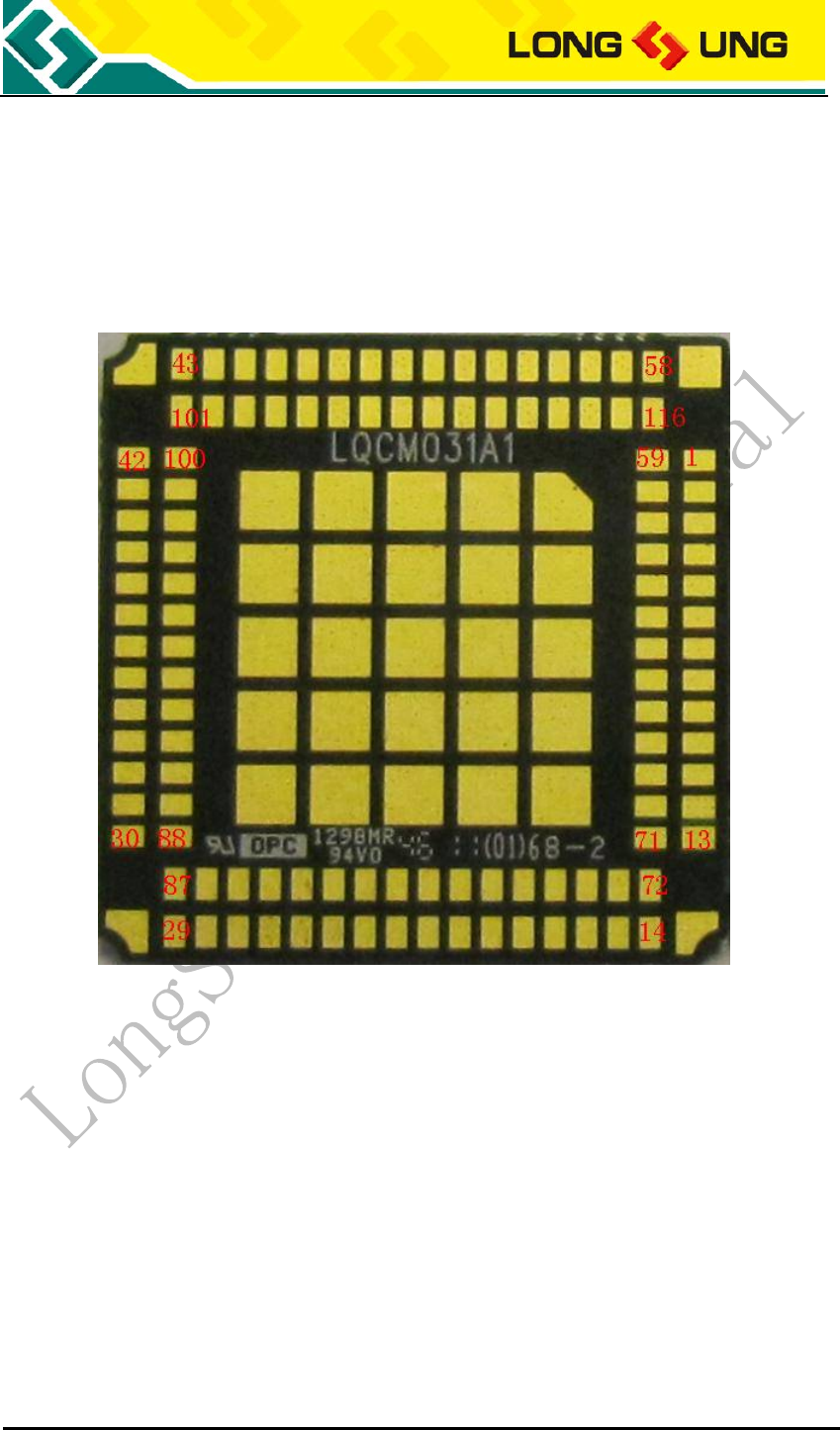
Figure2:U5501 116-pin LGA PAD pins sign

U5501_Hardware_User_Guide_V2.3 Page 19 of 59
Table5:U5501116-pin LGA PAD pin definition
PIN NO. PIN Name I/O Describe
1 NC - -
2 NC - -
3 NC - -
4 NC - -
5 PCM_SYNC I/O PCM interface sync(2.6V)
6 PCM_DIN I PCM I/F data in(2.6V)
7 PCM_DOUT O PCM I/F data out(2.6V)
8 PCM_CLK I/O PCM interface clock(2.6V)
9 NC - -
10 NC - -
11 WAKEUP_IN I External system wakeup module(2.6V)
12 VBAT I Power supply input(3.3V~4.2V, typical 3.8V/1A
13 VBAT I Power supply input(3.3V~4.2V, typical 3.8V/1A
14 NC - -
15 GPIO_2.6V I/O 2.6V
16 NC - -
17 NC - -
18 NC - -
19 NC - -
20 NC - -
21 NC - -
22 NC - -
23 NC - -
24 NC - -
25 NC - -
26 NC - -
27 NC - -
28 GPIO_1.8V I/O 1.8V
29 GPIO_1.8V I/O 1.8V
30 NC - -
31 VCC_EXT_2.6V O 2.6V power output(20Ma)
32 VCC_EXT_1.8V O 1.8V power output(20mA)
33 NC - -
34 SIM_VCC O Power supply for SIM card(1.8V/2.85V)
35 VRTC I VRTC input(1.5V~3.25V, typical 3.0V)
36 NC - -
37 NC - -
38 MIC2_P I Positive pole of the input of audio interface 2
39 MIC2_N I Negative pole of the input of audio interface 2

U5501_Hardware_User_Guide_V2.3 Page 20 of 59
PIN NO. PIN Name I/O Describe
40 MIC1_P I Positive pole of the input of audio interface 2
41 MIC1_N I Negative pole of the input of audio interface 2
42 NC - -
43 GPIO_2.6V I/O 2.6V
44 GPIO_2.6V I/O 2.6V
45 GPIO_2.6V I/O 2.6V
46 GPIO_2.6V I/O 2.6V
47 NC - -
48 GND - -
49 GND - -
50 GND - -
51 GPIO_2.6V I/O 2.6V
52 GND - -
53 GND - -
54 GND - -
55 GPIO_2.6V I/O 2.6V
56 GND - -
57 GND - -
58 GND - -
59 GND - -
60 NC - -
61 NC - -
62 NC - -
63 NC - -
64 NC - -
65 NC - -
66 NC - -
67 NC - -
68 NC - -
69 NC - -
70 SIM_DET I/O SIM card insert or remove detect(2.6V)
71 WAKEUP_OUT O Module wakeup the external system(2.6V)
72 NC - -
73 UART_DSR O UART data set ready(2.6V)
74 UART_RTS O UART ready for receive(2.6V)
75 UART_DCT O UART data carrier detect(2.6V)
76 UART_TX O UART transmit data output(2.6V)
77 UART_RING O UART ring indicator(2.6V)
78 UART_RX I UART receive data input(2.6V)
79 UART_DTR I UART data terminal ready(2.6V)

U5501_Hardware_User_Guide_V2.3 Page 21 of 59
PIN NO. PIN Name I/O Describe
80 UART_CTS I UART clear to send(2.6V)
81 POWER_ON_OFF I System power on or power off
82 NC - -
83 NC - -
84 NC - -
85 USB_DM I/O USB 2.0 high speed D-
86 USB_DP I/O USB 2.0 high speed D+
87 NC - -
88 SIM_RESET O SIM reset
89 SIM_DATA I/O SIM data
90 SIM_CLK O SIM clock
91 LED_STATUS O Status indicator(Drive current: 10mA)
92 NC - -
93 NC - -
94 NC - -
95 NC - -
96 EAR_OUT_N O Negative pole of the output of earphone
97 EAR_OUT_P O Positive pole of the output of earphone
98 SPKR_OUT_P O Positive pole of the output of speaker
99 SPKR_OUT_N O Negative pole of the output of speaker
100 RESET_N I Reset module(1.8V)
101 LED_MODE O Mode indicator(Drive current: 10mA)
102 NC - -
103 NC - -
104 NC - -
105 GPIO_2.6V I/O 2.6V
106 GND - -
107 MAIN_ANT - RF main antenna interface
108 GND - -
109 GPIO_2.6V I/O 2.6V
110 GND - -
111 NC - -
112 GND - -
113 GPIO_2.6V I/O 2.6V
114 GND - -
115 NC - -
116 GND - -

U5501_Hardware_User_Guide_V2.3 Page 22 of 59
3.2. Power supply
U5501 power on and power off correlative interfaces as the following:
Table6:U5501 Power supply correlative interfaces
PIN Name I/O PIN No. 描述
VBAT I 12,13 Power supply ,3.3V~4.2V ,
typical 3.8V
VRTC I 35 1.5~3.25,typical 3.0V
VCC_EXT_1.8V O 32 Voltage output,1.8V,20mA
VCC_EXT_2.6V O 31 Voltage output,2.6V,20mA
POWER_ON_OFF I 81 Power on off control, low active
RESET I 100 Reset,1.8V,low active
GND
48~50,52~59,106,108,
110,112,114,116 GND
3.2.1. Power Supply and reference design
3.2.1.1. VBAT input
The power supply of U5501 should be a single voltage source with VBAT ranged
from 3.3V to 4.2V. As a mobile terminal conformed to the HSDPA/UTMS/GSM
criterions, in some case, the ripple in a transmit burst may cause a maximum
voltage drop of 450mV while the current consumption will rise to the typical
peak of 2A. So the power supply must be able to provide sufficient current.
The capacitor must be a larger one electrolytic capacity (recommend
2200uF/10V) or two smaller dimension tantalum capacities (470uF/6.3V) in
parallel (CA) is recommended. And with a small (0.1 µF to 1µF) ceramic (CB) in
parallel; the capacitors should put as close as possible to the U5501 VBAT pins.
U5501_Hardware_User_Guide_V2.3 Page 23 of 59
VBAT
CACB
+
Figure3:U5501 Power supply VBAT input
3.2.1.2. VRTC input
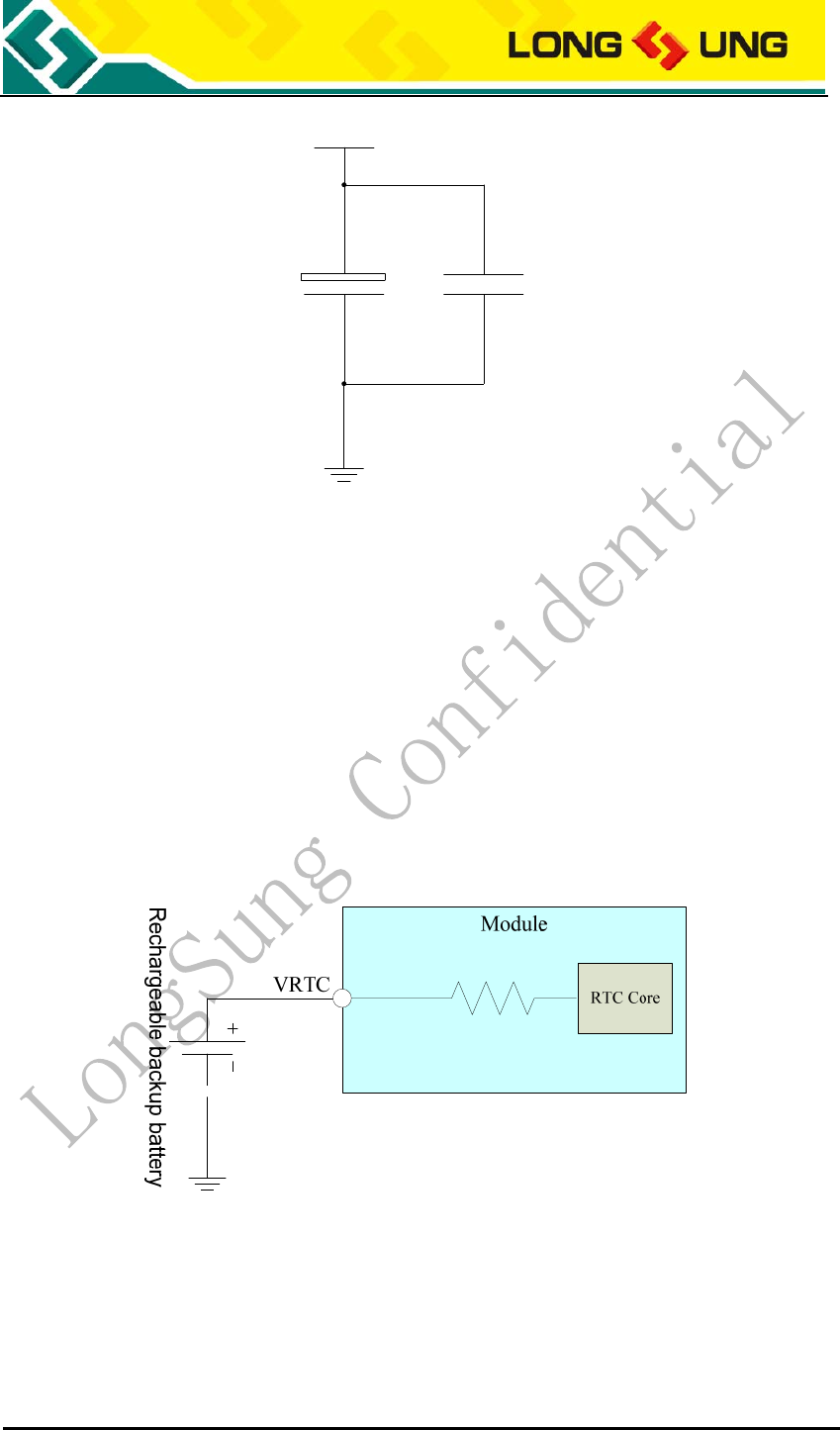
The PIN35 is VRTC interface.
VRTC can be used for connecting backup rechargeable battery. When VBAT
power supply is not available, the battery supplies the power to RTC core of
U5501. When VBAT is available, U5501 can recharge the battery via VRTC pin.
If the RTC is useless for you, you can set PIN51 as NC.
Reference design as the following:
Figure4:VRTC connect to rechargeable battery
If use non-rechargeable battery, the reference design as the following:
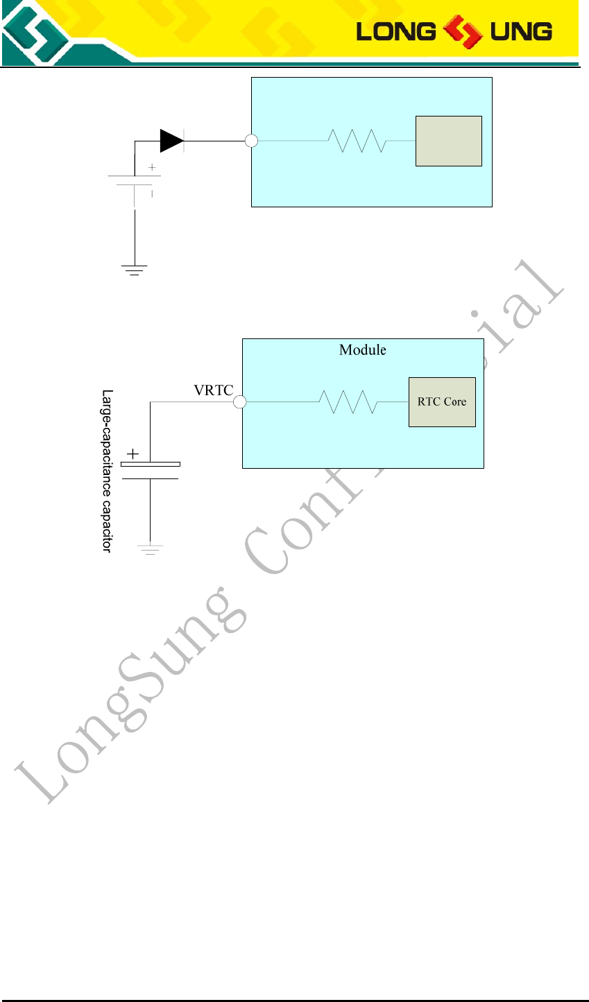
U5501_Hardware_User_Guide_V2.3 Page 24 of 59
VRTC
Module
Non-rechargeable battery
RTC Core
Figure5:VRTC connect to non-rechargeable battery
If use a large capacitance capacity, the reference design as the following:
Figure6:VRTC connect to large capacitance capacity
3.2.1.3. VOUT voltage output
During U5501 working, 2.6V voltage will output through PIN31 and 1.8V voltage
will output through PIN32, which named VCC_EXT_2.6V and VCC_EXT_1.8V.
The current is rated for 20mA. They can be used as a power supply of the
external device, such as LCD. And you can read the level of VCC_EXT_2.6V to
judge whether the module is working.
3.2.1.4. POWER_ON_OFF input
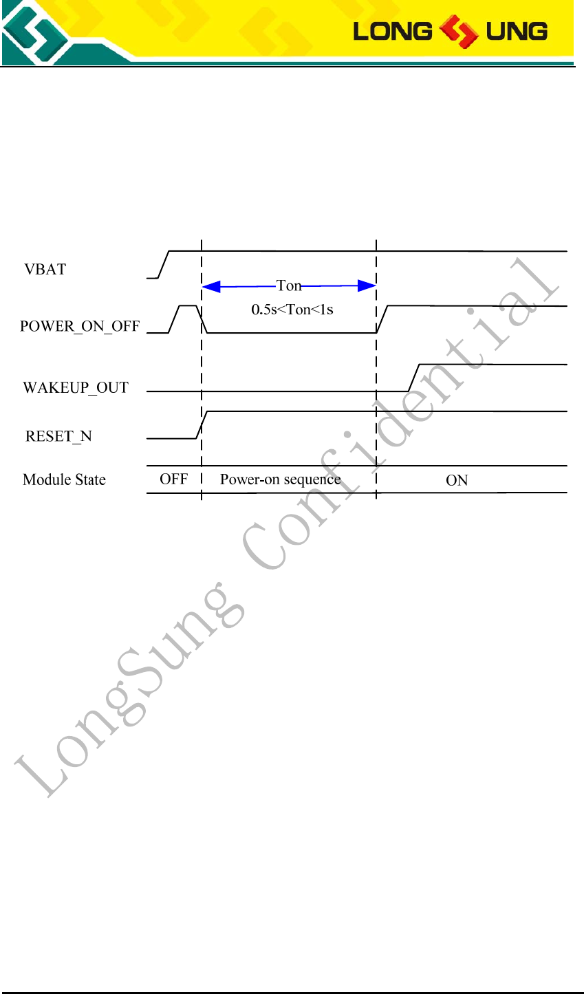
The POWER_ON_OFF (PIN81) is used to control U5501 power on and power off.
When module is power off, pull down POWER_ON_OFF for at least 0.5s, the
module is powered on;
When module is power on, pull down POWER_ON_OFF for at least 2.5s
again, the module is powered off.
U5501_Hardware_User_Guide_V2.3 Page 25 of 59
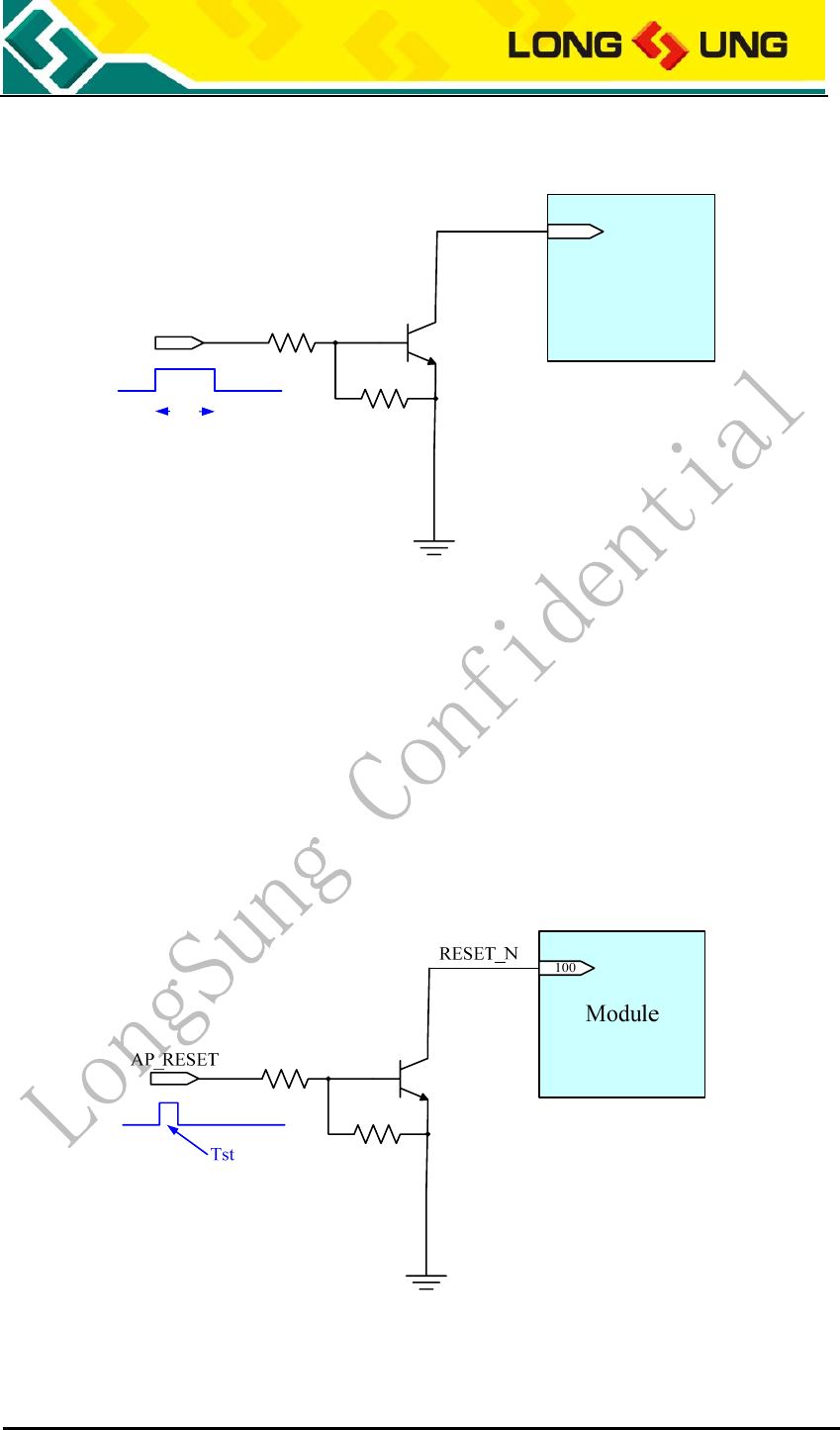
The reference circuit is shown as follow, the AP_PWR_CTRL is the control signal
from the application side.
Module
81
AP_PWR_CTRL
POWER_ON_OFF
Ton
Figure7:POWER_ON_OFF reference circuit
3.2.1.5. RESET_N input
The RESET (PIN100) can control U5501 module to reset. The RESET is active by
low level.
A low level pulse with 100mS will be used when set module reset.
The part of RESET reference design as the Figure11. AP_RESET is the control
signal from the application.
Figure8:RESET control module reset
U5501_Hardware_User_Guide_V2.3 Page 26 of 59
3.2.2. Power on/off time sequence
3.2.2.1. Power on time sequence
Insure that the power supply of U5501 VBAT is active (3.3V~4.2V, typical
3.8V).The POWER_ON_OFF must be controlled.
Figure9:power on time sequence
3.2.2.2. Normal power off time seqence
U5501 support press POWER_ON_OFF and send AT command to power on.
When module is power on, pull down POWER_ON_OFF for at least 2.5s, the
module is powered off;
When module is power on, send AT^SMSO, the module is powered off.
Power off time sequence is as follow:
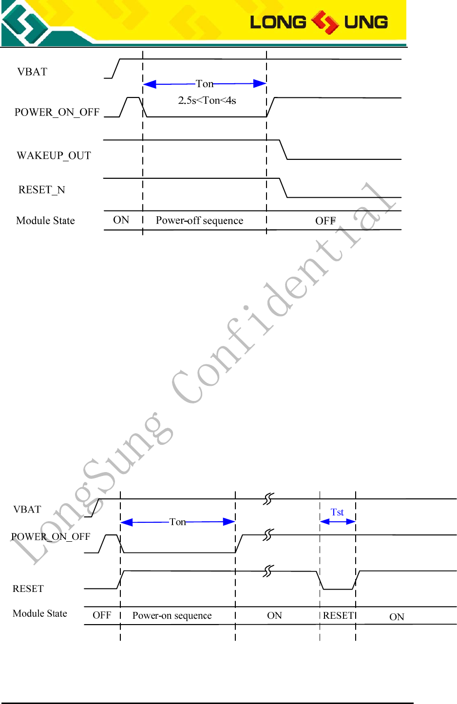
U5501_Hardware_User_Guide_V2.3 Page 27 of 59
Figure10:U5501 power off time sequence
3.2.2.3. Low power to power off
When the power supply of U5501 VBAT is below 3.3V (include VBAT is off), the
module will be power off.
Note: In this case, the module don`t logout from the BS.
3.2.3. Reset time sequence
Control RESET_N (RESET) to set U5501 reset. The RESET_N is active by low
level. The RESET_N signal must be a Tst (100mS) low pulse. Send AT+RESET
can reset the U5501 too.
Figure11:U5501 RESET time sequence
U5501_Hardware_User_Guide_V2.3 Page 28 of 59
3.3. USB interface
3.3.1. USB interface description
U5501 module supports a USB2.0 High-Speed interface. U5501 default PID is
0X9603. When the USB drivers of U5501 are installed, the OS will detect 3
virtual serial ports: Modem port, Diagnostic port and AT port.
Table7:U5501 USB interface
PIN Name I/O PIN No. 描述
USB_DM I/O 85 USB data-
USB_DP I/O 86 USB data+
GND 48~50,52~59,106,108,
110,112,114,116 GND
3.3.2. USB reference circuit
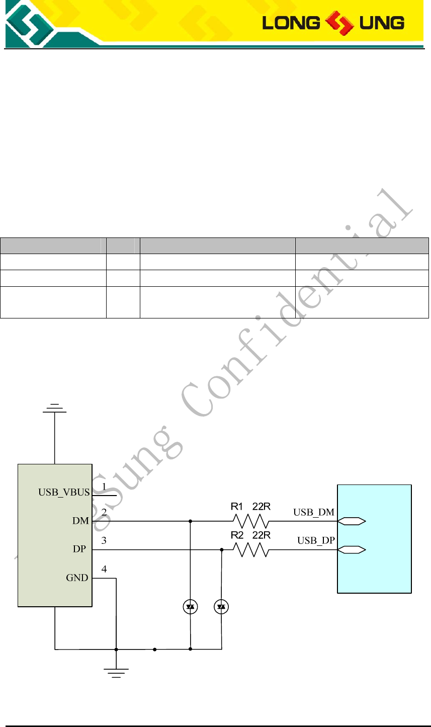
The USB part reference design circuit is as follow
Module
65
USBBF
ESD
ESD
Figure12:U5501 USB reference circuit

U5501_Hardware_User_Guide_V2.3 Page 29 of 59
1) To get the reliable USB power supply, it is recommended to use a 10uF (C1)
filter capacitor and a 33pF (C2) filter capacitor. DC rated voltage of the
capacitors should be above 10V;
2) To reduce the reflection caused by the high frequency alternating signal in
the transmission, it is recommended to add a resistor with value below 10Ω
to the DM and DP in USB interface to ensure correct transmission for USB
data. Just like the resistors R1 and R2;
3) To avoid static electricity in USB interface, it is recommended to use the ESD
protection device. Junction capacitance of the ESD component should be
less than 5pF;
4) To get the reliable USB data transfer, need protect the USB device. Such as
must protect the USB_DP, USB_DM, need 90Ω impedance control, and let
them keep away from the interference signal.
3.3.3. USB driver
U5501 module support many kinds of OS, such as: Windows 2000, Windows XP,
Windows Vista32/64, Windows 7, Windows CE5.0/6.0, Windows Mobile5.0/6.0.
When use these systems, need special drivers for U5501.
For different OS and VID and PID, the drivers are different. If need them, please
contact with FAE of LongSung. The default VID and PID is: VID_1C9E &
PID_9603.
For Linux OS, such as Radhat, Ubuntu and Android, need the OS itself USB
driver usbserial.ko. You need load the driver usbserial.ko and PID, VID to the
system.

U5501_Hardware_User_Guide_V2.3 Page 30 of 59
3.3.3.1. Linux OS load USB driver for U5501
Make sure there is usbserial.ko driver in your Linux system. Linux2.4.X and
Linux2.6.X OS have usbserial.ko, but for some Ubuntu editions must recompile
the kernel to get the usbserial.ko.
The following is in PC Linux2.6.X OS load driver process. (Note: Embed Linux
OS may have some difference)
1) Please insert U5501 to the AP with Linux system by USB. And make sure the
power supply for U5501 is active and steady and can power on U5501;
2) Preparation of lookup USB devices by Linux usbfs filesystem, mount the
USB filesystem, type the command like this:
#mount -t usbfs none /proc/bus/usb
3) Check the status of AP device, in order to make sure AP is ready, we can
type command like this:
#cat /proc/bus/usb/devices
Then we will get the result as the following:
T: Bus=03 Lev=01 Prnt=01 Port=00 Cnt=01 Dev#=9 Spd=12 MxCh= 0
D: Ver= 1.10 Cls=00(>ifc ) Sub=00 Prot=00 MxPS=64 #Cfgs= 1
P: Vendor=1c9e ProdID=9603 Rev= 0.00
S: Manufacturer=Qualcomm, Incorporated
S: Product=Qualcomm CDMA Technologies MSM
C:* #Ifs= 5 Cfg#= 1 Atr=a0 MxPwr=500mA
I:* If#= 0 Alt= 0 #EPs= 3 Cls=ff(vend.) Sub=ff Prot=ff Driver=(none)
E: Ad=81(I) Atr=03(Int.) MxPS= 16 Ivl=128ms
E: Ad=82(I) Atr=02(Bulk) MxPS= 64 Ivl=0ms
E: Ad=02(O) Atr=02(Bulk) MxPS= 64 Ivl=0ms
I:* If#= 1 Alt= 0 #EPs= 2 Cls=ff(vend.) Sub=ff Prot=ff Driver=(none)

U5501_Hardware_User_Guide_V2.3 Page 31 of 59
E: Ad=84(I) Atr=02(Bulk) MxPS= 64 Ivl=0ms
E: Ad=04(O) Atr=02(Bulk) MxPS= 64 Ivl=0ms
I:* If#= 2 Alt= 0 #EPs= 2 Cls=ff(vend.) Sub=ff Prot=ff Driver=(none)
E: Ad=86(I) Atr=02(Bulk) MxPS= 64 Ivl=0ms
E: Ad=06(O) Atr=02(Bulk) MxPS= 64 Ivl=0ms
If the USB device is ready, we can see the red characters listed above. From
it, the vendor ID and product ID is 1c9e and 9603. Like Vendor=1c9e
ProdID=9603 Rev= 0.00.
Also, we can see three serial ports displayed by blue characters. They are
diagnostic port, AT port and modem port (The ports from the top to the
bottom should be like this: DIAG, AT, MODEM).
4) Install USB drivers in AP, type command like this:
#modprobe usbserial vendor=0x1c9e product=0x9603
5) Check the status of device driver, type command like this:
#cat /proc/bus/usb/devices
You my get the result as the following:
T: Bus=03 Lev=01 Prnt=01 Port=00 Cnt=01 Dev#=3 Spd=12 MxCh= 0
D: Ver= 1.10 Cls=00(>ifc ) Sub=00 Prot=00 MxPS=64 #Cfgs=1
P: Vendor=1c9e ProdID=9603 Rev= 0.00
S: Manufacturer=Qualcomm, Incorporated
S: Product=Qualcomm CDMA Technologies MSM
C:* #Ifs= 5 Cfg#= 1 Atr=a0 MxPwr=500mA
I:* If#= 0 Alt= 0 #EPs= 3 Cls=ff(vend.) Sub=ff Prot=ff Driver=usbserial_generic
E: Ad=81(I) Atr=03(Int.) MxPS= 16 Ivl=128ms
E: Ad=82(I) Atr=02(Bulk) MxPS= 64 Ivl=0ms
E: Ad=02(O) Atr=02(Bulk) MxPS= 64 Ivl=0ms
I:* If#= 1 Alt= 0 #EPs= 2 Cls=ff(vend.) Sub=ff Prot=ff Driver=usbserial_generic
E: Ad=84(I) Atr=02(Bulk) MxPS= 64 Ivl=0ms

U5501_Hardware_User_Guide_V2.3 Page 32 of 59
E: Ad=04(O) Atr=02(Bulk) MxPS= 64 Ivl=0ms
I:* If#= 2 Alt= 0 #EPs= 2 Cls=ff(vend.) Sub=ff Prot=ff Driver=usbserial_generic
E: Ad=86(I) Atr=02(Bulk) MxPS= 64 Ivl=0ms
E: Ad=06(O) Atr=02(Bulk) MxPS= 64 Ivl=0ms
If the driver is ready, we can see the usbserial_generic on the right side of
each port.
6) Check the device point in the /dev filesystem:
#cd /dev
# ls ttyUSB*
If the AP driver is OK, there should be ttyUSB0~ ttyUSB2.
3.3.3.2. Linux OS AP use AT to control U5501
1) Please insert the USIM/SIM card into the application terminal, make sure
the USIM/SIM card with Data service already been permitted. Plug the
WCDMA/GSM antenna to RF connector of U5501. Power on the module
U5501, load the USB driver, create USB end ports: ttyUSB0~ ttyUSB2.
2) Run minicom application in Linux OS:
#minicom –s
In the menu of minicom select “Serial port setup”, set “Serial device ” as
/dev/ttyUSB1 (Note: AT(ttyUSB1), Modem(ttyUSB2) can response AT
commands, Diag (ttyUSB0) can not response AT commands); Then
back to the menu of minicom and select “Save setup as df1 ”, save the
configuration, then select “exit ” to exit minicom.
3) Send AT commands by minicom
#minicom
It should prompt as the following:
Welcome to minicom 2.3 OPTIONS: I18n
Compiled on Feb 24 2008, 16:35:15. Port /dev/ttyUSB1

U5501_Hardware_User_Guide_V2.3 Page 33 of 59
Press CTRL-A Z for help on special keys
Input AT command to open the echo of AT:
ATE
IF the system is running normally, it should prompt as the following:
OK
Input AT command to get the version of firmware:
AT+LCTSW
Will get the following response:
SoftwareVersion: LQA0082.2.3_MG24
InnerVersion: LQA0082_240085_6.0.8W1215_EFS1.5
OK
Input AT command to get the strength and BER:
AT+CSQ
Will get the following response:
+CSQ: 20,74
OK
Input AT command to get the status of registration:
AT+CREG?
Will get the following response:
+CREG: 0,1
OK
Input AT command to get the information operator:
AT+COPS?
Will get the following response:
+COPS: 0,0,"CHN-CUGSM",2

U5501_Hardware_User_Guide_V2.3 Page 34 of 59
OK
3.3.3.3. Linux OS AP dial PPP connection
1) Repeat loading USB driver and AT communication with U5501. Make
sure U5501 get the normal registration, and the strength of RF signal
will be stronger than 13 (The first parameter of CSQ).
2) Make sure the Linux OS has pppd application, if it hasn’t pppd
application, please install kppp, you will get pppd in your OS.
3) Create a new file: /etc/ppp/chat/gprs-connect-chat
Then add messages as the following:
TIMEOUT 15
ABORT "DELAYED"
ABORT "BUSY"
ABORT "ERROR"
ABORT "NO DIALTONE"
ABORT "NO CARRIER"
TIMEOUT 40
'' \rAT
OK ATS0=0
OK ATE0V1
OK AT+CGDCONT=1,"IP","3GNET"
OK ATDT*99***1#
CONNECT ''
Note: Different USIM/SIM card which you insert in the
application terminal, AT+CGDCONT=1,"IP","3GNET" will be
different. Please contact the operator to get the APN and replace
the parameter "3GNET".

U5501_Hardware_User_Guide_V2.3 Page 35 of 59
4) Modify the configuration of pppd: /etc/ppp/options
If you find the “auth”, modify it as “#auth”. The result is there aren’t ID
verification.
5) Create a new file: /etc/ppp/peer/gprs
Add messages as the following: (The end port must be ttyUSB2):
# Usage: root>pppd call gprs
/dev/ttyUSB2
9600
crtscts
modem
#noauth
debug
nodetach
#hide-password
usepeerdns
noipdefault
defaultroute
user "3gnet"
0.0.0.0:0.0.0.0
ipcp-accept-local
ipcp-accept-remote
#lcp-echo-failure 12
#lcp-echo-interval 3
#noccp
#novj
#novjccomp
#persist
connect '/usr/sbin/chat -s -v -f /etc/ppp/chat/gprs-connect-chat'

U5501_Hardware_User_Guide_V2.3 Page 36 of 59
6) Connect to the Internet:
#pppd call gprs
# ifconfig
If you get the ppp0 net port means that PPP is successful.
eth0 Link encap:Ethernet HWaddr 00:1D:09:33:A7:E1
inet addr:172.16.180.105 Bcast:172.16.180.255 Mask:255.255.255.0 inet6
addr: fe80::21d:9ff:fe33:a7e1/64 Scope:Link UP BROADCAST RUNNING
MULTICAST MTU:1500 Metric:1 RX packets:39793 errors:0 dropped:0
overruns:0 frame:0 TX packets:17971 errors:0 dropped:0 overruns:0 carrier:0
collisions:0 txqueuelen:1000 RX bytes:3445057 (3.2 MiB) TX bytes:20088925
(19.1 MiB) Interrupt:169 lo Link encap:Local Loopback inet addr:127.0.0.1
Mask:255.0.0.0 inet6 addr: ::1/128 Scope:Host UP LOOPBACK RUNNING
MTU:16436 Metric:1 RX packets:20 errors:0 dropped:0 overruns:0 frame:0 TX
packets:20 errors:0 dropped:0 overruns:0 carrier:0 collisions:0 txqueuelen:0
RX bytes:1160 (1.1 KiB) TX bytes:1160 (1.1 KiB)
ppp0 Link encap:Point-to-Point Protocol inet addr:10.182.207.113
P-t-P:10.64.64.64 Mask:255.255.255.255 UP POINTOPOINT RUNNING NOARP
MULTICAST MTU:1500 Metric:1 RX packets:5 errors:0 dropped:0 overruns:0
frame:0 TX packets:6 errors:0 dropped:0 overruns:0 carrier:0 collisions:0
txqueuelen:3 RX bytes:62 (62.0 b) TX bytes:101 (101.0 b)
7) Testing the Internet
# ping 119.75.217.56
It is the IP address of www.baidu.com. If the ping fails, we need add a
route like this:
#route add default gw 10.64.64.64
Note: 10.64.64.64 is the ISP address as the red character above.
# ping www.baidu.com
If ping www.baidu.com fails, we should add DNS to the /etc/resolv.conf

U5501_Hardware_User_Guide_V2.3 Page 37 of 59
8) Disconnect the internet
# killall pppd
3.4. UART interface
U5501 module provides a UART interface. Which can be used for AT interactive
and data transfer.
3.4.1. UART interface description
Table8:U5501 UART 接口
PIN Name I/O PIN No. 描述
UART_DSR O 73 UART data set ready(2.6V)
UART_RTS O 74 UART ready for receive(2.6V)
UART_DCT O 75 UART data carrier detect(2.6V)
UART_TX O 76 UART transmit data output(2.6V)
UART_RING O 77 UART ring indicator(2.6V)
UART_RX I 78 UART receive data input(2.6V)
UART_DTR I 79 UART data terminal ready(2.6V)
UART_CTS I 80 UART clear to send(2.6V)
GND 48~50,52~59,106,108,
110,112,114,116
地
3.4.2. UART interface reference circuit
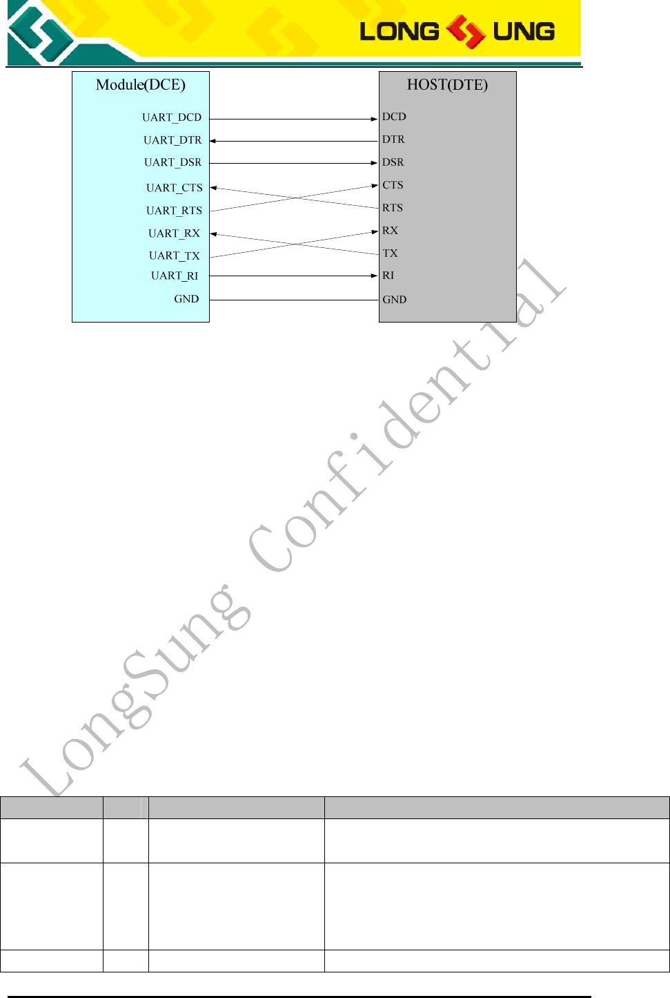
For an application system, U5501 uses as DCE (Data Communication Equipment)
and application terminal uses as DTE (Data terminal equipment). The reference
circuit is as follow:
U5501_Hardware_User_Guide_V2.3 Page 38 of 59
Figure13:U5501 UART connection
3.4.3. UART interface description
1) Full-duplex;
2) 7-bit or 8-bit data;
3) 1-bit or 2-bit stop bit;
4) Odd parity check, even parity check or non-check;
5) Direct memory access(DMA) transmission;
6) Baud rate ranging from 600bps to 230400bps(115200bps by default);
7) Self-adapted baud rate ranging from 1200bps to 115200bps.
3.5. U5501 sleep and wakeup control
In order to describe easily, it is named U5501 as BP and the MCU of application
terminal as AP.
Sleep and wakeup interface is described in the table as follow:
Table9:U5501 sleep and wakeup interface
PIN Name I/O PIN No. 描述
WAKEUP_IN I 11 H: DTE wakeup U5501;
L: DTE set U5501 to sleep mode.
WAKEUP_OUT O 71
H: Module is in wakeup mode and module serial/USB
is available;
L: Module is in sleep mode and serial/USB is not
available.
GND 48~50,52~59,106,108, GND
U5501_Hardware_User_Guide_V2.3 Page 39 of 59
110,112,114,116
3.6. Analog audio interface
U5501 provide 2 channels analog audio interface.
3.6.1. Analog audio interface description
The audio signals are shown in as follow:
Table10 :U5501 analog audio interface description
PIN Name I/O PIN No. 描述
MIC2_P I 38 Positive pole of the input of audio interface 2
MIC2_N I 39 Negative pole of the input of audio interface 2
MIC1_P I 40 Positive pole of the input of audio interface 2
MIC1_N I 41 Negative pole of the input of audio interface 2
EAR_OUT_N O 96 Negative pole of the output of earphone
EAR_OUT_P O 97 Positive pole of the output of earphone
SPKR_OUT_P O 98 Positive pole of the output of speaker
SPKR_OUT_N O 99 Negative pole of the output of speaker
3.6.2. Hands-free channel
The second audio channel can be used for the hands-free without requiring any
audio amplifier. The output pins are configured differently, with a rated output of
500mW into an 8 Ω speaker. Considerable current flows between the audio
output pins and the speaker, and thus wide PCB traces are recommended 20
mils.
Table11 :U5501 second channel audio
PIN Name PIN No. Hands-free Description
SPKR_OUT_P 98 SPK_P Loudspeaker output differential signal +
SPKR_OUT_N 99 SPK_N Loudspeaker output differential signal -
MIC2_P 38 MIC_P Audio input channel 2 differential signal +
MIC2_N 39 MIC_N Audio input channel 2 differential signal -
3.6.3. Handset channel
The first audio channel can be used for the handset without requiring any audio
amplifier. The output power for the differential ear output is typically 350 mW
U5501_Hardware_User_Guide_V2.3 Page 40 of 59
for a full-scale +3 dBm sine wave into a 32-ohm speaker.
Table12 :U5501 first channel audio
PIN Name PIN No. Handset Description
EAR_OUT_N 96 EAR_N Audio output channel 1 differential signal -
EAR_OUT_P 97 EAR_P Audio output channel 1 differential signal +
MIC1_P 40 MIC_P Audio input channel 1 differential signal +
MIC1_N 41 MIC_N Audio input channel 1 differential signal -
3.6.4. Analog audio reference circuit
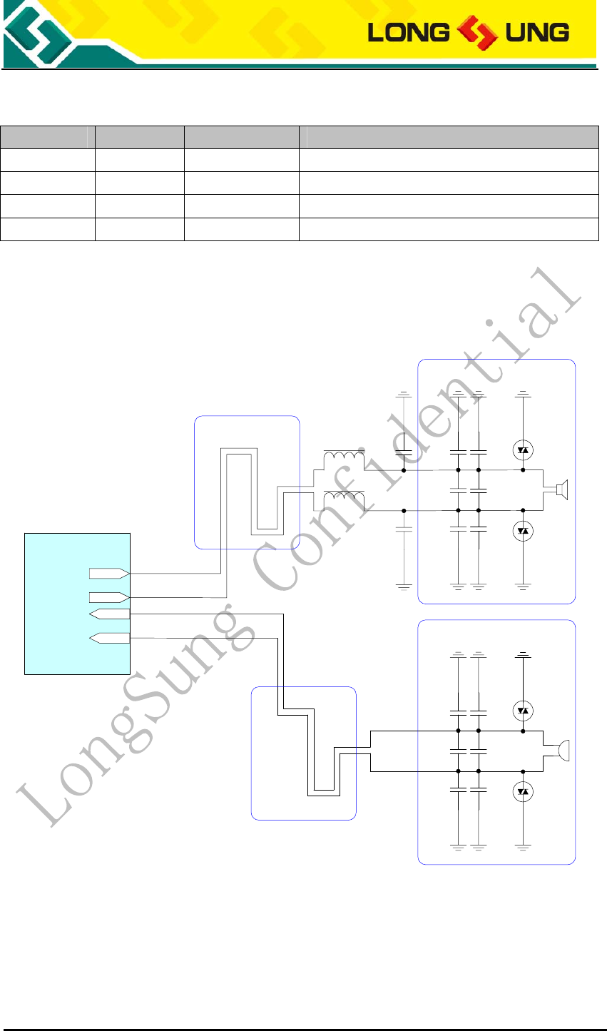
The U5501 analog audio reference circuit is shown as follow:
10pF 33pF
ESD
10pF 33pF
10pF 33pF ESD
Differential Layout
Close to Speaker
10pF 33pF
ESD
10pF 33pF
10pF 33pF ESD
Differential Layout
Close to MIC
MIC1_P/MIC2_P
MIC1_N/MIC2_N
EAR_P/SPK_P
EAR_N/SPK_N
Module
BEAD
BEAD
1nF
1nF
Figure14:U5501 analog audio reference circuit
1) The audio output signals, a pair of differential signals, output to two
speakers. The output signals are not real stereo signals which are different

U5501_Hardware_User_Guide_V2.3 Page 41 of 59
from traditional stereo sound.
2) It is recommended to use the filter capacitor or filter circuit to reduce inter
frequency interference and improve audio quality. Just like what is shown in
the figure above.
3) To avoid static electricity, it is recommended to use the ESD protection
device.
4) It requires connecting audio analog signal ground with the general digital
circuit ground, magnetic bead or zero ohm resistance can be used.
5) IF use an audio amplifier for speaker, optional EMI filtering is shown at
Fogure14, these components (two ferrite beads and two capacitors) can be
added to reduce electromagnetic interference. If used, they should be
located near the EAR_P and EAR_N.
6) Considerable current between the audio output pins and the speaker, the
width of PCB traces are recommended 20mils.
3.7. PCM interface
U5501 module provides a PCM interface. The PCM include 4 pin digital signals.
Use PCM interface can support communication between U5501 and external
CODEC.
PCM TX data will be routed from the external codec MIC through the DSP encode
path in the U5501 module. PCM RX data will be routed through the DSP decode
path to the external codec speaker.
The base band of U5501 can be used in two modes:
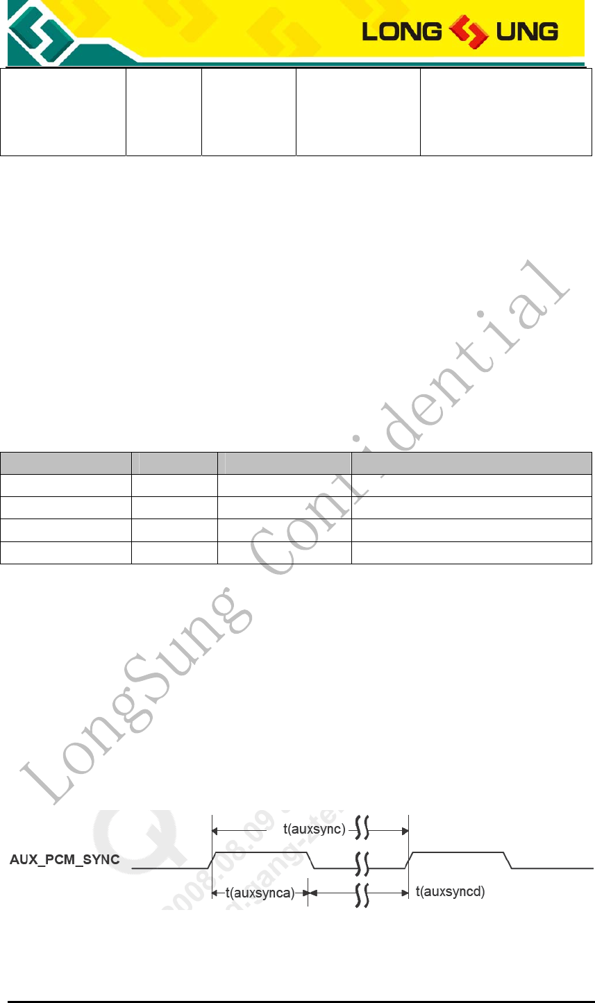
1) Auxiliary PCM, the auxiliary PCM that runs at 128 kHz and uses a 62.5 μs
sync pulse (half a time frame).
2) Primary PCM, the primary PCM that runs at 2.048 MHz and uses 488 ns sync
pulse (one 2.048 MHz clock tick).
Table13 :Auxiliary PCM and Primary PCM configuration
Configuration SYNC CLK Clock source Format
Auxiliary 8KHz 128KHz Master 8Bits μ-law,
U5501_Hardware_User_Guide_V2.3 Page 42 of 59
Primary 8KHz 2.048MHz Master/Slave
8Bits A-law,
16Bits Linear (13 bits
are valid, the others
are blank)
The default configuration of U5501 is Primary PCM, and can use AT command to
select Master Mode or Slave Mode.
In Slave mode, the external codec drives the clock and sync signals that are
sent to the U5501 module.
U5501 module supports 3 PCM formats: 8Bits μ-law, 8Bits A-law, 16Bits
(Linear).
3.7.1. PCM interface description
Table14 :U5501 PCM interface
PIN Name I/O PIN No. Description
PCM_SYNC O 5 PCM Synchronous Signal
PCM_CLK I 8 PCM CLK
PCM_DIN I 6 PCM Input
PCM_DOUT O 7 PCM Output
3.7.2. Auxiliary PCM
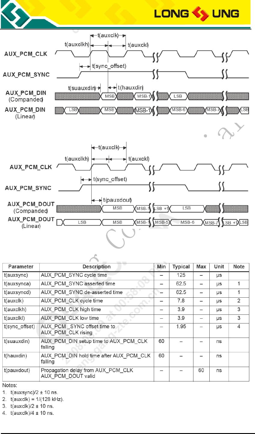
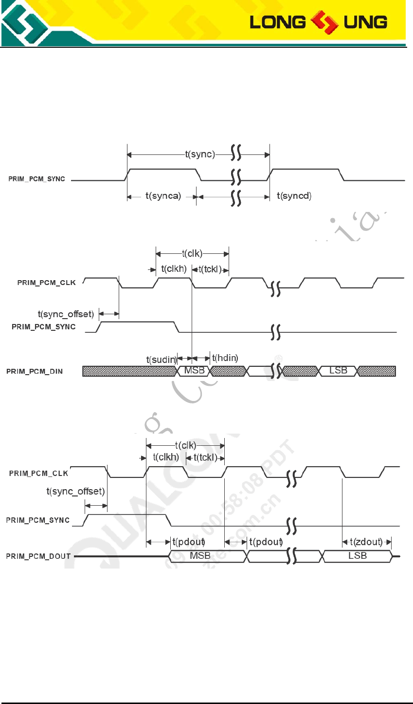
The Auxiliary PCM interface enables communication with an external codec to
support hands-free applications. The auxiliary codec port operates with
standard long-sync time sequence and a 128 kHz clock. The AUX_PCM_SYNC
runs at 8 kHz with a 50% duty cycle. Most μ-law and A-law codecs support the
128 kHz AUX_PCM_CLK bit clock.
Figure15:AUX_PCM_SYNC time sequence
U5501_Hardware_User_Guide_V2.3 Page 43 of 59
Figure16:AUX_PCM_CODEC to U5501 time sequence
Figure17:U5501 to AUX_PCM_CODEC time sequence
Table15 :AUX_CODEC time sequence parameters
U5501_Hardware_User_Guide_V2.3 Page 44 of 59
3.7.3. Primary PCM
U5501 module firmware default configuration is Primary PCM. PRIM_PCM_CLK
is 2.048 MHz clock, PRIM_PCM_SYNC is 8 kHz (488nS), and μ-law PCM format.
Figure18:PRIM_PCM_SYNC time sequence
Figure19:PRIM_PCM_CODEC to U5501 time sequence
Figure20:U5501 to PRIM_PCM_CODEC time sequence
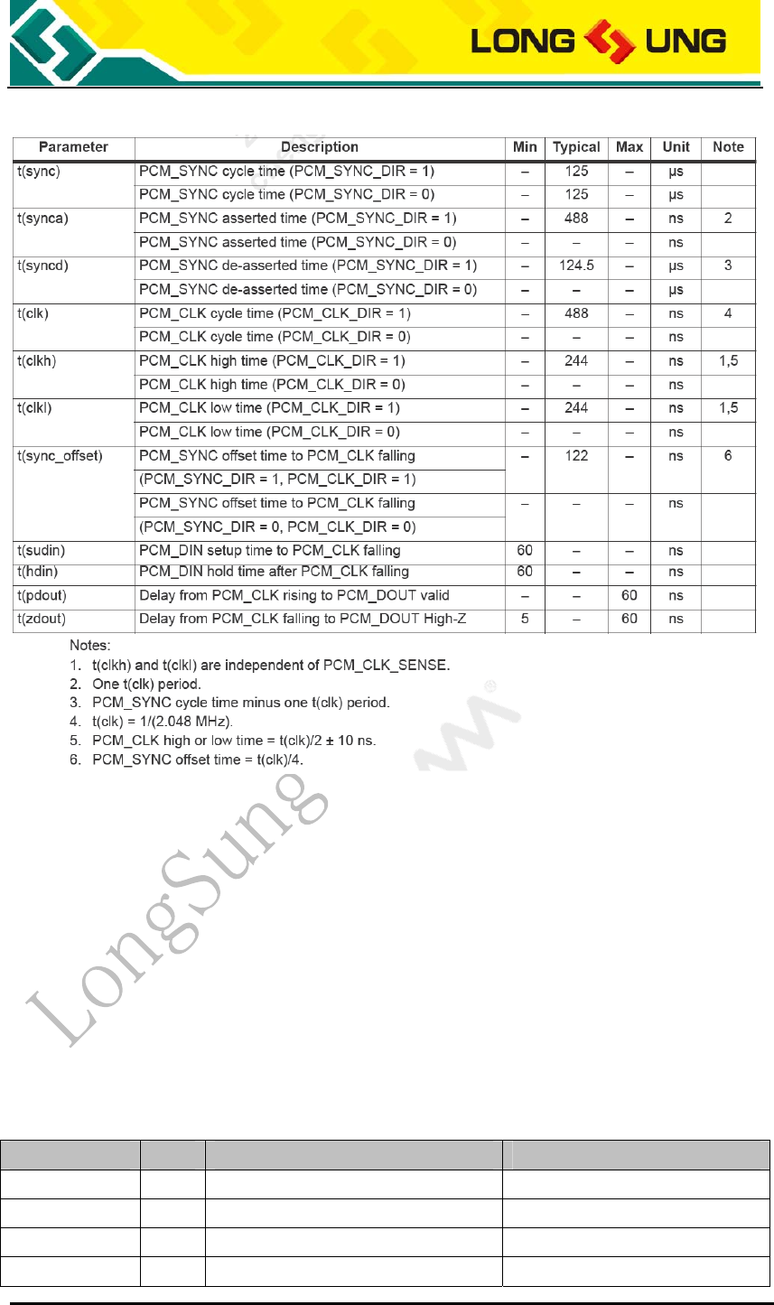
U5501_Hardware_User_Guide_V2.3 Page 45 of 59
Table16 :PRIM_CODEC time sequence parameters
3.8. USIM/SIM interface
U5501 module supports HSPA/UTMS mode USIM card and GSM/GPRS/EDGE
mode SIM card.
3.8.1. USIM/SIM interface description
U5501 module supports 1.8/3.0V USIM/SIM card.
Table17 :U5501 USIM/SIM 接口
PIN Name I/O PIN No. Description
SIM_DATA I/O 89 USIM/SIM DATA
SIM_CLK O 90 Clock Signal
SIM_RESET O 88 RESET Signal
SIM_VCC O 34 USIM/SIM Power

U5501_Hardware_User_Guide_V2.3 Page 46 of 59
SIM_DET I 70 USIM/SIM detect
GND
48~50,52~59,106,108,
110,112,114,116
地
3.8.2. USIM/SIM interface reference circuit
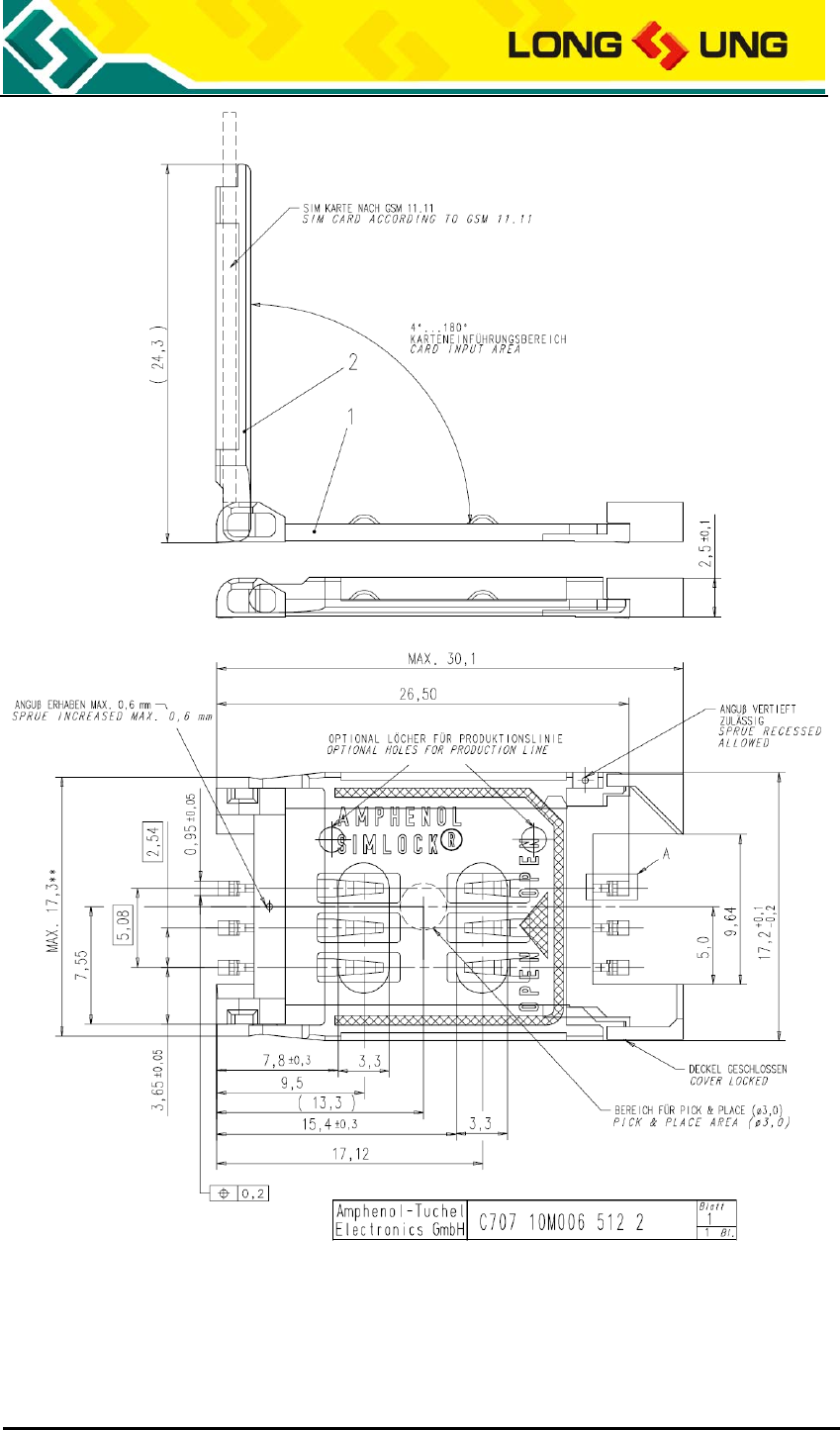
For 6-pin USIM/SIM card, we recommend to use the Amphenol C707 10M006
512 2 SIM Holder. For more information, you can visit the Amphenlo company
web: http://www.amphenol.com/
The SPEC of C707 10M006 512 2 SIM Holder is as follow.
U5501_Hardware_User_Guide_V2.3 Page 47 of 59
Figure21:The SPEC of C707 10M006 512 2 SIM Holder
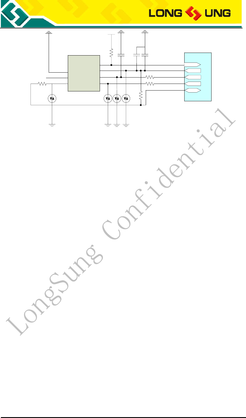
USIM/SIM interface reference design circuit as follow.
U5501_Hardware_User_Guide_V2.3 Page 48 of 59
Module
22
22
SIM_VCC
SIM_RESET
SIM_CLK
SIM_DATA
33pF
100nF
VCC
RST
CLK
GND
VPP
IO
1
2
3
6
5
4
22
15K
33pF
ESD
ESD
ESD
ESD
SIM_DET
DET 7
10K
3.3V
Figure22:U5501 USIM/SIM interface reference circuit
1) The USIM_DATA line of USIM is connected to USIM_VCC by a pull-up
resistor with reference value 10KΩ;
2) To avoid the instantaneous voltage overflowing, the resistor with reference
value 22Ω can be used for the USIM_DATA, USIM_CLK and USIM_RESET
line;
3) To avoid the static electricity in USIM socket, it is recommended to use the
ESD protection device for the USIM_DATA, USIM_CLK and USIM_VCC line;
4) To get more flat USIM power supply, it is recommended to use the filter
capacitors, and reference value 33pF and 100nF;
5) To eliminate the peak interference and high frequency interference signal on
USIM_RESET line, the filter capacities can be placed in USIM_RESET line,
the reference value is 33pF;
6) SIM_DET is the USIM/SIM insert or remove detector.
3.9. Status indicator interface
The U5501 provide 2 status indicators, which are PIN91 and PIN101.
3.9.1. Status indicator description
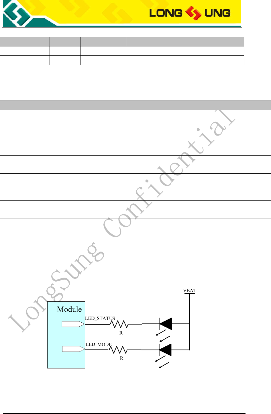
The U5501 status indicator is decribed as follow.
U5501_Hardware_User_Guide_V2.3 Page 49 of 59
Table18 :U5501 status indicator description
PIN Name I/O PIN No. Description
LED_STATUS O 91 Status indicator
LED_MODE O 101 Status indicator
Status indicator is described as follow.
Table19 :U5501 status indicator description
Status LED_STATUS LED_MODE
1 Registered in 3G
network
The indicator blinks once
each time(100ms
On/2900ms Off)
Light off
2 3G network data
transferring Light on Light off
3 Download
firmware Light off The indicator blinks fast (100ms
On/100ms Off)
4 Searching
network Light off
The indicator blinks twice each time
(100ms On/100ms Off/100ms
On/2700ms Off)
5 Registered in 2G
network Light off The indicator blinks once each time
(100ms On/2900ms Off)
6 2G network data
transferring Light off Light on
3.9.2. Status indicator reference circuit
The status indicator reference circuit is shown as follow:
Figure23:U5501 status indicator reference circuit
IF *R+VF = VBAT
VF: LED Forward Voltage
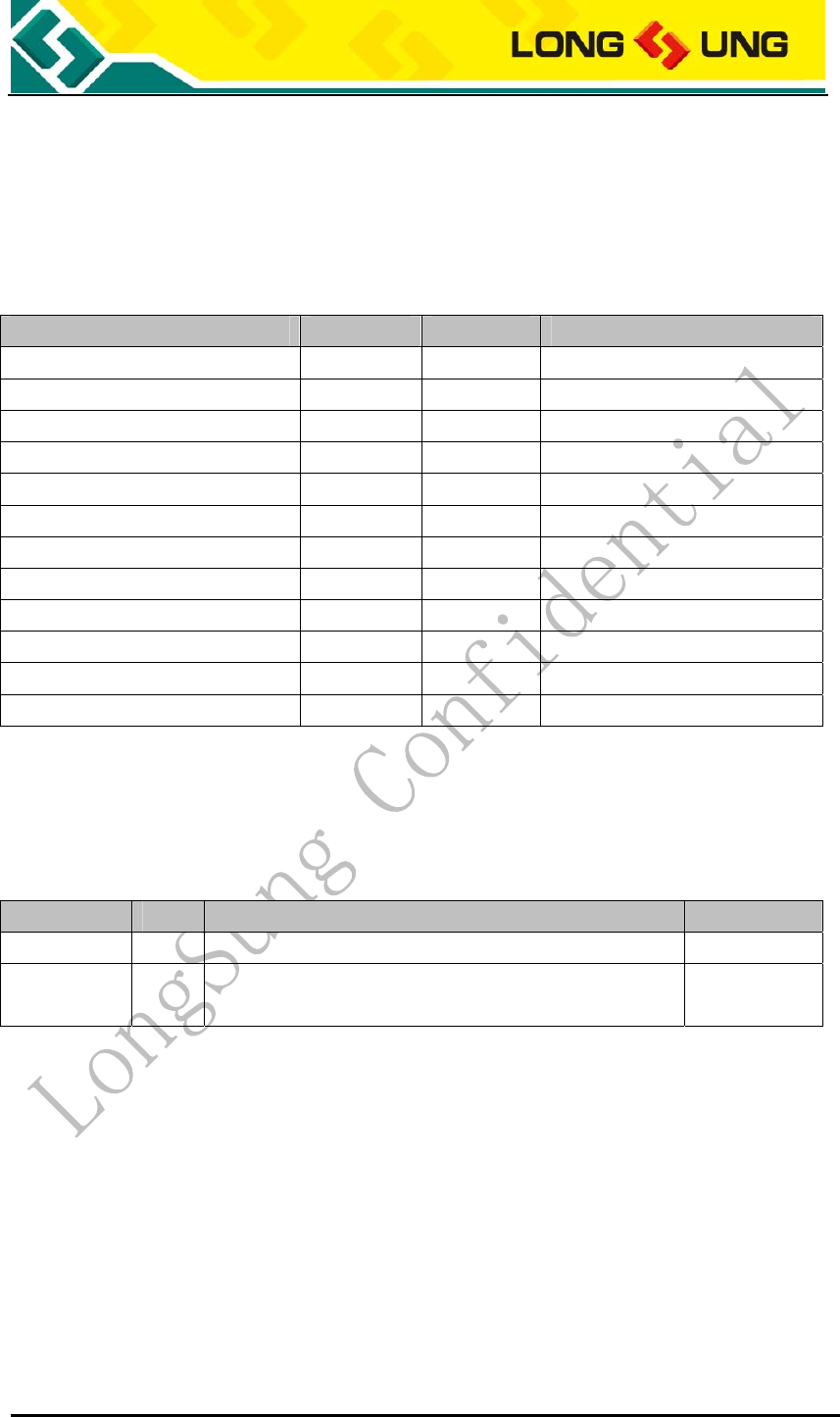
U5501_Hardware_User_Guide_V2.3 Page 50 of 59
IF: LED Forward current
3.10. GPIO
U5501 provide several GPIOs.
Table20 :U5501 GPIOs
PIN Name I/O PIN NO. Description
GPIO_2.6V I/O 15 2.6V voltage level
GPIO_1.8V I/O 28 1.8V voltage level
GPIO_1.8V I/O 29 1.8V voltage level
GPIO_2.6V I/O 43 2.6V voltage level
GPIO_2.6V I/O 44 2.6V voltage level
GPIO_2.6V I/O 45 2.6V voltage level
GPIO_2.6V I/O 46 2.6V voltage level
GPIO_2.6V I/O 51 2.6V voltage level
GPIO_2.6V I/O 55 2.6V voltage level
GPIO_2.6V I/O 105 2.6V voltage level
GPIO_2.6V I/O 109 2.6V voltage level
GPIO_2.6V I/O 113 2.6V voltage level
3.11. Antenna interface
PIN107 is the antenna pad.
Table21 :U5501 antenna interface
PIN Name I/O PIN No. Description
ANT 107 Antenna
GND
48~50,52~59,106,108,
110,112,114,116 GND
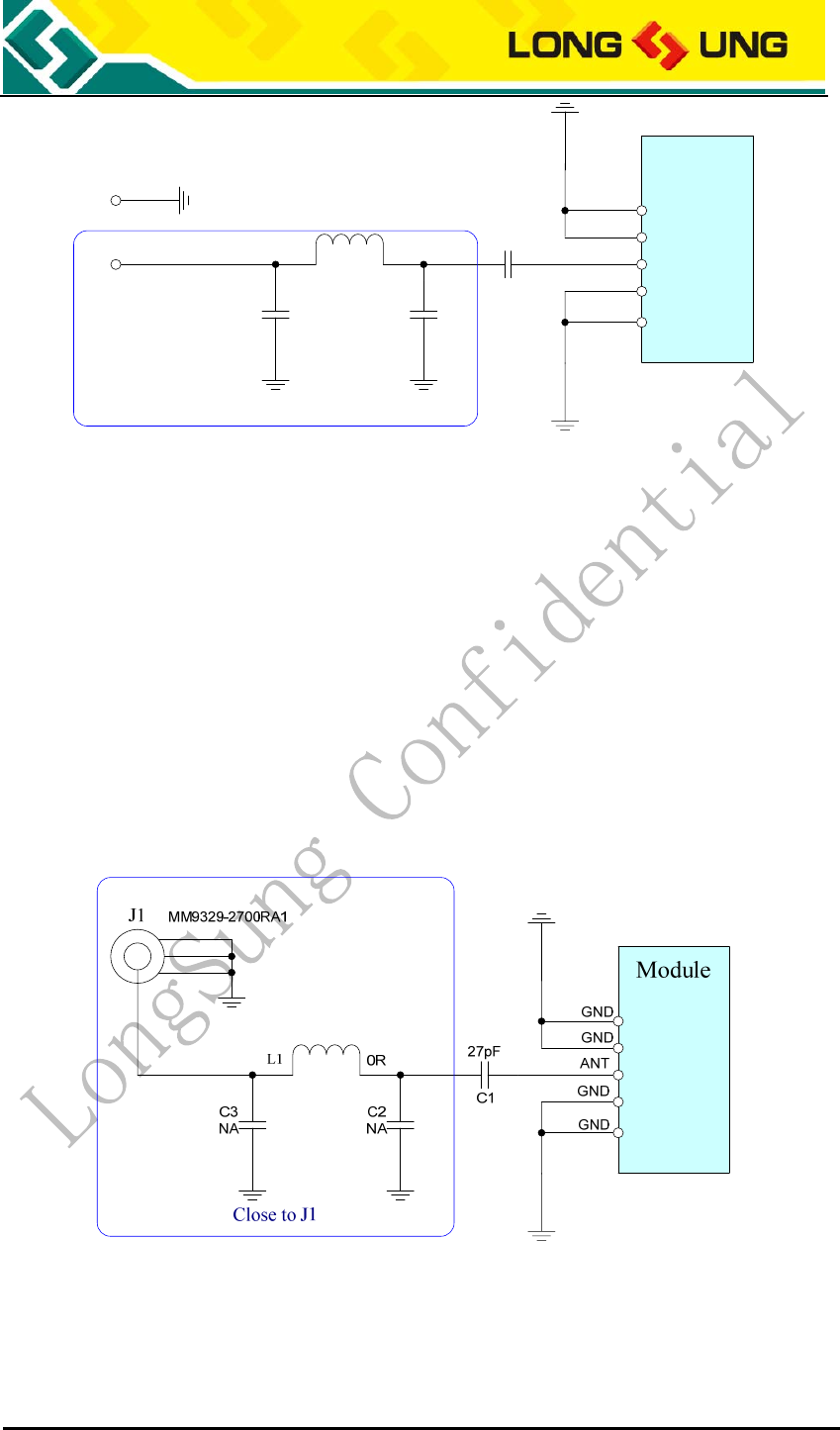
There are two types antenna reference design with the U5501, one is the solder
antenna, the other is use the antenna connector. We recommend to layout with
microstrip line in both of the two types.
3.11.1. Solder antenna
The reference circuit of solder antenna is shown as follow:
U5501_Hardware_User_Guide_V2.3 Page 51 of 59
Module
GND
GND
ANT
GND
27pF
GND
L1
C2
NA
C1
0R
C3
NA
2.0×2.0mm
3.0×3.0mm
TP1
TP2
Close to TP1
Figure24:U5501 solder antenna reference circuit
The matters need attention about the U5501 solder antenna are as follow:
1) PI type matching filter(L1, C2, C3) must close to the TP1, and separate the
GND pad(TP2) from the TP1 0.7mm at least;
2) Control the microstrip line impedance to 50ohm;
3) Keepout: We recommend the trace width 1.2mm in top layer, and separate
the other trace from 1.2mm, there need not keepout in bottom layer.
3.11.2. RF connector
The reference circuit of the U5501 use the RF connector is as follow:
Figure25:U5501 RF connector reference circuit
We recommend the antenna connector(J1) type is MM9329-2700RA1 which
provided by MURATA.
The matters need attention of the U5501 antenna connector are as follow:

U5501_Hardware_User_Guide_V2.3 Page 52 of 59
1) PI type matching filter(L1, C2, C3) must close to the TP1, and separate the
GND pad(TP2) from the TP1 0.7mm at least;
2) Control the microstrip line impedance to 50ohm;
3) Keepout: We recommend the trace width 1.2mm in top layer, and separate
the other trace from 1.2mm, there need not keepout in bottom layer.
3.11.2.1. RF cable
When you use RF Connector, please select the RF cable carefully; it is required
to use RF cable of which the insertion loss should comply with:
z GSM900/GSM850<1dB
z DCS1800/PCS1900<1.5dB
z WCDMA2100<1.5dB
z WCDMA900<1dB
We recommend use the MXTK88TK200 which provided by MURATA.
3.11.3. U5501 RF output power
The RF output power of U5501 is shown as follow:
Table22 :U5501 RF output power
Band Max Min
GSM850 33dBm ± 1dB 5dBm ± 5dB
E-GSM900 33dBm ± 1dB 5dBm ± 5dB
DCS1800 29dBm ± 1dB 0dBm ± 5dB
PCS1900 29dBm ± 1dB 0dBm ± 5dB
WCDMA2100 24dBm +1/-3dB -56dBm ± 9dB
WCDMA900 24dBm +1/-3dB -56dBm ± 9dB
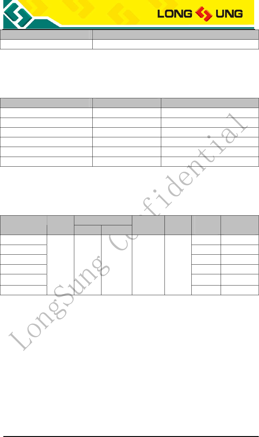
3.11.4. U5501 RF receiver sensitivity
Table23 :U5501 RF receiver sensitivity
Band Receive sensitivity
GSM850 <-106dBm
E-GSM900 <-106dBm
DCS1800 <-106dBm
PCS1900 <-106dBm
WCDMA2100 <-108dBm
U5501_Hardware_User_Guide_V2.3 Page 53 of 59
Band Receive sensitivity
WCDMA900 <-106dBm
3.11.5. U5501 operating frequencies
Table24 :U5501 operating frequencies
Band Receive Transmit
GSM850 869~894MHz 824~849MHz
E-GSM900 925~960MHz 880~915MHz
DCS1800 1805~1880MHz 1710~1785MHz
PCS1900 1930~1990MHz 1850~1910MHz
WCDMA2100 2110~2170MHz 1920~1980MHz
WCDMA900 880~915MHz 925~960MHz
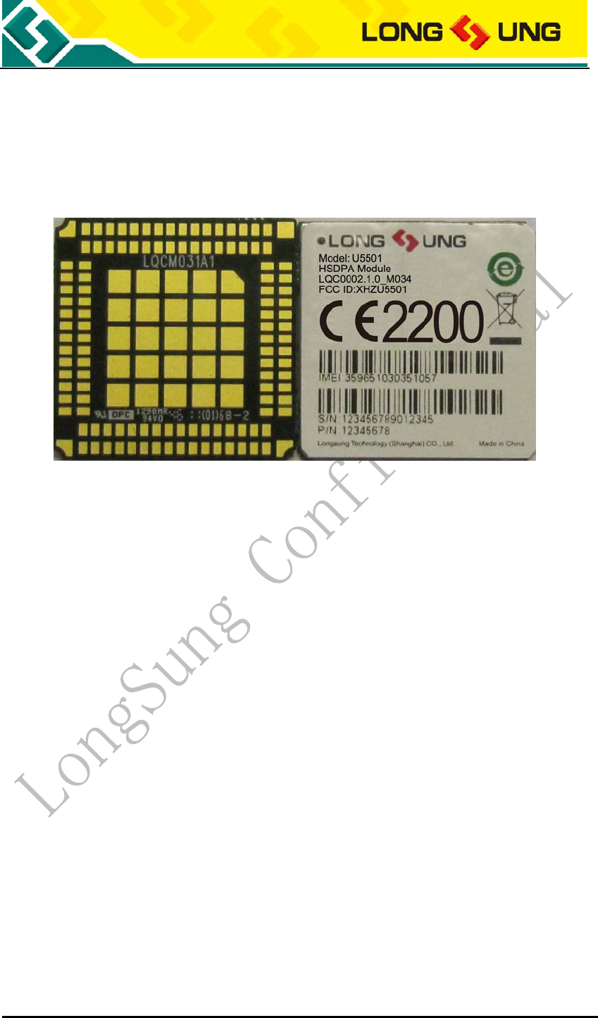
3.11.6. Antenna parameters requirement
Table25 :U5501 antenna parameters requirement
Gain
Band VSWR Peak Avg. Efficiency
SAR TRP
(dBm)
TIS
(dBm)
GSM850 28 <-102
EGSM900 28 <-102
DCS1800 25 <-102
PCS1900 25 <-102
WCDMA900 18 <-102
WCDMA2100
<2.5:1 >0dBi >-4dBi >40% <1.6
W/Kg
18 <-104
U5501_Hardware_User_Guide_V2.3 Page 54 of 59
4. Mechanics
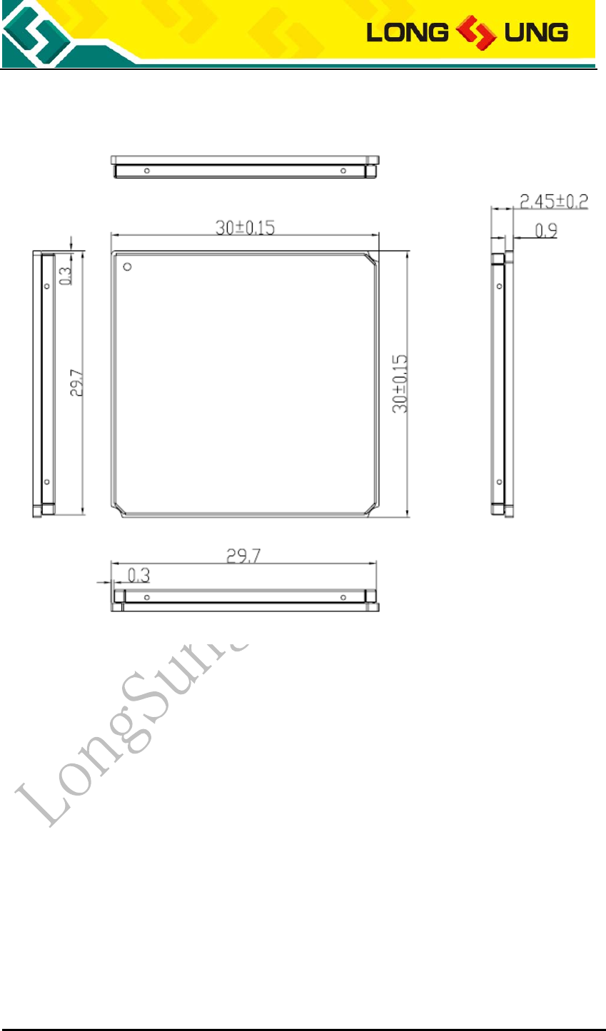
4.1. The view of U5501
Figure26:The view of U5501
4.2. 3D stack
If you need the 3D stack of U5501, please contact us to obtain it.
U5501_Hardware_User_Guide_V2.3 Page 55 of 59
4.3. 2D mechanical dimensions
Figure27:U5501 2D mechanical dimensions
4.4. Application side library of U5501
The library which includes schematic decal and PCB decal. Please contact us to
obtain them.
U5501_Hardware_User_Guide_V2.3 Page 56 of 59
5. Power consumption
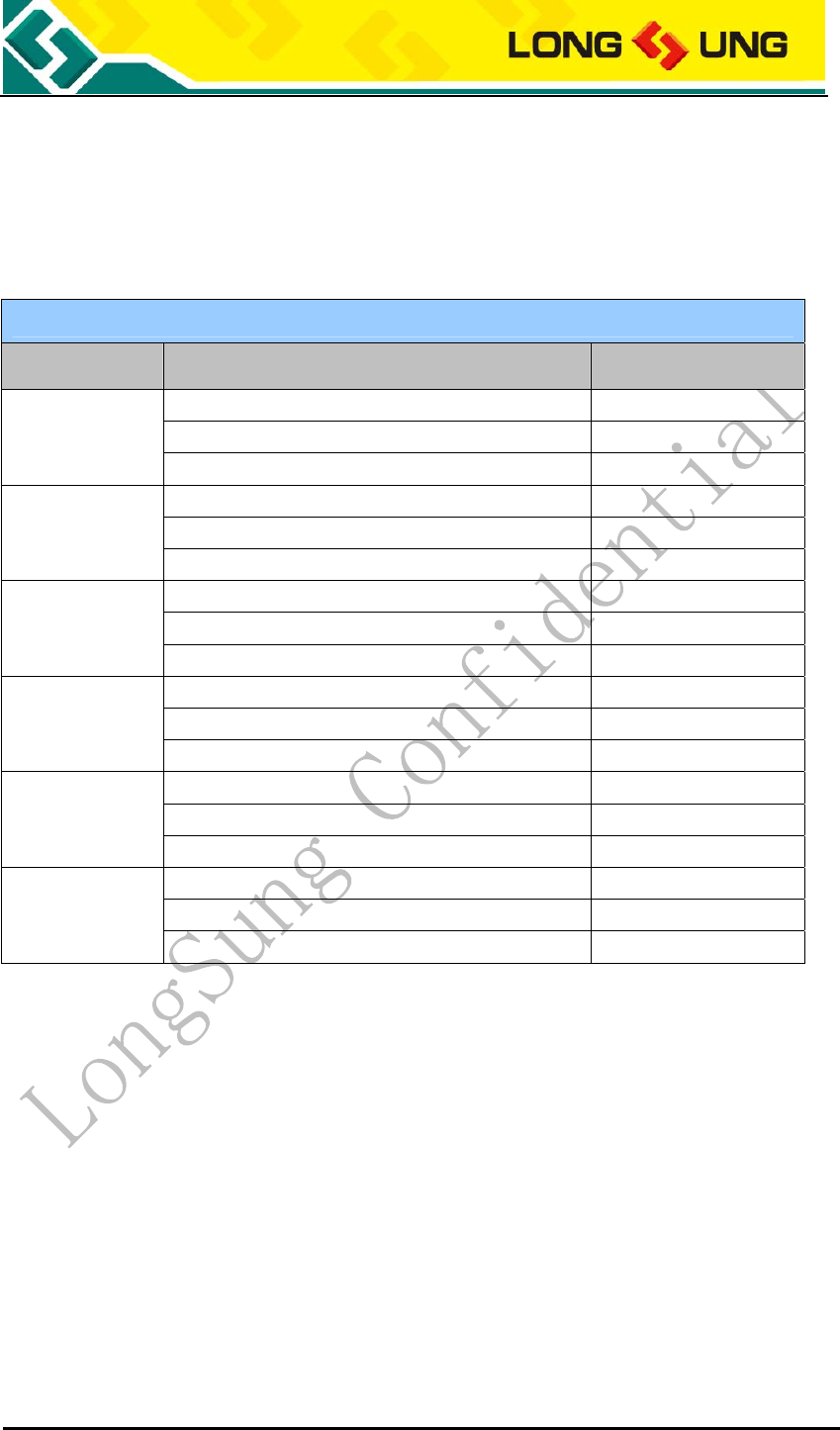
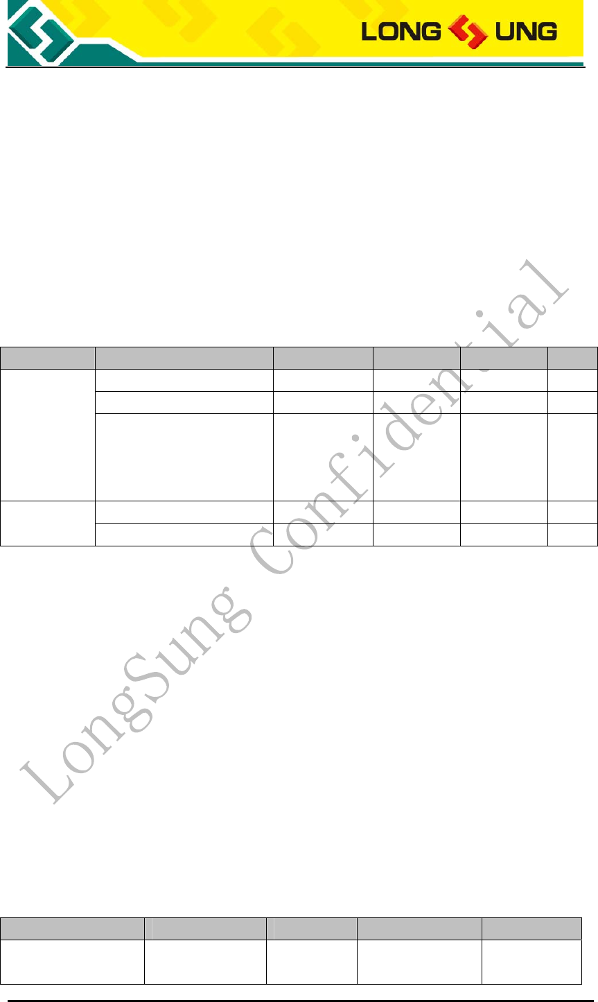
U5501 current consumption (VBAT Power supply: DC3.8V) is shown as follow.
Table26 :U5501 max current consumption in some mode
Sleep 模式状态下耗流
工作频段 配置 平均值(mA)
2 3.2
5 2.1
GSM850
9 1.5
2 3.1
5 1.9
GSM900
9 1.5
2 3.1
5 1.8
DCS1800
9 1.5
2 2.9
5 2
PCS1900
9 1.4
6 3.9
7 2.4
W2100
9 0.8
6 3.9
7 2.7
W900
9 0.8
U5501_Hardware_User_Guide_V2.3 Page 57 of 59
6. Electrical characteristics
6.1. Absolute maximum power ratings
Absolute maximum power ratings for power supply and the voltage on digital
and analog pins of U5501 module are listed as follow. Out of the range, the
module should be damaged.
Table27 :Absolute maximum power ratings
Parameter Description Min Typ Max Unit
U5501 power supply -0.5 3.8 4.2 V
RMS average current 0 0.9 A
VBAT Voltage drop during
transmit burst, IVBAT peak
current may up to 2A (Per
4.6ms)
400 mV
Digital IO voltage -0.3 2.6 3.0 V
GPIO Voltage in power off mode
-0.25 0.25 V
6.2. Operating temperatures
U5501 module can normal operate in the environment temperature in
-20~+65℃.
If you will use it in the environment which out of the range, we recommend
customer has some method to control the temperature around U5501 module.
In the restricted operation temperature, some RF parameter may out of the
3GPP RF standard. The module can work, such as voice, SMS, data.
In the storage temperature, the module may be not able to work, just for
storage. The temperature out of the range, the U5501 module should be
damaged.
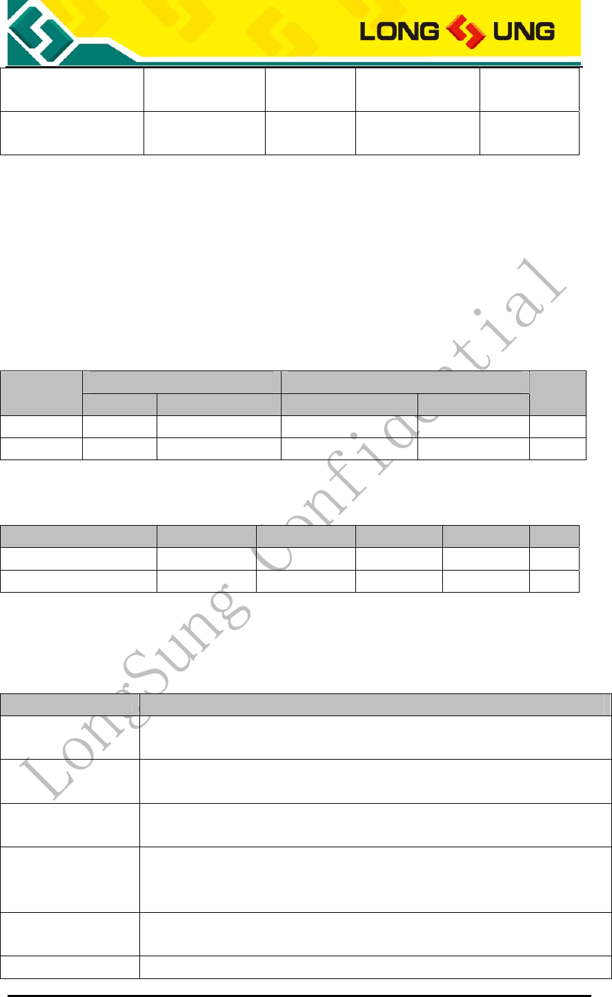
Table28 :U5501 module operating temperature
Temperature Min Typ Max Unit
Normal operation
temperature
-20 25 65 ℃
U5501_Hardware_User_Guide_V2.3 Page 58 of 59
Restricted operation
temperature
-30 ~ -20 65 ~ 75 ℃
Storage
temperature
-40 85 ℃
6.3. Interface operating status
VL:logistic low level;
VH:logistic high level.
Table29 :Digital Signal DC Characteristics
VL VH
Signal Min Max Min Max Unit
Input -0.3 0.3*Vpin_min 0.3*Vpin_max Vpin_max V
Output GND 0.2 Vpin_min-0.2 Vpin V
Note:Vpin_min=2.25V, Vpin_max=3.0V (Vpin is the digital interface high level,Vpin=2.6V)
Table30 :U5501 power supply range
Parameter I/O Min Typ Max Unit
VBAT I 3.3 3.8 4.2 V
SIM_VCC O 1.7/2.75 1.8/2.85 1.9/2.95 V
6.4. Reliability
Table31 :Requirements on the environment reliability
Test case Test requirement
Low temperature
Storage test -40 ±3℃℃, power off mode storage 24 hours
High temperature
Storage test +85 ±3℃℃, power off mode storage 24 hours
Tem pe ra tur e
change test
In power off mode, between -40℃ and +85℃, stay 0.5h, change time
<3min, total 24 times
High temperature
high humidity test
Tem pe ra tur e: + 85 ±3℃℃
Humidity: 90~95%RH
Power off mode storage 24 hours
Low temperature
operating -20 ±3℃℃, keep operating for 24 hours
High temperature +65 ±3℃℃, keep operating for 24 hours

U5501_Hardware_User_Guide_V2.3 Page 59 of 59
Test case Test requirement
operating
Vibration test
Vibration test requirement:
Frequency Random Vibration ASD
5~20Hz 0.96m2/s3
20~500Hz 0.96m2/s3(20Hz), else -3dB/times frequency
Connector Life Test
Board-to-board connector plug 50 times; RF connector plug 30 times
ESD test
1, When module in voice mode, discharge antenna port, VBAT PAD and
GND, ESD must meet the following targets:
1) Contact discharge pass: ±2KV、±4KV test class
2) Air discharge pass: ±2KV、±4KV、±8KV test class
2, When module in voice mode, discharge SIM card hold of EVB, ESD must
meet the following targets:
1) Contact discharge pass: ±2KV test class
2) Air discharge pass: ±2KV、±4KV test class
6.5. Electrostatic discharge
U5501 module is a consumptive product. Although the module has some ESD
protect function, we recommend in application need more ESD protect means to
avoid the static electricity from the application environment, please reference to
the interface reference design circuit.
In order to improve the antistatic performance of the system, we recommend
customer is advised of the following main board: layout an exposed copper
under the module U5501, U5501 shield frame solder feet welded to the
customer board. The solder feet, copper, solder feet and GND are connected.
The ESD capacity of U5501 is listed as follow.
Table32 :The ESD endure status measured table
(Temperature: 25℃, Humidity: 45%)
Part Air discharge Contact discharge
VBAT,GND ±8KV ±4KV
Antenna port ±8KV ±4KV
Other port ±4KV ±2KV