Longcheer Technology A8000 GSM/GPRS module User Manual

Shanghai Longcheer Technology Co., Ltd. GSM/GPRS module
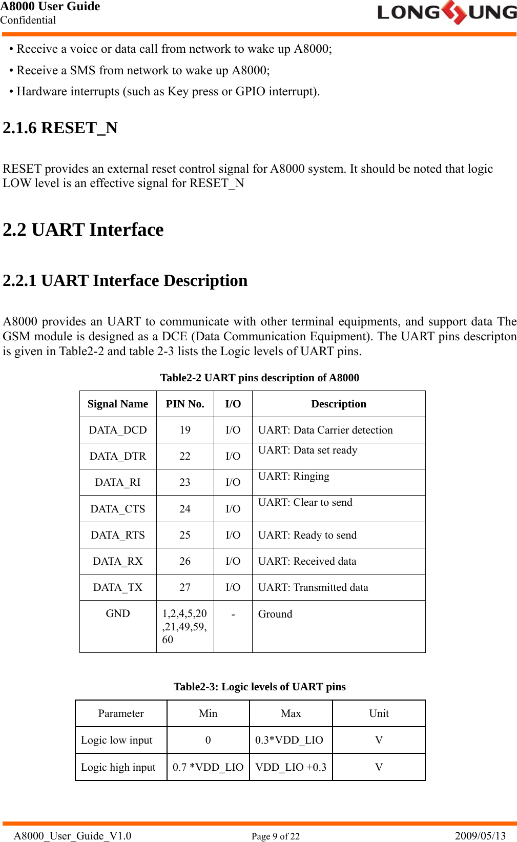
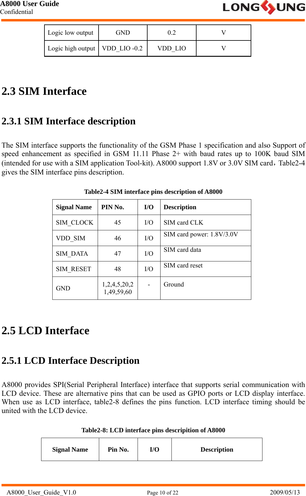
user manual

A8000 User Guide Confidential   A8000_User_Guide_V1.0                      Page1of 22                              7/21/2009    Document Name: A8000 User Guide Version: 1.0 Date: May 13th, 2009 DocId: A8000_User_Guide_V1.0 Status: Confidential / Released  LONGSUNG GSM MUDLE A8000 user guide describes interfaces, function and application, which is provided to LONGSUNG’s customers for testing, evaluation, integration and information. LONGSUNG reserves the right to make changes without further notice to any products herein. LONGSUNG makes no warranty, representation or guarantee regarding the suitability of its products for any particular purpose, nor does LONGSUNG assume any liability arising out of the application or use of any product or circuit, and specifically disclaims any and all liability, including without limitation consequential or incidental damages. LONGSUNG does not convey any license under its patent rights nor the rights of others. COPY RIGHT The document contains LONGSUNG Proprietary Information; therefore, NOT to be used, copied, reproduced in whole or in part, nor its contents revealed in any manner to others without the express written permission of LONGSUNG Technology. Copyright © LONGSUNG 2009
A8000 User Guide Confidential   A8000_User_Guide_V1.0                      Page 2 of 22                            2009/05/13 VERSION HISTORY  Version  Author  Date  Chapter  What is new V1.0 Liu Zhongrong 2009-5-13   Create
A8000 User Guide Confidential   A8000_User_Guide_V1.0                      Page 3 of 22                            2009/05/13 CAUTION: A8000 module is an ESD (electrostatic discharge) sensitive device. Electrostatic charges as high as 1 K Volts readily accumulate on the human body and test equipment and can discharge without detection. Permanent damage may occur on devices subjected to high-energy electrostatic discharges. Therefore, proper ESD precautions are recommended to avoid performance degradation or loss of functionality.
A8000 User Guide Confidential   A8000_User_Guide_V1.0                      Page 4 of 22                            2009/05/13 Contents  1.Introduction................................................................................................................................5 1.1 Overview............................................................................................................................................... 5 1.2 A8000 Key Features........................................................................................................................... 5 1.3 Operating Modes................................................................................................................................6 2.1 Power Supply ...................................................................................................................................... 7 2.1.1 Power Supply Pads on A8000 ..................................................................................................................... 7 2.1.2 Turn On / Off A8000....................................................................................................................................... 8 2.1.2.1 Turn On A8000........................................................................................................................................ 8 2.1.2.2 Turn Off A8000........................................................................................................................................ 8 2.1.3 Power Saving ................................................................................................................................................. 8 2.1.3.1 Sleep Mode............................................................................................................................................. 8 2.1.3.2 Wake Up A8000 From SLEEP Mode................................................................................................... 8 2.1.6 RESET_N ....................................................................................................................................................... 9 2.2 UART Interface.................................................................................................................................... 9 2.2.1 UART Interface Description.......................................................................................................................... 9 2.3 SIM Interface...................................................................................................................................... 10 2.3.1 SIM Interface description............................................................................................................................ 10 2.5 LCD Interface..................................................................................................................................... 10 2.5.1 LCD Interface Description .......................................................................................................................... 10 2.6 ADC.......................................................................................................................................................11 2.7 Backlight............................................................................................................................................. 12 2.7.1 Backlight Control Description..................................................................................................................... 12 2.8 Keypad Interface............................................................................................................................... 12 2.8.1 Keypad Interface Description..................................................................................................................... 12 2.9 IIC Interface........................................................................................................................................ 13 2.9.1 Interface Description ................................................................................................................................... 13 2.10 Parallel Port Interface ................................................................................................................... 13 2.12 Others ............................................................................................................................................... 14 2.13 General Purpose Input Output (GPIO)...................................................................................... 15 3 Electrical Characteristics and Reliability ............................................................................15 3.1 Absolute Maximum Ratings .......................................................................................................... 15 3.3 Power Supply Ratings .................................................................................................................... 15 3.4 Electrostatic Discharge .................................................................................................................. 16 4 Mechanics....................................................................................................................................16 4.1 Mechanical Dimensions Of A8000............................................................................................... 16 4.2 Mounting A8000 onto the application platform........................................................................ 17 4.3 Pins Assignment Of A8000............................................................................................................ 17
A8000 User Guide Confidential   UA8000_User_Guide_V1.0                      Page 5 of 22                            2009/05/13 1.Introduction 1.1 Overview LONGSUNG A8000 is a dual band GSM/GPRS module that works on 850MHz/1900MHz. Powered by Infineon PMB7880 chipset, A8000 features GPRS multi-slot class 10 and supports the GPRS coding schemes CS-1, CS-2, CS-3 and CS-4. With power saving technique, A8000 can minimize current consumption to as low as 5.5mA in SLEEP mode, and is able to wake up on demand and to resume power saving automatically if no activity is required. For battery powered applications, MC55/56 features a charging control which can be used to charge NiCd, Ni-Mh, Li-Polymer and Li-ON batteries. The charging circuit must be implemented outside the module on the application platform. 1.2 A8000 Key Features The GSM module A8000 supports audio, SMS, and data transfer. Table1-1 lists the features of A8000. Table1-1 A8000 key features Feature Implementation Power supply  Single supply voltage 3.5V – 4.2V Power saving  Typical power consumption in SLEEP mode to 5.5mA Frequency bands  • band 850MHz, 1900MHz • Compliant to GSM Phase 2/2+ GPRS class  Class 10 Temperature range  • Normal operation: -20°C to +55°C   • Restricted operation: -30°C to -20°C and +55°C to +80°C   • Storage temperature -40°C to +80°C   SMS  • MT, MO, CB, Text and PDU mode • SMS storage: SIM card SIM interface  Supported SIM card: 1.8V ,3V
A8000 User Guide Confidential   A8000_User_Guide_V1.0                      Page 6 of 22                            2009/05/13 External antenna  Connected via 50 Ohm antenna connector or antenna pad Audio features  Speech codec modes: • Half Rate (ETS 06.20) • Full Rate (ETS 06.10) • Enhanced Full Rate (ETS 06.50 / 06.60 / 06.80) • Echo suppression Serial interface  •seven lines on serial port Interface; •software download; •print debug information. Phonebook management  Supported phonebook types: SM, FD, LD, RC, ON, MC. SIM Application Toolkit  Supports SAT class 3, GSM 11.14 Release 98 Real time clock  Implemented Physical characteristics  Size: 28(±0.15) x 20(±0.15) x 2.85(±0.3) mm Firmware upgrade  Firmware upgradeable over serial interface Parallel port  Connects with external parallel port devices  1.3 Operating Modes The table1-2 below briefly summarizes the various operating modes referred to in the following chapters. Table1-2 Overview of operating modes Mode Function GSM / GPRS SLEEP  Module will automatically go into SLEEP mode if there is no on air or audio activity is required and no hardware interrupt (such as GPIO interrupt or data on serial port). In this case, the current consumption of module will reduce to the minimal level. During sleep mode, the module can still receive paging message and SMS from the BTS. GSM IDLE  Software is active. Once registered to the GSM network, paging with BTS is carried out, and the module is ready to send and receive. GSM TALK  Connection is going on between two subscribers. In this case, the power consumption depends on network settings. GPRS IDLE  Module is ready for GPRS data transfer, but no data is currently sent or received. Power consumption depends on network settings and GPRS configuration (e.g. multi-slot settings).
A8000 User Guide Confidential   A8000_User_Guide_V1.0                      Page 7 of 22                            2009/05/13 GPRS DATA  GPRS data transfer in progress. Power consumption depends on network settings (e.g. power control level), uplink/downlink data rates and GPRS configuration (e.g. used multi-slot settings). SWITCH OFF  Normal shutdown by using the SWITCH_ON. In this case only the power supply for the RTC is remained. Software is not active. So the application interfaces cannot work. Operating voltage (connected to VBAT) remains applied.  2.1 Power Supply The power supply of the GSM engine has to be a single voltage source in the range of 3.5V~4.2V. It must be able to withstand a sufficient current in a transmission burst which typically rises to 2A instantly. Additionally, the power supply must be able to account for increased current consumption if the module is exposed to inappropriate conditions, for example antenna mismatch. 2.1.1 Power Supply Pads on A8000 2 VBAT pads of A8000 connector are dedicated to connect the supply voltage, and 10 GND pads are recommended for grounding. VDD_LRTC used to back up RTC and VDD_LIO is a 2.85V LDO output for user application, max current 15mA, SWITCH_ON has the ON/OFF key function and RESET_N can reset system with logic low level. Table2-1 lists the power supplies of A8000. Table2-1: Power supplies of A8000 Signal Name  PIN No. I/O  Description  Notes VBAT 61,62 I Positive operating voltage  3.3 V-4.2 V, Ityp ≤ 2 A during transmit burst, the minimum operating voltage must never fall below 3.3 V. CDT 64 I Charger detect(only for A8000 recommended charging scheme, see Figure2-4) - CS 65 O Charging switch(only for A8000 recommended charging scheme, see Figure2-4) - VDD_LRTC 43 I/O Can be used to back up the RTC when VBAT is not applied. 1.8-2.0V, 4mA VDD_LIO 18 O A8000 LDO output, can used to drive led. Output voltage 2.85V, and the max output drive current not exceed 15mASWITCH_ON 44 I ON/OFF key to turn on/off A8000. Pull the pin up to the VDD_LRTC to turn on/off A8000.
A8000 User Guide Confidential   A8000_User_Guide_V1.0                      Page 8 of 22                            2009/05/13 RESET_N 42 I A8000 system reset  Logic LOW effective GND 1,2,4,5,20,21,49,59,60 - Ground  -  2.1.2 Turn On / Off A8000 2.1.2.1 Turn On A8000 To turn on A8000, the following procedures may be used: • As default settings, A8000 will be turning on automatically when detecting voltage applied on VBAT pad over 3.5V; • If ON/OFF key function needed, the signal SWITCH_ON could be defined as power key to turn on the system by pulling it up to VDD_LRTC. 2.1.2.2 Turn Off A8000 To turn off A8000, the following procedures may be used: • As default settings, A8000 will be turning off automatically when detecting voltage applied on VBAT pad below 3.3V; • If ON/OFF key function needed, the signal SWITCH_ON could be defined as power key to turn off the system by pulling it up to VDD_LRTC. 2.1.3 Power Saving SLEEP mode can shut down unnecessary functions of the A8000 module to minimizes the power consumption to the lowest level. 2.1.3.1 Sleep Mode When no on air or audio activity required and no any hardware interrupt (such as GPIO interrupt or data on serial port), A8000 will enter SLEEP mode automatically after 5 seconds, which can shut down unnecessary functions of the A8000 module to minimizes the power consumption. In sleep mode, A8000 can still receive paging or SMS from network and the serial will not be accessible until A8000 be waked up. 2.1.3.2 Wake Up A8000 From SLEEP Mode When A8000 is SLEEP mode, the following method can wake up the module.
A8000 User Guide Confidential   A8000_User_Guide_V1.0                      Page 9 of 22                            2009/05/13 • Receive a voice or data call from network to wake up A8000;   • Receive a SMS from network to wake up A8000;   • Hardware interrupts (such as Key press or GPIO interrupt). 2.1.6 RESET_N RESET provides an external reset control signal for A8000 system. It should be noted that logic LOW level is an effective signal for RESET_N 2.2 UART Interface 2.2.1 UART Interface Description A8000 provides an UART to communicate with other terminal equipments, and support data The GSM module is designed as a DCE (Data Communication Equipment). The UART pins descripton is given in Table2-2 and table 2-3 lists the Logic levels of UART pins. Table2-2 UART pins description of A8000 Signal Name  PIN No.  I/O  Description DATA_DCD  19  I/O  UART: Data Carrier detection DATA_DTR 22  I/O UART: Data set ready DATA_RI 23 I/O UART: Ringing DATA_CTS 24 I/O UART: Clear to send DATA_RTS  25  I/O  UART: Ready to send DATA_RX  26  I/O  UART: Received data DATA_TX 27 I/O UART: Transmitted data GND 1,2,4,5,20,21,49,59,60 - Ground  Table2-3: Logic levels of UART pins Parameter Min  Max  Unit Logic low input  0  0.3*VDD_LIO V Logic high input  0.7 *VDD_LIO VDD_LIO +0.3  V
A8000 User Guide Confidential   A8000_User_Guide_V1.0                      Page 10 of 22                            2009/05/13 Logic low output  GND  0.2  V Logic high output  VDD_LIO -0.2 VDD_LIO  V  2.3 SIM Interface 2.3.1 SIM Interface description The SIM interface supports the functionality of the GSM Phase 1 specification and also Support of speed enhancement as specified in GSM 11.11 Phase 2+ with baud rates up to 100K baud SIM (intended for use with a SIM application Tool-kit). A8000 support 1.8V or 3.0V SIM card,Table2-4 gives the SIM interface pins description. Table2-4 SIM interface pins description of A8000 Signal Name  PIN No.  I/O  Description SIM_CLOCK  45  I/O  SIM card CLK VDD_SIM 46 I/O SIM card power: 1.8V/3.0V SIM_DATA 47 I/O SIM card data SIM_RESET 48 I/O SIM card reset GND  1,2,4,5,20,21,49,59,60 - Ground  2.5 LCD Interface 2.5.1 LCD Interface Description A8000 provides SPI(Serial Peripheral Interface) interface that supports serial communication with LCD device. These are alternative pins that can be used as GPIO ports or LCD display interface. When use as LCD interface, table2-8 defines the pins function. LCD interface timing should be united with the LCD device. Table2-8: LCD interface pins descripition of A8000 Signal Name  Pin No.  I/O  Description
A8000 User Guide Confidential   A8000_User_Guide_V1.0                      Page 11 of 22                            2009/05/13 LCD_DATA  70  O  LCD data signal LCD_CLK  71  O  LCD data transfer clock LCD_CS_N  72  O  LCD chip select LCD_A0  73  O  LCD Register select (data or instruction) LCD_RESET 74 O LCD reset GND 1,2,4,5,20,21,49,59,60- Ground             2.6 ADC A8000 provides 2 auxiliary ADCs (General purpose analog to digital converter, ADC1, ADC2) for measurements of analog signal such as battery temperature, battery id and environment temperature etc. It should be noted that only voltage no more than 2.0V could be measured correctly. Table2-9 defines the 2 ADC pins. Table2-9: ADC pins description of A8000 Signal Name  Pin No.  I/O  Description ADC1 67 I ADC input1, <2.0V ADC2 66 I ADC input2, <2.0V
A8000 User Guide Confidential   A8000_User_Guide_V1.0                      Page 12 of 22                            2009/05/13 2.7 Backlight 2.7.1 Backlight Control Description With default setting, BACKLIGHT pin of A8000 is used to drive either keypad led or display backlight led. Table2-10 gives the BACKLIGHT pin description. Table2-10: Backlight pin description of A8000 Signal Name  Pin No.  I/O  Description BACKLIGHT  16  O  Keyboard or lcd backlight led control        2.8 Keypad Interface 2.8.1 Keypad Interface Description A8000 provides a 5X5(that is 5 output and 5 input) keypad array for user, and if needed, the array could be configured as 6X4(that is 6 output and 4 input), the keypad pins are defined as follows. It must be noted that when used as power key, SWITCH_ON signal should be connected to VDD_LRTC to turn on A8000, the keypad pins function are descript in table2-11 as following. Table2-11 keypad pins description of A8000 Signal Name  Pin No.  I/O  Description SWITCH_ON 44 I  ON/OFF Key KEYPADCOL0 6  O Keypad array output KEYPADCOL1 7  O Keypad array output
A8000 User Guide Confidential   A8000_User_Guide_V1.0                      Page 13 of 22                            2009/05/13 KEYPADCOL2 8  O Keypad array output KEYPADCOL3 9  O Keypad array output KEYPADCOL4 10  O  Keypad array output KEYPADCOL5/ KEYPADROW0  11  O/I Keypad array input/output KEYPADROW1 12  I  Keypad array input KEYPADROW2 13  I  Keypad array input KEYPADROW3 14  I  Keypad array input KEYPADROW4 15  I  Keypad array input    2.9 IIC Interface 2.9.1 Interface Description A8000 provides an IIC interface: IIC_SCL and IIC_SDA is working as serial clock and data lines respectively, and the serial clock speed is programmable in the range from 51 kHz to 3.25 MHz. external resistance(10KΩ) needed to pull both IIC_SCL and IIC_SDA up to 2.8V level power line(VDD_LIO) in user’s application, the IIC pins is descript in table2-12 as follows. Table2-12 IIC interface pins description of A8000 Signal Name  Pin No.  I/O  Description IIC_CLK 68 I/O IIC clock IIC_DATA 69 I/O IIC data GND 1,2,4,5,20,21,49,59,60 - Ground 2.10 Parallel Port Interface To communicate with parallel port devices, A8000 extended parallel port, which consists 3 bit address, 8 bit data, a CS bit, a /WE bit and an OE bit, just as defined in table2-13 below.
A8000 User Guide Confidential   A8000_User_Guide_V1.0                      Page 14 of 22                            2009/05/13 Table2-13 Parallel port pins description of A8000 Signal Name  Pin No.  I/O  Description WEN  28  O  Paralllel data write enable ADD_3  29  O  Parallel port address ADD_2  30  O  Parallel port address ADD_1  31  O  Parallel port address OEN  32  O  Paralllel data read enable DATA00 33 O Parallel port data00 DATA01 34 I/O Parallel port data01 DATA02 35 I/O Parallel port data02 DATA03 36 I/O Parallel port data03 DATA04 37 I/O Parallel port data04 DATA05 38 I/O Parallel port data05 DATA06 39 I/O Parallel port data06 DATA07 40 I/O Parallel port data07 EXT_CS  41  I/O  Parallel port chip select GND 1,2,4,5,20,21,49,59,60 - Ground   2.12 Others A8000 also provides 2 other interfaces listed in Table 2-16. Table2-16 Other interface pins description of A8000 Signal Name  Pin No.  I/O  Description CLKOUT  17  O  Could be cofigured as clock HOOT_DET 75  I Wireless phone hook detect
A8000 User Guide Confidential   A8000_User_Guide_V1.0                      Page 15 of 22                            2009/05/13 2.13 General Purpose Input Output (GPIO) If needed, Many signal pins of function interfaces such as KEYPAD, LCD,UART and IIC can be used as GPIO alternatively by software configuration, please refer to appendix table4-1 for application. 3 Electrical Characteristics and Reliability 3.1 Absolute Maximum Ratings Absolute maximum rating for power supply and voltage on digital and analog pins of A8000 are list in table3-1 as follows. Table3-1 Absolute maximum ratings Parameter Min Max Unit Peak current of power supply  0  3.0  A Voltage at digit pins  -0.3  3.3  V Voltage at analog pins  -0.3  3.0  V Voltage at digit/analog pins in POWER DOWN mode -0.25 0.25  V  3.3 Power Supply Ratings Table3-3: A8000 power supply ratings Parameter Description  Conditions  Min Typ Max UnitSupply voltage  Voltage must stay within the min/max values, including voltage drop, ripple, and spikes. 3.5 4.0  4.2 V VBAT Voltage drop during transmit burst Normal condition, power control level for Pout max    400 mV IVBAT  Peak supply current (during transmission slot every 4.6ms) Power control level    2  3  A
A8000 User Guide Confidential   A8000_User_Guide_V1.0                      Page 16 of 22                            2009/05/13 3.4 Electrostatic Discharge Normally the module is designed inside customer terminal, so about Electrostatic Discharge (ESD) should be considered base on the requirement of terminal product. But for the module is protected against Electrostatic Discharge in conveyance and customer production, and some second level ESD protect design inside module. The remaining ports are not special ESD protection in module, so the user should consider in the final product, and therefore, they are only protected according to the Human Body Model requirements. Table3-4: The ESD endure statue measured table (Temperature: 25 , Humidity:45% )℃ Part Contact discharge Air discharge VBAT,GND ±1KV ±2KV KEYPADROW0-4, DTR, RXD, TXD, RTS, SPI_DATA, SPI_CLK ±1KV ±2KV Antenna port  ±1KV  ±2KV Other port  ±1KV  ±2KV  4 Mechanics 4.1 Mechanical Dimensions Of A8000 The top and bottom view of A8000 is shown in Figure4-1. llowing are A8000 top view, side view and bottom view. These show you Mechanical dimensions of A8000.
A8000 User Guide Confidential   A8000_User_Guide_V1.0                      Page 17 of 22                            2009/05/13          Figure4-1(a) BOTTOM View                   Figure4-1(b) TOP View                     Figure4-1 A8000 appearance  4.2 Mounting A8000 onto the application platform Just solders A8000 on user’s application platform with pad to pad. 4.3 Pins Assignment Of A8000 Table4-1 The definition of board to board connector  PIN No. Signal name Description GPIO or Not NOTES 1 GND  Ground    2 GND  Ground     3 ANT  Antenna     4 GND  Ground     5 GND  Ground     6 KEYPADCOL0  Keypad array output0 GPIO   7  KEYPADCOL1  Keypad array output1  GPIO  External interrupt input 8  KEYPADCOL2  Keypad array output2  GPIO  CC interrupt input*
A8000 User Guide Confidential   A8000_User_Guide_V1.0                      Page 18 of 22                            2009/05/13 9  KEYPADCOL3  Keypad array output3  GPIO  CC interrupt input 10  KEYPADCOL4  Keypad array output4  GPIO  CC interrupt input 11  KEYPADCOL5/KEYPADROW0 Keypad array output5 or input1 GPIO  CC interrupt input 12  KEYPADROW1  Keypad array input1  GPIO  External interrupt input 13  KEYPADROW2  Keypad array input 2  GPIO   14 KEYPADROW3  Keypad array input 3  GPIO  CC interrupt input 15  KEYPADROW4  Keypad array input 4  GPIO  CC interrupt input 16 BACKLIGHT  Keypad or LCD backlight led control GPIO  CC interrupt input 17 CLKOUT  Clock out  GPIO   18 VDD_LIO  Internal LDO output:2.8V, 15mA   19 DATA_DCD  UART: Data Carrier Detection GPIO  CC interrupt input 20 GND  Ground    21 GND  Ground    22  DATA_DTR  UART: Data Set Ready  GPIO  External interrupt input 23 DATA_RI  UART: Ringing  GPIO   24  DATA_CTS  UART: Clear To Send  GPIO  External/CC interrupt input 25  DATA_RTS  UART: Ready Ro Send  GPIO  CC interrupt input 26  DATA_RX  UART: Received Data  GPIO  External interrupt input 27 DATA_TX  UART: Transmitted Data GPIO  28 WEN  Parallel port: write enable   29 ADD_3  Parallel port: address3    30 ADD_2  Parallel port: address2    31 ADD_1  Parallel port: address1    32 OEN  Parallel port: read enable   33 DATA00  Parallel port: data00
A8000 User Guide Confidential   A8000_User_Guide_V1.0                      Page 19 of 22                            2009/05/13 34 DATA01  Parallel port: data01     35 DATA02  Parallel port: data02     36 DATA03  Parallel port: data03     37 DATA04  Parallel port: data04     38 DATA05  Parallel port: data05     39 DATA06  Parallel port: data06     40 DATA07  Parallel port: data07     41  EXT_CS  Parallel port: chip select    42  RESET_N  A8000 system reset    Logic LOW effective 43 VDD_LRTC  RTC power supply, 2.0V   44 SWITCH_ON  ON/OFF key    45 SIM_CLOCK  SIM card clock     46 VDD_SIM  SIM card power supply,1.8V/3.0V   47 SIM_DATA  SIM card data     48  SIM_RESET  SIM card reset     49 GND  Ground     51 AOUT_P2 Auxiliary speaker output+(differential), load resistance 8Ω   52 AOUT_N2 Auxiliary speaker output-(differential), load resistance 8Ω   53 AOUT_N1 Loud speaker output-(differential,and internal audio amplifier, 350mW/8Ω   54 AOUT_P1 Loud speaker output+(differential,and internal audio amplifier, 350mW/8Ω
A8000 User Guide Confidential   A8000_User_Guide_V1.0                      Page 20 of 22                            2009/05/13 55 AIN_N2  Auxiliary MIC input-(differential)   56 AIN_P2  Auxiliary MIC input-(differential)   57 AIN_N1  Normal MIC input-(differential)   58 AIN_P1  Normal MIC input-(differential)   59 GND  Ground   60 GND  Ground   61 VBAT  A8000 power supply(3.4V~4.2V)   62 VBAT  A8000 power supply(3.4V~4.2V))   63 GND  Ground     64 CDT Charger detect(only for PMB7880 charging scheme)    65 CS Charging switch(only for PMB7880 charging scheme)   66 ADC2  Analog sample signal input   67 ADC1  Analog sample signal input   68 IIC_CLK  IIC clock  GPIO  Resistance(10K) needed to pulled up to VDD_LDO 69 IIC_DATA  IIC data  GPIO  Resistance(10K) needed to pulled up to VDD_LDO 70  LCD_CS  SPI: LCD chip select  GPIO   71 LCD_A0 SPI: LCD register select(instruction or data) GPIO  72  LCD_CLK  SPI: LCD clock  GPIO   73  LCD_RESET  SPI: LCD reset  GPIO   74  LCD_DATA  SPI: LCD data  GPIO
A8000 User Guide Confidential   A8000_User_Guide_V1.0                      Page 21 of 22                            2009/05/13 75 HOOT_DET  Hook detect  GPIO  External interrupt input 76 GND  Ground   77 GND  Ground    Notes:*CC interrupt is an interrupt detecting mechanism that means system will capture the contents of a timer on specific internal or external events, and they can compare a timer content with given values and modify output signals if they match.                    IMPORTANT NOTE: This module is intended for OEM integrator. The OEM integrator is still responsible for the FCC compliance requirement of the end product which integrates this module. 20cm minimum distance has to be able to be maintained between the antenna and the users for the host this module is integrated into. Under such configuration, the FCC radiation exposure limits set forth for an population/uncontrolled environment can be satisfied. Any changes or modifications not expressly approved by the manufacturer could void the user's authority to operate this equipment. USERS MANUAL OF THE END PRODUCT: In the users manual of the end product, the end user has to be informed to keep at least 20cm separation with the antenna while this end product is installed and operated. The end user has to be informed that the FCC radio-frequency exposure guidelines for an uncontrolled environment can be satisfied. The end user has to also be informed that any changes or modifications not expressly
A8000 User Guide Confidential   A8000_User_Guide_V1.0                      Page 22 of 22                            2009/05/13 approved by the manufacturer could void the user's authority to operate this equipment. If the size of the end product is smaller than 8x10cm, then additional FCC part 15.19 statement is required to be available in the users manual: This device complies with Part 15 of FCC rules. Operationis subject to the following two conditions: (1) this device may not cause harmful interference and (2) this device must accept any interference received, including interference that may cause undesired operation. LABEL OF THE END PRODUCT: The final end product must be labeled in a visible area with the following " Contains TX FCC ID: XXXXX ". If the size of the end product is larger than 8x10cm, then the following FCC part 15.19 statement has to also be available on the label: This device complies with Part 15 of FCC rules. Operation is subject to the following two conditions: (1) this device may not cause harmful interference and (2) this device must accept any interference received, including interference that may cause undesired operation.

Navigation menu