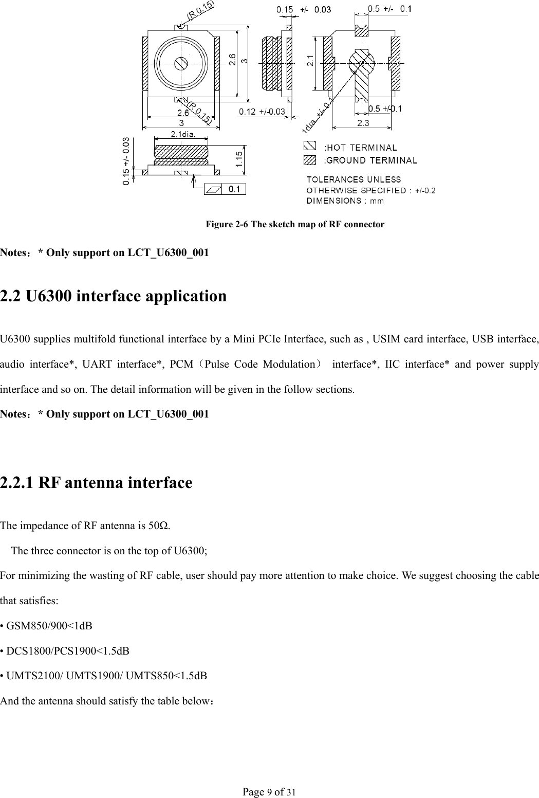
Longcheer Technology U6300 GSM/WCDMA HSPA Module User Manual U6300 UserMan
Shanghai Longcheer Technology Co., Ltd. GSM/WCDMA HSPA Module U6300 UserMan
UserManual.wiki
>
Longcheer Technology
>
U6300 User Manual
User Manual
Navigation menu
Upload a User Manual
Namespaces
Wiki Guide
HTML
PDF
Info
Views
User Manual
Discussion / Help
Navigation

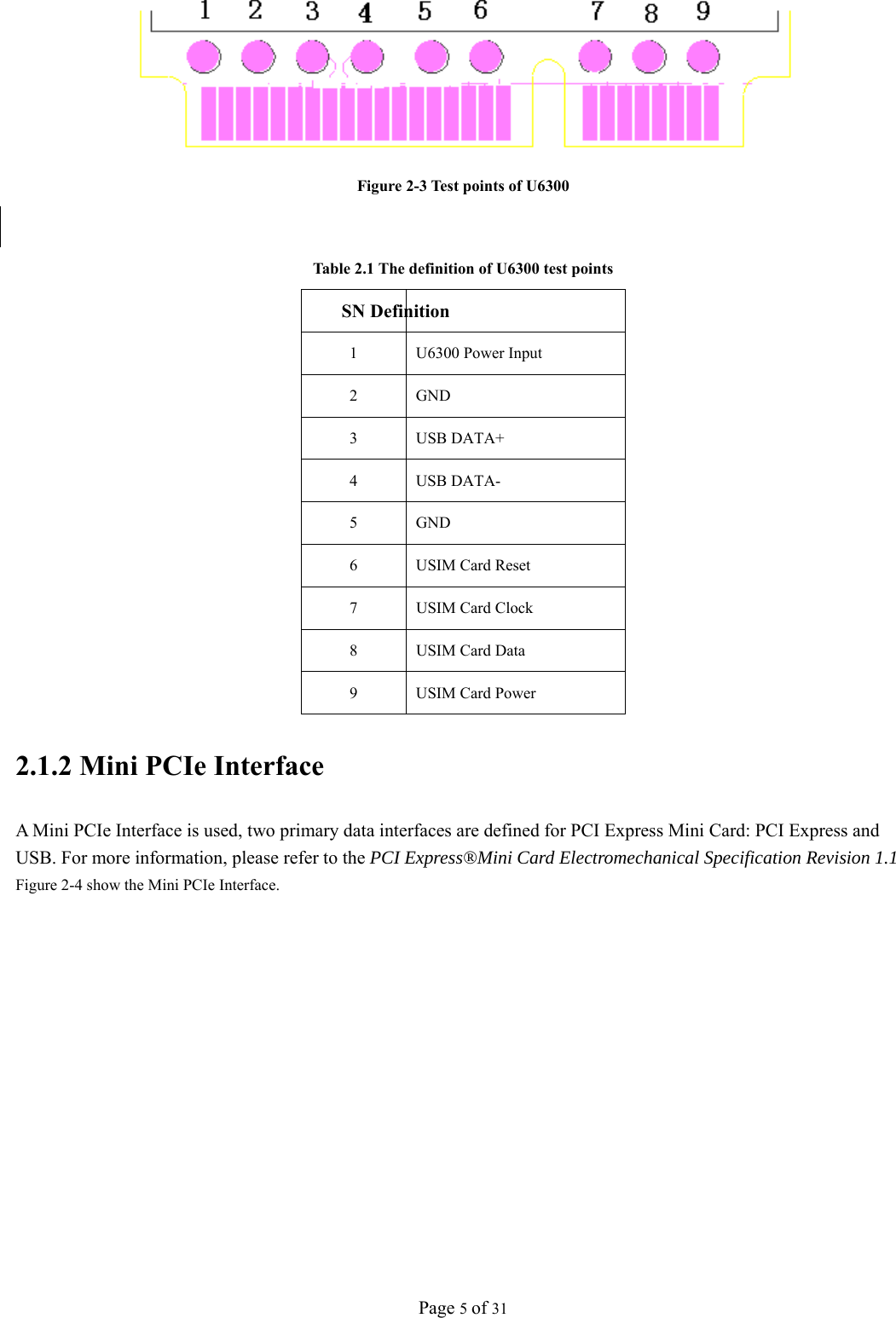
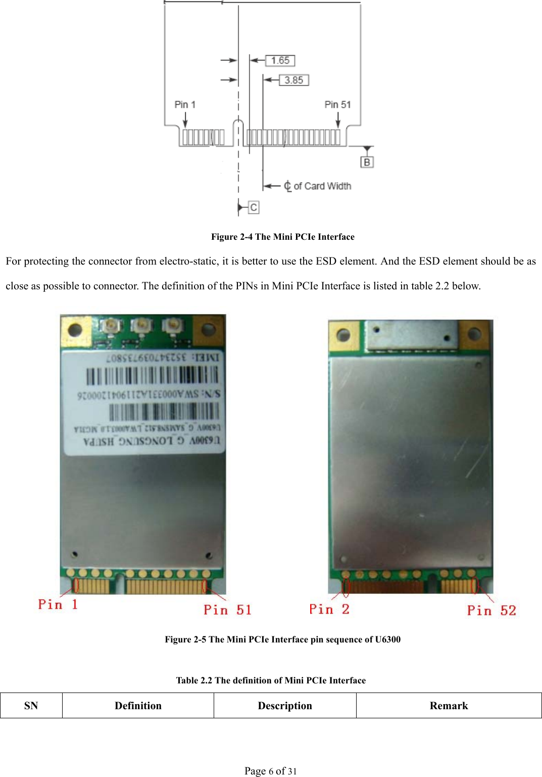
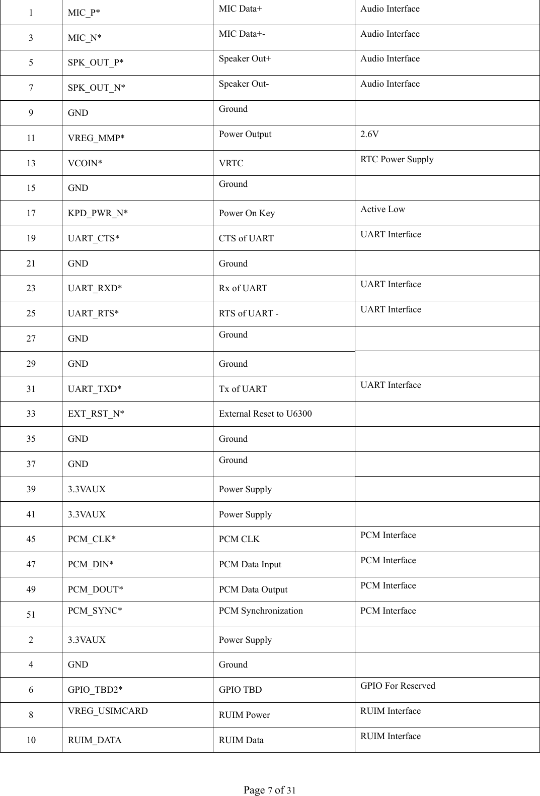
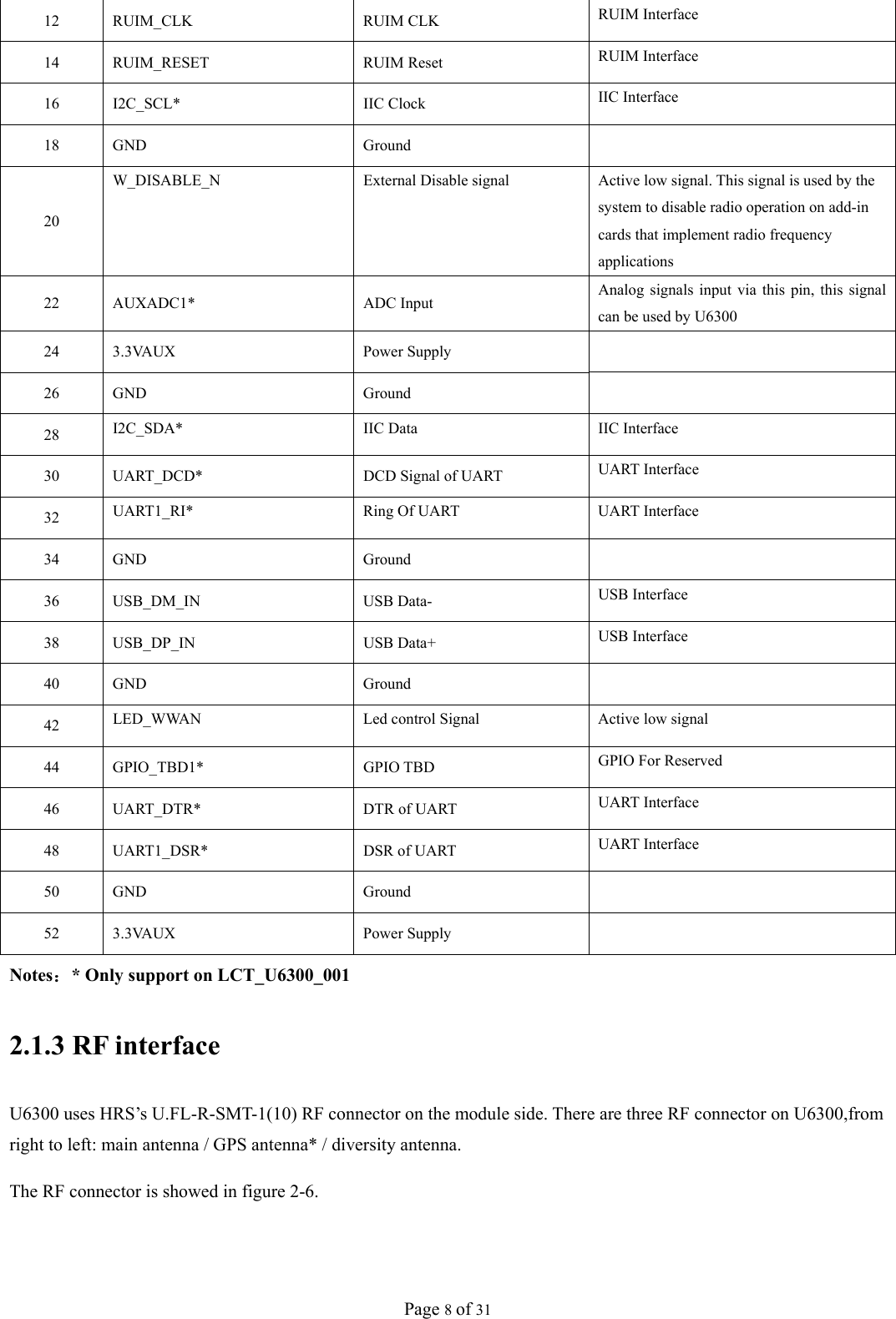
![Page 22 of 31 The related AT commands are listed as follow: ·New Message Indication: AT+CNMI ·Message Send: AT+CMGS ·Message Preview: AT+CMGPR ·Message Delete: AT+CMGD ·Message format Switch: AT+CMGF ·Service Center Address Set: AT+CSCA ·Receiving Message Report enable/disable: AT+CNMI=2,1,0,1,0 3.3 GPS GPS functions are only available in the U6300_001 module. The related AT command as follow: AT+GPSFIX originate GPS request AT+GPSCFG configure GPS parameter 3.4 Phonebook The Phonebook feature is implemented by AT commands. You can set the phonebook storage location, read phone number, write phone number and delete phone number and so on. The related AT commands are listed as follow: AT+CPBS=<storage> set the storage location AT+CPBR=<index> read phone number AT+CPBW=[<index>][,<number>[,<type>[,<text>]]] write phone number on the phone. AT+CPBW=[<index>] delete phone number. AT+CPBF=<findtext> find the phone number according to the findtext. 3.5 AUDIO PCM data path selection The audio functions are only available in the U6300_001 module. The related AT command as follow: The function make user can select audio PCM data path. The user use the related AT commands to select AUDIO PCM data path and so on. The related AT commands as follow: AT+PCMAUDIO=0 select the audio path in the U6300; AT+PCMAUDIO=1 select the external PCM path. AT+PCMAUDIO? check the current audio path in use.](https://usermanual.wiki/Longcheer-Technology/U6300/User-Guide-1499876-Page-22.png)
![Page 28 of 31 3 S AT+CSMP=17,167,0,8 Set the TP-Validity-Period as 167 (24 hours) ,and the SMS Data Coding Mode as UCS2 4 R OK Remark: 1) TP-MTI supports SMS-DELIVER, SMS-SUBMIT and SMS-STATUS-REPORT, while not support SMS- DELIVER-REPORT, SMS-SUBMIT-REPORT and SMS-COMMAND. 2) TP-PID is 0 by default while TPDU is sending or saving. 3) The Min. length of <pdu> is 8 and the Max. length of <pdu> is 164 while TPDU is sending or saving,. 4) The parameter <stat> can only be 2 for the command AT+CMGW. 5) In TEXT Format, the parameter <fo> can be 17 and 49, the parameter <pid> can only be 0, the parameter <dcs> can be 0~31 and the parameter <vp> can be 0~255 for AT+CSMP command 6) In TEXT Format, the parameter <stat> can only be ”STO UNSENT” for the command AT+CMGW 4.3 PHONE BOOK 4.3.1 Set Phone Book Storage Location Phone book storage location can be set by AT command AT+CPBS. The AT command can be used in three ways. Performing AT+CPBS? will return the current storage location of the phone book. Such as +CPBS:<storage>[,<used>,<total>].The parameter <total> indicated how many phone numbers can be stored on the phone. The parameter <used> indicates how many phone numbers have been stored. Performing AT+CPBS=? will return all the storage type which the phone supports. Such as +CPBS:(list of supported <storage>s). We can use AT+CPBS=<storage> to set storage location. There are six types storage location. It’s follow as: “LD” --store the recently call number which have dialed (SIM). “MC” --store the recently call number which haven’t answered. “RC” --store the recently call number which have been answered. “ON” -- store the phone number of itself. “ME” --NVRAM storage “SM” --SIM storage 4.3.2 Read Phonebook entries When you want to read phonebook entries, you can use AT command AT+CPBR. Performing AT+CPBR=? will list of supported index, phone number length and text length. Performing AT+CPBR=<index1>[,<index2>] will return the content of the phonebook entry of index1. If we use](https://usermanual.wiki/Longcheer-Technology/U6300/User-Guide-1499876-Page-28.png)
![Page 29 of 31 index1 and index2 at the same time ,it will return all the entries between index1 and index2. Such as [+CPBR:<index1>,<number>,<type><text>[[...]<CR><LF>+CPBR:<index2>,<number>,<type><text>]] The parameter <type> include 129 and 145.145 indicate which is a international phone number. 129 indicate which is a unknown type number. The parameter <text> is the tag of the number. 4.3.3 Write phonebook entry When you want to write a phonebook entry on the phone, you can use AT commande AT+CPBW. Performing AT+CPBW=? will return list of supported index, max length of phone number, list of supported phone number types and max length of text. We can use the command “AT+CPBW=[<index>][,<number>[,<type>[,<text>]]]” to write number on the phone. If the parameter <number> is NULL, the command will delete the phone number on the phone of index. 4.3.4 Find phonebook entries We can use AT command AT+CPBF when we want to find the entry according to the text. Performing AT+CPBF=? will return the max length of phone number and the max length of text. Such as +CPBF:[<nlength>],[<tlength>]. When we want to find a entry, we can give the text of the phone number ,and according to the text, we use AT+CPBF=<findtext> to find the number we want. 4.4 AUDIO Audio functions are only available in the U6300_001 module. 4.4.1 AUDIO PCM data path selection We can use one of two option to select audio PCM data path. 1) audio path in the U6300. 2) the external PCM interface. The audio PCM data could be routed to external PCM interface and be input from external PCM interface. In this case, the audio path in the U6300 will be switch off. If user wants to use the external PCM audio path, then a CODEC IC must be used, and be connected to the external PCM interface of the U6300. The AT command AT+PCMAUDIO can be used to select which audio path we want to use: AT+PCMAUDIO=0, will select the audio path in the U6300; AT+PCMAUDIO=1, will select the external PCM path. AT+PCMAUDIO?will check the current audio path in use. All the values will not be saved after power off U6300,the default value is 0 while power on the U6300 , namely the default audio path is the audio path that in the U6300.](https://usermanual.wiki/Longcheer-Technology/U6300/User-Guide-1499876-Page-29.png)
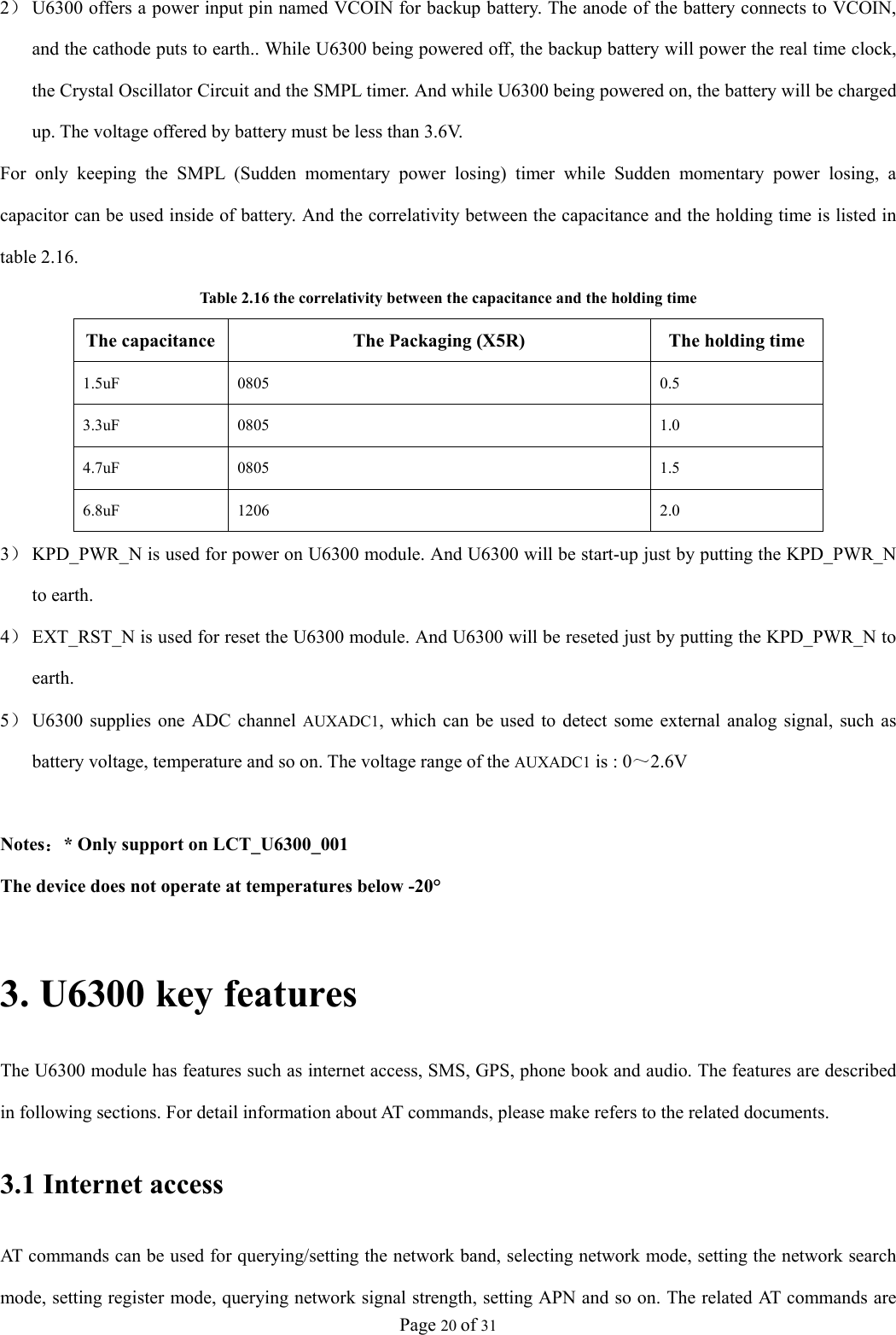
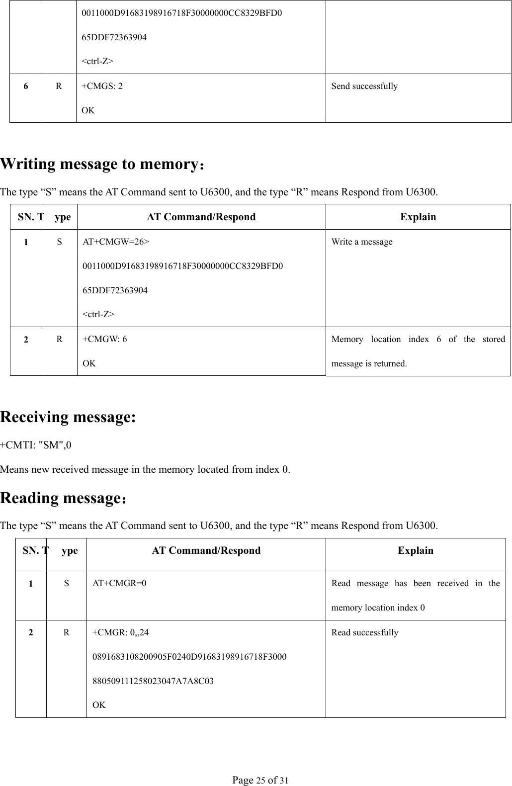
![Page 30 of 31 4.4.2 Originate Call ATD<str>[;] Mobile originate call to dial a number. <str>: string of dialing digits, dialing digits:0~9 <;> only required to set up voice call , return to command state. The Max length of dialing digits is 20; The prefix ”+” is not counted to the length of dialing digits. 4.4.3 Answer a incoming call ATA using the command can answer a incoming call. ATA responds coming call by RING. It will display the calling phone number if CLIP (Calling Line Identity Indication Presentation) function is set. ATA will return NO CARRIER for responding hang up after connection. 4.4.4 Disconnect call AT+CHUP using the command can disconnect a connection. Appendix:Mechanical dimensions of U6300 The following are Mechanical dimensions of U6300 bottom view, side view and top view. (Unit: mm) Top View Side View Bottom View](https://usermanual.wiki/Longcheer-Technology/U6300/User-Guide-1499876-Page-30.png)