LumenRadio CRMXTIMO101 2.4G Wireless Control Module User Manual 1502 ver20
LumenRadio AB 2.4G Wireless Control Module 1502 ver20
Contents
- 1. User manual part 1
- 2. User manual part 2
User manual part 1
Ͳ1Ͳ
TiMo RX RDM 200-1502̢ specifications
Revision A – October 2, 2014
CONFIDENTIALITY NOTE
ThisdocumentmaynotberedistributedwithoutpriorwrittenpermissionfromLumenRadioAB.
GENERAL
CRMX™isthefutureofwirelessDMXdistribution–awirelesssystemthatcommunicatesreliablywithperfect
fidelity.CRMXisthemostpowerfulwirelesslightingcontrolsystemonthemarket,withgroundbreaking
featurestoensureunrivalledreliability.CRMXdistributesDMXandRDM,withfullframeintegrityandprovides
rangeandreliabilitythatsurpassallothersystemsavailabletoday.Thisdocumentdescribesthefunctionand
specificationsoftheTiMoRXRDMreceivermodule.

Ͳ2Ͳ
Table of Contents
Introduction ....................................................................................................... 4
Features ............................................................................................................. 4
Pin assignments and functions ...........................................................................5
Pin assignments ................................................................................................................................... 5
Pin functions ........................................................................................................................................ 6
Typical application circuit ...................................................................................7
Reference design files ........................................................................................ 8
PCB mounting .................................................................................................... 8
Internal or External Antenna? ................................................................................................................ 8
Internal Antenna .............................................................................................................................. 8
Layout considerations for the main (Customer) board. .............................................................................. 8
Layout Example ................................................................................................................................... 9
TiMo reflow soldering specification ........................................................................................................ 11
LED outputs ......................................................................................................12
Status ............................................................................................................................................... 12
Linked .............................................................................................................................................. 12
RF Link ............................................................................................................................................. 12
DMX ................................................................................................................................................. 12
RDM LED ........................................................................................................................................... 12
Radio level ........................................................................................................................................ 13
Link switch input ..............................................................................................13
Antenna selection ............................................................................................ 13
SPI interface .................................................................................................... 14
Interface description ........................................................................................................................... 14
Bit and byte order .......................................................................................................................... 14
Clock polarity ................................................................................................................................ 14
Maximum clock speed ..................................................................................................................... 14
Setup time .................................................................................................................................... 14
SPI operation ..................................................................................................................................... 14
SPI transactions ............................................................................................................................. 14
SPI commands .............................................................................................................................. 15
Interrupts ......................................................................................................................................... 17
RX_DMX_IRQ ................................................................................................................................ 17
LOST_DMX_IRQ ............................................................................................................................. 17
DMX_CHANGED_IRQ ...................................................................................................................... 17
RF_LINK_IRQ ................................................................................................................................ 17
ASC_IRQ ....................................................................................................................................... 17
DMX Window register.......................................................................................................................... 17
Antenna selection ............................................................................................................................... 17
Version register ................................................................................................................................. 18
Hardware revision .......................................................................................................................... 18
Driver version .................................................................................................................................... 18
Binding UID ....................................................................................................................................... 18
DMX Interface .................................................................................................. 19
SPI ................................................................................................................................................... 19
DMX window.................................................................................................................................. 19
Reading DMX data over SPI ............................................................................................................. 19
UART DMX/RDM interface .................................................................................................................... 19
DMX and RDM termination and line bias ................................................................................................ 19
DMX frame rate and size ..................................................................................................................... 20
DMX start codes ................................................................................................................................. 20
RDM start code frames........................................................................................................................ 20
Alternate start code frames ................................................................................................................. 20
Reading ASC data over SPI ............................................................................................................. 21
Output Power ................................................................................................... 22

Ͳ3Ͳ
Radio driver update ..........................................................................................22
Specifications ................................................................................................... 23
Product marking............................................................................................... 24
Product documentation and menu systems ...................................................... 24
Logo Syndication .............................................................................................. 24
Design Verification ........................................................................................... 24
Production Testing ........................................................................................... 25
Compliance information ................................................................................... 25
FCC information ................................................................................................................................. 25
FCC Information to User ................................................................................................................. 25
FCC Guidelines for Human Exposure ................................................................................................. 25
FCC Declaration of Conformity ......................................................................................................... 25
FCC Radio Frequency Interference Warnings & Instructions ................................................................. 25
Industry Canada statement ................................................................................................................. 26
CE .................................................................................................................................................... 26
Compliance Marking ........................................................................................................................... 26
FCC & Industry Canada ................................................................................................................... 26
Other Compliances ......................................................................................................................... 27
Order codes ......................................................................................................28
LumenRadio Contacts .......................................................................................28
Mechanical specifications ................................................................................. 29
TiMo RX RDM ..................................................................................................................................... 29
Revision history ............................................................................................... 30

Ͳ4Ͳ
Introduction
CRMX™1 is an acronym for Cognitive Radio MultipleXer and is the first smart wireless
system to automatically and continuously adapt to its surroundings in real time. CRMX
was specifically developed to meet the demand for reliable, easy to use, and cost
effective wireless lighting controls.
LumenRadio launched its unique CRMX wireless technology for sale on an OEM basis in
April of 2009. CRMX has since then been the only smart radio that automatically adapts
to its surroundings in a smart way.
CRMX has been developed by veterans in the wireless lighting control business with
years of experience of the high demands of the entertainment and architainment
businesses.
CRMX is now also available for OEM implementations as an even more cost effective and
space effective surface mounted solution providing wireless DMX receiving capabilities to
the most cost and/or space sensitive applications.
The TiMo RX RDM receiver is a highly integrated wireless DMX receiver module and is
compatible with all LumenRadio CRMX transmitter as well as W-DMX™2 G2, G3, G4 and
G4Stransmitters (G4 and G4S in 2.4 GHz mode only).
Features
xSupports ANSI E1.11 - DMX512-A and ANSI E1.20 - RDM
xCognitive coexistence – dynamically avoids occupied frequencies
xDMX fidelity and frame integrity
xDMX frame rate and frame size auto sensing
xFixed 5 ms end-to-end latency
xAutomatic legacy (W-DMX G3, G4 and G4S) compatibility mode
xSmall footprint 18.5 mm x 33.5 mm
xIntegral chip antenna and U.FL/IPEX external antenna connector
xAll configuration data is stored in non-volatile memory, 20 years data retention
xTiMo RX RDMcontains upgradeable drivers for future proofing
xOver-the-air driver upgrades
1CRMXisatrademarkofLumenRadioAB
Othertrademarksandtradenamesarethepropertyoftheirrespectiveholder
2WͲDMXisatrademarkofWirelessSolutionSwedenAB
Pin
a
This se
Pin a
Figure
a
ssig
n
ction desc
r
ssignm
e
1: TiMo RX
n
ment
s
r
ibes the pi
e
nts
RDM pino
u
s
and
f
n assignm
e
u
t.
Ͳ5Ͳ
f
uncti
o
e
nts and pi
n
o
ns
n
function
s
s
.

Ͳ6Ͳ
Pin functions
Pin Name Function Description
1 VSS Power Ground (0V)
2 /IRQ Digital output Interrupt signal, active low
3 /CS Digital input Chip select, active low
4 SCK Digital input SPI clock
5 MOSI Digital input SPI Master Out, Slave In
6 MISO Digital output SPI Master In, Slave Out
7 VSS Power Ground (0V)
8 DMX_TXD Digital output DMX TXD
9 VSS Power Ground (0V)
10 RS485_DE Digital output RS485 driver control signal
11 /RS485_RE Digital output RS485 driver control signal
12 DMX_RXD Digital input DMX RXD (3.3 V max)
13 RDI_LVL0 Digital output Radio level LED
14 RDI_LVL1 Digital output Radio level LED
15 RDI_LVL2 Digital output Radio level LED
16 RDI_LVL3 Digital output Radio level LED
17 RDI_LVL4 Digital output Radio level LED
18 RDM Digital output RDM LED
19 DMX Digital output DMX LED
20 N.C. No connection
Do not connect
21 N.C. No connection
Do not connect
22 VSS Power Ground (0V)
23 VSS Power Ground (0V)
24 VSS Power Ground (0V)
25 VSS Power Ground (0V)
26 VSS Power Ground (0V)
27 VSS Power Ground (0V)
28 VSS Power Ground (0V)
29 VSS Power Ground (0V)
30 VSS Power Ground (0V)
31 ANT_SEL Digital input RF Antenna select
32 LINK_SW Digital input Link control switch input
33 STATUS_LED
Digital output Status LED
34 LINKED Digital output Linked to transmitter LED
35 RF_LINK Digital output RF link LED
36 VDD Power Power supply (3.3V)
37 VSS Power Ground (0V)
ANT RF ANT RF Antenna connector
Ͳ7Ͳ
Typical application circuit
Figure 2: Typical application circuit for TiMo RX RDM
U2
SN65176B
R1
RE 2
DE 3
D4
Vcc
8B
7A
6GND
5
5V
C1
100nF
R1
6k8
R2
3k9
DMX-
5V-3V3
volt div
U1
CRMX_TiMo
VSS1
1
IRQ
2
CS
3
SCK
4
MOSI
5
MISO
6
VSS2
7
DMX_TXD
8
VSS3
9
RS485_DE
10
RS485_RE
11
DMX_RXD
12
RDI_LVL0
13
RDI_LVL1
14
RDI_LVL2
15
RDI_LVL3
16
RDI_LVL4
17
RDM_LED
18
DMX_LED
19
NC1
20
NC2
21
VSS4
22
VSS5
23
VSS6 24
VSS7 25
VSS8 26
VSS9 27
VSS10 28
VSS11 29
VSS12 30
ANT_SEL 31
LINK_SW 32
STATUS_LED 33
LINKED_LED 34
RF_LINK_LED 35
VDD 36
VSS13 37
3V3
SPI bus to fixture CPU
DMX+
R4
130
R3
562
5V
R5
562
S
PI
b
u
s
to
fi
xt
ur
e

Ͳ8Ͳ
Reference design files
A complete reference design including PCB layout and PCB design guidelines is available
from LumenRadio to make integration easier. Please send your inquiry to LumenRadio
for details.
PCB mounting
Internal or External Antenna?
For short distances the modules´ internal antenna will perform well. But if the design is
to be placed inside a metal enclosure, or if there is a need to cover large distances, an
external antenna is necessary. An external antenna MUST at least be designed for
operation between 2.4 – 2.48GHz
Always use external antennas with a 50ς characteristic impedance.
Internal Antenna
If the internal antenna is considered, the product case needs to be of a RF transparent
plastic material. The circuit board that will hold TiMo needs to be designed so that the
internal chip antenna radiates efficiently. Avoid any ground planes near the antenna chip.
When placing TiMo on a circuit board:
xPlace the module as close to the host circuit board edge as possible with the
antenna pointing outward.
xNote the absence of ground plane near the chip antenna on the modules´ circuit
board.
xRemove any copper from the main board as specified in section “Layout
ExampleLayout Examples”
xAvoid using metal structures such as mounting hardware close to the antenna
chip.
Layout considerations for the main (Customer) board.
TiMo has been specifically designed in order to achieve good RF performance. In order to
maintain this, there are some guidelines that we would like to stress:
The use of ground planes also on the main board cannot be overemphasized. Good
decoupling of any high speed digital circuitry is a must. Many embedded type
microprocessors today has clock frequencies with clocks or over tones that reaches well
into the GHz range. It is perfectly possible for an embedded design to pass any EMC
certification and still cause disturbances that will block the RF reception of the TiMo
module. The sensitivity of the TiMo receiver is -96dBm therefore it is recommended to
keep disturbances below -100dBm in the frequency range of operation
ᑖṬᔿⲴ
Ͳ9Ͳ
A near field probe connected to a spectrum analyzer will show if there are any
disturbances present on the 2.45 GHz band generated by the microprocessor or any
other device that is placed on the main board. Pay special attention to readymade LAN-
products "Server in a RJ connector". They pass EMC certifications, but some of them
radiates badly on 2.45 GHz. If disturbances can be seen on a spectrum analyzer - then
the TiMo module will have impaired reception.
TiMo has a supply voltage decoupling on the circuit board. The supply voltage still needs
to be adequately filtered. If any disturbance or intermittent communication failures occur,
as one of the trouble shooting steps - check the supply voltage for drop-outs, switch
supply ripple etc.
Layout Example
1. The TOP layer inside the footprint must be free from copper. There is a ground
plane on TiMo, but there are also supply lines. It is an unnecessary risk to rely on
solder mask lacquer for isolation.
2. The area around the antenna must be kept clear from copper on all layers. This is
shown in the picture below. This shows inner layer 1 (next to TOP)

Ͳ10Ͳ
Minimum dimensions for ground plane clearance for optimum antenna performance are
shown below:
6.
8
m
7.5mm
Placeoncardedgefor
optimumantenna
performance
16
m
m
Ͳ11Ͳ
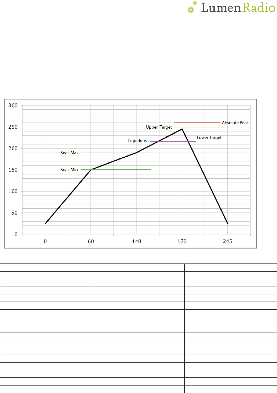
TiMo reflow soldering specification
TiMo is a surface mount device (SMD) designed to be easily manufactured including
reflow soldering to a PCB.It isultimately theresponsibility of the customer to choose the
appropriate solder paste and to ensure oventemperatures during reflow meet the
requirements of the solder paste. TiMo surface mount module conforms to JSTD-020D1
standards for reflow temperatures.
Temperatures should not exceed the minimums or maximums presented in table below:
SpecificationValue
Unit
TemperatureInc./Dec.Rate(max)1~3°C/sec
TemperatureDecreaserate(goal)2Ǧ4°C/sec
SoakTempIncreaserate(goal).5
Ǧ
1°C/sec
Flux
SoakPeriod(min)70sec
FluxSoakPeriod(max)120sec
FluxSoakTemp(min)150°C
FluxSoakTemp(max)190°C
TimeAboveLiquidous(max)70sec
TimeAboveLiquidous(min)50sec
TimeInTargetReflowRange
(goal)
30sec
TimeAtAbsolutePeak(max)5sec
LiquidousTemperature(SAC305)218°C
LowerTargetReflowTemperature
225°C
UpperTargetReflowTemperature
250°C
AbsolutePeakTemperature260°C
Ͳ12Ͳ
LED outputs
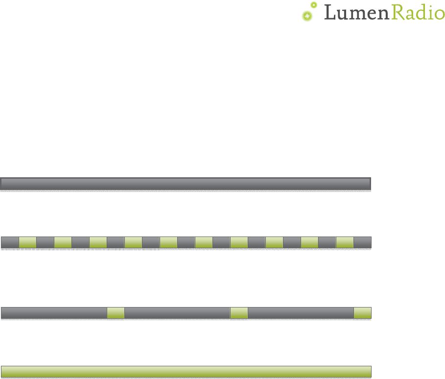
Status
The status LED (STATUS_LED) indicates the status of the TiMo RX RDM. The LED
indicator pin is an output pin capable of sourcing 5mA at the VDD voltage. An appropriate
current limiting resistor must be connected in series with the LED.
Constant off (0V): Not linked to any transmitter
Flashing: off (0V) 100 ms / on (VDD) 100 ms: linked to a transmitter, but no active radio
link
Flashing: off (0V) 900 ms / on (VDD) 100 ms: Active radio link, no DMX present
Constant on (VDD): Active radio link, DMX data present
Linked
The Linked LED (LINKED) indicates whether the TiMo RX RDM is linked to a transmitter
or if it’s available to be linked. High level (VDD) on this pin indicates a linked state; low
level (0V) indicates that the TiMo RX RDM is not linked.
RF Link
A high level (VDD) on the RF Link LED output (RF_LINK) indicates that the TiMo RX RDM
is within range from the transmitter it is linked to and that an active radio link from the
transmitter is present.
DMX
The DMX LED (DMX_LED) indicates if a valid DMX stream is received from the
transmitter. A high level (VDD) indicates that DMX is present, a low level (0V) indicates
that no valid DMX is present.
RDM LED
A high level (VDD) on the RDM LED output (RDM_LED) indicates that the TiMo RX RDM is
performing RDM activity.

Ͳ13Ͳ
Radio level
TiMo RX RDM has 5 output signals for controlling radio level LEDs in the form of a bar
graph (RDI_LVL0 - RDI_LVL4). Operation of these, and suggestion of LED colors, can be
found in the table below.
Signal name Suggested LED color On when signal quality
RDI_LVL0 Red below ~10%
RDI_LVL1 Amber / Yellow above ~20%
RDI_LVL2 Green above ~40%
RDI_LVL3 Green above ~60%
RDI_LVL4 Green above ~80%
Link switch input
The link switch input can be used to interface with a momentary closing push button to
facilitate a simple user interface when not using the SPI interface to integrate into a host
device’s menu system.
Please refer to the example schematic for details on how to connect the push button.
This signal shall be pulled to VDD using an external 4.7kȍ-10kȍ resistor, when used, to
ensure proper function.
The switch input has two functions: unlink the receiver from a transmitter or to force
driver update mode. Please see the table below for details about the functions of the
switch input.
Function Conditions
Unlink from
transmitter Hold signal low (button pressed) for >3 seconds.
Force driver
update mode Hold signal low (button pressed) during power on.
Antenna selection
The antenna selection input can be used to select the required RF antenna for use on
TiMo RX RDM. This pin is internally pulled high. This pin can be overridden by writing the
ANTENNA register.
State Conditions
High Level
(Logical 1) External U.FL/IPEX connector
Low Level
(Logical 0) Internal Chip Antenna
Ͳ14Ͳ
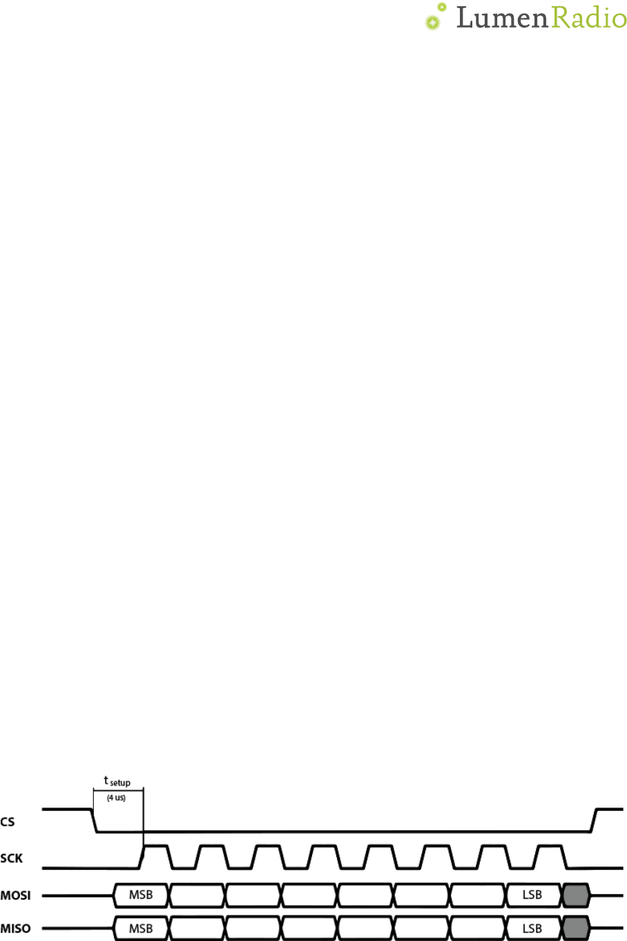
SPI interface
The SPI interface gives access to all features of the TiMo RX RDM. The interface consist
of five digital signals (VDD max):
xIRQ – Interrupt signal. Active low, configurable through the interrupt mask
register.
xCS – SPI Chip select, active low.
xSCK – SPI clock input
xMOSI – SPI data input
xMISO – SPI data output
Interface description
Bit and byte order
The data on the SPI bus is clocked with most significant bit first. All multi-byte register
data are sent in big-endian byte order.
Clock polarity
Data is valid in the low-to-high transition of SCK. This is also known as the clock being
active high with valid data on the leading clock edge.
Maximum clock speed
The maximum clock speed supported by TiMo RX RDM is 2MHz. Clock speeds above this
limit may result in unexpected behavior.
Setup time
The SPI slave unit has a setup time of 4 Njs after the high-to-low transition of the CS
signal.
SPI operation
SPI transactions
All SPI transactions start with a high-to-low transition on the CS pin. The CS pin must be
held low during the entire SPI transaction.
The IRQ_FLAGS register is always shifted out as the first byte of each transaction.
Figure 3: Example SPI transaction
Ͳ15Ͳ
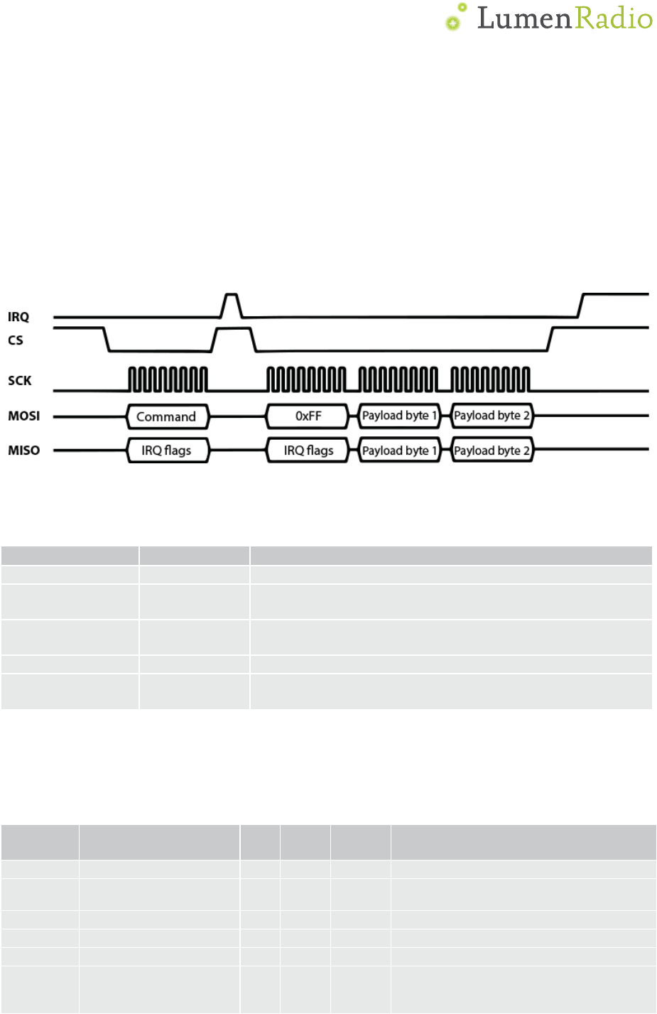
SPI commands
All SPI command sequences, except for the NOP command, consist of two SPI
transactions. The first transaction shall be one byte long, this is the command byte. The
second transaction is the payload. The second transaction must not be started until the
TiMo RX RDM has confirmed the command by a high-to-low transition on the IRQ pin.
The first byte being sent to TiMo RX RDM in the second transaction will be ignored,
however it is suggested this byte is being sent as 0xFF. See below for an example full
SPI command sequence.
NOTE: Bit 7 in the IRQ flags register MUST be observed. A ‘1’ in this bit means that the
SPI slave module is unable to process the current transaction, and the full command
sequence MUST be restarted – this means sending the command transaction again.
Figure 4: Example SPI command sequence with a pending IRQ when sequence started
The available SPI commands are listed in the table below.
Command Binary value Comment
WRITE_REG 01AA AAAA Write to a register. AAAAAA = 6 bit register address
READ_REG 00AA AAAA Read from a register. AAAAAA = 6 bit register
address
READ_DMX 1000 0001 Read the latest received DMX values from the window
set up by the DMX_WINDOW register.
READ_ASC 1000 0010 Read the latest received ASC frame.
NOP 1111 1111 No operation. Can be used as a shortcut to read the
IRQ_FLAGS register.
Registermap
All undefined bits in the table below shall be considered reserved for future use - don’t
care when read, write as 0.
Do not read or write undefined registers – doing so could result in undefined behavior.
Address
(hex) Mnemonic Bit
# Type
Reset
value Description
00 CONFIG Configuration register
UART_EN 0 R/W 1 Enable UART output of DMX frames
(required for RDM)
Reserved 1-6
- - Reserved for future use
RX_ENABLE 7 R/W 1 Enable wireless DMX reception
01 STATUS Status register
LINKED 0 R/W - 0 = Not linked, 1 = Linked to TX (or
pairing)
Write 1 to unlink