LuxLabs MeshNetics ZIGBIT-B0 2.4GHz 802.15.4/ZigBee OEM-module User Manual Product Datasheet
LuxLabs Ltd. dba MeshNetics 2.4GHz 802.15.4/ZigBee OEM-module Product Datasheet
Manual
DOC. M-251~01 V.1.9 WWW.MESHNETICS.COM APRIL 2007
© 2007 MeshNetics
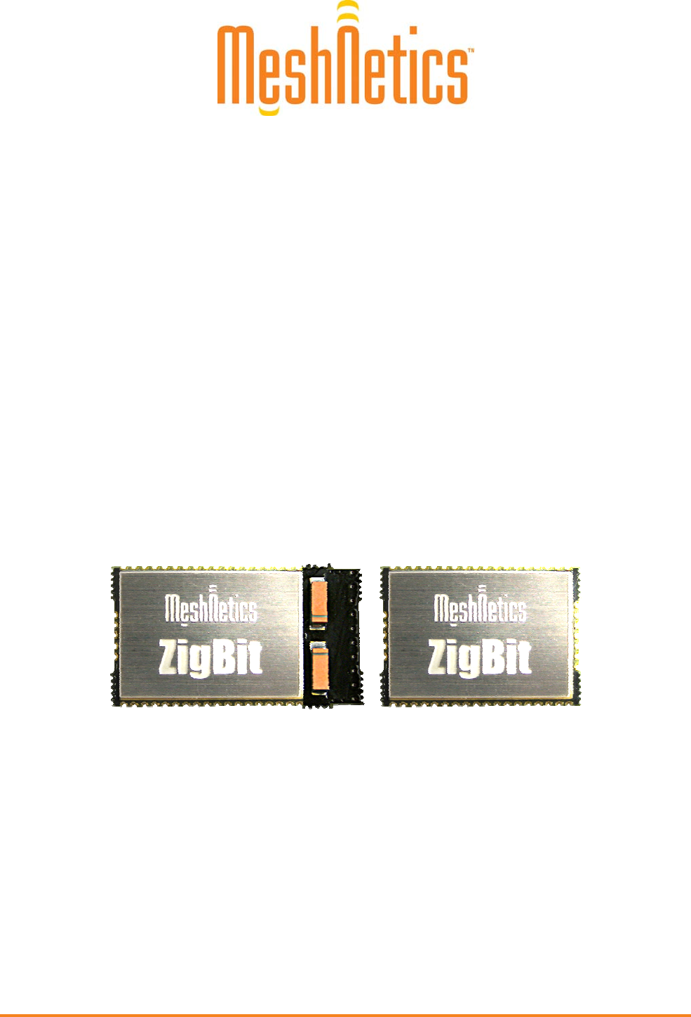
ZigBit™ OEM Modules
ZDM-A1281-*
Ultra-Compact 2.4GHz 802.15.4/ZigBee Modules
for Wireless Networking Applications
Product Datasheet

ZigBit™ OEM Modules Product Datasheet
© 2007 MeshNetics Page 2 of 22
Table of Contents
Summary .............................................................................................................................................................3
Applications ........................................................................................................................................................3
Key features ........................................................................................................................................................3
Benefits................................................................................................................................................................3
ZigBit™ Module Overview .................................................................................................................................4
Specifications .....................................................................................................................................................5
Absolute Maximum Ratings*** ..........................................................................................................................6
Physical/Environmental Characteristics and Outline.....................................................................................7
Pin Configuration................................................................................................................................................8
Mounting Information.......................................................................................................................................12
Sample Antenna Reference Designs..............................................................................................................13
Agency Certifications.......................................................................................................................................18
Technical Support ............................................................................................................................................20
Development Support ......................................................................................................................................20
Ordering Information........................................................................................................................................20
Related Documents ..........................................................................................................................................21
Disclaimer..........................................................................................................................................................21
Trademarks .......................................................................................................................................................21
Contact Information..........................................................................................................................................21

ZigBit™ OEM Modules Product Datasheet
© 2007 MeshNetics Page 3 of 22
Summary
ZigBit™ stands for ultra-compact, low-power, high-sensitivity 2.4GHz 802.15.4/ZigBee 2006 OEM modules from
MeshNetics, based on the innovative Atmel’s mixed-signal hardware platform. They are designed for wireless
sensing, control and data acquisition applications. The ZigBit modules eliminate the need for costly and time-
consuming RF development, and shorten time to market for a wide range of wireless applications.
Two different versions of ZigBit modules are available: ZDM-A1281-B0 module with balanced RF port for
applications where the benefits of PCB or external antenna can be utilized and ZDM-A1281-A2 module with chip
antenna satisfying the needs of size sensitive applications.
Applications
ZigBit features standards-based networking stack, based on IEEE802.15.4 PHY and MAC layers, and ZigBee
NWK/APS/ZDO layers. It enables multipoint, multihop communications over an area of thousands of square meters
at moderate data rates without expensive infrastructure support. The architecture of the Wireless Sensor Networks
(WSN) allows for use of low powered devices. The applications include, but are not limited to:
• Building automation & monitoring
• Lighting controls
• Wireless smoke and CO detectors
• Structural integrity monitoring
• HVAC monitoring & control
• Inventory management
• Environmental monitoring
• Security
• Water metering
• Industrial monitoring
• Machinery condition and performance monitoring
• Monitoring of plant system parameters such as
temperature, pressure, flow, tank level, humidity,
vibration, etc.
• Automated meter reading (AMR)
Key features
• Ultra compact size (24 x 13.5 mm for
ZDM-A1281-A2 module and 18,8 x 13.5 mm for
ZDM-A1281-B0 module)
• Innovative (patent-pending) balanced chip antenna
design with antenna gain of approximately 0 dBi
(for ZDM-A1281-A2 version)
• High RX sensitivity (-101 dBm)
• Outperforming link budget (104 dB)
• Up to 3 dBm output power
• Very low power consumption
(<6 µA in deep sleep mode)
• Ample memory resources (128 kBytes of flash
memory, 8 kBytes RAM, 4 kBytes EEPROM)
• Wide range of interfaces (both analog and digital):
• 10 spare GPIO, 2 spare IRQ lines
• 4 ADC lines
• UART with CTS/RTS control
• I
2C, USART/SPI
• Up to 30 lines can be configured as GPIO
• Capability to write own MAC address into the
EEPROM
• Optional antenna reference designs
• IEEE 802.15.4 compliant
• 2.4 GHz ISM band
• eZeeNet embedded software, including UART
bootloader and AT command set
Benefits
• Less physical space constraints
• Best-in-class RF link range
• Longer battery life
• Easy prototyping with 2-layer PCB
• More memory for user software application
• Mesh networking capability
• Easy-to-use low cost Evaluation Kit
• Single source of support for HW and SW
• Worldwide license-free operation
ZigBit™ OEM Modules Product Datasheet
© 2007 MeshNetics Page 4 of 22
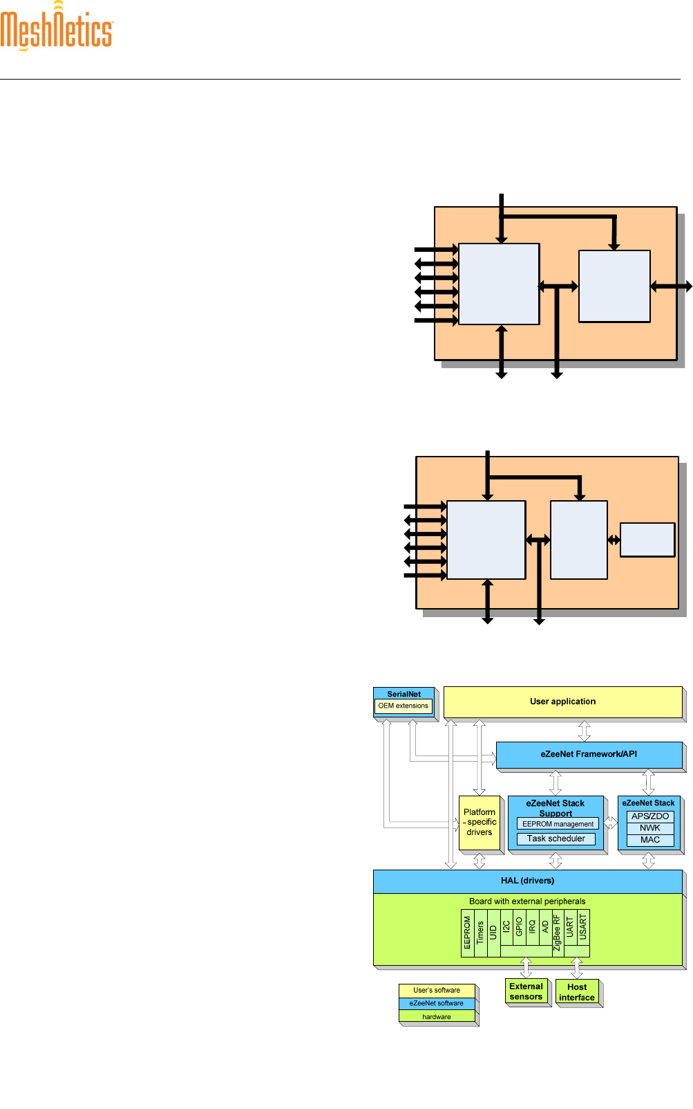
AT86RF230
RF
Transceiver
ATmega1281
Micro
controller RF I/O
SPI BusGPIO
VCC (1.8 – 3.6V)
UART
I2C
JTAG
Analog
IRQ
USART/SPI
ATmega1281
Micro
controller
SPI BusGPIO
VCC (1.8 – 3.6V)
UART
I2C
JTAG
Analog
IRQ
AT86RF230
RF
Transceiver
Chip
Antenna
USART/SPI
ZigBit™ Module Overview
ZigBit is a low-power, high-sensitivity IEEE802.15.4/
ZigBee-2006 compliant OEM module. This multi-
functional device occupies less than a square inch of
space, which is comparable to a typical size of a single
chip. Based on a solid combination of Atmel’s latest AVR
Z-Link hardware platform [1], the ZigBit offers superior
radio performance with exceptional ease of integration.
ZigBit modules comply with the FCC (Part 15), IC and
ETSI (CE) rules applicable to the devices radiating in
uncontrolled environment. For details, see section
Agency Certifications below.
ZigBit fully satisfies the requirements of the “Directive
2002/95/EC of the European Parliament and the Council
of 27January 2003 on the restriction of the use of certain
hazardous substances in electrical and electronic
equipment” (RoHS). MeshNetics provides fully compliant
product in all regions where the directive is enforced July
1, 2006.
The ZigBit contains Atmel’s ATmega1281V
Microcontroller [1] and AT86RF230 RF Transceiver [2].
The module features 128kb flash memory and 8 kb RAM.
The ZigBit already contains a complete RF/MCU-related
design with all the necessary passive components
included. The module can be easily mounted on a simple
2-layer PCB. Compared to a single-chip, a module-based
solution offers considerable savings in development time
& NRE cost per unit during the design & prototyping
phase.
Innovative (patent-pending) chip antenna design in ZDM-
A1281-A2 module eliminates the balun and achieves
good performance over ZigBee frequency band.
MeshNetics provides tools for building ready-to-use
applications around the ZigBit module. The Evaluation
Kit and the Development Kit help prototyping and testing
an 802.15.4 or ZigBee networking solution. It includes
the sensor boards with multiple interfaces, an out-of-the-
box data acquisition software suite, as well as
accessories and documentation. The sample sensor data
acquisition application allows network monitoring and
data collection, all visualized via graphic interface.
The ZigBit modules come bundled with the eZeeNet
networking firmware. The eZeeNet enables the module-
based OEM products to form self-healing, self-organizing
mesh networks. The eZeeNet stack conforms to
IEEE802.15.4/ ZigBee specifications [3], [4], [5].
Depending on your design requirements, you can use
the ZigBit to operate a sensor node, where it would
function as a single MCU. Or you can pair it to a host
processor, where the module would serve essentially as
a modem.
In the former case, a user application should be bundled
with the eZeeNet software. The eZeeNet’s programming
interface gives users flexibility to manage network and
minimize power consumption.
ZDM-A1281-B0 Block Diagram
ZDM-A1281-A2 Block Diagram
eZeeNet™ Block Diagram
ZigBit™ OEM Modules Product Datasheet
© 2007 MeshNetics Page 5 of 22
In the latter case, the host processor can control data transmission and manage module peripherals via powerful set
of AT commands. This way, a minimum engineering effort for development of customer’s devices is required.
Additionally, the sensors can be connected directly to the module, thus expanding the existing set of sensor
interfaces. The over-the-air control via AT-commands makes debugging and network testing easier. It also enables
wireless module configuration during OEM mass-production process and provides flexible commissioning protocol
for installation and maintenance of ZigBit-based devices.
The eZeeNet is compact private profile software from MeshNetics that is specifically tailored for data acquisition
applications. It allows optimizing the network traffic, reducing power consumption, scheduling, and smart power
management. The eZeeNet software comes with a set of drivers for standard peripherals (I2C, GPIO, ADC, etc.) that
ensure the ZigBit module easy integration.
Specifications
Test Conditions (unless otherwise stated): Vcc= 3 V, f=2.45 GHz, Tamb= 25 °C
Module Operating Conditions
Parameters Ran
g
eUnit Condition
Su
pp
l
y
Volta
g
e
(
Vcc
)
1.8 to 3.6 V
Current Consum
p
tion: RX mode 19 m
A
see Note
Current Consum
p
tion: TX mode 18 m
A
see Note
Current Consumption: Radio is turned off,
MCU is active for 50% of the time. 14 mA see Note
Current Consumption: Power Save mode 6 μA see Note
Note: Parameters specified above are measured under the following conditions:
• eZeeNet software is running at 4 MHz clock rate, DTR line management is turned off
• all interfaces are set to the default state (see Pin Assignment Table)
• output TX power is 0 dBm
• JTAG is not connected
• V
cc = 3.0 V
• actual current consumption depends on multiple factors, including but not limited to the board
design and materials, extra MCU load by user application, peripherals usage, EEPROM
reading/writing, eZeeNet settings, network activity and so on.
RF Characteristics
Parameters Ran
g
eUnit Condition
Fre
q
uenc
y
Band 2.400 to 2.4835 GHz
Number of Channels 16
Channel S
p
acin
g
5MHz
Transmitter Output Power -17 to +3 dBm Adjusted in 16
steps
Receiver Sensitivit
y
- 101 dBm PER = 1%
On-Air Data Rate 250 kb
p
s
TX Output / Rx Input Nominal Impedance 100 Ohms For balanced
output

ZigBit™ OEM Modules Product Datasheet
© 2007 MeshNetics Page 6 of 22
ATmega1281V Microcontroller Characteristics
Parameters Ran
g
eUnit Condition
On-Chi
p
Flash Memor
y
Size 128 kB
y
tes
On-Chi
p
RAM Size 8 kB
y
tes
On-Chi
p
EEPROM Size 4 kB
y
tes
O
p
eration Fre
q
uenc
y
4MHz
Module Interfaces Characteristics
Parameters Ran
g
eUnit Condition
UART Maximum Baud Rate 38.4 kb
p
s
ADC Resolution / Conversion Time 10 / 200 Bits / μs In the single
conversion mode
ADC In
p
ut Resistance 100 MOhm
ADC Reference Volta
g
e
(
Vref
)
1.0 to Vcc -0.3 V
ADC In
p
ut Volta
g
e 0
÷
Vref V
I2C Maximum Clock 222 kHz
GPIO Out
p
ut Volta
g
e
(
Hi
g
h/Low
)
2.3 / 0.5 V
(
-10 / 5 mA
)
Real Time Oscillator Frequency 32.768 kHz
Absolute Maximum Ratings***
Parameter Min Value Max Value
Voltage of any Pin except RESET with respect to
Ground -0.5 V Vcc + 0.5 V
DC Current
p
er I/O Pin 40 m
A
DC Current D
_
VCC and DGND Pins 200 m
A
In
p
ut RF Level +10 dBm
***Absolute Maximum Ratings are the values beyond which damage to the device may occur. Under no
circumstances must the absolute maximum ratings given in the following table be violated. Stresses beyond those
listed under “Absolute Maximum Ratings” may cause permanent damage to the device.
This is a stress rating only and functional operation of the device at these or other conditions, beyond those
indicated in the operational sections of this specification, is not implied. Exposure to absolute maximum rating
conditions for extended periods may affect device reliability.
****Caution! ESD-sensitive device. Precaution should be used when handling the device in order to prevent
permanent damage.
ZigBit™ OEM Modules Product Datasheet
© 2007 MeshNetics Page 7 of 22
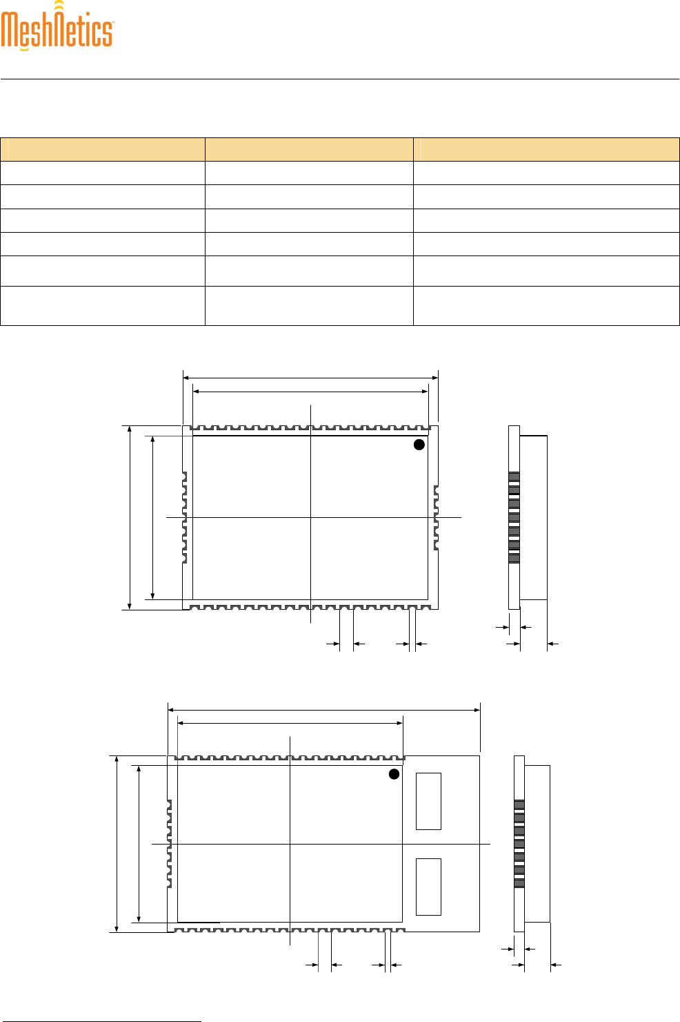
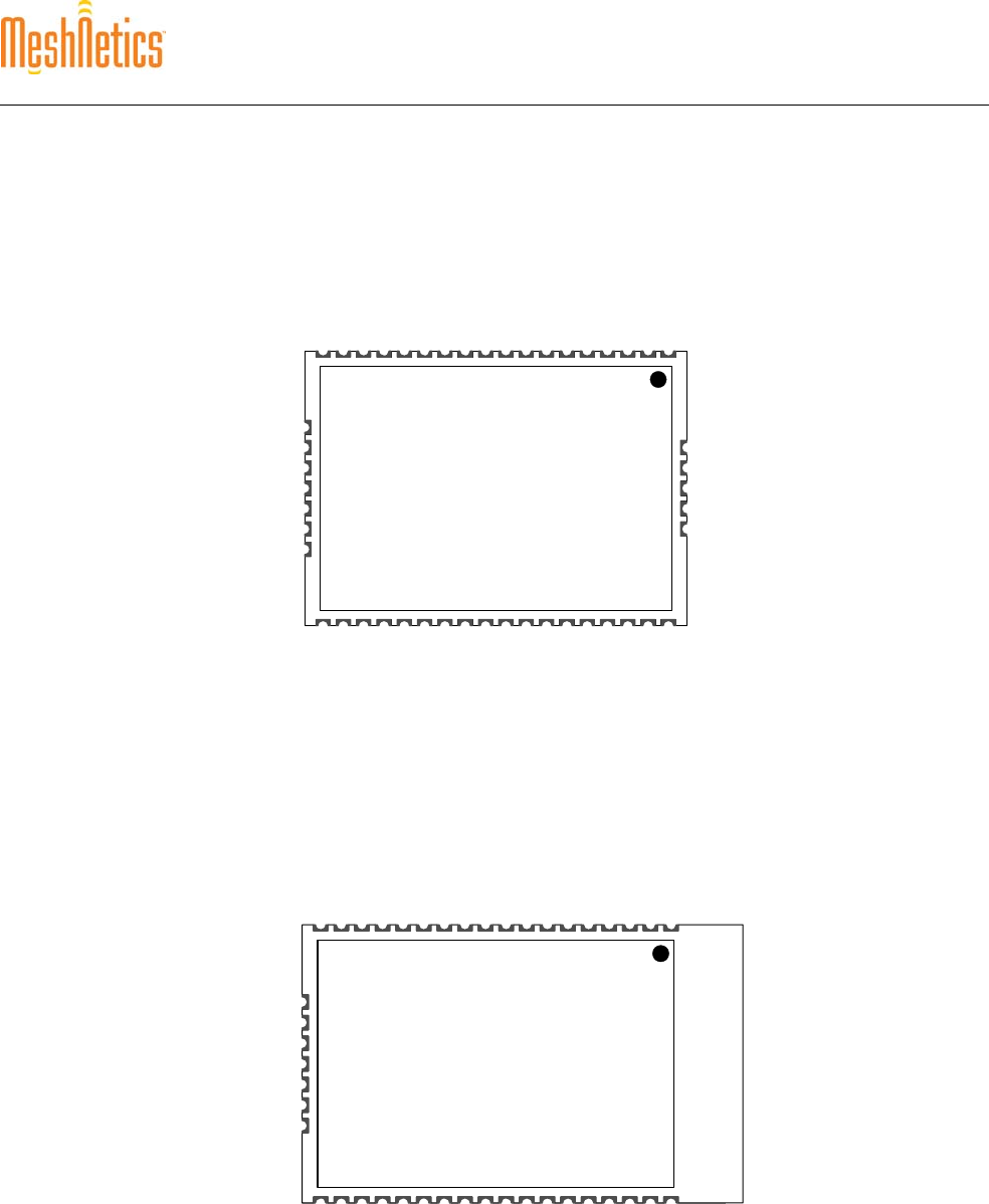
Physical/Environmental Characteristics and Outline
Paramete
r
V
alue Notes
Size 18.8 x 13.5 x 2.8 mm ZDM-A1281-B0
24.0 x 13.5 x 2.8 mm ZDM-A1281-A2
Wei
g
ht 1.3
g
ZDM-A1281-B0
1.5
g
ZDM-A1281-A2
Operating Temperature Range -20°C to +70°C -40°C to +85°C operational*
Operating Relative Humidity
Range no more than 80%
ZDM-A1281-B0 Mechanical Drawing
17,3±0,2
12,0±0,2
13,5±0,2
18,8±0,2
0,8-0.2
2,0±0,1
1,0 typ 0,7±0,1
118
1925
26 43
44 48
All dimensions are in millimeters
ZDM-A1281-A2 Mechanical Drawing
17,3±0,2
12,0±0,2
13,5±0,2
24,0±0,2
0,8-0.2
2,0±0,1
1,0 typ 0,7±0,1
118
1925
26 43
All dimensions are in millimeters
* Minor degradation of clock stability may occur
ZigBit™ OEM Modules Product Datasheet
© 2007 MeshNetics Page 8 of 22
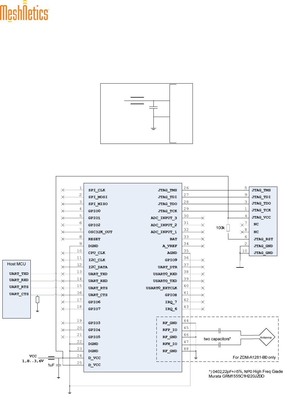
Pin Configuration
ZDM-A1281-B0 Pinout
118
1925
43
234567891011121314151617
26 3433323130292827 35 42414039383736
2021222324
4847464544
SPI_CLK
SPI_MOSI
SPI_MISO
GPIO0
GPIO1
GPIO2
OSC32K_OUT
RESET
DGND
CPU_CLK
I2C_CLK
I2C_DATA
UART_RXD
UART_TXD
GPIO6
GPIO7
IRQ_6
IRQ_7
GPIO8
USART0_EXTCLK
USART0_TXD
USART0_RXD
UART_DTR
GPIO9
AGND
A_VREF
BAT
ADC_INPUT_1
ADC_INPUT_2
ADC_INPUT_3
JTAG_TCK
JTAG_TDO
JTAG_TDI
JTAG_TMS
GPIO3
UART_CTS
UART_RTS
DGND
DGND
D_VCC
D_VCC
RF_GND
RFP_IO
RF_GND
RFN_IO
RF_GND
GPIO4
GPIO5
ZDM-A1281-A2 Pinout
118
1925
43
234567891011121314151617
26 3433323130292827 35 42414039383736
2021222324
SPI_CLK
SPI_MOSI
SPI_MISO
GPIO0
GPIO1
GPIO2
OSC32K_OUT
RESET
DGND
CPU_CLK
I2C_CLK
I2C_DATA
UART_RXD
UART_TXD
GPIO6
GPIO7
IRQ_6
IRQ_7
GPIO8
USART0_EXTCLK
USART0_TXD
USART0_RXD
UART_DTR
GPIO9
AGND
A_VREF
BAT
ADC_INPUT_1
ADC_INPUT_2
ADC_INPUT_3
JTAG_TCK
JTAG_TDO
JTAG_TDI
JTAG_TMS
GPIO3
UART_CTS
UART_RTS
DGND
DGND
D_VCC
D_VCC
GPIO4
GPIO5

ZigBit™ OEM Modules Product Datasheet
© 2007 MeshNetics Page 9 of 22
Pin Assignment Table
Conn
ector
Pin Pin Name Description I/O
Defaul
t State
after
power
on
Port
ATmega
1281V
ATmega
1281v
Datasheet
Reference*
Notes,
see list
below
1 SPI_CLK Reserved for stack operation O PB1 3
2 SPI_MOSI Reserved for stack operation O PB3 3
3 SPI_MISO Reserved for stack operation I/O PB2
Page 189
3
4 GPIO0 General purpose digital input/output
0 I/O tri-state PB5 1, 2, 3, 6
5 GPIO1 General purpose digital input/output
1 I/O tri-state PB6 1, 2, 3, 6
6 GPIO2 General purpose digital input/output
2 I/O tri-state PB7
Pages 78-
79, 86-87,
109
1, 2, 3, 6
7 OSC32K_OUT 32.768 kHz clock output. O PG3 Page 99 3, 4
8 RESET Reset input (active low). I RESET Page 56 3
9,
22,
23 DGND Digital ground
10 CPU_CLK
RF clock output. When module is in
active state, 4 MHz signal is present
on this line. While module is in the
sleeping state, clock generation is
stopped also.
O XTAL_In
3
11 I2C_CLK I2C serial clock output O tri-state PD0 1, 2, 3, 6
12 I2C_DATA I2C serial data input/output I/O tri-state PD1
Pages 233-
264,364 1, 2, 3, 6
13 UART_TXD UART receive pin I tri-state PD2 1, 2, 3, 6
14 UART_RXD UART transmit pin O tri-state PD3 Page 198 1, 2, 3, 6
15 UART_RTS RTS input (Request To Send) for
UART hardware flow control. Active
low. I tri-state PD4 1, 2, 3, 6
16 UART_CTS CTS output (Clear To Send) for
UART hardware flow control. Active
low. O tri-state PD5 1, 2, 3,
6, 7
17 GPIO6 General purpose digital input/output
6 I/O tri-state PD6 1, 2, 3, 6
18 GPIO7 General purpose digital input/output
7 I/O tri-state PD7
Pages 78-
79, 91, 110
1, 2, 3, 6
19 GPIO3 General purpose digital input/output
3 I/O tri-state PG0 1, 2, 3, 6
20 GPIO4 General purpose digital input/output
4 I/O tri-state PG1 1, 2, 3, 6
21 GPIO5 General purpose digital input/output
5 I/O tri-state PG2
Pages 79,
99, 111
1, 2, 3, 6
24,
25 D_VCC Digital supply voltage (Vcc) 8
26 JTAG_TMS JTAG test mode select I PF5 Pages 7, 1, 2, 3, 5

ZigBit™ OEM Modules Product Datasheet
© 2007 MeshNetics Page 10 of 22
Conn
ector
Pin Pin Name Description I/O
Defaul
t State
after
power
on
Port
ATmega
1281V
ATmega
1281v
Datasheet
Reference*
Notes,
see list
below
27 JTAG_TDI JTAG test data input I PF7 1, 2, 3, 5
28 JTAG_TDO JTAG test data output O PF6 1, 2, 3, 5
29 JTAG_TCK JTAG test clock I PF4
97, 288
1, 2, 3, 5
30 ADC_INPUT_3 ADC input channel 3 I tri-state PF3 1, 2, 6
31 ADC_INPUT_2 ADC input channel 2 I tri-state PF2 1, 2, 6
32 ADC_INPUT_1 ADC input channel 1 I tri-state PF1 1, 2, 6
33 BAT
ADC input channel 0. Used by the
stack for battery level
measurement. Nominal voltage is 1
V in respect to AGND.
I tri-state PF0
Pages 97,
266-287 1, 2, 6
34 A_VREF Output/Input reference voltage for
ADC I/O tri-state AREF Pages 274,
280
35 AGND Analog ground
36 GPIO9 General purpose digital input/output
9 I/O PG5 1, 2, 3, 6
37 UART_DTR DTR input (Data Terminal Ready)
for UART. Active low. I tri-state PE4 Pages 73,
93 1, 2, 3, 6
38 USART0_RXD UART/SPI receive pin I tri-state PE0 1, 2, 3, 6
39 USART0_TXD UART/SPI transmit pin O tri-state PE1 1, 2, 3, 6
40 USART0_EXT
CLK UART/SPI external clock I tri-state PE2
Pages 198,
224, 198-
232 1, 2, 3, 6
41 GPIO8 General purpose digital input/output
8 I/O tri-state PE3 1, 2, 3, 6
42 IRQ_7 Digital input interrupt request 7 I tri-state PE7 1, 2, 3, 6
43 IRQ_6 Digital input interrupt request 6 I tri-state PE6
Pages 73,
93-96
1, 2, 3, 6
44,
46,
48 RF_GND RF analog ground 9
45 RFP_IO Differential RF input/output. I/O 9
47 RFN_IO Differential RF input/output. I/O 9
Notes:
1. *Most of pins can be configured for general purpose I/O or for some alternative functions as described in
details in the ATmega1281V Datasheet [1].
2. GPIO pins can be programmed either for output, or input with/without pull-up resistors. Output pin drivers
are strong enough to drive LED displays directly (refer to figures on pages 387-388, [1]).
3. All digital pins are provided with protection diodes to D_VCC and DGND
4. It is strongly recommended to avoid assigning an alternative function for OSC32K_OUT pin because it is
used by eZeeNet Framework. However, this signal can be used if another peripheral or host processor
requires 32.768 kHz clock, otherwise this pin can be disconnected.
5. Normally, JTAG_TMS, JTAG_TDI, JTAG_TDO, JTAG_TCK pins are used for on-chip debugging and flash
burning. They can be used for A/D conversion if JTAGEN fuse is disabled.
6. eZeeNet software can configure as general-purpose I/O lines the following pins: GPIO0, GPIO1, GPIO2,
GPIO3, GPIO4, GPIO5, GPIO6, GPIO7, GPIO8, GPIO9, I2C_CLK, I2C_DATA, UART_TXD, UART_RXD,
UART_RTS, UART_CTS, ADC_INPUT_3, ADC_INPUT_2, ADC_INPUT_1, BAT, UART_DTR,
USART0_RXD, USART0_TXD, USART0_EXTCLK, IRQ_7, IRQ_6. Additionally, four JTAG lines could be
ZigBit™ OEM Modules Product Datasheet
© 2007 MeshNetics Page 11 of 22
programmed with software as GPIO as well, but this requires changing the fuse bits and will disable JTAG
debugging.
7. CTS pin can be configured by eZeeNet to indicate sleep/active condition of the module thus providing
mechanism for power management of host processor. If such functionality is needed, it is recommended to
connect external pull-down resistor to this pin to prevent undesirable transients during module reset
process.
8. It is recommended to use ferrite bead and 1 µF capacitor located closely to the power supply pin, as shown
below.
D_VCC
DGND
1,8...3,6 V
9. Pins 44 through 48 are not present on the module with chip antennas
Typical schematics

ZigBit™ OEM Modules Product Datasheet
© 2007 MeshNetics Page 12 of 22
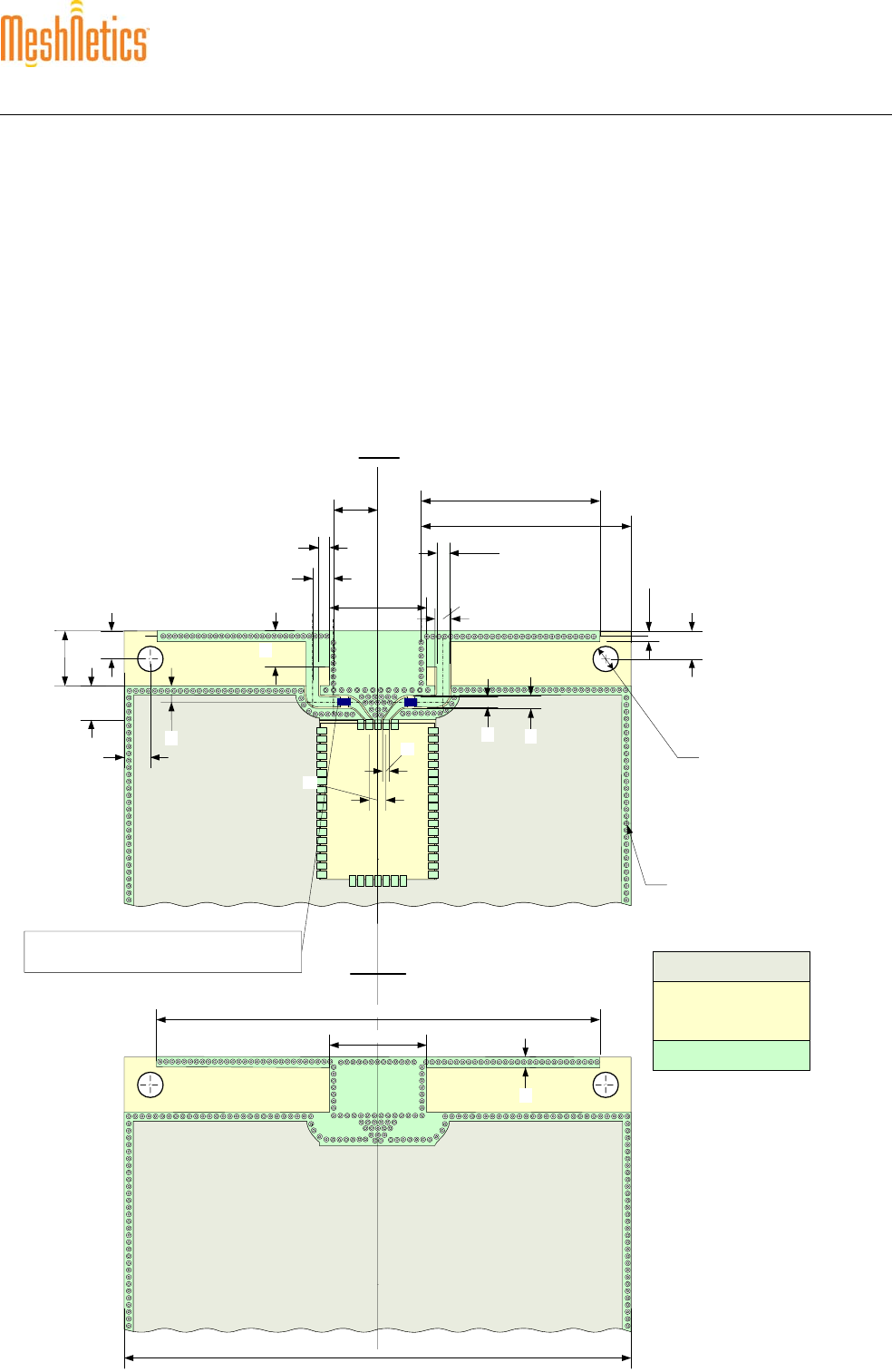
Mounting Information
ZDM-A1281-B0 PCB Recommended Layout, Top View
19,7
14,4
0,8
1,2
118
1925
4326
4844
All dimensions are in millimeters
1,0
ZDM-A1281-A2 PCB Recommended Layout, Top View
14,4
0,8
1,2
118
1925
4326
All dimensions are in millimeters
0,5
0,9
3,8
1,0
24,0
The above diagrams show the recommended PCB layout for ZigBit module. No via-holes and no wires are allowed
on the PCB upper layer in the area occupied by the module. As a critical requirement, RF_GND pins should be
grounded via several holes located very close to pins thus minimizing inductance and preventing mismatch and
losses.
ZigBit™ OEM Modules Product Datasheet
© 2007 MeshNetics Page 13 of 22
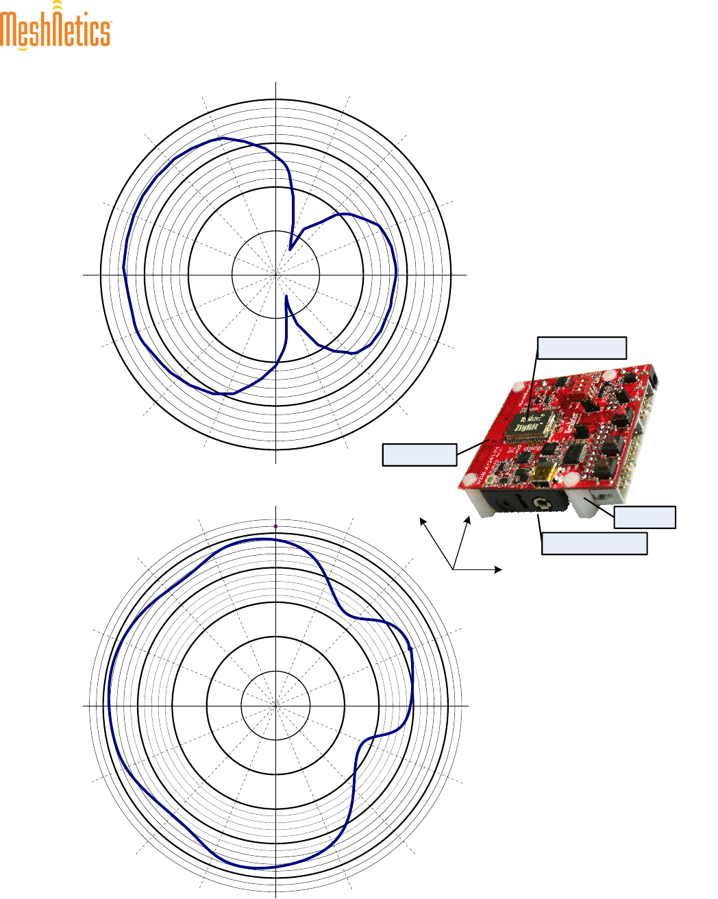
Sample Antenna Reference Designs
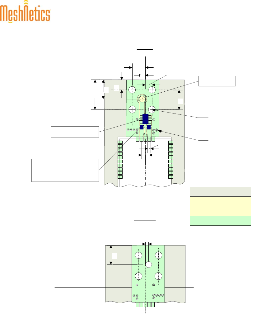
The following reference antenna design shows an example that can serve as a basis for further optimization.
The symmetric dipole antenna shown below has been tuned for a particular case, so the cut-and-paste approach
would not necessarily ensure an optimum performance because of multiple factors affecting the antenna matching
and pattern (for instance, the board material and thickness, shields, the material of enclosure, the board
neighborhood, other components located next to antenna and so on). As a general recommendation, metal
enclosures or setting high profile components closely to antenna should be avoided. Using low profile enclosures
can, furthermore, cause antenna tuning. The holes shown located around the board eliminate the undesirable
antenna pattern distortions which might be induced by radiation from the board edges. The ZigBit module should not
be placed next to components causing undesirable interference in its operating frequency band or adjacent bands,
such as GSM, CDMA, WiFi, and Bluetooth.
PCB Layout: Symmetric Dipole Antenna recommended for ZDM-A1281-B0
ZigBit
Module
ZigBit
Module
60,0
4,0
1,2
6,5
25,0
3,3
3,3
No metallization, wires,
through holes allowed
Metallization
Components area
11,5
11,5
52,5
1,2
Top side
Bottom side
Material: FR-4. thickness 1.6 mm
Metallization: 35 um
Coating: HASL, solder mask
All dimensions are in millimeters
2 through holes O3,0
1,8
4,6
1,9
3,0
Metallized through holes O0.3~0.4
Recommended step 1 mm
1,2
21,0
2,6
1,4
5,2
1.8
1,2
0,7
2,0
Two capacitors 0402,22pF+/-5%, NP0 High Freq Grade
Murata GRM1555C1H220JZ0D
ZigBit™ OEM Modules Product Datasheet
© 2007 MeshNetics Page 14 of 22
5
4
3
2
1
0
-1
-2
-3
-4
-5
-
1
0
0º
22,5º
45º
67,5º
90º
112,5º
135º
157,5º
180º
202,5º
225º
247,5º
270º
292,5º
315º
337,5º ZDM-A1281-B0
PCB Antenna
Battery compartment
X
Y
X
ZY
2
1
0
67,5º
90º
112,5º
270º
Z
-1
-2
-3
-4
-5
0º
22,5º
135º
157,5º
180º
202,5º
225º
247,5º 292,5º
315º
337,5º
-6
-7
-8
-9
-10
-15
-20
45º
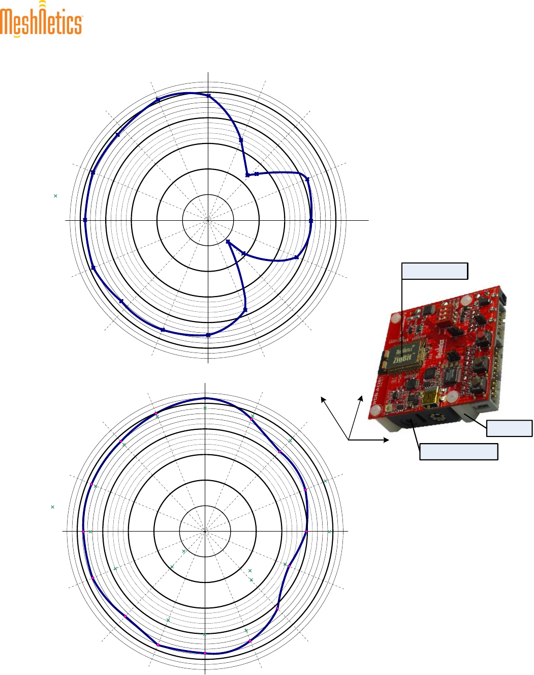
ZDM-A1281-B0 Pattern:
Symmetric Dipole Antenna
(horizontal plane)
ZDM-A1281-B0 Pattern
(vertical plane)
Nylon leg
ZigBit™ OEM Modules Product Datasheet
© 2007 MeshNetics Page 15 of 22
2
1
0
67,5º
90º
112,5º
270º
Z
2
1
0
-1
-2
-3
-4
-5
0º
22,5º
45º
67,5º
90º
112,5º
135º
157,5º
180º
202,5º
225º
247,5º
270º
292,5º
315º
337,5º
-6
-7
-8
-9
-10
-15
-20
X
Y
Battery compartment
ZDM-A1281-A2
-1
-2
-3
-4
-5
0º
22,5º
135º
157,5º
180º
202,5º
225º
247,5º 292,5º
315º
337,5º
-6
-7
-8
-9
-10
-15
-20
X
45º
ZDM-A1281-A2 Pattern
(horizontal plane)
ZDM-A1281-A2 Pattern
(vertical plane)
X
ZY
Nylon leg
Note: The presented antenna patterns were observed using PCB enhanced with legs made of original nylon.
ZigBit™ OEM Modules Product Datasheet
© 2007 MeshNetics Page 16 of 22
Normally chip antennas are more tolerant of board and enclosure materials, and ZigBit module neighborhood;
however, general recommendations for board design for the PCB antenna version still apply.
The board should be designed such that it prevents propagation of microwave field inside the board material itself.
High frequency electromagnetic field may penetrate the board and radiate from the edges of the board causing
undesirable pattern distortions. To eliminate this effect, it is often enough to surround the board with metallized
holes connected to module ground.
Since the module with chip antenna is tuned for installation on FR-4 board with thickness 1.6 mm, the performance
is guaranteed only if the board is designed according to the diagram below. Deviations from this design may change
the performance.
Recommended Layout for Chip Antenna Module (ZDM-A1281-A2)
ZigBit
Module
ZigBit
Module
6,5
Metallized through holes O0.3~0.4
Recommended step 1 mm
60,0
2 through holes O3,0
3,5
No metallization, wires,
through holes allowed
Metallization
Components area
Top side
Bottom side
Material: FR-4. thickness 1.6 mm
Metallization: 35 um
Coating: HASL, solder mask
All dimensions are in millimeters
3,5
ZigBit™ OEM Modules Product Datasheet
© 2007 MeshNetics Page 17 of 22
Recommended PCB Layout for 50 Ohm External Antenna (ZDM-A1281-B0)
Material: FR-4. thickness 1.6 mm
Metallization: 35 um
Coating: HASL, solder mask
Detailed dimensions: see datasheets
for Balun and SMA-Connector
No metallization, wires,
through holes allowed
Metallization
Components area
Top side
Bottom side
All dimensions are in millimeters
2,0
7,5
2,6
0,7
1,7
5,1
Balun TDK’s HHM1520
SMA-Connector
Metallized through holes O0,3~0,4
Recommended step 1 mm
0,9
3,4
5,0
0,9
5,0
4 through holes O1,9
Two capacitors 0402,22pF+/-5%,
NP0 High Freq Grade
Murata GRM1555C1H220JZ0D
In case an external antenna or a 50 Ohm unbalanced antenna is required, they can be easily interfaced to ZigBit
module ZDM-A1281-B0 by using 2:1 balun as shown above. This recommended sample demonstrates how to use
low-profile Murata connector. It can be simply replaced with 50 Ohm microstrip line as shown in TDK’s HHM1520
Balun Datasheet [6].

ZigBit™ OEM Modules Product Datasheet
© 2007 MeshNetics Page 18 of 22
Agency Certifications
UNITED STATES (FCC)
This equipment complies with Part 15 of the FCC rules and regulations.
To fulfill FCC Certification requirements, an OEM manufacturer must comply with the following
regulations:
1. The modular transmitter must be labelled with its own FCC ID number, and, if the FCC ID is not
visible when the module is installed inside another device, then the outside of the device into
which the module is installed must also display a label referring to the enclosed module. This
exterior label can use wording such as the following:
Example of label required for OEM product containing ZDM-A1281-A2 module
Contains FCC ID: U6TZIGBIT-A2
The enclosed device complies with Part 15 of the FCC Rules. Operation is subject to the
following two conditions: (i.) this device may not cause harmful interference and (ii.) this device
must accept any interference received, including interference that may cause undesired
operation.
Example of label required for OEM product containing ZDM-A1281-B0 module
Contains FCC ID: U6TZIGBIT-B0
The enclosed device complies with Part 15 of the FCC Rules. Operation is subject to the
following two conditions: (i.) this device may not cause harmful interference and (ii.) this device
must accept any interference received, including interference that may cause undesired
operation.
Any similar wording that expresses the same meaning may be used.
2. To be used with the ZDM-A1281-B0 module, the external antennas have been tested and
approved which are specified in Approved Antenna List herebelow. The ZDM-A1281-B0
Module may be integrated with other custom design antennas which OEM installer must
authorize following the FCC 15.21 requirements.
WARNING: The Original Equipment Manufacturer (OEM) must ensure that the OEM modular transmitter must be
labeled with its own FCC ID number. This includes a clearly visible label on the outside of the final
product enclosure that displays the contents shown below. If the FCC ID is not visible when the
equipment is installed inside another device, then the outside of the device into which the equipment is
installed must also display a label referring to the enclosed equipment.
IMPORTANT: This equipment complies with Part 15 of the FCC Rules. Operation is subject to the following two
conditions: (1) this device may not cause harmful interference, and (2) this device must accept any
interference received, including interference that may cause undesired operation (FCC 15.19).
The internal / external antenna(s) used for this mobile transmitter must provide a separation distance of
at least 20 cm from all persons and must not be co-located or operating in conjunction with any other
antenna or transmitter.
Installers must be provided with antenna installation instructions and transmitter operating conditions for
satisfying RF exposure compliance. This device is approved as a mobile device with respect to RF
exposure compliance, and may only be marketed to OEM installers. Use in portable exposure conditions
(FCC 2.1093) requires separate equipment authorization.
IMPORTANT: Modifications not expressly approved by this company could void the user's authority to operate this
equipment (FCC section 15.21).
IMPORTANT: This equipment has been tested and found to comply with the limits for a Class A digital device,
pursuant to Part 15 of the FCC Rules. These limits are designed to provide reasonable protection
against harmful interference when the equipment is operated in a commercial environment. This
equipment generates, uses, and can radiate radio frequency energy and, if not installed and used in
accordance with the instruction manual, may cause harmful interference to radio communications.
Operation of this equipment in a residential area is likely to cause harmful interference in which case the
user will be required to correct the interference at his own expense (FCC section 15.105).
ZigBit™ OEM Modules Product Datasheet
© 2007 MeshNetics Page 19 of 22
CANADA (IC)
Equipment is subject to certification under the applicable RSSs, shall be permanently labelled on each
item, or as an inseparable combination. The label must contain the following information for full
compliance:
For ZDM-A1281-A2 module:
Certification Number: IC: 7036A-ZIGBITA2
Manufacturer’s Name, Trade Name or Brand Name: ZIGBIT
Model Name: ZDM-A1281-A2
For ZDM-A1281-B0 module:
Certification Number: IC: 7036A-ZIGBITB0
Manufacturer’s Name, Trade Name or Brand Name: ZIGBIT
Model Name: ZDM-A1281-B0
IMPORTANT: This equipment for which a certificate has been issued is not considered certified if it is not properly
labelled. The information on the Canadian label can be combined with the manufacturer’s other labelling
requirements
IMPORTANT: Operation is subject to the following two conditions: (1) this device may not cause harmful
interference, and (2) this device must accept any interference received, including interference that may
cause undesired operation.
IMPORTANT: To reduce potential radio interference to other users, the antenna type and its gain should be so
chosen that the equivalent isotropically radiated power (e.i.r.p.) is not more than that permitted for
successful communication.
IMPORTANT: The installer of this radio equipment must ensure that the antenna is located or pointed such that it
does not emit RF field in excess of Health Canada limits for the general population. Consult Safety Code
6, obtainable from Health Canada’s website www.hc-sc.gc.ca/rpb.
EUROPEAN UNION (ETSI)
The ZDM-A1281-A2 and ZDM-A1281-B0 Modules has been certified for use in European Union
countries.
If the ZDM-A1281-A2 and ZDM-A1281-B0 Modules are incorporated into a product, the manufacturer
must ensure compliance of the final product to the European harmonized EMC and low-voltage/safety
standards. A Declaration of Conformity must be issued for each of these standards and kept on file as
described in Annex II of the R&TTE Directive.
Furthermore, the manufacturer must maintain a copy of the ZDM-A1281-A2 and ZDM-A1281-B0
Modules documentation and ensure the final product does not exceed the specified power ratings,
antenna specifications, and/or installation requirements as specified in the user manual. If any of these
specifications are exceeded in the final product, a submission must be made to a notified body for
compliance testing to all required standards.
IMPORTANT: The 'CE' marking must be affixed to a visible location on the OEM product. The CE mark shall consist
of the initials "CE" taking the following form:
• If the CE marking is reduced or enlarged, the proportions given in the above graduated drawing
must be respected.
• The CE marking must have a height of at least 5mm except where this is not possible on
account of the nature of the apparatus.
• The CE marking must be affixed visibly, legibly, and indelibly.
More detailed information about CE marking requirements you can find at “DIRECTIVE 1999/5/EC OF
THE EUROPEAN PARLIAMENT AND OF THE COUNCIL” on 9 March 1999 at section 12.
Certification Approved Antennas list is presented in Approved Antenna List below.

ZigBit™ OEM Modules Product Datasheet
© 2007 MeshNetics Page 20 of 22
Approved Antenna List
ZDM-A1281-A2 Module has only possibility to work with installed chip-antenna. The design of the chip-
antenna is fully tested and satisfies all the legislation mentioned above.
ZDM-A1281-B0 Module has been tested and approved for use with the antennas listed in the table
below. The ZDM-A1281-B0 Module may be integrated with other custom design antennas which OEM
installer must authorize following the respective legislation requirements.
Part Number Manufacturer & Description Gain, dBi Min. Separation, cm
2010B4844-01 Antenova Titanis, swivel antenna (1/4
wave antenna) with SMA connector,
frequency range 2.4-2.5 GHz
4.1 20
17010.10 WiMo, swivel antenna (1/2 wave
antenna) with SMA connector,
frequency range 2.35-2.5 GHz
2.1 20
Technical Support
Tel: +7 (495) 725 8125
E-mail: support@meshnetics.com
Development Support
• Easy-to-use Evaluation and Development Kits are available.
• Source code samples and RF reference designs are available to qualified customers.
• MeshNetics runs the ZigBit Priority Support Program to facilitate faster delivery of ZigBit-based applications
to the market. The qualified customers enjoy priority samples policy, direct access to MeshNetics RF
experts, 802.15.4 MAC-, eZeeNet stack- and Gateways- development teams, dedicated FAE for application
consulting and other technical resources to accelerate the development of ZigBit-based products and
applications. To qualify for the Program, please contact us at zigbit@meshnetics.com for more details.
Ordering Information
You can contact MeshNetics for additional modules, the Evaluation Kit or the Developer’s Kit to build your custom
network. Please e-mail us at zigbit@meshnetics.com, or visit us online at www.meshnetics.com/contacts.
Please specify the product part number and description when ordering.
Part Number Description
ZDM-A1281-B0 2.4 GHz IEEE802.15.4/ZigBee OEM Module w/ Balanced RF Port
ZDM-A1281-A2 2.4 GHz IEEE802.15.4/ZigBee OEM Module with chip antennas

ZigBit™ OEM Modules Product Datasheet
© 2007 MeshNetics Page 21 of 22
Related Documents
[1] Atmel 8-bit AVR Microcontroller with 64K/128K/256K Bytes In-System Programmable Flash.
2549F-AVR-04/06
[2] Atmel Low-Power Transceiver for ZigBee Applications. AT86RF230 Target Specification.
5131A-ZIGB-08/15/05
[3] IEEE Std 802.15.4-2003 IEEE Standard for Information technology – Part 15.4 Wireless Medium Access
Control (MAC) and Physical Layer (PHY) Specifications for Low-Rate Wireless Personal Area Networks
(LR-WPANs)
[4] ZigBee Specification. ZigBee Document 053474r14, November 03, 2006
[5] eZeeNet™ IEEE802.15.4/ZigBee Software. Product Datasheet. MeshNetics Doc. M-251~02
[6] Multilayer Baluns, HHM Series. HHM1520 For Bluetooth & IEEE802.11b/g,
www.tdk.co.jp/tefe02/e8balun_hhm.pdf
Disclaimer
MeshNetics believes that all information is correct and accurate at the time of issue. MeshNetics reserves the right
to make changes to this product without prior notice. Please visit MeshNetics website for the latest available version.
MeshNetics does not assume any responsibility for the use of the described product or convey any license under its
patent rights.
Trademarks
MeshNetics®, ZigBit, eZeeNet, ZigBeeNet, SensiLink, LuxLabs, Luxoft Labs, and MeshNetics, Luxoft Labs and
ZigBit logos are trademarks of LuxLabs Ltd.
All other product names, trade names, trademarks, logos or service names are the property of their respective
owners.
© 2007 MeshNetics. All rights reserved.
No part of the contents of this manual may be transmitted or reproduced in any form or by any means without the
written permission of MeshNetics.
Contact Information
MeshNetics
9 Dmitrovskoye Shosse
Moscow 127434, Russia
Tel: +7 (495) 725 8125
Fax: +7 (495) 725 8116
E-mail: zigbit@meshnetics.com
Website: www.meshnetics.com
Office hours: 8:00am – 5:00pm (Central European Time)

ZigBit™ OEM Modules Product Datasheet
© 2007 MeshNetics Page 22 of 22