M2Communication MA903A1 Wireless AP Module_9 series User Manual MA903A1 FCC 20151021
M2Communication Inc. Wireless AP Module_9 series MA903A1 FCC 20151021
OEM Manual
MA903A1
Wireless AP Module_9 series
Copyright © by M
2
Communcation, Inc. All rights reserved. This document is the sole and exclusive
property of M2Communication, Inc. Not to be distributed or divulged without prior written agreement.
Feature Highlights
Low supply operation: 2.4V –
3.6V
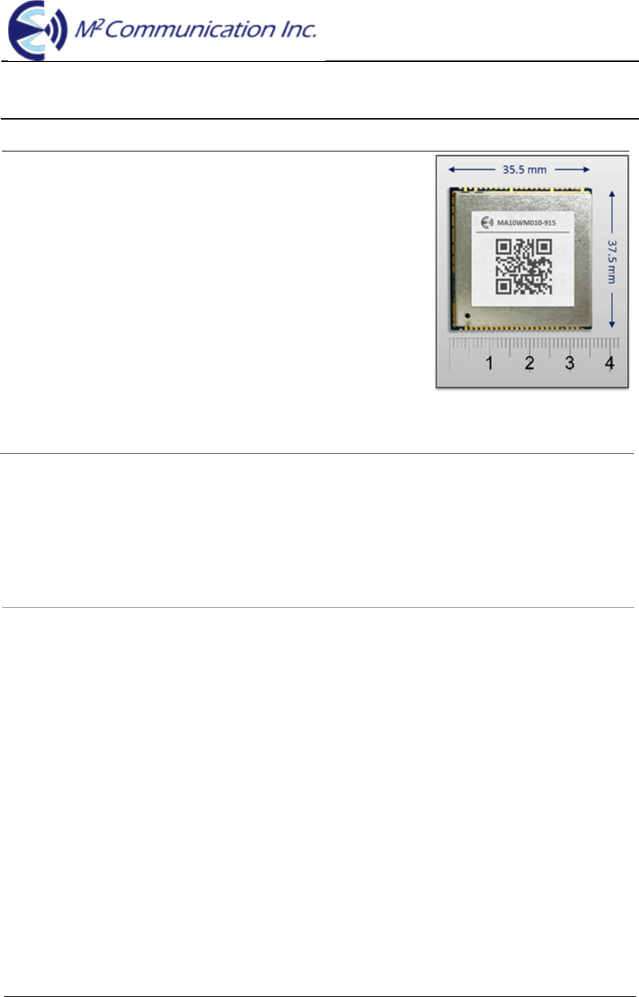
Compact size: 35.5mm x 37.5
mm, ideal for embedded system
integration such as access point
Low-power consumption
Using M2C patented Platanus™
platform for smart-networking
application
ARM Cortex-M0 up to 32MHz
clock rate, with embedded 128
KB flash memory and 1MB
SRAM
Frequency range: 903~927MHz
Data bandwidth: up to 500kbps
High receiver sensitivity: -96dBm
at 500kbps
Integrated power amplifier up to
11dBm
Pre-matched RF front-end,
reducing design hassles
Support UART and GPIOs as
interface with other LAN modules
in the embedded system
Supports 128-node “star” and
16000-node “tree” network
infrastructure.
Applications
Comply with FCC Part 15C
Innovative turn-key solution
for ultra-low power wireless
link
Remote control systems
Wireless sub-metering (plug)
Home automation
Wireless sensor network
Telemedicine service
Wireless lighting control
Smart rack for logistics
system
Descriptions
Overview
MA903A1 is an easy-to-integrate Access Point embedded module for hosting ultra-low-power
wireless-link application. With state-of-the-art PlatanusTM protocol and networking kit, large network
(up to 16000 nodes) can be easily formed. Equipped with ISM-band RF operated at 868MHz/915MHz
bands and popular ARM 32-bit MCU along with embedded flash memory and SRAM, MA903A1 is an
ideal embedded solution for system integrator to develop wireless applications with no worry about
design hassles, both wireless and networking.
Easy to Integrate and Use
Designed as the embedded module, MA903A1 has only the board area of 35.5mm x 37.5mm,
compact enough for most embedded system design. A pre-matched 50 ohm port is ready to be used
with on-board or external antenna. The RF matched network is calibrated to optimize the RF
performance when the module is shipped, saving the design hassles for application designers.
There are total 50 stamp pads on MA903A1 with multiple digital interfaces: UART, GPIOs, and
JTAGS. This brings the design flexibility to end applications that MA903A1 is easy to interface with
other LAN modules. Through the robust wireless link, controlled/collected information from End Device
(ME10WM010) can be easily sent to the upper application layers and devices.
Datasheet v1.0
MA903A1
2014/01 Copyright © by M
2
Communication Inc. Page 2 of 22
Ready
-
to
-
go
S
ub
-
GHz
R
adio
L
ink
with
Excellent Reliability
The wireless link utilizes the sub-GHz radio band, requiring no special licenses (free-ISM) and
certification. MA903A1 comply with the ETSI EN 300 220 and FCC part 15 regulations. Compared to
the crowded 2.4GHz band, sub-GHz radio link, given the similar power level, allows better distance
and penetration especially in the hostile indoor environment. In particular, with WiFi and Bluetooth
crowding the 2.4GHz band these days, MA903A1 is immune from all 2.4GHz interference and delivers
the reliable wireless link. With the data rate of 500kbps in 2FSK, the bandwidth use efficiency is 16x
better than 2.4GHz Zigbee (2MHz). MA903A1 can deliver the link budget up to 107dBm without
adding external components. The Line-of-Sight (LOS) link distance is over 300 meters*.
* tested with 63-byte payload with PER of 1%. This may be variable depending on test environment
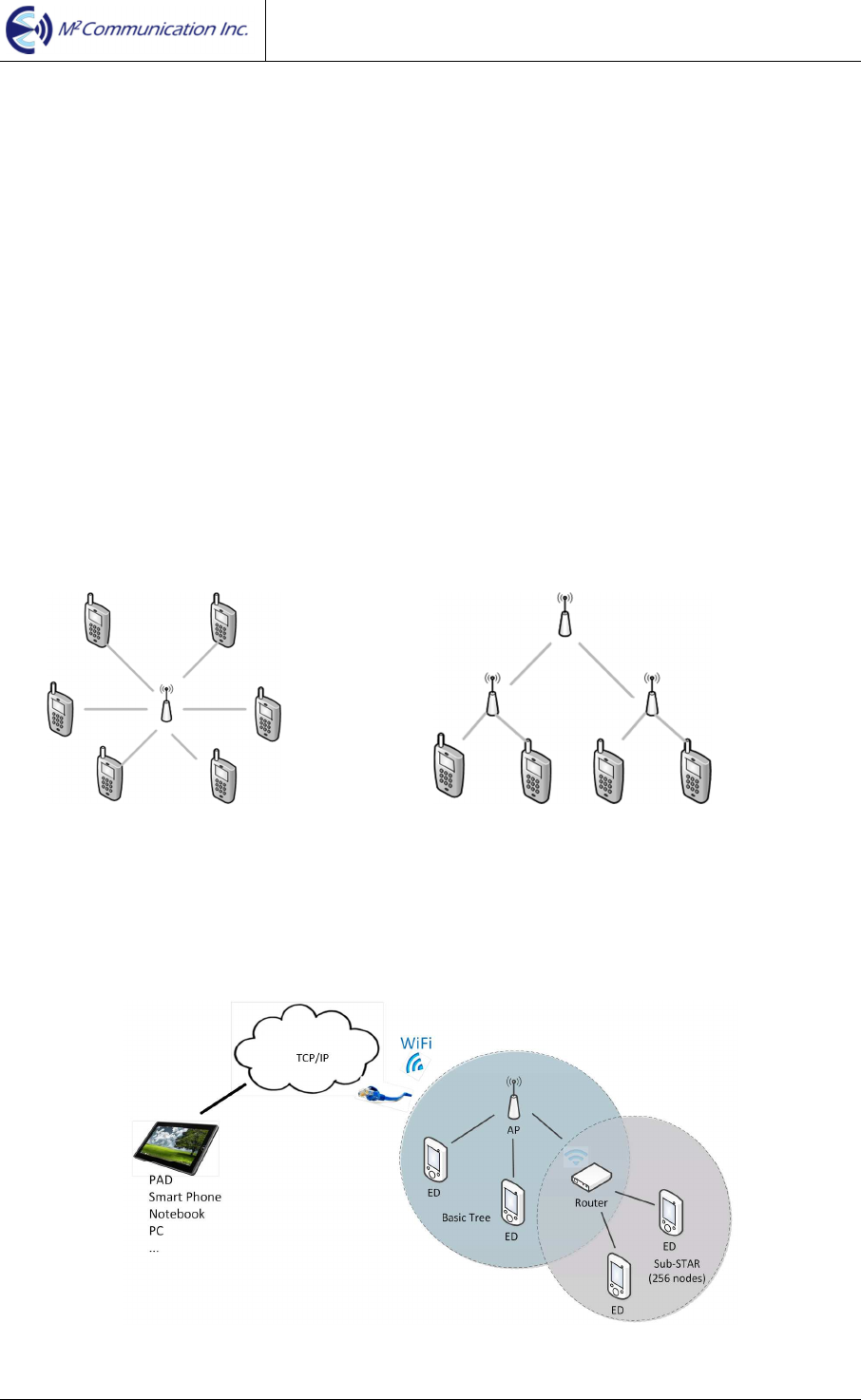
Robust Two-way Networking
MA903A1 uses a built-in protocol PlatanusTM to support “two-way” networking, saving the SI’s design
headache of linking large amounts of wireless nodes. Used with ME10WM010 (End Device),
MA903A1 can support two types of network hierarchies: STAR and TREE (as shown below). When
MA903A1 is configured in STAR networking, up to 128 nodes can be supported. When MA903A1 is
configured in TREE network, up to 16000 nodes can be supported. Asymmetrical downlink and uplink
are supported to balance between network reliability and response time, and the programmable
network parameters can be used to optimize for each use scenario.
Figure 1. STAR configuration Figure2. TREE configuration
Upper Layer Connectivity
MA903A1 is shipped with the UART interface and the managing software library. Thus the upper-layer
devices, such as TCP/IP gateway, can easily access MA903A1 in the network, as the Access Point to
the private network, to exchange data “interactively” via the Ethernet or WiFi. This makes the cloud-
based application developer easy to hook up with the privately-own network when building with
MA903A1.
Figure 3. Network Structure
Datasheet v1.0
MA903A1
2014/01 Copyright © by M
2
Communication Inc. Page 3 of 22
Ideal Platform for Low
-
power Application Development
MA903A1 is powered by ARM Cortex MCU with clock up to 32MHz with embedded 128K-Byte flash
and 1M-Byte SRAM, to support built-in PlatanusTM networking library from M2C and for peripherals.
For details, please refer to the associated documentation.
Using PlatanusTM protocol with M2C MA903A1 (Access Point) and/or MR1001 (Router), the formed
network can achieve ultra-low power consumption for battery-friendly applications. The network acts in
the cellular-like behavior, with sleep time configurable from 5 seconds up to 90 seconds. Details of
power consumption can be referred to the datasheet of ME10WM010.
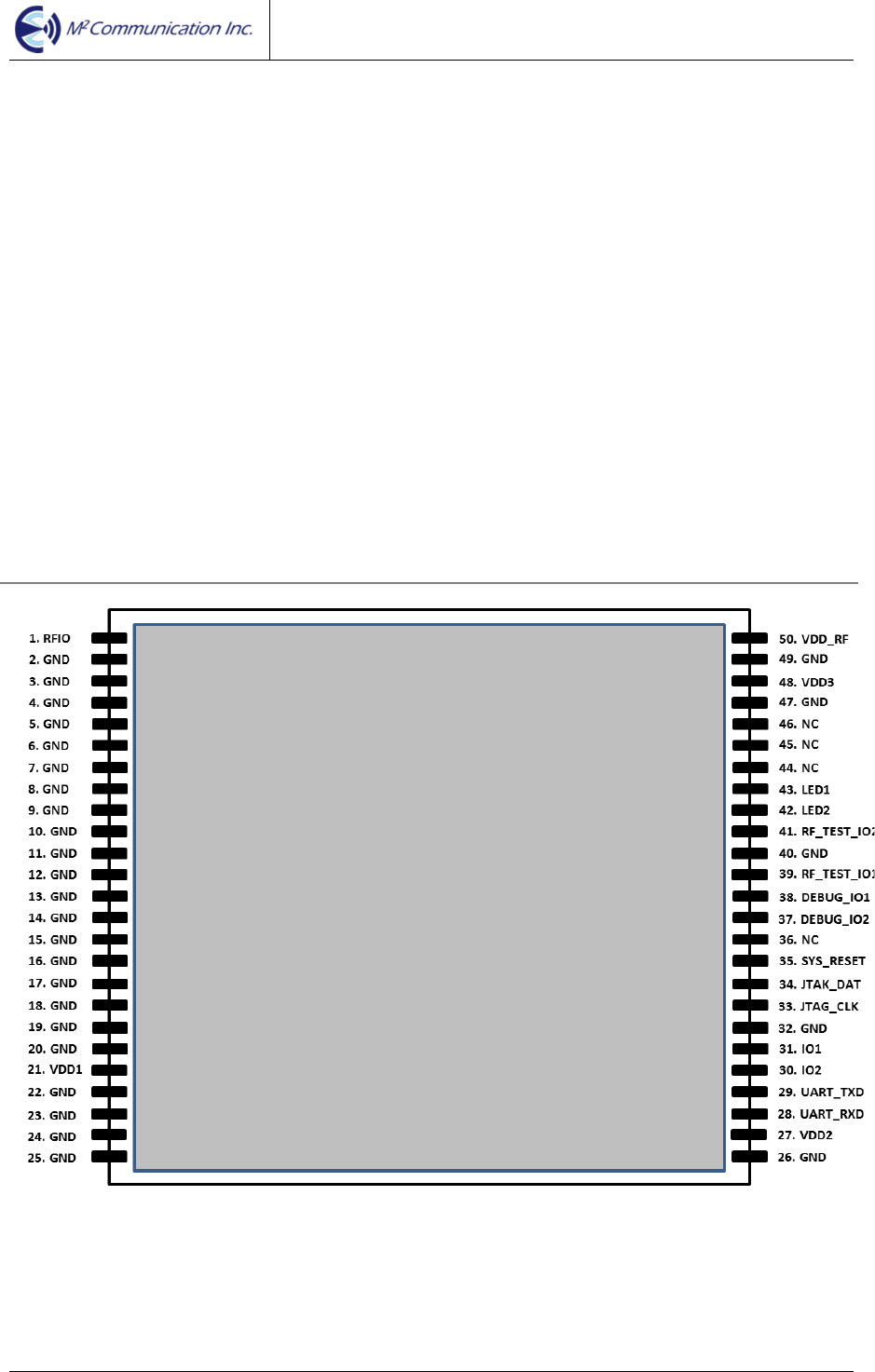
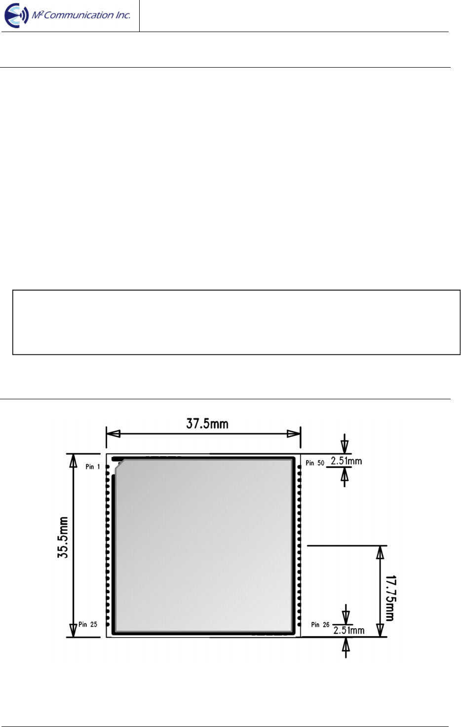
Pin Diagram & Components Placement
Figure4. Pin diagram
Datasheet v1.0
MA903A1
2014/01 Copyright © by M
2
Communication Inc. Page 4 of 22
Figure5. Pin diagram

Datasheet v1.0
MA903A1
2014/01 Copyright © by M
2
Communication Inc. Page 5 of 22
Table of Contents
1 Electrical Characteristics ................................................................................... 6
2 Pin Out ................................................................................................................. 9
3 Memory .............................................................................................................. 10
4 Serial Interfaces ................................................................................................ 10
4.1 General-purpose I/O (GPIO) .................................................................................................... 10
4.2 UART ........................................................................................................................................ 10
5 How to Use MA903A1 to Design ...................................................................... 11
5.1 50ohm RF Trace Calculation .................................................................................................... 11
5.2 PCB Design .............................................................................................................................. 12
5.3 PCB Layout Recommend ......................................................................................................... 14
5.4 PCB Layout Guide .................................................................................................................... 14
6 Available Antenna List ..................................................................................... 15
7 Regulation Approval......................................................................................... 19
8 Recommended PCB Footprint ......................................................................... 19
9 Contact Information.......................................................................................... 20
10 Ordering Information ..................................................................................... 20
Datasheet v1.0
MA903A1
2014/01 Copyright © by M
2
Communication Inc. Page 6 of 22
1 Electrical Characteristics
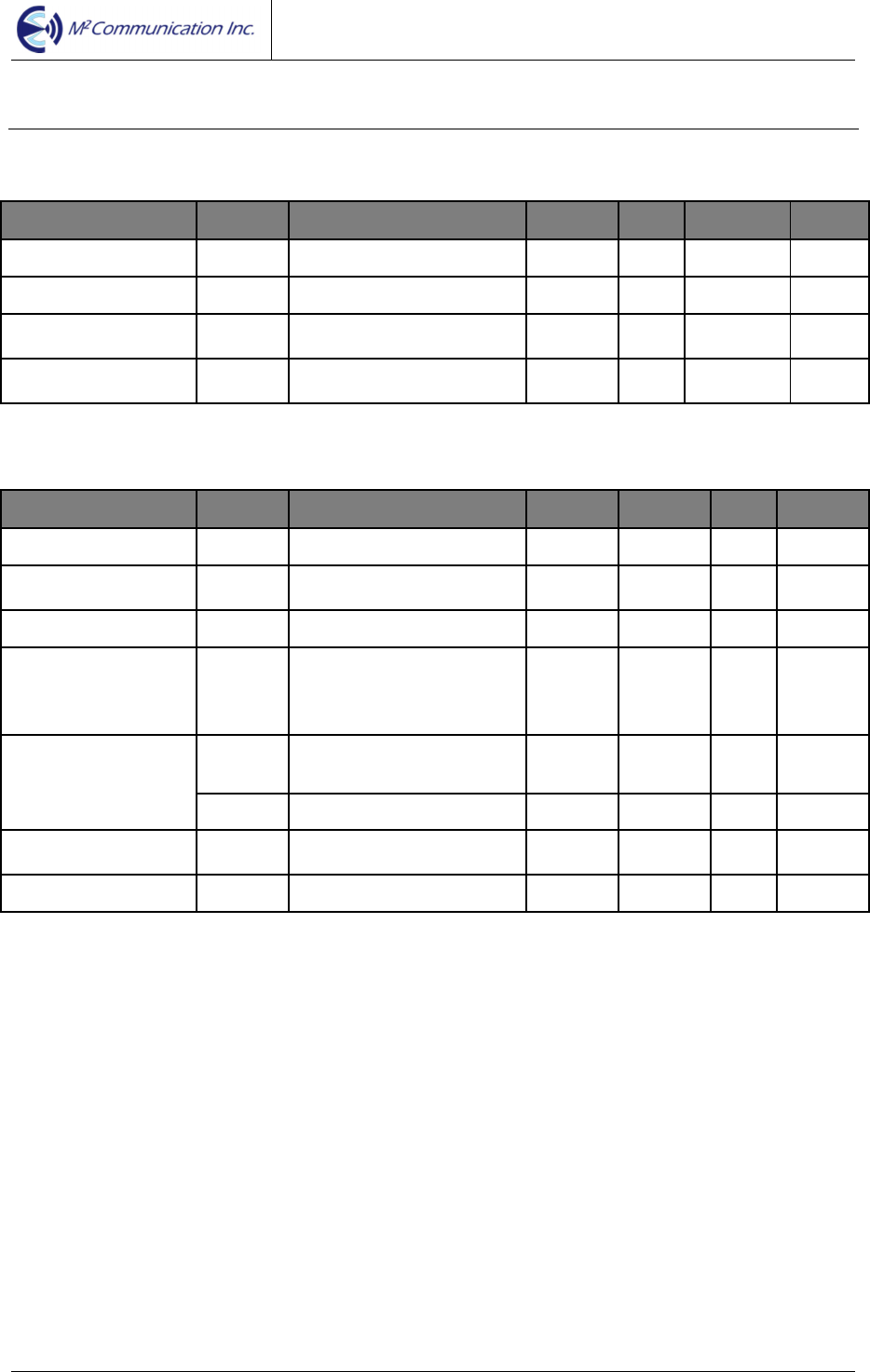
Table 1. Absolute Maximum Rating
Parameter Symbol
Condition Min Typ
Max Unit
Supply Voltage Vdd VCC to GND -0.3 3.6 Volt
Voltage on I/O Pin VIO -0.3 Vcc + 0.3
Volt
Temperature Range
for Storage Tsto -10 +85 oC
Operation
Temperature Topt -10 +45 oC
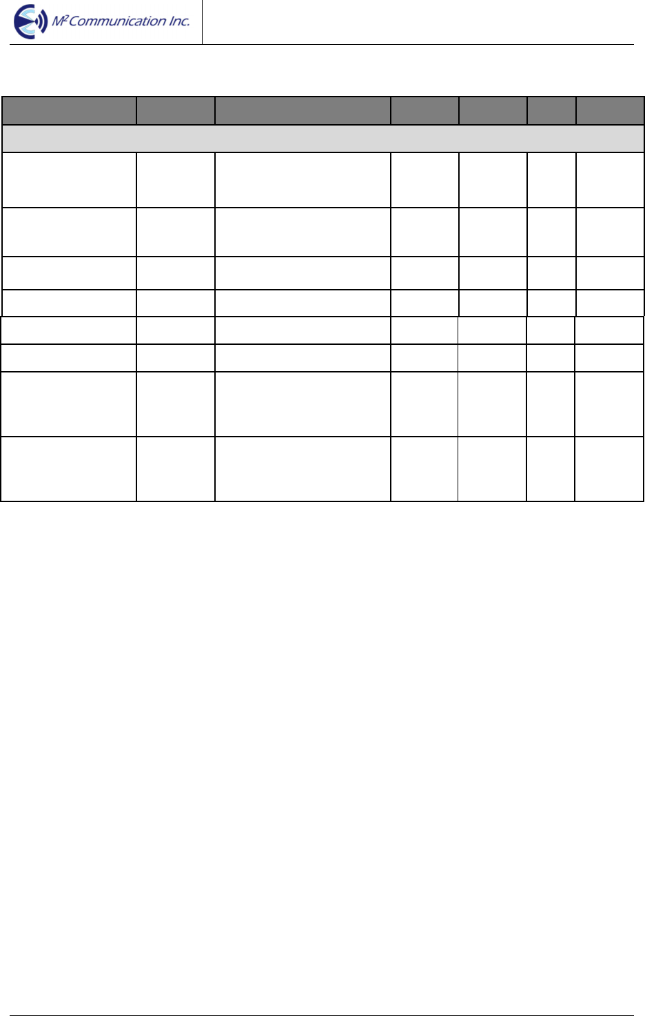
Table 2. DC Characteristics
Parameter Symbol
Condition Min Typ Max
Unit
Power Supply Vdd see note 1 2.4 3.6 V
Low-power Current
Consumption Inormal (see below) N/A
Istandby Standby mode 4 mA
RX Mode Current
Consumption
TX Mode Current
Consumption
IRX,MB 923MHz band
Data rate = 500kbps
2FSK 30 mA
TX Mode Current
Consumption
Read/Write Memory
ITX1, 11dBm
Output power = 11.28dBm
50 mA
IBB Read/Write Memory 60 mA
Linking and Data
Transmitting Itotal System Linking, Transmit
and Receive Data TBD
<100
mA
Note 1: all performance parameters are guaranteed at Vdd = 3.3V
Datasheet v1.0
MA903A1
2014/01 Copyright © by M
2
Communication Inc. Page 7 of 22
Table 3. AC Characteristics
Parameter Symbol Condition Min Typ Max
Unit
RF
Frequency Range
F915M 903 927
MHz
RX Sensitivity PRx_500K
BER < 0.1%
2FSK, BT=0.5
500Kbps -96 dBm
Saturation Power
Level Psat 10 dBm
RSSI Range RESRSSI -82 -58 dBm
Output TX Power Pout 7 dBm
RF Data Rate DT 500 Kbps
Link Distance Rlink
Line-of-Sight
20-byte packet length
PER<1%
Pout = 10dBm
250 Meters
Link Distance Rlink
Line-of-Sight
20-byte packet length
PER<1%
Pout = 0dBm
110 Meters
Datasheet v1.0
MA903A1
2014/01 Copyright © by M
2
Communication Inc. Page 8 of 22
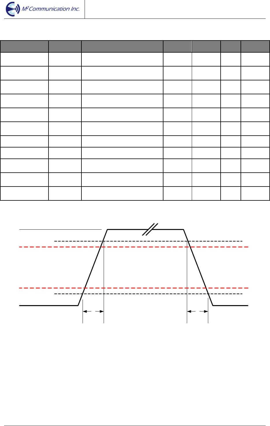
Table 4. Digital IO Specification
Parameter Symbol Condition Min Typ Max
Unit
Rise Time Tr 10% to 90% of VCC
CL=10pF, DR<1:0>=11 10 ns
Fall Time Tf 10% to 90% of VCC
CL=10pF, DR<1:0>=11 10 ns
Logic “H”
Input Level VIH VDD-0.6
V
Logic “L”
Input Level VIL 0.6 V
Input
Capacitance Cpin 1 pF
Input
Impedance Zpin,hiZ DC, Configured as hi-Z 10M Ω
Zpin,pl DC, Configured as pull-low 100K Ω
Zpin,ph DC, Configured as pull-high 100K Ω
Maximal Output
Current Idrive programmable 1 4 8 mA
Logic “H”
Output Level VOH VDD-0.5
V
Logic “L”
Output Level VOL 0.5 V
Digital IO Specification Annotation
0.9VDD
0.1VDD
T
r
T
f
VIH
VIL
VOH
VOL
Figure6. I/O level diagram
Datasheet v1.0
MA903A1
2014/01 Copyright © by M
2
Communication Inc. Page 9 of 22
2 Pin Out
All VDDs are rated from 2.4V to 3.6V.
Pin # Pin Name Description Type[1]
I/O/PWR
1 RFIO RF Signal 50 ohm IO RF
2~20, 22~26,
32, 40, 47, 49
GND Board ground G 0
21 VDD1 Module Power Input. 2.4V~3.6V
VDD1+VDD2+VDD3+VDD_RF 150mA Requirement
P PWR
27 VDD2 Module Power Input. 2.4V~3.6V
VDD1+VDD2+VDD3+VDD_RF 150mA Requirement
P PWR
28 UART_RXD UART_RXD, Baud Rate = 460.8kbps D/A IO
29 UART_TXD UART_TXD, Baud Rate = 460.8kbps D/A IO
30 IO2 GPIO D IO
31 IO1 GPIO D IO
33 JTAG_CLK ICE CLK (debugger) D I
34 JTAG_DAT ICE DATA IN (debugger) D IO
35 SYS_RESET External reset input, No need RC Delay [2] SYS SYS
36, 44~46 NC No Connection
37 DEBUG_IO2 Debug UART_TXD, No connection D O
38 DEBUG_IO1 Debug UART_RXD, No connection D I
39 RF_TEST_IO1 RF Test Pin Data_Out, No connection D O
41 RF_TEST_IO2 RF Test Pin CLK_Out, No connection D O
42 LED2 LED Index, Driver current 3mA D IO
43 LED1 LED Index, Driver current 3mA D IO
48 VDD3 Module Power Input. 2.4V~3.6V
VDD1+VDD2+VDD3+VDD_RF 150mA Requirement
P PWR
50 VDD_RF Module Power Input. 2.4V~3.6V
VDD1+VDD2+VDD3+VDD_RF 150mA Requirement
P PWR
[1] D=digital, A=analog, P=power, G=ground
[2] Set this pin low reset chip to initial state, with internal pull-up
[3] External interrupt input
Datasheet v1.0
MA903A1
2014/01 Copyright © by M
2
Communication Inc. Page 10 of 22
3 Memory
MA903A1 is equipped with embedded 128KB flash memory and 1MB SRAM. The specification is
listed as below.
Currently MA903A1 does not support the external memory due to performance compromises,
4 Serial Interfaces
MA903A1 support the common serial data interfaces, including GPIO, and UART. Their timing and
specifications are addressed at the following sections.
4.1 General-purpose I/O (GPIO)
The functions of GPIOs are summarized as below:
Push-Pull output
Open-Drain output
Input only with high impendence (100K ~ 300Kohms)
All inputs with Schmitt trigger
I/O pin configured as interrupt source with edge/level setting
Supports input 5V tolerance
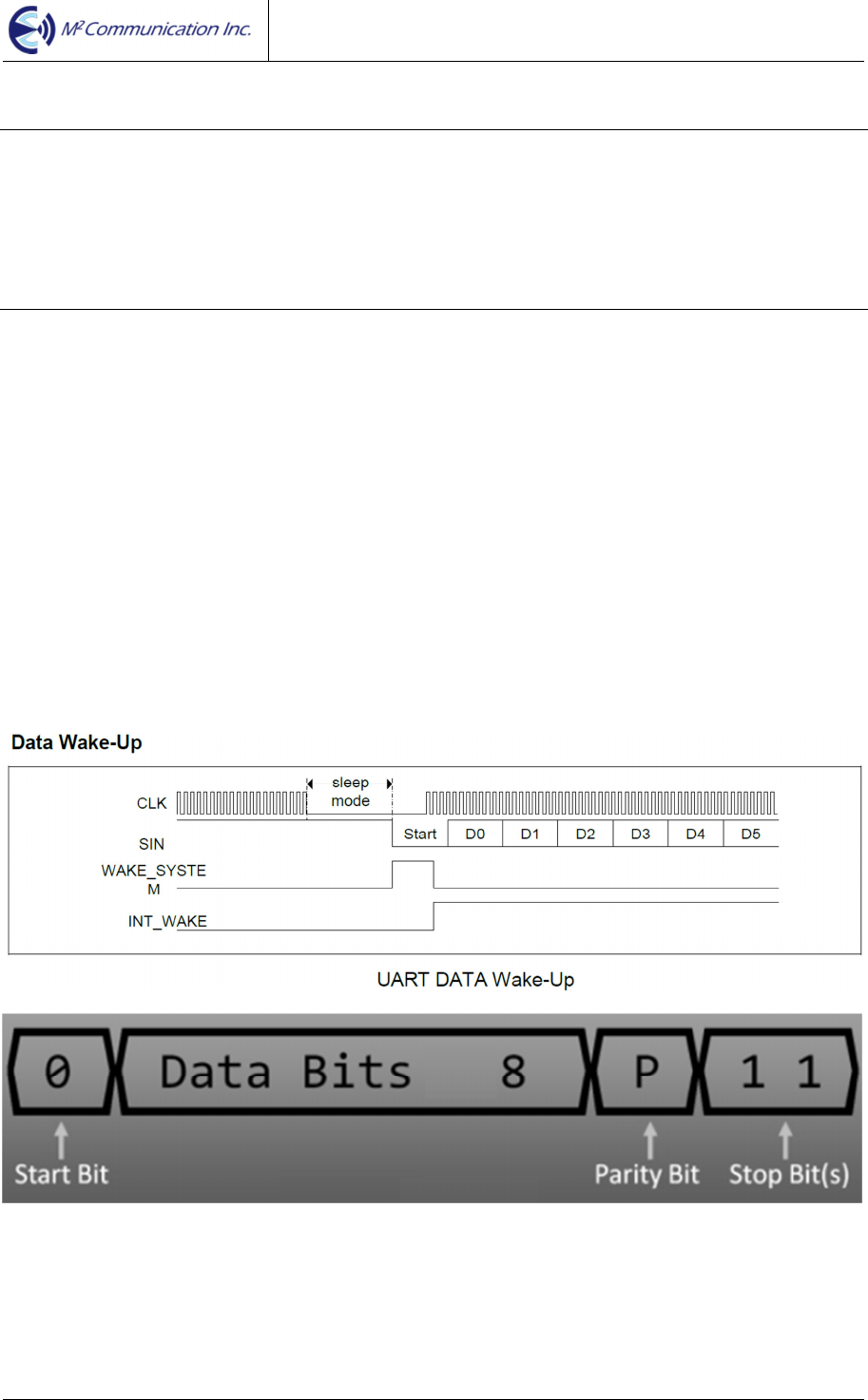
4.2 UART
Figure7. UART Data Format
The features of UART interfaces are summarized as below:
Two sets of UART controllers
The UART0 and UART1 are built-in with a 16-byte TX_FIFO and a 16-byte RX_FIFO to reduce
the number of interrupts presented to the CPU
Baud rate is up to 460800 bps
Datasheet v1.0
MA903A1
2014/01 Copyright © by M
2
Communication Inc. Page 11 of 22
5 How to Use MA903A1 to Design
The MA903A1 is a proprietary product design and manufactured by M2C (M
2
Communication Inc.) for
integrated into wireless products manufactured by M2C for sub 1GHz ISM communication application.
And the chapter will complete explain how to design MA903A1 on product.
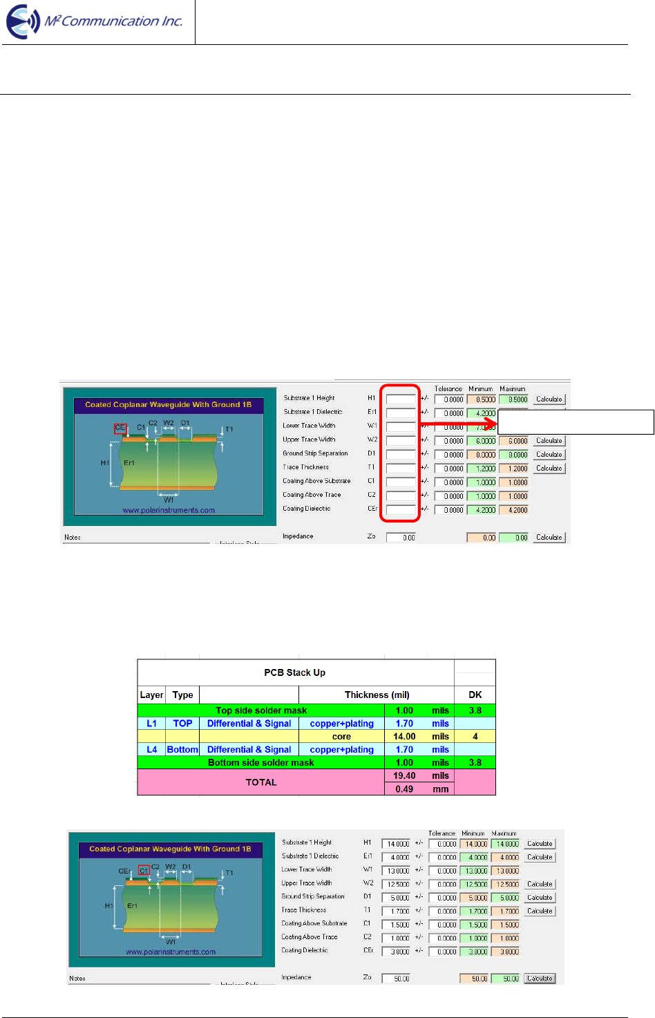
5.1 50ohm RF Trace Calculation
The MA903A1 module has 50ohm impedance RF output pin (RFIO) to connect external antenna on
carried board (or called Mother Board). RF trace on carried board is between RF output pin of
MA903A1 and antenna on carried board and the trace must is 50ohm to obtain best RF performance.
Also, 50ohm trace is recommended for PCB layout.
Engineer (or Developer) can use “PCB Transmission Line calculation tool” (example: Polar) to obtain
value about RF layout information on PCB. Engineer just fill in value that FR4relative parameter in
“PCB Transmission Line calculation tool”, include PCB stack, substrate height, PCB dielectric, trace
thickness….etc. 50ohm transmission line dimension can be got from the tool. Below figure10 show the
PCB Transmission Line calculation tool.
Figure8. Trace design for the PCB layout
Example: Use 2-layer FR4 PCB to design 50ohm trace
The figure 11 is 2-layers FR4 PCB parameter (PCB stack). The RF trace width and spacing that is
between RF trace and ground plane and others value that is 50ohm design requires is show in figure
12.
Figure9. 2-layer FR4 PCB stack
Figure10. 50ohm parameter of 2-layers FR4
Fill inFR4 Parameter
Datasheet v1.0
MA903A1
2014/01 Copyright © by M
2
Communication Inc. Page 12 of 22
5.2 PCB Design
MA903A1 provides 3 antennas (frequency: 902MHz~928MHz) for engineer chooses, one is PIFA type
antenna; the other two are dipole antenna. About antenna manufacturer and model number can refer
chapter 7.
When using dipole antenna on carried board, just need to make sure the impedance of RF trace is
50ohm, as below figure 11.
Figure11-1.Reversed SMA connector to connect dipole antenna
Figure11-2.Reversed SMA connector to connect dipole antenna
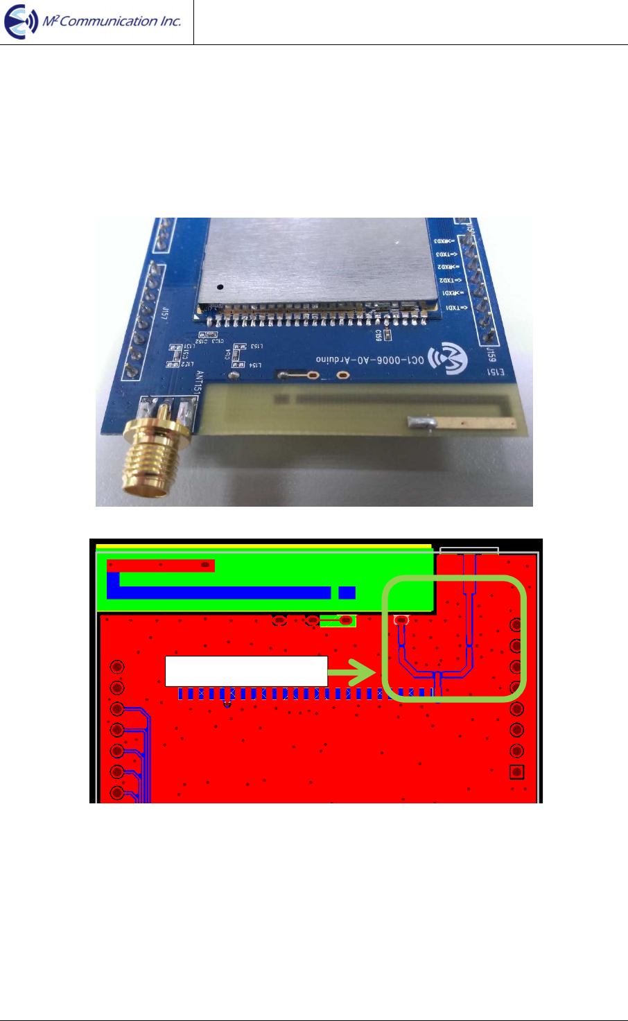
When using PIFA antenna in design PCB, need to make sure the impedance of RF trace is 50ohm.
Structure of PIFA antenna can separate two parts. One is metal part that solder on PCB; the other is
antenna trace on PCB. The different antenna trace length has different center frequency. Engineer
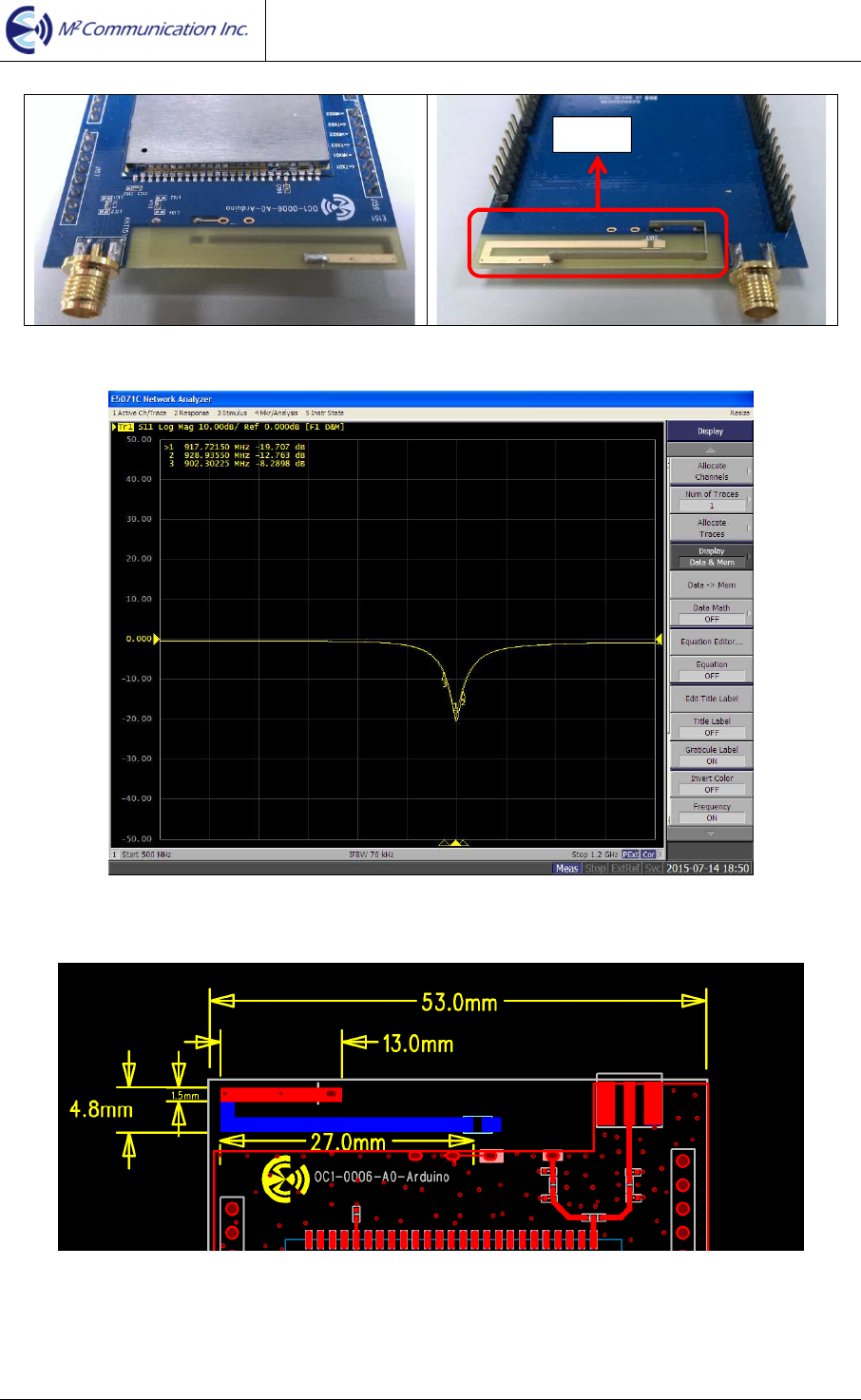
can use network analyzer to fine-tune antenna trace length, so that antenna can work on required
frequency (902MHz~928MHz). The trace dimension in figure14 is recommended to PCB layout.
50ohm RF
trace
Datasheet v1.0
MA903A1
2014/01 Copyright © by M
2
Communication Inc. Page 13 of 22
Figure12. PIFA antenna
Figure13. Network analyzer to check frequency & return loss
Figure14. PIFA antenna trace dimension
PIFA

Datasheet v1.0
MA903A1
2014/01 Copyright © by M
2
Communication Inc. Page 14 of 22
5.3 PCB Layout Recommend
RF connector: Reversed SMA connector.
RF trace length is less 80mm.
5.4 PCB Layout Guide
Some general rules of thumb for designing RF-related layouts for good RF performance are:
Use as much continuous ground plane metallization as possible.
Avoid the separation of the ground plane metallization at RF area.
Use as many grounding vias (especially near to the GND pins) as possible to minimize series
parasitic inductance between the ground pour and the GND pins.
Use a series of GND vias (a so called “via curtain”) along the PCB edges and internal GND metal
pouring edges. The maximum distance between the vias should be less than lambda/10 of the
10
th
harmonic. This is required to reduce the PCB radiation at higher harmonics caused by the
fringing field of these edges.
Avoid using long and/or thin transmission lines to connect the components. Otherwise, due to its
distributed parasitic inductance some detuning effects can occur.
Avoid using loops and long wires to obviate its resonances.
Always ensure good V
DD
filtering by using some bypass capacitors (especially at the range of
the operating frequency).
Datasheet v1.0
MA903A1
2014/01 Copyright © by M
2
Communication Inc. Page 15 of 22
6 Available Antenna List
The MA903A1 RF module has 50ohm RF output pin (RFIO) to connect external 902MHz~928MHz
antenna. The choice of antenna is limited to the antenna types the module has been tested with. Refer
to Section 8 “Regulation Approval” for a list of tested and approved antenna types that may be used
with the MA903A1 module.
A list of antenna approved for use with the module is provided as below table.
Antenna Type Peak Gain Model No. Manufacturer
PIFA 0.3dBi AN14-000079 RESILIENT
Dipole 1.42dBi CWX-614XSAXX-999
JOYMAX
Dipole 2dBi GWX-282XSABX-991
JOYMAX
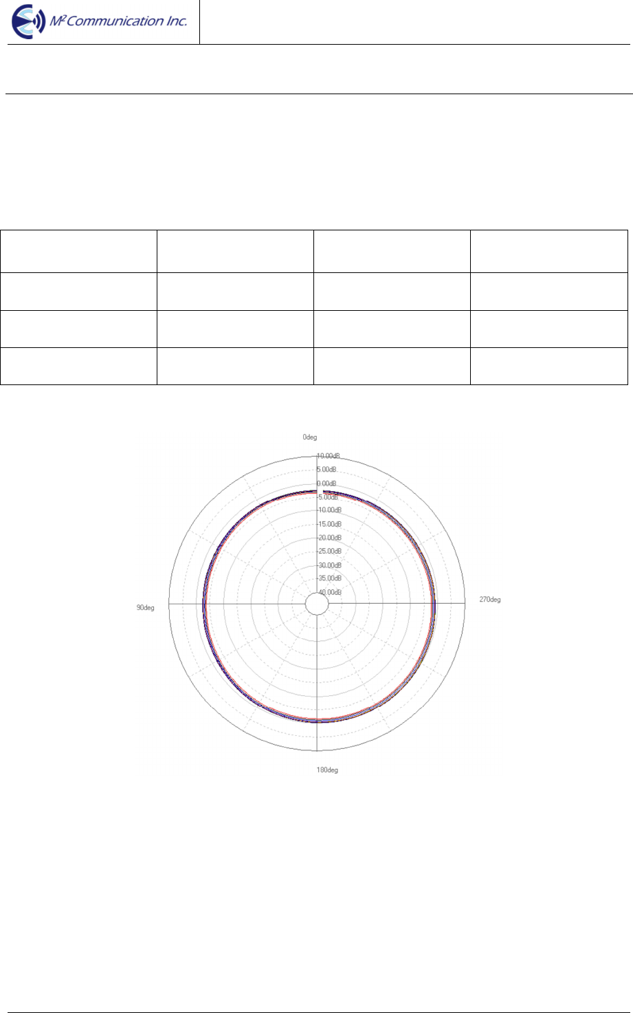
Below antenna’s pattern are measured and provide by vender.
PIFA / AN14-000079
X-Y Plane
Datasheet v1.0
MA903A1
2014/01 Copyright © by M
2
Communication Inc. Page 16 of 22
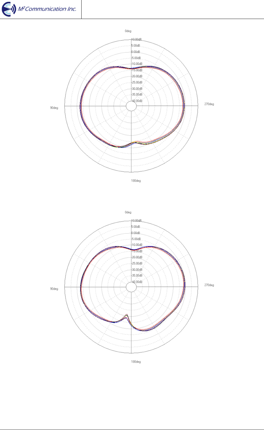
Y-Z Plane
X-Z Plane
Datasheet v1.0
MA903A1
2014/01 Copyright © by M
2
Communication Inc. Page 17 of 22
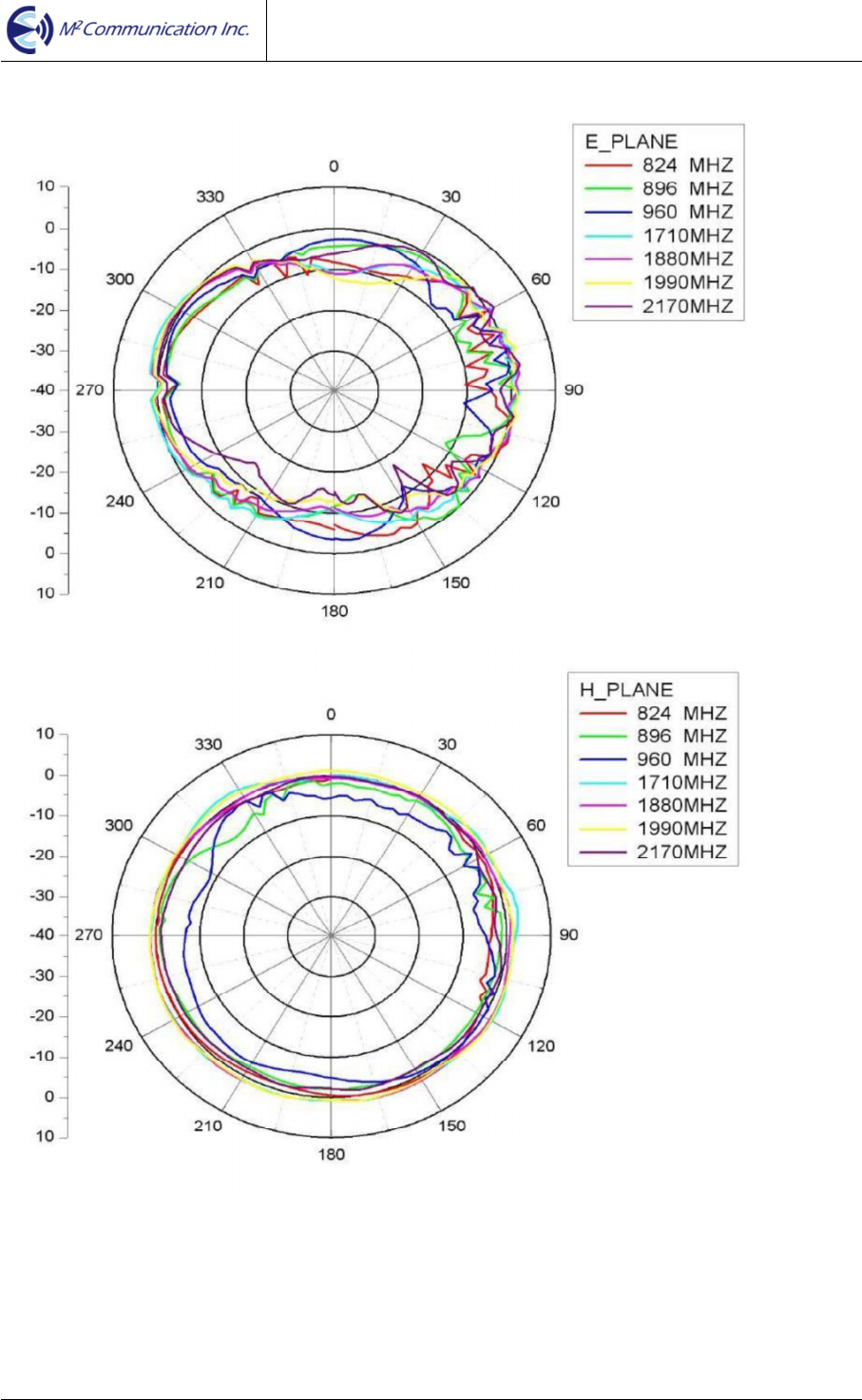
Dipole / CWX-614XSAXX-999
Datasheet v1.0
MA903A1
2014/01 Copyright © by M
2
Communication Inc. Page 18 of 22
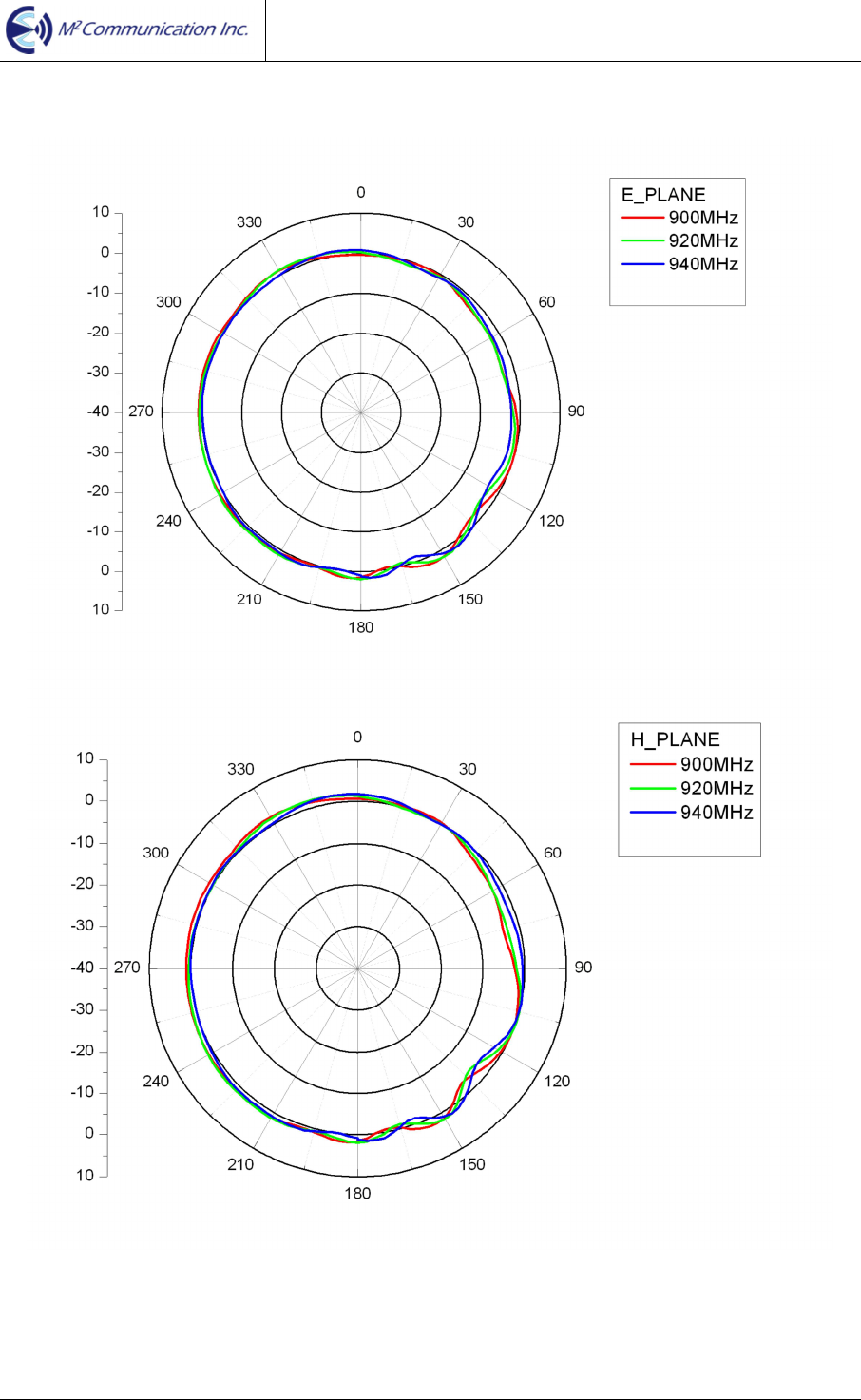
Dipole / GWX-282XSABX-991
Datasheet v1.0
MA903A1
2014/01 Copyright © by M
2
Communication Inc. Page 19 of 22
7 Regulation Approval
The MA903A1 module has received regulatory approvals for modular device in the United Stated.
Modular approval allows the end user to place the MA903A1 module inside a finish product and not
require regulatory testing for an intentional radiator (RF transmitter), provided no changes or
modifications are made to the module circuity. Changes or modifications could void the user’s
authority to operate the equipment. The end user must comply with all of the instructions provided by
the grantee, which indicate installation and/or operating conditions necessary for compliance.
The MA903A1 has received Federal Communications Commission (FCC) CFR47
Telecommunications, Part 15 Subpart C “Intentional Radiators” 15.247 and modular approval in
accordance with Part 15.212 modular Transmitter approval. The MA903A1 module can be integrated
into a finished product without obtaining subsequent and separate FCC approvals for intentional
radiation.
The MA903A1 module has been labeled with its own FCC ID number and if the FCC ID is not visible
when the module is installed inside another device, then the outside of the finished product into which
the module is installed must also display a label referring to the enclosed module. This exterior label
can use wording as follows:
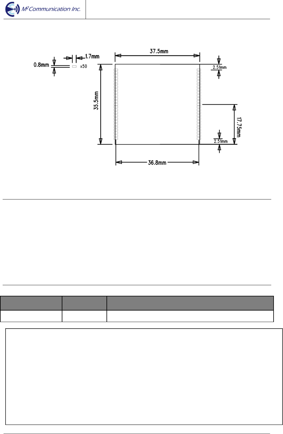
8 Recommended PCB Footprint
Figure15.Top View Outline Dimension
Contain Transmitter module FCC ID :
2AFXU
-
M
A
903A1
This device complies with Part 15 of the FCC Rules. Operation is subject to the following two
conditions:
(1) This device may not cause harmful interference, and (2) this device must accept any
interference received ,including interference that may cause undesired operation.
Datasheet v1.0
MA903A1
2014/01 Copyright © by M
2
Communication Inc. Page 20 of 22
Figure16.Recommend PCB Footprint
9 Contact Information
M
2
Communication Inc. (M2Comm)
4-3F, No.32, Gaotie 2nd Rd.,
Zhubei, Hsinchu County, Taiwan.
Tel: +886-3-657-8939
Fax: +886-3-657-6909
Email: sales@m2comm.com
www.m2comm-semi.com
10 Ordering Information
Ordering
Part Number
Frequency
Band
Product
Description
MA903A1 903~927MHz
MA903A1 with 50-ohm output for external antenna
This document contains confidential information and is subject to the terms and conditions set forth in the Non-
Disclosure Agreement between the Recipient Entity and M
2
Communication, Inc. (M2C) The information in this
document is believed to be accurate in all respects at the time of publication but is subject to change without
notice. M
2
Communication, Inc. assumes no responsibility for errors and omissions, and disclaims responsibility for
any consequences resulting from the use of information included herein. Additionally, M
2
Communication, Inc.
assumes no responsibility for the functioning of un-described features or parameters. M
2
Communication, Inc.
reserves the right to make changes without further notice. M
2
Communication, Inc. makes no warranty,
representation or guarantee regarding the suitability of its products for any particular purpose, nor does
M
2
Communication, Inc. assume any liability arising out of the application or use of any product or circuit, and
specifically disclaims any and all liability, including without limitation consequential or incidental damages.
M
2
Communication, Inc. products are not designed, intended, or authorized for use in applications intended to
support or sustain life, or for any other application in which the failure of the M
2
Communication, Inc. product could
create a situation where personal injury or death may occur. Should Buyer purchase or use M
2
Communication,
Inc. products for any such unintended or unauthorized application, Buyer shall indemnify and hold
M
2
Communication, Inc. harmless against all claims and damages.

Datasheet v1.0
MA903A1
2014/01 Copyright © by M
2
Communication Inc. Page 21 of 22
FCC Statement:
Federal Communication Commission Interference Statement
This equipment has been tested and found to comply with the limits for a Class B digital device,
pursuant to Part 15 of the FCC Rules. These limits are designed to provide reasonable protection
against harmful interference in a residential installation. This equipment generates, uses and can
radiate radio frequency energy and, if not installed and used in accordance with the instructions, may
cause harmful interference to radio communications. However, there is no guarantee that interference
will not occur in a particular installation. If this equipment does cause harmful interference to radio or
television reception, which can be determined by turning the equipment off and on, the user is
encouraged to try to correct the interference by one of the following measures:
●
Reorient or relocate the receiving antenna.
●
Increase the separation between the equipment and receiver.
●
Connect the equipment into an outlet on a circuit different from that to which the receiver is
connected.
●
Consult the dealer or an experienced radio/TV technician for help.
FCC Caution: Any changes or modifications not expressly approved by the party responsible
for compliance could void the user’s authority to operate this equipment.
This device complies with Part 15 of the FCC Rules. Operation is subject to the following two
conditions: (1) This device may not cause harmful interference, and (2) this device must accept any
interference received, including interference that may cause undesired operation.
This device and its antenna(s) must not be co-located with any other transmitters except in
accordance with FCC multi-transmitter product procedures.
Referring to the multi-transmitter policy, multiple-transmitter(s) and module(s) can be
operated simultaneously without C2P.
IMPORTANT NOTE:
FCC Radiation Exposure Statement:
This equipment complies with FCC radiation exposure limits set forth for an uncontrolled environment.
This equipment should be installed and operated with minimum distance 20 cm between the radiator &
your body.
IMPORTANT NOTE:
This module is intended for OEM integrator. The OEM integrator is responsible for
the compliance to all the rules that apply to the product into which this certified RF
module is integrated.
Additional testing and certification may be necessary when multiple modules are used.
20 cm minimum distance has to be able to be maintained between the antenna and the users for the
host this module is integrated into. Under such configuration, the FCC radiation exposure limits set
forth for an population/uncontrolled environment can be satisfied.
Any changes or modifications not expressly approved by the manufacturer could void the user's
authority to operate this equipment.
USERS MANUAL OF THE END PRODUCT:
In the users manual of the end product, the end user has to be informed to keep at least 20 cm
separation with the antenna while this end product is installed and operated. The end user has to be
informed that the FCC radio-frequency exposure guidelines for an uncontrolled environment can be
satisfied. The end user has to also be informed that any changes or modifications not expressly
approved by the manufacturer could void the user's authority to operate this equipment. If the size of
the end product is smaller than 8x10cm, then additional FCC part 15.19 statement is required to be
available in the users manual: This device complies with Part 15 of FCC rules. Operation is subject to

Datasheet v1.0
MA903A1
2014/01 Copyright © by M
2
Communication Inc. Page 22 of 22
the following two conditions: (1) this device may not cause harmful interference and (2) this device
must accept any interference received, including interference that may cause undesired operation.
LABEL OF THE END PRODUCT:
The final end product must be labeled in a visible area with the following " Contains TX FCC ID:
2AFXU-MA903A1 ". If the size of the end product is larger than 8x10cm, then the following FCC part
15.19 statement has to also be available on the label: This device complies with Part 15 of FCC rules.
Operation is subject to the following two conditions: (1) this device may not cause harmful interference
and (2) this device must accept any interference received, including interference that may cause
undesired operation.