MEIJIAXIN TOYS MD-01 2.4G module User Manual
Meijiaxin Toys Co., Ltd. 2.4G module
User manual
1、 Overview
MD-01 is a low-cost,low-power single-chip RF
transceiver module operatingin the 2.4GHz ISM
band. MD-01 is designed for a small amount
of data designed wireless controller.
2、Features
Frequency between the 2400MHz ~ 2483.5MHz;
Rate up to 250kbps, and high datathroughput;
Has high sensitivity (the rate at 10Kbps under-98dbm,
1% packet error rate)
Current consumption is very small, in the receive
mode current is15.6mA;
Design of the output power up to +1 dbm;
Built-in CRC error detection hardware circuits and
protocols
Support for asynchronous transparent receive
and transmit mode,and is compatible with existing
wireless communication protocol
3、Principles and external chip module block diagram
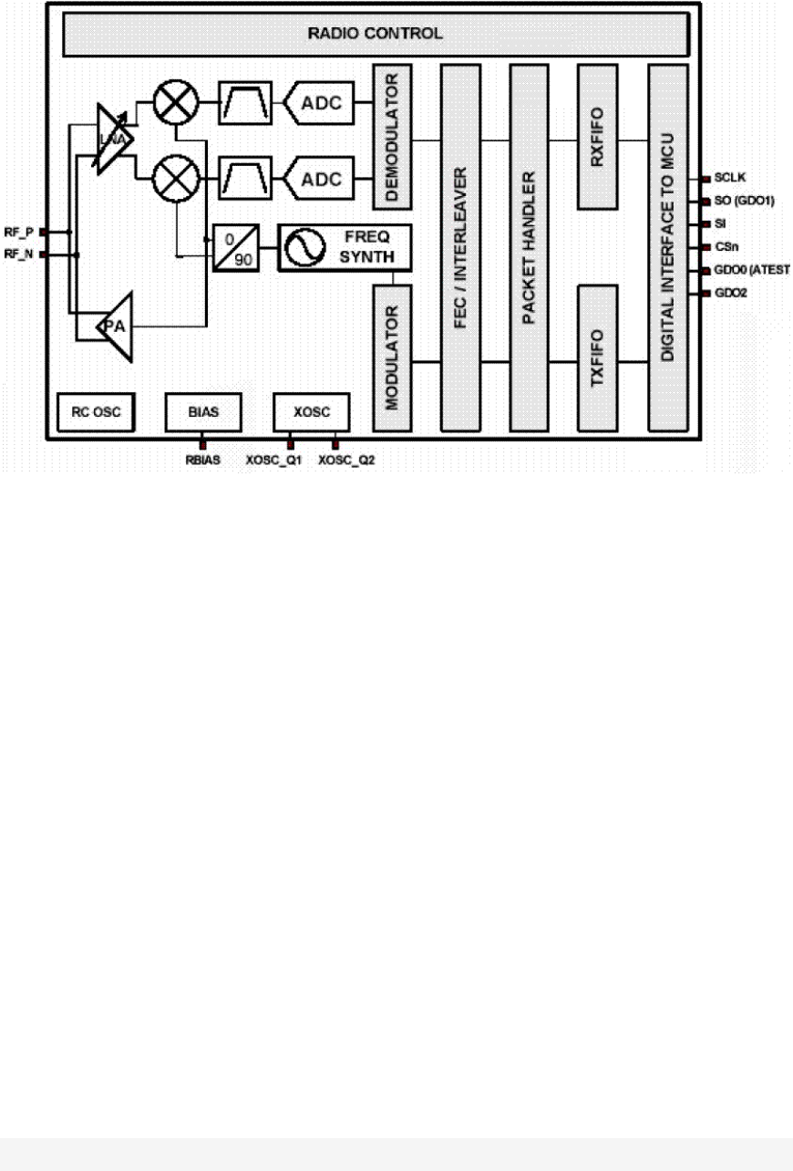
4、Description
1)RF receive mode
MD-01(MC-01) at VDD = 3.0V, Tc = 25 ° condition, the
receiversensitivity is -88dBm at the rate of 250Kbps ,
10kbps rate when-98dBm, the digital channel filter
bandwidth between the 58~650KHz bandwidth limit should
be crystal proportional to the frequency.
2)RF transmit mode
MD-01's output power between-30dBm ~ +1 dBm,
and spuriousradiation in the frequency of 25MHz ~ 1GHz ,is
-36dBm, at 47 ~ 74,87.5 ~ 118,174 ~ 230,470 ~ 862MHz is
-54dBm, the 1800MHz ~ 1900MHz (restricted band in
Europe) is as-47dBm, and in 2 * RF 3 * RF (U.S.
restrictions on the band) when -41dBm, the other is -30dBm
when the frequencies above 1GHz.
3)4-wire configuration interface
When the MD-01 in a subordinate position, it's SI, SO,

SCLK,CSn four port is configured as a simple
4-wire synchronous parallel ports, which are also used as
a buffer to read and writedata.
All the parallel port data transfer begins with the first byte,
includinga read/write signal, the pulse signal and
a 6-byte address.
During the address and data transmission,
CSn pin (chip select,active low) must be kept low. If
the transfer to take to CSn high, the transmission will be
terminated.
When CSn is set low, the microcontroller must wait for
theMD-01's low SO pin is set to begin after the
first byte transfer, indicating that the voltage regulator has
stabilized, crystal work,unless the transfer is
completed or the chip in sleep state, CSn pin is set low after
the SO pin will be set low.
4)Modulation
MD-01 supports amplitude modulation, frequency
shift keying and phase shift keying mode
a) Amplitude modulation
MD-01 supports two different forms of amplitude
modulationmode: off keying and amplitude shift keying. Off
keyingmodulation, respectively, through simply set to "1"
or "0" to turn onor turn off power make a big function,
and amplitude shift keyingcan be programmed to adjust to a
more sophisticated range ofsizes.
b) Frequency Shift Keying
FSK symbol coding as follows:
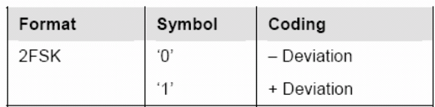
c) Phase shift keying
Phase shift keying is in transit to maintain a certain Period
to transmit data.
5)Wireless Control
a) Running order
When the power is turned on, the system mustbe reset.
In one of two ways must be executed: automatic restart or
manual restart
From time to time re-configuration is as follows:
SCLK set to "1" while SI is set to "0"
to avoid pin control modemay arise.
Strobe CSn set high
At least 40us CSn is high
CSn low and wait for SO to be set low, then there
is data to send or receive
The synchronous reset signal gating
When the SO once again set low,
the reset is complete and thechip is idle
b) Mode
MD-01 has two operating modes: receive and
send. These patterns through the micro-controller
SRX or STX strobecommands to directly activate,
or wake up automatically by thewireless.
c) Wireless wake-up (WOR) functionality
This optional wireless wake-up function can make
the MD-01periodically wake up from a deep sleep.
This function WOR has twocontrol modes choose to
rely on PKTCTRL1.AUTOSYNCbits. When this bit is
set to "0", the module will be wireless wake up in
the Event0 point in time, and enters the RX
State Event1point, which will ensure access
to RX state at the exact time.

5、Limit rating
Parameter Min Max Unit Remarks
Input voltage 1.8 3.6 V All power supply pin
have the same voltage
input
Max output
power
1 dbm
Max
data transfer
rate
250 Kbps
Operating
Temperature
-40 85 °C
Storage
Temperature
-50 150 °C
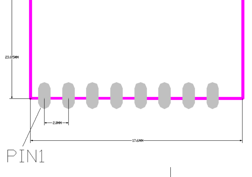
6、Module size and pin description
Module size
FCC Caution: Any changes or modifications not expressly
approved by the party responsible for compliance could void
the user's authority to operate this equipment.
This device complies with Part 15 of the FCC Rules.
Operation is subject to the following two conditions: (1) This
device may not cause harmful interference, and (2) this
device must accept any interference received, including
interference that may cause undesired operation.
This device and its antenna(s) must not be co-located or
operating in conjunction with any other antenna or
transmitter.
15.105 Information to the user.
(b) For a Class B digital device or peripheral, the instructions
furnished the user shall include the following or similar
statement, placed in a prominent location in the text of the
manual:
Note: This equipment has been tested and found to comply
with the limits for a Class B digital device, pursuant to part 15
of the FCC Rules. These limits are designed to provide
reasonable protection against harmful interference in a
residential installation. This equipment generates, uses and
can radiate radio frequency energy and, if not installed and
used in accordance with the instructions, may cause harmful
interference to radio communications. However, there is no
guarantee that interference will not occur in a particular
installation. If this equipment does cause harmful interference
to radio or television reception, which can be determined by
turning the equipment off and on, the user is encouraged to
try to correct the interference by one or more of the following
measures:
—Reorient or relocate the receiving antenna.
—Increase the separation between the equipment and
receiver.
—Connect the equipment into an outlet on a circuit different
from that to which the receiver is connected.
—Consult the dealer or an experienced radio/TV technician
for help.
Radiation Exposure Statement:
This equipment complies with FCC radiation exposure limits
set forth for an uncontrolled environment.
This transmitter must not be co-located or operating in
conjunction with any other antenna or transmitter.
The availability of some specific channels and/or operational
frequency bands are country dependent and are firmware
programmed at the factory to match the intended destination.
The firmware setting is not accessible by the end user.
.
The final end product must be labelled in a visible area with the following:“Contains
Transmitter Module FCC ID: TRIMD-01”

MD-01 pin description
Pin Name Pin Function Description
1 VCC Power supply Positive power supply
2 SI Digital input Configuration
mode input
3 SCLK Digital input Configuration mode, the
clock input
4 SO Digital input Configuration
mode output
5 GDO2 Digital input Configuration mode to
read data
6 GND Ground Ground
7 GDO0 Digital input / output As a general purpose
digital output
8 CSn Digital input Chip select
Configuration mode
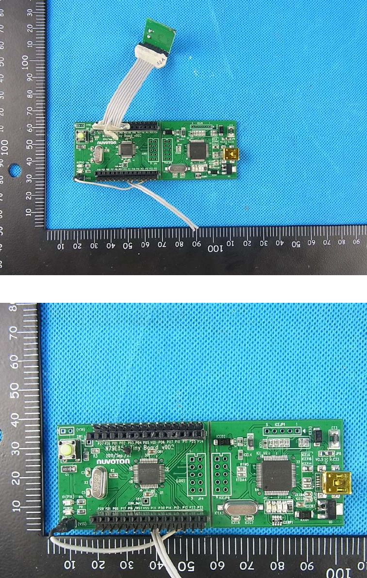
Control PCB + MD-01
Control PCB