MICROCHIP TECHNOLOGY BM78ABCDEFGH Bluetooth Module User Manual BM78 RN4678 datasheet 20150922 f
Microchip Technology Inc. Bluetooth Module BM78 RN4678 datasheet 20150922 f
Manual
Advanc
e
Information
2015 Microchip Technology Inc.
page
1
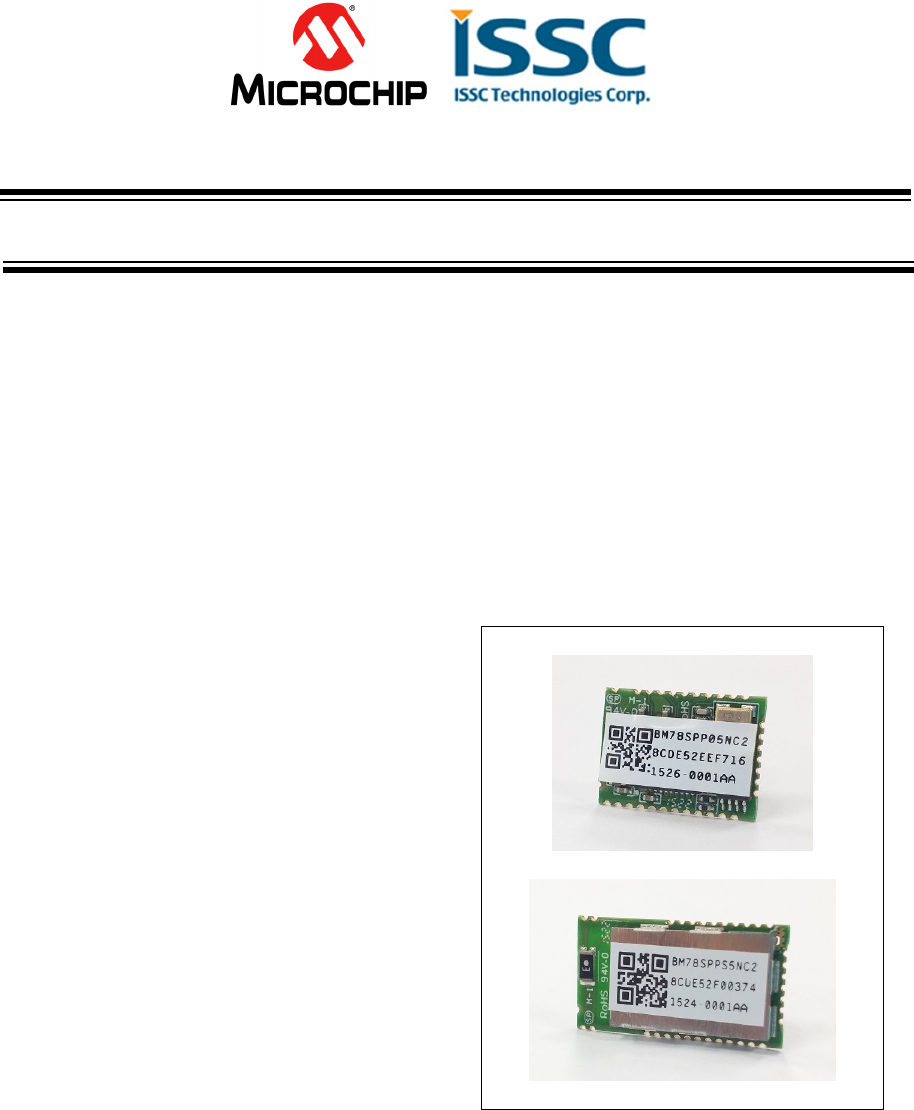
BM78SPPS5MC2,RN4678
Bluetooth
®
4.0 Dual mode Module
Features:
•
Bluetooth Classic (BR/EDR) and Low
Energy (LE)
•
Complete , Fully Certified, Embedded 2.4
GHz Bluetooth® Version 4.0 IC
•
Bluetooth SIG Certified
•
Transparent UART mode for seamless
serial data over UART interface
•
Easy to configure with Windows GUI or
direct by MCU
•
Firmware can be field upgradable via UART
•
Compact surface mount module: 22 x 12 x
2.4 mm
•
Castellated surface mount pads for easy
and reliable host PCB mounting
•
Perfect for Portable Battery Operated
Devices
•
Internal Battery Regulator Circuitry
•
Worldwide regulatory certifications
•
1 LED and it has 16 steps Brightness.
Operational:
•
Single operating voltage: 3.2V to 4.3V
•
Temperature range: -20℃ to 70℃
Industrial
•
Simple, UART interface
•
Integrated crystal, internal voltage
regulator, and matching circuitry
•
Multiple I/O pins for control and status
RF/Analog:
•
Frequency: 2.402 to 2.480 GHz
•
Receive Sensitivity: -90 dBm (BR/EDR); -92
dBm (LE)
•
Power Output: +2 dBm (typ.)
Data Throughput:
•
11k bps (BR/EDR)@ UART baud Rate is 115200
bps
•
8 Kbps (LE) UART baud Rate is 115200 bps
MAC/Baseband/Higher Layer:
•
Secure AES128 encryption
•
BTv3.0: GAP, SPP, SDP, RFCOMM and L2CAP
•
BTv4.0: GAP, GATT, ATT, SMP and L2CAP.
FIGURE 1: BM78 TOP VIEW
General Description:
The BM78 is a fully-certified Bluetooth®
Version 4.0 (BR/EDR/LE) IC for designers who
want to easily add dual mode Bluetooth®
wireless capability to their products.
Advanc
e
Information
2015 Microchip Technology Inc.
page
2
Delivering local connectivity for the
Internet of Things (IoT), the IC bridges your
product to Smart Phones and Tablets for
convenient data transfer, control and
access to cloud applications.
It supports GAP, SDP, SPP, and GATT
profiles. Data is transferred over the
Bluetooth link by sending/receiving data
via transparent UART mode, making it easy
to integrate with any processor or
Microcontroller with a UART interface.
Configuration is made easy using a
Windows® based GUI or directly via UART
by a MCU
Applications:
•
Mobile Point of Sales (mPOS)
•
LED lighting (16 step)
•
Wearables
•
Digital Sports
•
Fitness Devices
•
Health Care/ Medical
•
Automotive Accessories
•
Home Automation
•
Remote Control Toys

Advanc
e
Information
2015 Microchip Technology Inc.
page
3
BM78SPPS5M
C2
, RN4678
TO OUR VALUED CUSTOMERS
It is our intention to provide our valued customers with the best documentation possible to ensure successful use of your Microchip
products. To this end, we will continue to improve our publications to better suit your needs. Our publications will be refined and
enhanced as new volumes and updates are introduced.
If you have any questions or comments regarding this publication, please contact the Marketing Communications Department via
E-mail at docerrors@microchip.com. We welcome your feedback.
Most Current Data Sheet
To obtain the most up-to-date version of this data sheet, please register at our Worldwide Web site at:
http://www.microchip.com
You can determine the version of a data sheet by examining its literature number found on the bottom outside corner of any page.
The
last character of the literature number is the version number, (e.g., DS30000000A is version A of document DS30000000).
Errata
An errata sheet, describing minor operational differences from the data sheet and recommended workarounds, may exist for current
devices. As device/documentation issues become known to us, we will publish an errata sheet. The errata will specify the revision
of silicon and revision of document to which it applies.
To determine if an errata sheet exists for a particular device, please check with one of the following:
Microchip’s Worldwide Web site; http://www.microchip.com
Your local Microchip sales office (see last page)
When contacting a sales office, please specify which device, revision of silicon and data sheet (include literature number) you are
using.
Customer Notification System
Register on our web site at www.microchip.com to receive the most current information on all of our products.

Advanc
e
Information
2015 Microchip Technology Inc.
page
4
BM78SPPS5M
C2
, RN4678
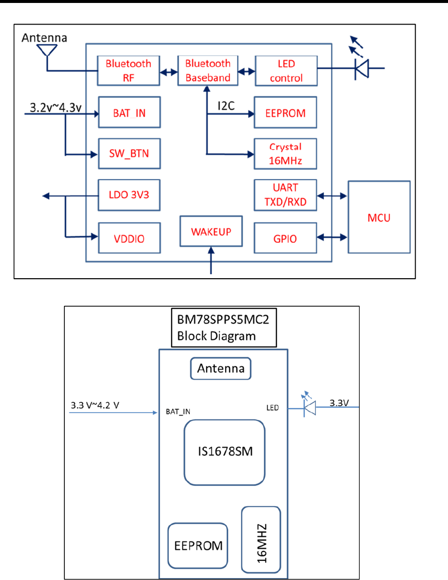
1.0 DEVICE OVERVIEW
The BM78 is a complete, fully certified, embedded 2.4 GHz Bluetooth® version 4.0
(BR/EDR/LE) wireless IC. It incorporates an on-board Bluetooth stack, cryptographic accelerator,
power management subsystem, 2.4 GHz transceiver, and RF power amplifier (see Figure 1). With
the BM78, designers can embed Bluetooth functionality rapidly into virtually any device.
The BM78 provides cost and time-to-market savings as a self-contained Bluetooth solution.
The IC has been designed to provide integrators with a simple Bluetooth solution that features:
• Ease of integration and programming
• Vastly reduced development time
• Minimum system cost
• Interoperability with Bluetooth hosts
• Maximum value in a range of applications
The BM78 can independently maintain a low-power wireless connection. Low-power usage
and flexible power management maximize the IC’s lifetime in battery-operated devices. A wide
operating temperature range allows use in indoor and outdoor environments (industrial
temperature range).
The BM78 module comes in two varieties. The BM78SPPS3MC2 is a complete, fully
regulatory certified
module with integral ceramic chip antenna and shield. The BM78SPP03MC2 is
a lower cost alternative
with external antenna and no shield. The integrator is responsible for the
antenna, antenna matching,
and regulatory certifications.
The BM78 is a small, compact, surface mount module with castellated pads for easy and
reliable host
PCB mounting. The module is compatible with standard pick-and-place equipment.
TABLE 1‐1: BM78 MODULE FAMILY TYPES
Device
Antenna
Shield
Regulatory
C
e
rtifications
BM7
8
SPPS
5N
C
2
Integral
cer
a
mi
c
ch
i
p
Yes
FCC,
IC,
CE,
KCC,
NCC,
Japan
BM7
8
SPP0
5N
C2
External
No
NO
FIGURE 1: Block Diagram
Advanc
e
Information
2015 Microchip Technology Inc.
page
5
BM78SPPS5M
C2
, RN4678
Advanc
e
Information
2015 Microchip Technology Inc.
page
6
BM78SPPS5M
C2
, RN4678
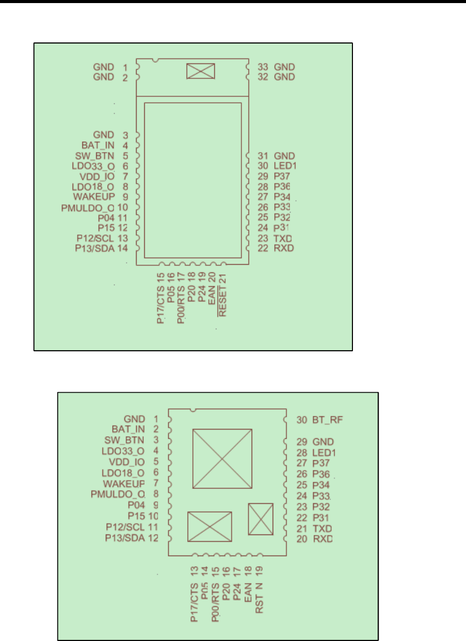
FIGURE 1‐2: BM78SPPS5NC2 PIN DIAGRAM
FIGURE 1‐3: BM78SPP05NC2 PIN DIAGRAM

Advanc
e
Information
2015 Microchip Technology Inc.
page
7
BM78SPPS5MC2 , RN4678
TABLE 1‐1: PIN DESCRIPTION
S5
pin
03
pin Symbol Type Description
1 -- GND Power Ground reference
2
--
GND
Power
Ground reference
3 1 GND Power Ground reference
4 2 BAT_IN Power Battery Input. Main positive supply input.
Connect to 10
uF
(X5R/X7R)
capacitor.
5 3 SW_BTN DI Software Button H: Power On / L: Power Off
6 4 LDO33_O Power Internal 3.3V LDO regulator output.
Connect to 10
uF
(X5R/X7R)
capacitor.
7 5 VDD_IO Power I/O positive supply input.
Ensure VDD_IO and MCU I/O voltages are compatible.
8 6 LDO18_O Power Internal 1.8V LDO regulator output.
Connect to 10uF (X5R/X7R) capacitor.
9 7 WAKEUP DI Wakeup from shutdown mode (active low)
(internal pull-up)
10 8 PMULDO_O Power Power management unit output.
Connect to 1
uF
(X5R/X7R)
capacitor.
11 9 P0_4 DO UART_TX_IND:
H: BM78 indicate UART data will be transmitted out
after certain timing.
(Setting by UI@ “MCU setting”, default wait 5ms)*1
L: Otherwise.
STATUS_IND_2:
BM78
State indication , refer to P1
_
5
12 10 P1_5 DO STATUS_IND:
B
luetooth link status indication
13
11
P1
_
2/SCL
DO
I2C SCL (Do Not Connect)
14
12
P1
_
3/SDA
DIO
I2C SDA (Do Not Connect)
15 13 P1_7/CTS DIO Configurable Control or Indication pin or
UART CTS (input)
16
14
P0
_
5
DIO
Configurable Control or Indication pin
17 15 P0_0/RTS DIO Configurable Control or Indication pin or
UART RTS (output)
18
16
P2
_
0
DI
System configuration (internal pull-up)
19 17 P2_4 DI System configuration (internal pull-up)
20
18
EAN
DI
System configuration (internal pull-down)
21 19 RST_N DI Module reset (active low) (internal pull-up)
Apply a pulse of at least 63 ns.
22
20
RXD
DI
UART data input
23
21
TXD
DO
UART data output
24 22 P3_1 DIO Configurable Control or Indication pin
(when configured as input: internal pull-up)
25 23 P3_2 DIO Configurable Control or Indication pin
(when configured as input: internal pull-up)
Advanc
e
Information
2015 Microchip Technology Inc.
page
8
BM78SPPS5MC2 , RN4678
26 24 P3_3 DIO Configurable Control or Indication pin
(when configured as input: internal pull-up)
27 25 P3_4 DIO Configurable Control or Indication pin
(when configured as input: internal pull-up)
28 26 P3_6 DIO (Do Not Connect)
29 27 P3_7 DIO Configurable Control or Indication pin
(when configured as input: internal pull-up)
30 28 LED1 DO Status LED
31
29
GND
Power
Ground reference
--
30
BT_RF
AIO
External antenna
connection (50 ohm)
32 -- GND Power Ground reference
33
--
GND
Power
Ground reference
Note 1: Pin type abbreviation: A = Analog, D = Digital, I = Input, O = Output.
UI setting:
Advanc
e
Information
2015 Microchip Technology Inc.
page
9
BM78SPPS5MC2 , RN4678
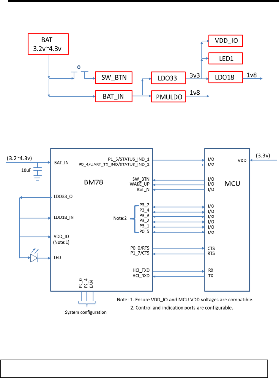
1.1 Power Tree
Figures 2-1 : Power Tree
1.2
UART Interface
Figures 2-2 : Power and MCU interface examples.
Figure 2‐2 shows an example power scheme using a 3.3 volt to MCU VDD. Battery power is
applied to BAT_IN pin. From the LDO33_O pin, voltage can be routed the VDD_IO pin and external
circuitry including the MCU. This power scheme ensures that BM78 and MCU I/O voltages are
compatible.
CAUTION: The internal 3.3volt LDO current source: 50mA maximum!!
Advanc
e
Information
2015 Microchip Technology Inc.
page
10
BM78SPPS5MC2 , RN4678
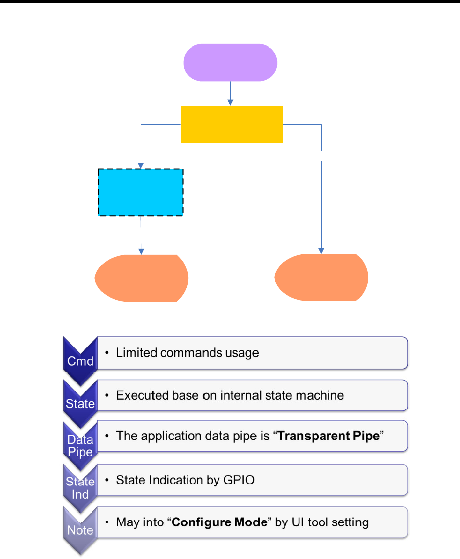
2.0 Bluetooth behavior auto/manual pattern configuration
2.1 auto pattern
Power ON
Auto Pattern Setting
Auto Pattern Manual Pattern
Configure Mode
Enabled
Disabled
Advanc
e
Information
2015 Microchip Technology Inc.
page
11
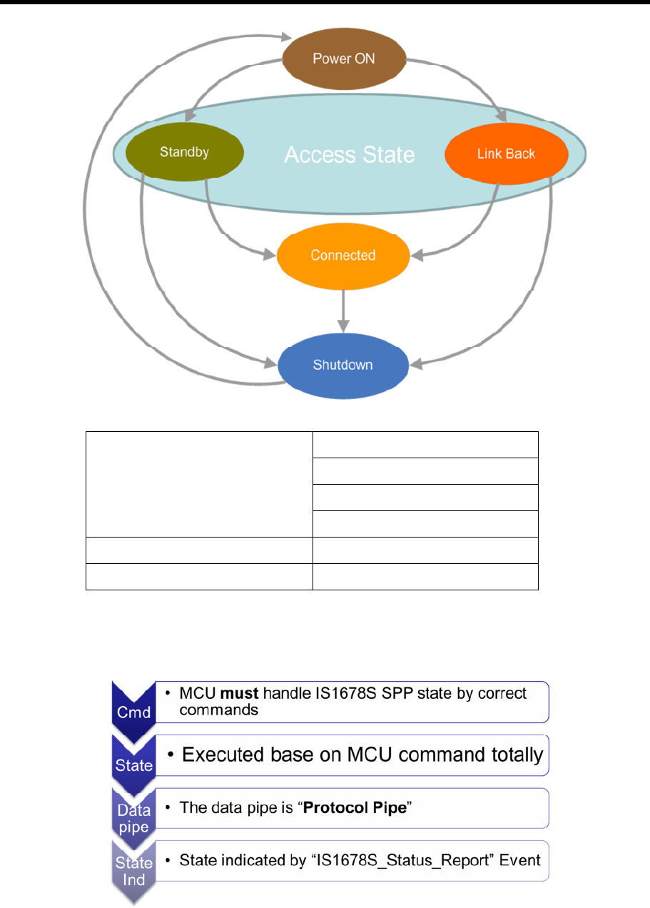
BM78SPPS5MC2 , RN4678
Access State
Configure mode
Standby mode
Link back mode
Pairing Procedure
Link state Connected mode
Shutdown state Shutdown mode
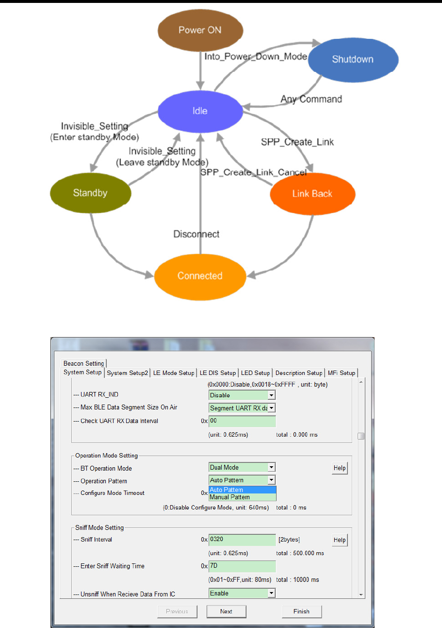
2.2 Manual pattern
Advanc
e
Information
2015 Microchip Technology Inc.
page
12
BM78SPPS5MC2 , RN4678
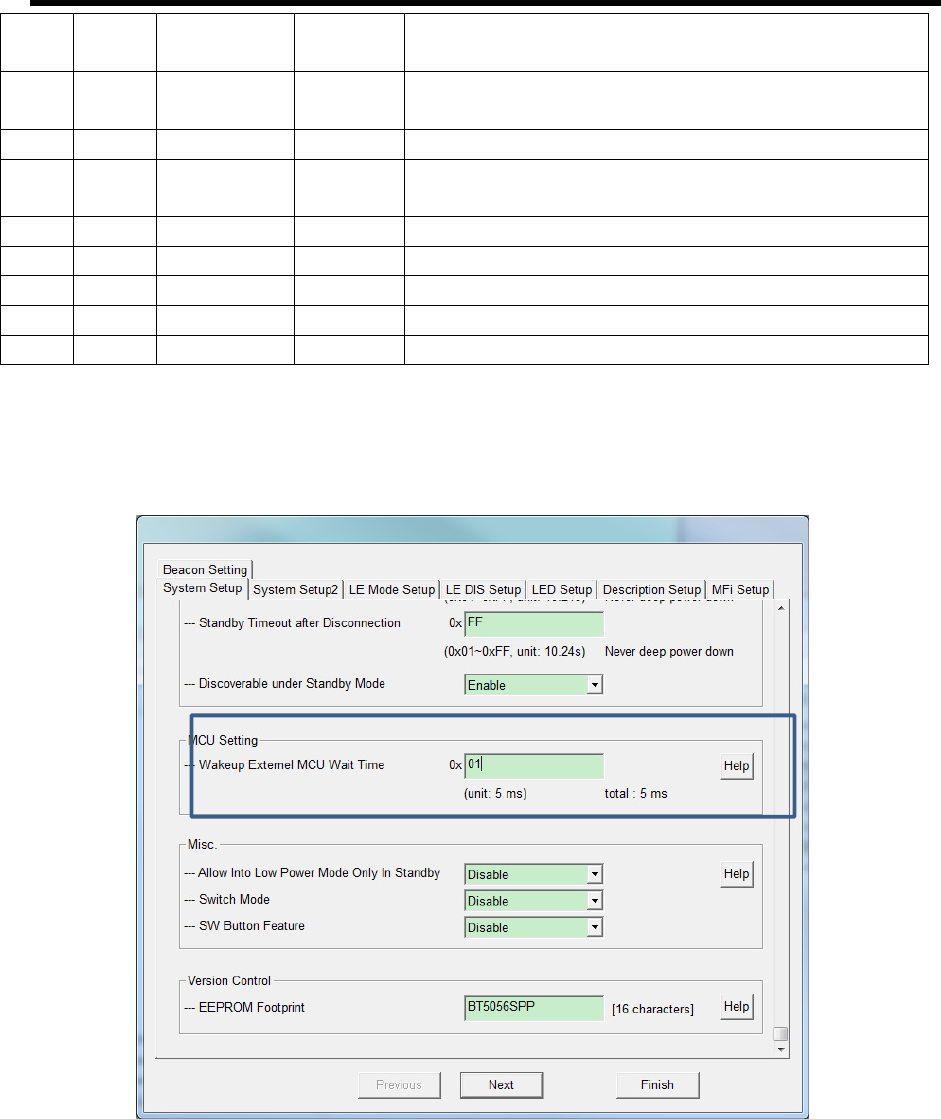
2.3 UI setting
NOTE: Please reference
“Application Note_IS1678S_Draft.docx”
and “IS1678S Command Set v0
97 20140924.docx.”
Advanc
e
Information
2015 Microchip Technology Inc.
page
13
BM78SPPS5MC2 , RN4678
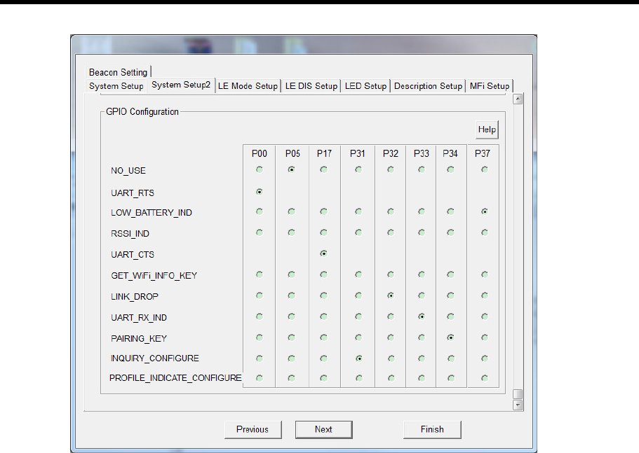
3.0
Control and Indication I/O Pins
I/O pins P0_0, P0_5, P1_7, P3_1, P3_2, P3_3, P3_4 and P3_7 are configurable control and
indication I/O. Control signals are input to the BM78. Indication signals are output from the BM78.
Table 4‐1 shows configurable I/O pin assignment to control and indication signals.
Note: that RTS can only be assigned to P0_0 and CTS is assigned to P1_7.
Configuring the BM78 can reference the “Application Note_IS1678S_Draft.docx” and
“IS1678S Command Set v0 97 20140924.docx.”
TABLE 3‐1: CONFIGURATION AND INDICATION I/O ASSIGNMENTS
N/C
UART_RTS
UART_CTS
LOW_BATTERY_IND
RSSI_IND
GET WIFI INFO KEY
LINK_DROP_CONTROL
(DISCONNECT)
UART_RX_IND
PAIRING_KEY
INQUIRY CONTROL
PROFILE_IND
P0_0
■
P0_5
■
P1_7
■
P3_1
■
P3_2
■
P3_3
■
P3_4
■
P3_7
■
Advanc
e
Information
2015 Microchip Technology Inc.
page
14
BM78SPPS5MC2 , RN4678
3.1 UI setting
Advanc
e
Information
2015 Microchip Technology Inc.
page
15
BM78SPPS5MC2 , RN4678
4.0
Status Indication I/O Pins
I/O pins P1_5 and P0_4 are Status Indicator 1 and 2 signals respectively. Together they
provide status indication to the MCU as shown in Table 4‐1.
TABLE 4‐1: STATUS INDICATION
P1_5
/STATUS_IND_1
P0_4
/STATUS_IND_2
Indication
H H Power-on to setting default and Shutdown State.
HH status should be stable for at least 500ms
H L Access state
L H Link state
(
UART data be
tween
being and stop
transmitted)
L L Link state (UART data stop transmitted)
4.1 System Configuration
I/O pins P2_0, P2_4, and EAN place the BM78 into operation modes as shown in Table 4‐2.
P2_0 , P2_4and EAN each have internal pull-ups.
TABLE 4‐2: SYSTEM CONFIGURATION SETTINGS
IC P2_0 P2_4 EAN Operational Mode
IS1678S Low High High Write EEPROM and test mode
High High High Normal operation / APP Mode
Advanc
e
Information
2015 Microchip Technology Inc.
page
16
BM78SPPS5MC2 , RN4678
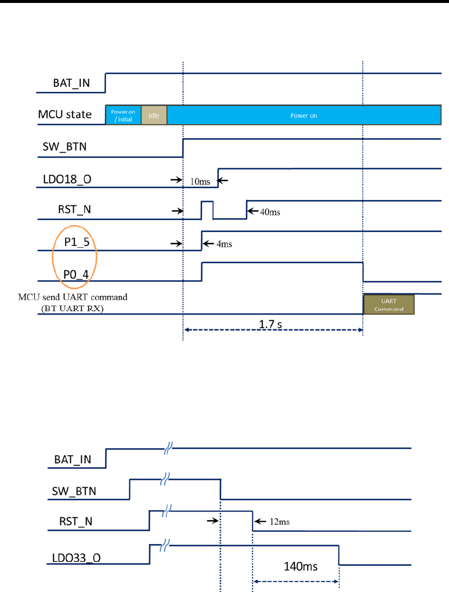
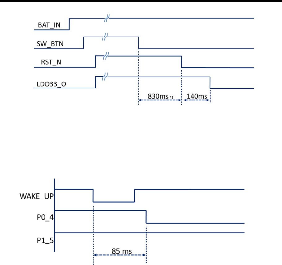
5.0 Software Button (SW_BTN)
The Software Button (SW_BTN) input pin powers the BM78 on (high) or off (low) in to S4 mode.
Figures 5‐1 : SW_BTN Time (high) @APP mode
Note:
A. P0_4/P1_5 state: Refer to table5-1
B. Reset is floating.
Figures 5‐2 : SW_BTN Time (low) at access states.
Note:
A. SW_BTN pull low can’t active on Shutdown State.
B. Reset is floating.
Figures 5‐3 : SW_BTN Time (low) at link states.
Advanc
e
Information
2015 Microchip Technology Inc.
page
17
BM78SPPS5MC2 , RN4678
Note:
C. *1: this time by iPhone LE mode disconnect time.
D. SW_BTN pull low can’t active on Shutdown State.
E. Reset is floating.
6.0 WAKE UP
The Wake Up input pin wakes the BM78 from shutdown mode (active low).
Figures 6‐1 : WAKE_UP Time at Shutdown State.
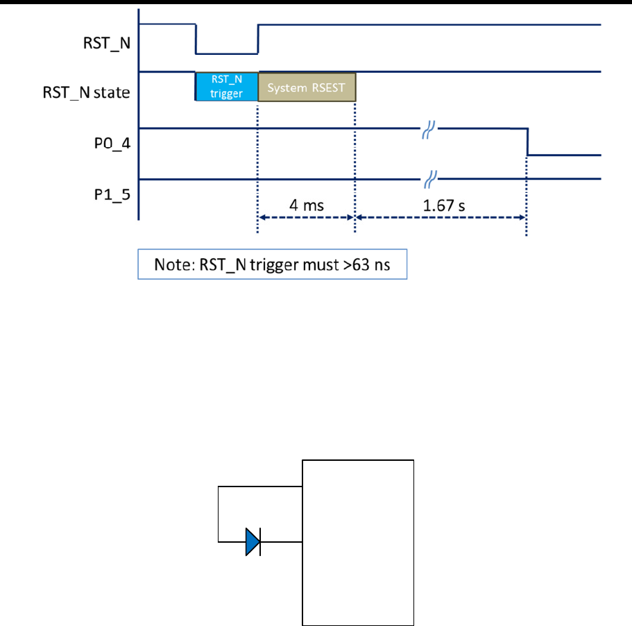
7.0 EXTERNAL RESET
A watchdog timer capable of reset the chip. It has an integrated Power-On Reset (POR)
circuit that resets all circuits to a known power-on state. This action can also be driven by an
external reset signal that can be used to externally control the device, forcing it into a power-on
reset state. The RST signal input is active low and no connection is required in most applications.
Figures 7 ‐1 : Reset Time at Shutdown State.
Advanc
e
Information
2015 Microchip Technology Inc.
page
18
BM78SPPS5MC2 , RN4678
Note:
a. Auto pattern can use external reset.
b. Manual pattern can use external reset and reset command.
8.0 LED DRIVER
There are one dedicate LED drivers to control the LEDs. The LED can be connected directly
with BM78. The LED max current is 4 mA and it has 16 steps to trim Brightness.
BM78
LED1
LDO33_O
The status LED (LED1) indicates:
Standby
Link Back
Low Battery
Inquiry
Link
Page
Each indication is a configurable flashing sequence. LED brightness can also be configured.
9.0 MEMORY
A synchronous single port RAM interface is used. There are sufficient ROM and RAM to
fulfill the requirement of processor. A register bank, a dedicated single port memory and a flash
memory are connected to the processor bus. The processor coordinates all the link control
procedures and data movement using a set of pointers registers.

Advanc
e
Information
2015 Microchip Technology Inc.
page
19
BM78SPPS5MC2 , RN4678
Advanc
e
Information
2015 Microchip Technology Inc.
page
20
BM78SPPS5MC2 , RN4678
10.0 Throughput
The BM78 UART pins TXD and RXD connect to the UART pins of the host MCU. It is highly
recommended to use hardware flow control pins RTS and CTS. The BM78 hardware flow control is
disabled by default and must be configured to enable. The UART Baud is configurable. The
available signal rates are listed in Table 10‐1.
TABLE 10‐1: UART BAUD
Baud Crystal Frequency (MHz) Actual Baud Error Rate (%)
921600 16 941176 2.12
460800 16 457143 -0.79
307200 16 307692 0.16
230400 16 231884 0.64
115200 16 117647 2.1
57600 16 57145 -0.97
38400 16 38462 0.16
28800 16 28623 -0.62
19200 16 19231 0.16
14400 16 14480 0.55
9600 16 9615 0.16
4800 16 4808 0.16
2400 16 2399 -0.03
TABLE 10‐2: APP mode Throughput report
BR/EDR mode iPad mini (Wi‐Fi disable){iOS 7.0.4 (11B554a)}
921600 bps echo Tx echo Rx Tx Rx
Burst Throughput(byte/s)
14384.46
9845.31 14521.5
14333.3
Normal
Throughput(byte/s) 8437.462
8375.28 6674.11
14399.4
BR/EDR mode iPad mini (Wi‐Fi disable){iOS 7.0.4 (11B554a)}
115200 bps echo Tx echo Rx Tx Rx
Burst Throughput(byte/s)
11080.55
9284.37 11640.3
11134.8
Normal
Throughput(byte/s) 6248.758
6211.69 11513 11158.4
BR/EDR mode Android Samsung Note3/Android 4.3
921600 bps echo Tx echo Rx Tx Rx
Normal
Throughput(byte/s) 9727.704
9041.34 17030.1
10233.6
Advanc
e
Information
2015 Microchip Technology Inc.
page
21
BM78SPPS5MC2 , RN4678
BR/EDR mode Android Samsung Note3/Android 4.3
115200 bps echo Tx echo Rx Tx Rx
Normal
Throughput(byte/s) 11312.2 10548.5 9842.5 11436.4
LE mode iPad mini (Wi‐Fi disable){iOS 7.0.4 (11B554a)}
115200 bps TX RX
(response)
Rx
(Reliable Burst Transmit)
Normal
Throughput(byte/s) 7935.2 3337.3 7082.1
LE mode iPad mini (Wi‐Fi disable){iOS 7.0.4 (11B554a)}
921600 bps TX RX
(response)
Rx
(Reliable Burst Transmit)
Normal
Throughput(byte/s) 8063.2 3384.5 6839.9

Advanc
e
Information
2015 Microchip Technology Inc.
page
22
BM78SPPS5MC2 , RN4678
11.0 Mounting Details
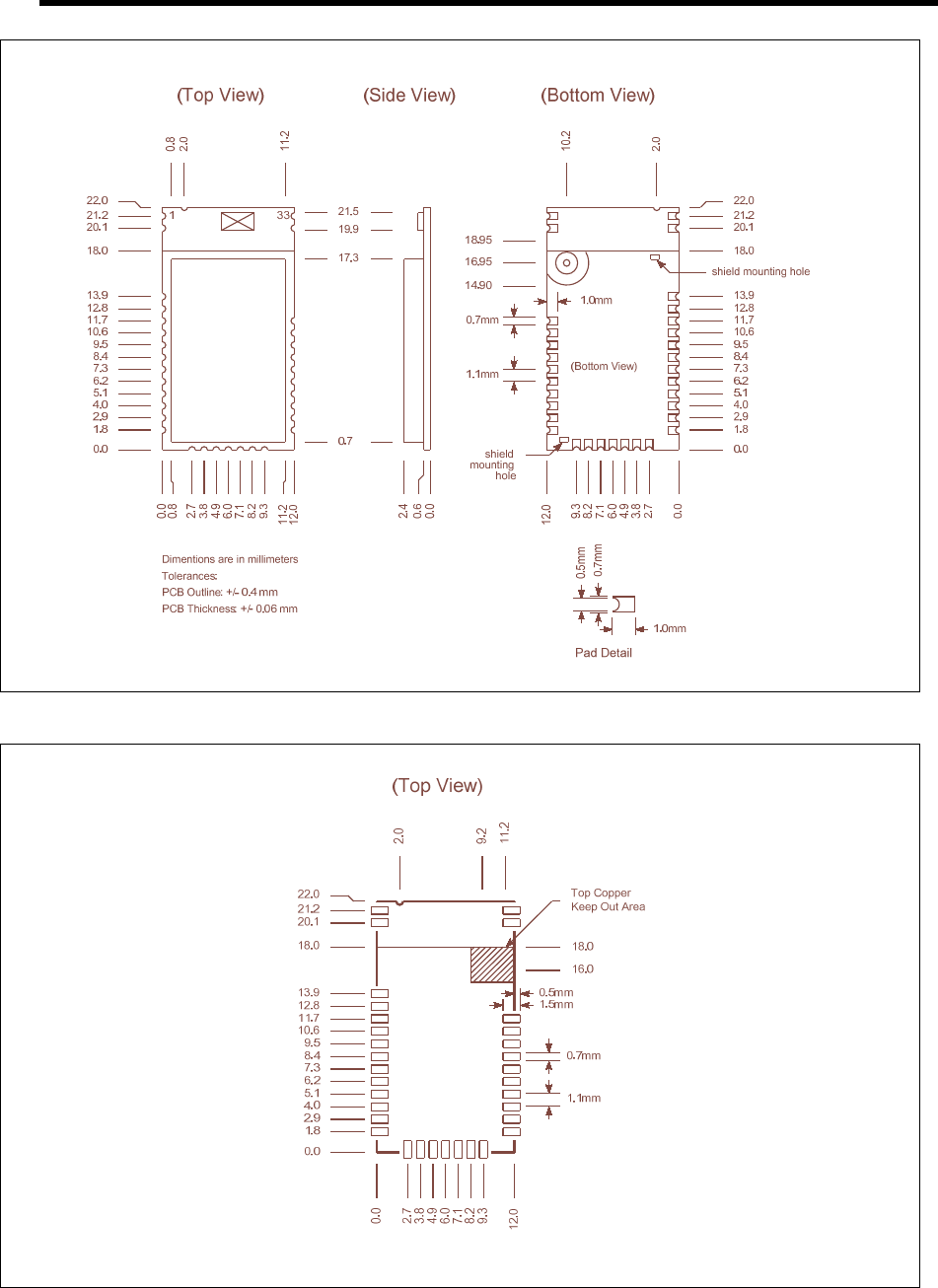
The BM78 SPPS5NC2 physical dimensions are shown in Figure 11-1, recommended host PCB footprint
in
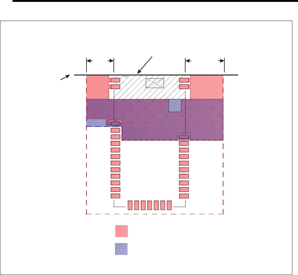
Figure 11-2, and mounting suggestion in Figure 11-3. There should not be top copper layer near the
test
pin area shown in Figure 11-2. When laying out the host PCB, the areas under the antenna should
not
contain any top, inner layer, or bottom copper as shown in Figure 11-3. A low-impedance ground
plane
will ensure best radio performance (best range, lowest noise). Figure 11-3 shows a minimum
ground
plane area to the left and right of the module for best antenna performance. The ground plane
can be
extended beyond the minimum recommended as need for host PCB EMC noise reduction. For
best
range performance, keep all external metal away from the ceramic chip antenna at least 31 mm.
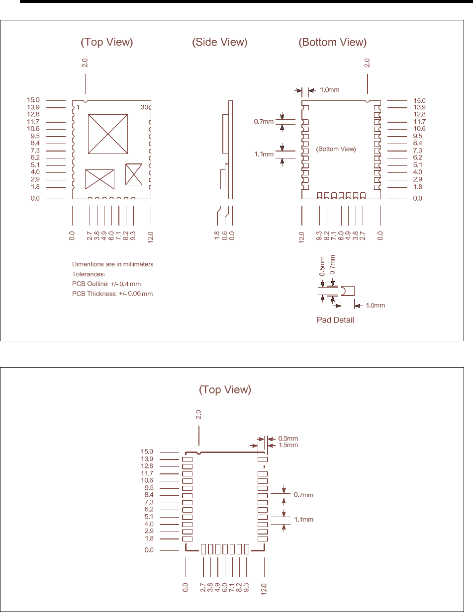
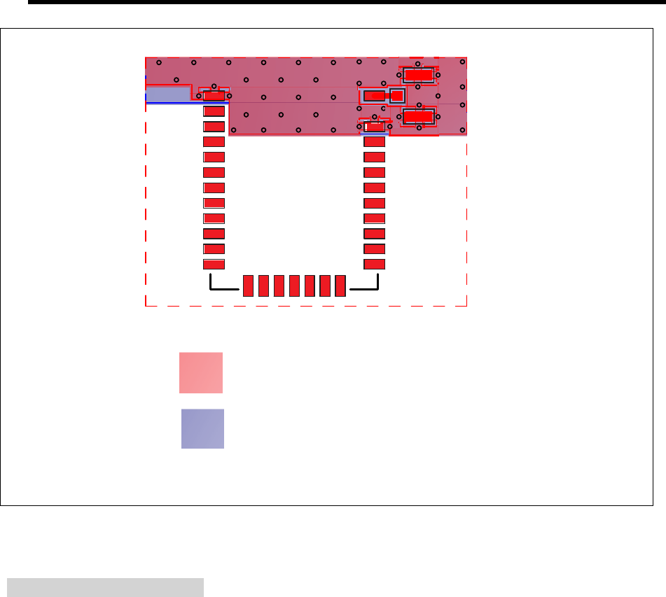
The BM78SPP03MC2 physical dimensions are shown in Figure 11-4, recommended host PCB footprint in
Figure 11-5, and mounting suggestion in Figure 11-6. It is highly recommended to layout the host PCB as
suggested in Figure 11-6. A low-impedance ground plane will ensure best radio performance (best
range, lowest noise). Pin 30 (BT_RF) is a 50 ohm connection to an external antenna connector, PCB
trace antenna, or component (ceramic chip) antenna through a host PCB 50 ohm micro-strip trace. This
trace can be extended to include passive parts for antenna attenuation padding, impedance matching,
or to provide test posts. It is recommended that the micro-strip trace be as short as possible for
minimum loss and best impedance matching. If the micro-strip trace is longer, it should be a 50 ohm
impedance. Figure 11-6 shows an example connection to U.FL connector.
Soldering Recommendations
The BM78 wireless module was assembled using standard lead-free reflow profile IPC/JEDEC J-STD-020.
The module can be soldered to the host PCB using standard leaded and lead-free solder reflow profiles.
To avoid damaging the module, the following recommendations are given:
•
Microchip Technology Application Note AN233 Solder Reflow Recommendation (DS00233)
provides solder reflow recommendations
•
Do not exceed peak temperature (T
P
) of 250 deg C
•
Refer to the solder paste data sheet for specific reflow profile recommendations
•
Use no-clean flux solder paste
•
Do not wash as moisture can be trapped under the shield
•
Use only one flow. If the PCB requires multiple flows, apply the module on the final flow.
Advanc
e
Information
2015 Microchip Technology Inc.
page
23
BM78SPPS5MC2 , RN4678
FIGURE 11‐1: BM78SPPS5NCS MODULE DIMENSIONS
FIGURE 11‐2: BM78SPPS5NC2 RECOMMEDED PCB FOOTPRINT
Advanc
e
Information
2015 Microchip Technology Inc.
page
24
BM78SPPS5MC2 , RN4678
FIGURE 11‐3: BM78SPPS5NCS HOST PCB MOUNTING SUGGESTION
Top and Bottom Copper
layer keep out area
Top Copper Layer
Bottom Copper Layer
>6.4mm
>4.7mm
Edge of
host PCB
Advanc
e
Information
2015 Microchip Technology Inc.
page
25
BM78SPPS5MC2 , RN4678
FIGURE 11‐4: BM78SPP05NCS MODULE DIMENSIONS
FIGURE 11‐5: BM78SPP05NC2 RECOMMEDED PCB FOOTPRINT
Advanc
e
Information
2015 Microchip Technology Inc.
page
26
BM78SPPS5MC2 , RN4678
FIGURE 11‐6: BM78SPP05NCS HOST PCB MOUNTING SUGGESTION
Top Copper Layer
Bottom Copper Layer
Advanc
e
Information
2015 Microchip Technology Inc.
page
27
BM78SPPS5MC2 , RN4678
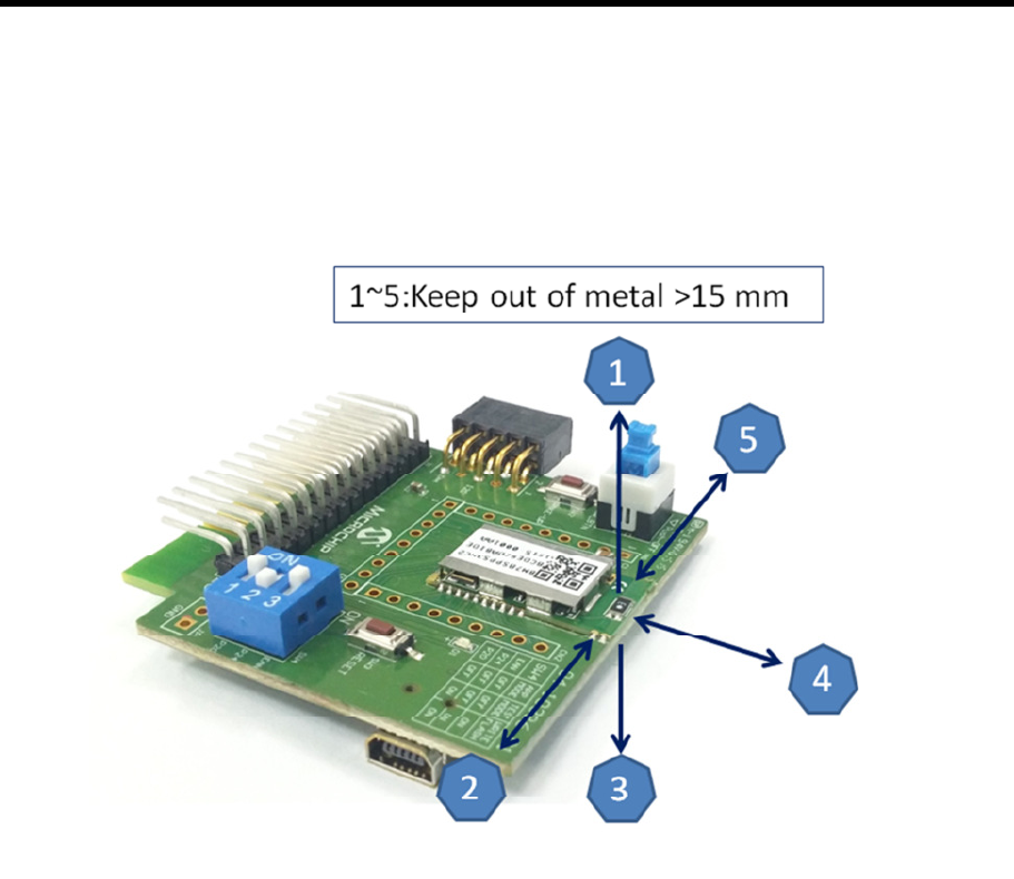
12.0 ANTENNA PLACEMENT RULE
For Bluetooth product, antenna placement will affect whole system performance.
Antenna need free space to transmit RF signal, it can’t be surround by GND plane.
Here are some examples of good and poor placement on a Main Application board with GND plane.
FIGURE 12-1: KEEP OUT AREA SUGGESTION FOR ANTENNA
For more detail free space of antenna placement design, you can reference the design rule of
antenna produce vendor.
Advanc
e
Information
2015 Microchip Technology Inc.
page
28
BM78SPPS5MC2 , RN4678
12-2
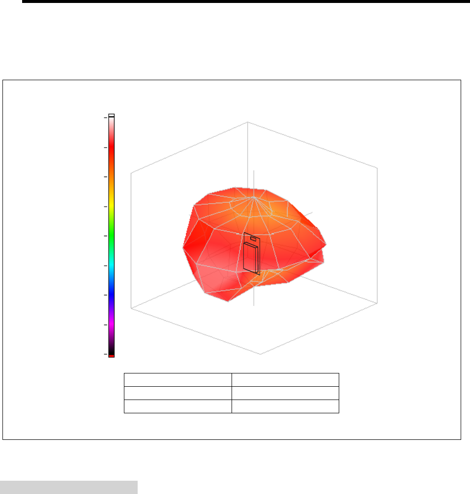
BM78SPPS5NC2 Ceramic Chip Antenna
The BM78SPPS5NC2 module contains an integral ceramic chip antenna. The antenna performance on
the module is shown in Figure 12-2.
FIGURE 12‐2: BM78SPPS5NC2 ANTENNA RADIATION PATTERN
Gain (dBi)
0.0
5.0
-5.0
-10.0
-15.0
-20.0
-25.0
-30.0
-35.0
X-axis
Y-axis
Z-axis
Frequency
2450 MHz
Max Gain
1.63 dBi
Efficiency
71.55%

13.0 Electrical Characteristics
Recommended Operating Conditions
Rating Min Typ Max
Storage temperature range -65ºC +25ºC +150ºC
Ambient Operating temperature range -20ºC +25ºC +70ºC
Relative Humidity (Operating) 10% 90%
Relative Humidity (Storage) 10% 90%
ESD
HBM ±2KV
MM 200V
HTOL
(*1)
1000 hrs
Supply voltage : BAT_IN 3.2V 4.3V
SW_BTN 1.7V 4.3V
LED1 3.6V
Reset
V
TH,res
threshold voltage
1.6V
IOH 12mA
IOL 12mA
VIL input logic levels low -0.3V 0.8V
VIH input logic levels high 2.0V 3.6V
VOL output logic levels low 0.4V
VOH output logic levels high 2.4V
RF TX mode 43 mA
RF RX mode 37 mA
1) HTOL life test condition : +125ºC , BAT_IN=4.2V, LDO33_O= 3.3V, LDO18_O=1.9V
1.8V LDO
(*1)(*2) Min Typ Max Unit
Operation Temperature -20 70 ℃
Input Voltage (V
in
)
(*3)
2.0 3.6 V
Output Current (V
IN
=3.0v/load regulation with
80m
V
drop
)
100
mA
Quiescent Current (V
in
<3.0V) 13 uA
1) With 1uF capacitors at LDO18_O as the condition of IP verification.
2) Output voltage can calibration by MP tool
3.3V LDO
(*1)(*2) Min Typ Max Unit
Operation Temperature -20 70 ℃
Input Voltage (V
in
) 3.2 4.3 V
Output Current (V
IN
=3.6v / load regulation with
100mV drop) 100 mA
Quiescent Current(V
IN
=3.6v) 150 uA
1) With 10uF capacitor at LDO33_O as the condition of IP verification
2) Output voltage can calibration by MP tool
PMU LDO
(*1)(*2) Min Typ Max Unit
Operation Temperature -20 70 ℃
Input Voltage (V
in
) 3.2 4.3 V
Output Current (VIN=3.6v / load regulation
with
0.3
mV drop
)
100 uA
Quiescent Current(VIN=3.6v) 120 uA
1) With 1uF capacitor at PMULDO_O as the condition of IP verification.
2) Output voltage can calibration by MP tool
SAR‐ADC and Battery Voltage Detector
Min Typ Max Unit
Operation Temperature -20 70 ℃
AVDD_SAR power supply
1.8
V
SAR_BAT(BAT_IN) 1.1 4.5 V
Resolution 10 bit

1) SAR_BAT is shorted to BAT_IN internally for battery voltage detection.
Intensity controllable LED driver
Min Typ Max Unit
Operation Temperature -20 70 ℃
Open-drain Voltage 3.6 V
Current Step 0.3
mA
Programmable Current Range 0 5 mA
Intensity control 16 step
Power down open-drain current 1 uA
Shutdown Current 1 uA
Operating Current (including bandgap) 1 mA
Shutdown Current 1 uA

14.0 Radio Characteristics:
Transmitter Performance (25℃
℃℃
℃)
Min Typ Max Bluetooth
specification
Unit
BDR power
2
-6 ~ +4
dBm EDR power 0 -6 ~ +4
LE power 2 -20 ~ +10
NOTE:
1) The RF Transmit power calibrated during production using MP Tool software and MT8852
Bluetooth Test equipment.
2) Test condition: VCC_RF= 1.80V, temperature=25 ºC.
Receiver Performance (25℃
℃℃
℃)
Basic Data Rate Min Typ Max Bluetooth
specification
Unit
BDR Sensitivity -90
≤-70 dBm
EDR 2M Sensitivity -90
EDR 3M Sensitivity -82
LE Sensitivity -92
NOTE:
1) Test condition: VCC_RF= 1.80V, temperature=25 ºC.

15.0 System Current Consumption
SUPPLY CONSUMPTION – CLASSIC
(1)
Parameter
Current
(avg.)
Units : mA
Current
Notes
Standb
y
mode
2.543
shut
down
mode
0.187
Connect
e
d
+
Sniff,
Master
(n
o
d
a
ta)
0.
541
N
o
dat
a
was
transmitted
Sniff interval = 500ms
Connect
e
d
+
Sniff,
Slave
(
no
data)
0.
551
N
o
dat
a
was
transmitted
Sniff interval = 500ms
Data,
Master
10.67
(Data
trans
mi
tted
at
1152
0
0
bps;
block
size=500)
Data,
Slave
14.87
(Data
trans
mi
tted
at
1152
0
0
bps;
block
size=500)
Note 1: Classic BR/EDR, RX_IND Function Enabled
2. The DATA from IS1678S-151
SUPPLY CONSUMPTION –LOW ENERGY
(1)
Parameter
Current
(avg.)
Units : mA
Notes
Shutdown
mode
0.13
LE fast advertising
1.21
LE fast advertising interval =100 ms
0.88
LE fast advertising interval = 160 ms
0.48
LE fast advertising interval = 500 ms
1.72
LE fast advertising interval = 100 ms +
B
eacon 100 ms
0.62
LE fast advertising interval = 500 ms +
B
eacon 500 ms
Reduced Power advertising
0.39
LE Reduced Power advertising
interval = 961 ms
1.00
LE Reduced Power advertising
interval = 961 ms+ Beacon 100 ms
0.51
LE Reduced Power advertising
interval = 961 ms +
B
eacon 500 ms
Connected (No data)
0.39
Connection interval = 1500 ms
0.43
Connection interval = 600 ms
Connected (iPhone6IC)
0.45
Connection interval = 500 ms
0.60
Connection interval = 200 ms
Connected (ICiPhone6)
6.6
Connection interval = 500 ms
7.0
Connection interval = 200 ms
Note 1. Only Low Energy, RX_IND Function Enabled
2. The DATA from IS1678S-151
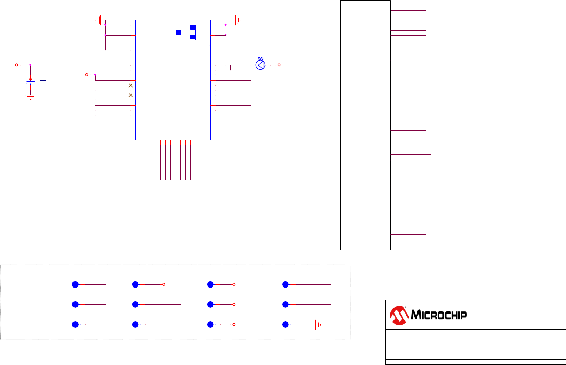
16.0 REFERENCE CIRCUIT
BM78 Reference Circuit
P3_7
P3_3
P3_1
P3_2
P3_4
P3_6
UART_RXD
UART_TXD
RST_N
P1_7
P0_5
P0_0
P2_0
EAN
P2_4
SW_BTN
VDD_IO
WAKEUP
P1_3
P1_2
P1_5
P0_4
LED1
LED-B
12
LDO33_O
BAT_IN
LDO33_O LDO33_0
FP1
FP-BM78SPPA
G
1
G
2
GND
3
BAT_IN
4
SW_BTN
5
LDO33_O
6
VDD_IO
7
LDO18_O
8
WAKEUP
9
PMULDO_O
10
P0_4
11
P1_5
12
P12 / SCL
13
P13 / SDA
14
P1_7
15
P0_5
16
P0_0
17
P2_0
18
P2_4
19
EAN
20
RST_N
21
GND 31
LED1 30
P3_7 29
P3_6 28
P3_4 27
P3_3 26
P3_2 25
P3_1 24
HCI_TXD 23
HCI_RXD 22
G33
G32
C1
10u/16V
BAT_I N
Bo a r d N a m e
Siz e
Tit le Rev
Da t e : S h e e t of
P/ N
MAIN CIRCUIT
1.0
BM78S REFERANCE CIRCUIT
Custom
2 4Friday , April 24, 2015
0222
5F, No.5, Industry E. Rd. VII, Hsinchu Science Park,
Hsinchu City 30078, Taiwan
TEL. 886-3-5778385
P3_4
P3_7
1
MCU
P3_1
P3_3
P3_2
UART_TXD
UART_RXD
P0_4
P1_5
P3_6
P0_5
1
Reset for I2C IC
1
Functional GPIO
RST_N
SW_BTN
WAKEUP
1
RST_N
1
WAKEUP
1
UART TXD / RXD
1
Status_IND
P1_7
1
UART CTS / RTS
1
SW_BTN
P0_0
TP2 TP-2
TP10TP-2
TP6 TP-2
TP3 TP-2
TP7 TP-2
TP5 TP-2
TP11TP-2
TP9 TP-2
TP13TP-2
SW_BTN
UART_RXD
EAN
P2_0
RST_N
1
Test PIN
BAT_IN
P2_4
UART_TXD
TP8 TP-2
TP4 TP-2
PMULDO_O
TP12TP-2
LDO18_O
LDO33_O

1.0 REGULATORY APPROVAL
This section outlines the regulatory information for the BM78SSPS5MC2 module for the following
countries:
• United States
• Canada
• Europe
• Australia
• Japan
• Korea
• Taiwan
• China
1.2 United States
The BM78SSPS5MC2 module has received Federal Communications Commission (FCC) CFR47
Telecommunications, Part 15 Subpart C “Intentional Radiators” modular approval in accordance with Part
15.212 Modular Transmitter approval. Modular approval allows the end user to integrate the BM78
module into a finished product without obtaining subsequent and separate FCC approvals for intentional
radiation, provided no changes or modifications are made to the module circuitry. Changes or
modifications could void the user’s authority to operate the equipment. The end user must comply with all
of the instructions provided by the Grantee, which indicate installation and/or operating conditions
necessary for compliance.
The finished product is required to comply with all applicable FCC equipment authorizations regulations,
requirements and equipment functions not associated with the transmitter module portion. For example,
compliance must be demonstrated to regulations for other transmitter components within the host
product; to requirements for unintentional radiators (Part 15 Subpart B “Unintentional Radiators”), such
as digital devices, computer peripherals, radio receivers, etc.; and to additional authorization requirements
for the non-transmitter functions on the transmitter module (i.e., Verification, or Declaration of
Conformity) (e.g., transmitter modules may also contain digital logic functions) as appropriate.
1.2.1 LABELING AND USER INFORMATION REQUIREMENTS
The BM78 module has been labeled with its own FCC ID number, and if the FCC ID is not visible when the
module is installed inside another device, then the outside of the finished product into which the module
is installed must also display a label referring to the enclosed module. This exterior label can use wording
as follows:
A user’s manual for the finished product should include the following statement:
Contains Transmitter Module FCC ID:
A8TBM78ABCDEFGH
or
Contains FCC ID: A8TBM78ABCDEFGH
This device complies with Part 15 of the FCC Rules. Operation is subject to the
following two conditions: (1) this device may not cause harmful interference,
and (2) this device must accept any interference received, including
interference that may cause undesired operation
PENDING

Additional information on labeling and user information requirements for Part 15 devices can be found in
KDB Publication 784748 available at the FCC Office of Engineering and Technology (OET) Laboratory
Division Knowledge Database (KDB) http://apps.fcc.gov/oetcf/kdb/index.cfm.
1.2.2 RF EXPOSURE
All transmitters regulated by FCC must comply with RF exposure requirements. KDB 447498 General RF
Exposure Guidance provides guidance in determining whether proposed or existing transmitting facilities,
operations or devices comply with limits for human exposure to Radio Frequency (RF) fields adopted by
the Federal Communications Commission (FCC).
From the FCC Grant: Output power listed is conducted. This grant is valid only when the module is sold to
OEM integrators and must be installed by the OEM or OEM integrators. This transmitter is restricted for
use with the specific antenna(s) tested in this application for Certification and must not be co-located or
operating in conjunction with any other antenna or transmitters within a host device, except in accordance
with FCC multi-transmitter product procedures.
1.2.3 HELPFUL WEB SITES
Federal Communications Commission (FCC): http://www.fcc.gov
FCC Office of Engineering and Technology (OET) Laboratory Division Knowledge Database (KDB):
http://apps.fcc.gov/oetcf/kdb/index.cfm
This equipment has been tested and found to comply with the limits for a
Class B digital device, pursuant to part 15 of the FCC Rules. These limits are
designed to provide reasonable protection against harmful interference in a
residential installation. This equipment generates, uses and can radiate radio
frequency energy, and if not installed and used in accordance with the
instructions, may cause harmful interference to radio communications.
However, there is no guarantee that interference will not occur in a particular
installation. If this equipment does cause harmful interference to radio or
television reception, which can be determined by turning the equipment off
and on, the user is encouraged to try to correct the interference by one or
more of the following measures:
• Reorient or relocate the receiving antenna.
• Increase the separation between the equipment and receiver.
• Connect the equipment into an outlet on a circuit different from that
to which the receiver is connected.
• Consult the dealer or an experienced radio/TV technician for help.

1.3 Canada
The BM78SPPS5MC2 module has been certified for use in Canada under Industry Canada (IC) Radio
Standards Specification (RSS) RSS-210 and RSS-Gen. Modular approval permits the installation of a module
in a host device without the need to recertify the device.
1.3.1 LABELING AND USER INFORMATION REQUIREMENTS
Labeling Requirements for the Host Device (from Section 3.2.1, RSS-Gen, Issue 3, December 2010): The
host device shall be properly labeled to identify the module within the host device.
The Industry Canada certification label of a module shall be clearly visible at all times when installed in the
host device, otherwise the host device must be labeled to display the Industry Canada certification
number of the module, preceded by the words “Contains transmitter module”, or the word “Contains”, or
similar wording expressing the same meaning, as follows:
User Manual Notice for License-Exempt Radio Apparatus (from Section 7.1.3 RSS-Gen, Issue 3, December
2010): User manuals for license-exempt radio apparatus shall contain the following or equivalent notice in
a conspicuous location in the user manual or alternatively on the device or both:
Contains transm
itter module IC: 12246A
-
BM7
8SPPS5M2
This device complies with Industry Canada license
-
exem
pt RSS standard(s).
Operation is subject to the following two conditions: (1) this device may not
cause interference, and (2) this device must accept any interference, including
interference that may cause undesired operation of the device.
Le présent appareil est conforme aux CNR d'Industrie Canada applicables aux
appareils radio exempts de licence. L'exploitation est autorisée aux deux
conditions suivantes: (1) l'appareil ne doit pas produire de brouillage, et (2)
l'utilisateur de l'appareil doit accepter tout brouillage radioélectrique subi,
même si le brouillage est susceptible d'en compromettre le fonctionnement.
PENDING
1.3.2 RF EXPOSURE
All transmitters regulated by IC must comply with RF exposure requirements listed in RSS-102 - Radio
Frequency (RF) Exposure Compliance of Radiocommunication Apparatus (All Frequency Bands).
(Get direct quote from Certificate and place here)
1.3.3 HELPFUL WEB SITES
Industry Canada: http://www.ic.gc.ca/
1.4 Europe
The BM78SPPS5MC2 module is an R&TTE Directive assessed radio module that is CE marked and has been
manufactured and tested with the intention of being integrated into a final product.
The BM78 module has been tested to R&TTE Directive 1999/5/EC Essential Requirements for Health and
Safety (Article (3.1(a)), Electromagnetic Compatibility (EMC) (Article 3.1(b)), and Radio (Article 3.2) and are
summarized in Table 3‐1: European Compliance Testing. A Notified Body Opinion has also been issued. All
test reports are available on the BM78 product web page at http://www.microchip.com/bm78.
The R&TTE Compliance Association provides guidance on modular devices in document Technical
Guidance Note 01 available at http://www.rtteca.com/html/download_area.htm.
1.4.1 LABELING AND USER INFORMATION REQUIREMENTS
The label on the final product which contains the BM77 module must follow CE marking requirements. The
R&TTE Compliance Association Technical Guidance Note 01 provides guidance on final product CE
marking.
1.4.2 ANTENNA REQUIREMENTS
From R&TTE Compliance Association document Technical Guidance Note 01:
Provided the integrator installing an assessed radio module with an integral or specific antenna
and installed in conformance with the radio module manufacturer’s installation instructions
requires no further evaluation under Article 3.2 of the R&TTE Directive and does not require
further involvement of an R&TTE Directive Notified Body for the final product. [Section 2.2.4]
The European Compliance Testing listed in Table 3‐1 was performed using the integral ceramic chip
antenna.
TABLE 3‐1: EUROPEAN COMPLIANCE TESTING
Certification
Standards
Article
Laboratory
Report Number
Date
Safety
EN
60950
-
1:2006+A11:2009+A1:2010
(3.1(a))
Health
EN 50371:2002
-
03
Note:
To maintain conformance to the testing listed in
Table 3
‐
1:
European Compliance Testing
, the
module shall be installed in accordance with the installation instructions in this data sheet and shall
not be modified.
When integrating a radio module into a completed product the integrator becomes the manufacturer
of the final product and is therefore responsible for demonstrating compliance of the final product
with the essential requirements of the R&TTE Directive.
PENDING

EMC
EN 301 489
-
1 V1.8.1 (2008
-
04)
(3.1(b))
EN 301 489
-
17 V2.1.1 (2009
-
05)
Radio
EN 300 328 V1.7.1 (2006
-
10)
(3.2)
Notified Body
Opinion
1.4.3 HELPFUL WEB SITES
A document that can be used as a starting point in understanding the use of Short Range Devices (SRD) in
Europe is the European Radio Communications Committee (ERC) Recommendation 70-03 E, which can be
downloaded from the European Radio Communications Office (ERO) at: http://www.ero.dk/.
Additional helpful web sites are:
• Radio and Telecommunications Terminal Equipment (R&TTE):
http://ec.europa.eu/enterprise/rtte/index_en.htm
• European Conference of Postal and Telecommunications Administrations (CEPT):
http://www.cept.org
• European Telecommunications Standards Institute (ETSI):
http://www.etsi.org
• European Radio Communications Office (ERO):
http://www.ero.dk
• The Radio and Telecommunications Terminal Equipment Compliance Association (R&TTE CA):
http://www.rtteca.com/
1.5 Australia
The Australia radio regulations do not provide a modular approval policy similar to the United States (FCC)
and Canada (IC). However, BM77 module RF transmitter test reports can be used in part to demonstrate
compliance in accordance with ACMA Radio communications “Short Range Devices” Standard 2004 (The
Short Range Devices standard calls up the AS/NZS 4268:2008 industry standard). The BM77 module test
reports can be used as part of the product certification and compliance folder. For more information on
the RF transmitter test reports, contact Microchip Technology Australia sales office.
To meet overall Australian final product compliance, the developer must construct a compliance folder
containing all relevant compliance test reports e.g. RF, EMC, electrical safety and DoC (Declaration of
Conformity) etc. It is the responsibility of the integrator to know what is required in the compliance folder
for ACMA compliance. All test reports are available on the BM78 product web page at
http://www.microchip.com. For more information on Australia compliance, refer to the Australian
Communications and Media Authority web site http://www.acma.gov.au/.
1.5.1 HELPFUL WEB SITES
The Australian Communications and Media Authority: www.acma.gov.au/.
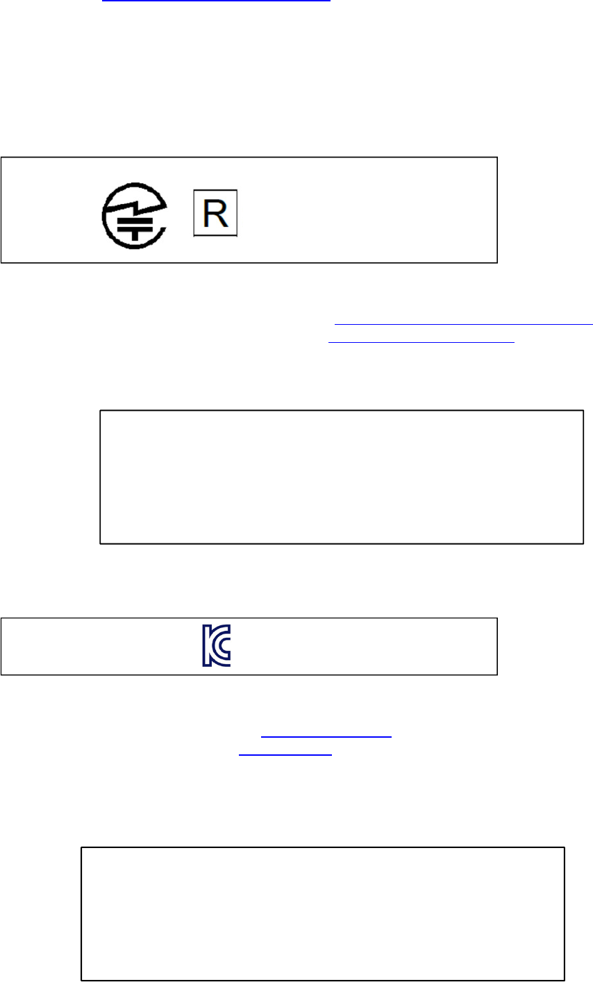
1.6 Japan
The BM78SPPS5MC2 module has received type certification and is labeled with its own technical
conformity mark and certification number as required to conform to the technical standards regulated by
the Ministry of Internal Affairs and Communications (MIC) of Japan pursuant to the Radio Act of Japan.
Integration of this module into a final product does not require additional radio certification provided
installation instructions are followed and no modifications of the module are allowed. Additional testing
may be required:
• If the host product is subject to electrical appliance safety (for example, powered from an AC
mains), the host product may require Product Safety Electrical Appliance and Material (PSE)
PENDING
PENDING
testing. The integrator should contact their conformance laboratory to determine if this testing is
required.
• There is an voluntary Electromagnetic Compatibility (EMC) test for the host product administered
by VCCI: http://www.vcci.jp/vcci_e/index.html
1.6.1 LABELING AND USER INFORMATION REQUIREMENTS
The label on the final product which contains the BM78 module must follow Japan marking requirements.
The integrator of the module should refer to the labeling requirements for Japan available at the Ministry
of Internal Affairs and Communications (MIC) website.
The BM78module is labeled with its own technical conformity mark and certification number. The final
product in which this module is being used must have a label referring to the type certified module inside:
1.6.2 HELPFUL WEB SITES
Ministry of Internal Affairs and Communications (MIC): http://www.tele.soumu.go.jp/e/index.htm
Association of Radio Industries and Businesses (ARIB): http://www.arib.or.jp/english/
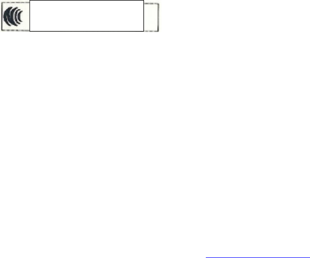
1.7 Korea
The BM78SPPS5MC2 module has received certification of conformity in accordance with the Radio Waves
Act. Integration of this module into a final product does not require additional radio certification provided
installation instructions are followed and no modifications of the module are allowed.
1.7.1 LABELING AND USER INFORMATION REQUIREMENTS
The label on the final product which contains the BM77 module must follow KC marking requirements. The
integrator of the module should refer to the labeling requirements for Korea available on the Korea
Communications Commission (KCC) website.
The BM78 module is labeled with its own KC mark. The final product requires the KC mark and certificate
number of the module:
1.7.2 HELPFUL WEB SITES
Korea Communications Commission (KCC): http://www.kcc.go.kr
National Radio Research Agency (RRA): http://rra.go.kr
1.8 Taiwan
The BM78SPPS5MC2 module has received compliance approval in accordance with the
Telecommunications Act. Customers seeking to use the compliance approval in their product should
contact Microchip Technology sales or distribution partners to obtain a Letter of Authority.
Integration of this module into a final product does not require additional radio certification provided
installation instructions are followed and no modifications of the module are allowed.
Contains transmitter module with certificate number:
(Number)
202-XXXXXX
PENDING
PENDING
1.8.1 LABELING AND USER INFORMATION REQUIREMENTS
The BM77 module is labeled with its own NCC mark and certificate number as below:
The user’s manual should contain below warning (for RF device) in traditional Chinese:
注意 !
依據 低功率電波輻射性電機管理辦法
第十二條 經型式認證合格之低功率射頻電機,非經許可,
公司、商號或使用者均不得擅自變更頻率、加大功率或變更原設計
之特性及功能。
第十四條 低功率射頻電機之使用不得影響飛航安全及干擾合法通信;
經發現有干擾現象時,應立即停用,並改善至無干擾時方得繼續使用。
前項合法通信,指依電信規定作業之無線電信。
低功率射頻電機須忍受合法通信或工業、科學及醫療用電波輻射性
電機設備之干擾。
1.8.2 HELPFUL WEB SITES
National Communications Commission (NCC): http://www.ncc.gov.tw
1.9 Other Regulatory Jurisdictions
Should other regulatory jurisdiction certification be required by the customer, or the customer need to
recertify the module for other reasons, a certification utility is available. For further regulatory
Certification Utility and documentation, contact ISSC Technologies Corp.
(Number)
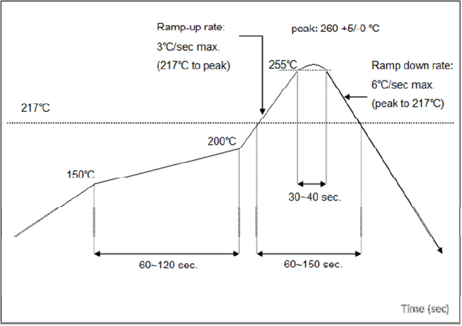
FIGURE 20-1: Reflow Profile
Standard : IPC/JEDEC J-STD-020
Condition :
Preheat
:
150~200
℃、
60~120 seconds
Average ramp-up rate (217
℃
to peak): 3
℃
/sec max.
Temperature maintained above 217
℃
: 60~150 seconds
Time within 5
℃
of peak temperature: 30 ~ 40 seconds.
Peak temperature
:
260 +5/-0
℃
Ramp-down rate (peak to 217
℃
) : 6
℃
/sec. max.
Time 25
℃
to peak temperature : 8 minutes max.
Cycle interval
:
5 minutes

Soldering Recommendations
Stereo module was assembled using standard lead-free reflow profile IPC/JEDEC J-STD-020.
The
module can be soldered to the main PCB using standard leaded and lead-free solder reflow profiles.
To
avoid damaging of the module, the recommendations are listed as follows:
•
Refer to Microchip Technology Application Note AN233 Solder Reflow Recommendation (DS00233)
for the
soldering reflow recommendations
•
Do not exceed peak temperature (TP) of 250 degree C
•
Refer to the solder paste data sheet for specific reflow profile recommendations
•
Use no-clean flux solder paste
•
Do not wash as moisture can be trapped under the shield
•
Use only one flow. If the PCB requires multiple flows, apply the module on the final flow.
ORDERING INFORMATION
TABLE 4‐1: ORDERING INFORMATION
Part Number
Description
BM7
8
SPPS
5N
C2
-
00
0
---
Bluetooth® 4.0 Dual Mode, Class 2, Surface Mount module with integral
antenna, with shield
BM7
8
SPP0
5N
C2
-
000
---
Bluetooth® 4.0 Dual Mode, Class 2, Surface Mount module, external
antenna, no shield

A.3.3 HELPFUL WEB SITES
A document that can be used as a starting point in understanding the use of Short Range
Devices (SRD)
in Europe is the European Radio Communications Committee (ERC)
Recommendation 70‐03 E, which can
be downloaded from the European Radio
Communications Office (ERO) at: http://www.ero.dk/.
Additional helpful web sites are:
• Radio and Telecommunications Terminal Equipment (R&TTE):
http://ec.europa.eu/enterprise/rtte/index_en.htm
• European Conference of Postal and Telecommunications Administrations (CEPT):
http://www.cept.org
• European Telecommunications Standards Institute (ETSI):
http://www.etsi.org
• European Radio Communications Office (ERO):
http://www.ero.dk
• The Radio and Telecommunications Terminal Equipment Compliance Association
(R&TTE CA):
http://www.rtteca.com/

Worldwide Sales and Service
AMERICAS
Corporate Office
2355 West Chandler Blvd.
Chandler, AZ 85224-6199
Tel: 480-792-7200
Fax: 480-792-7277
Technical Support:
http://www.microchip.com/
support
Web Address:
www.microchip.com
Atlanta
Duluth, GA
Tel: 678-957-9614
Fax: 678-957-1455
Austin, TX
Tel: 512-257-3370
Boston
Westborough, MA
Tel: 774-760-0087
Fax: 774-760-0088
Chicago
Itasca, IL
Tel: 630-285-0071
Fax: 630-285-0075
Cleveland
Independence, OH
Tel: 216-447-0464
Fax: 216-447-0643
Dallas
Addison, TX
Tel: 972-818-7423
Fax: 972-818-2924
Detroit
Novi, MI
Tel: 248-848-4000
Houston, TX
Tel: 281-894-5983
Indianapolis
Noblesville, IN
Tel: 317-773-8323
Fax: 317-773-5453
Los Angeles
Mission Viejo, CA
Tel: 949-462-9523
Fax: 949-462-9608
New York, NY
Tel: 631-435-6000
San Jose, CA
Tel: 408-735-9110
Canada - Toronto
Tel: 905-673-0699
Fax: 905-673-6509
ASIA/PACIFIC
Asia Pacific Office
Suites 3707-14, 37th Floor
Tower 6, The Gateway
Harbour City, Kowloon
Hong Kong
Tel: 852-2943-5100
Fax: 852-2401-3431
Australia - Sydney
Tel: 61-2-9868-6733
Fax: 61-2-9868-6755
China - Beijing
Tel: 86-10-8569-7000
Fax: 86-10-8528-2104
China - Chengdu
Tel: 86-28-8665-5511
Fax: 86-28-8665-7889
China - Chongqing
Tel: 86-23-8980-9588
Fax: 86-23-8980-9500
China - Hangzhou
Tel: 86-571-8792-8115
Fax: 86-571-8792-8116
China - Hong Kong SAR
Tel: 852-2943-5100
Fax: 852-2401-3431
China - Nanjing
Tel: 86-25-8473-2460
Fax: 86-25-8473-2470
China - Qingdao
Tel: 86-532-8502-7355
Fax: 86-532-8502-7205
China - Shanghai
Tel: 86-21-5407-5533
Fax: 86-21-5407-5066
China - Shenyang
Tel: 86-24-2334-2829
Fax: 86-24-2334-2393
China - Shenzhen
Tel: 86-755-8864-2200
Fax: 86-755-8203-1760
China - Wuhan
Tel: 86-27-5980-5300
Fax: 86-27-5980-5118
China - Xian
Tel: 86-29-8833-7252
Fax: 86-29-8833-7256
China - Xiamen
Tel: 86-592-2388138
Fax: 86-592-2388130
China - Zhuhai
Tel: 86-756-3210040
Fax: 86-756-3210049
ASIA/PACIFIC
India - Bangalore
Tel: 91-80-3090-4444
Fax: 91-80-3090-4123
India - New Delhi
Tel: 91-11-4160-8631
Fax: 91-11-4160-8632
India - Pune
Tel: 91-20-3019-1500
Japan - Osaka
Tel: 81-6-6152-7160
Fax: 81-6-6152-9310
Japan - Tokyo
Tel: 81-3-6880- 3770
Fax: 81-3-6880-3771
Korea - Daegu
Tel: 82-53-744-4301
Fax: 82-53-744-4302
Korea - Seoul
Tel: 82-2-554-7200
Fax: 82-2-558-5932 or
82-2-558-5934
Malaysia - Kuala Lumpur
Tel: 60-3-6201-9857
Fax: 60-3-6201-9859
Malaysia - Penang
Tel: 60-4-227-8870
Fax: 60-4-227-4068
Philippines - Manila
Tel: 63-2-634-9065
Fax: 63-2-634-9069
Singapore
Tel: 65-6334-8870
Fax: 65-6334-8850
Taiwan - Hsin Chu
Tel: 886-3-5778-366
Fax: 886-3-5770-955
Taiwan - Kaohsiung
Tel: 886-7-213-7830
Taiwan - Taipei
Tel: 886-2-2508-8600
Fax: 886-2-2508-0102
Thailand - Bangkok
Tel: 66-2-694-1351
Fax: 66-2-694-1350
EUROPE
Austria - Wels
Tel: 43-7242-2244-39
Fax: 43-7242-2244-393
Denmark - Copenhagen
Tel: 45-4450-2828
Fax: 45-4485-2829
France - Paris
Tel: 33-1-69-53-63-20
Fax: 33-1-69-30-90-79
Germany - Dusseldorf
Tel: 49-2129-3766400
Germany - Munich
Tel: 49-89-627-144-0
Fax: 49-89-627-144-44
Germany - Pforzheim
Tel: 49-7231-424750
Italy - Milan
Tel: 39-0331-742611
Fax: 39-0331-466781
Italy - Venice
Tel: 39-049-7625286
Netherlands - Drunen
Tel: 31-416-690399
Fax: 31-416-690340
Poland - Warsaw
Tel: 48-22-3325737
Spain - Madrid
Tel: 34-91-708-08-90
Fax: 34-91-708-08-91
Sweden - Stockholm
Tel: 46-8-5090-4654
UK - Wokingham
Tel: 44-118-921-5800
Fax: 44-118-921-5820