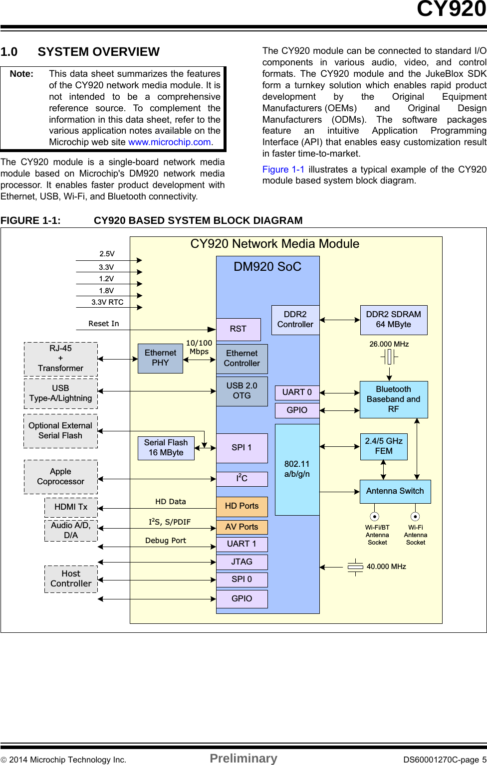
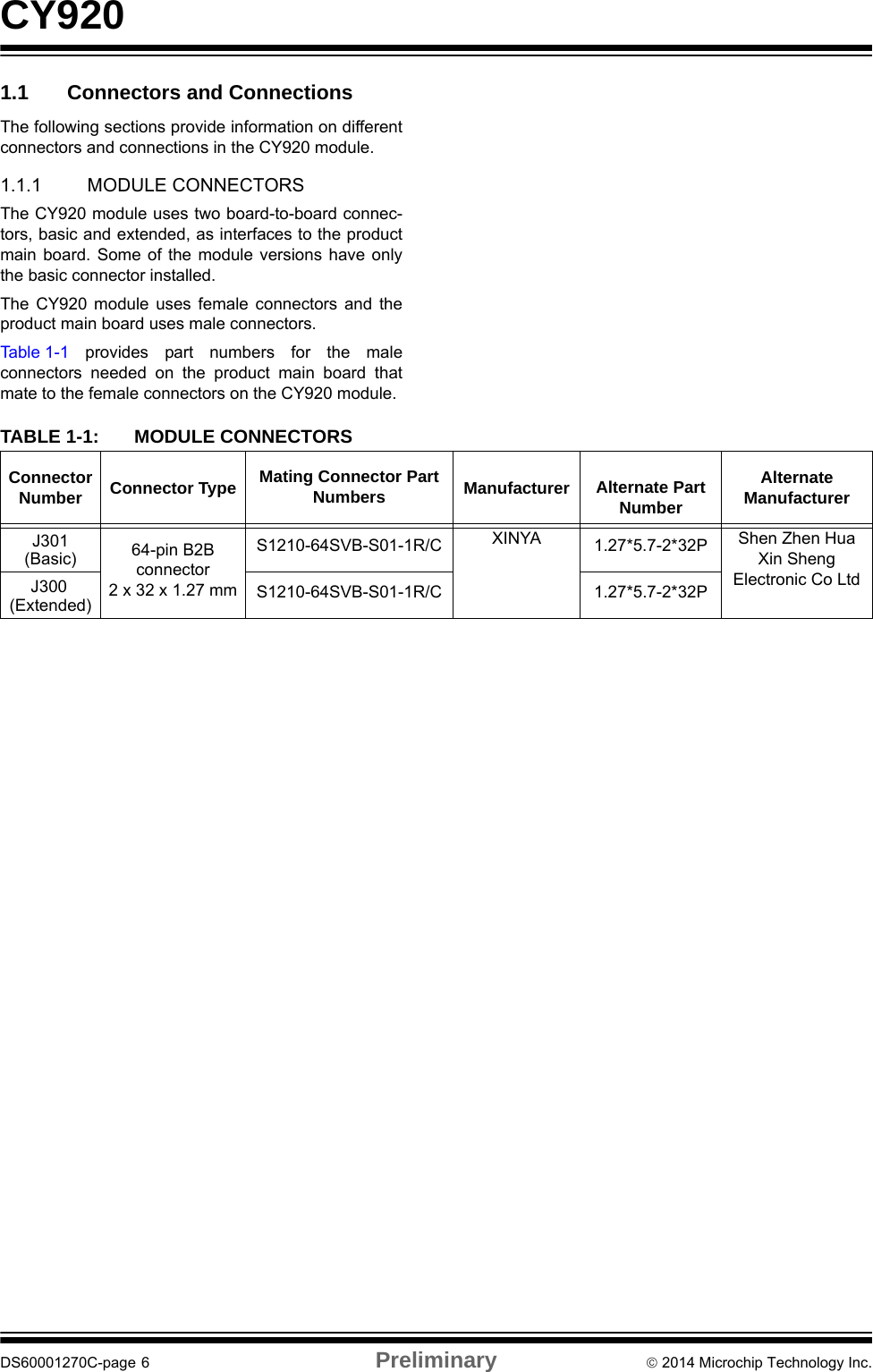
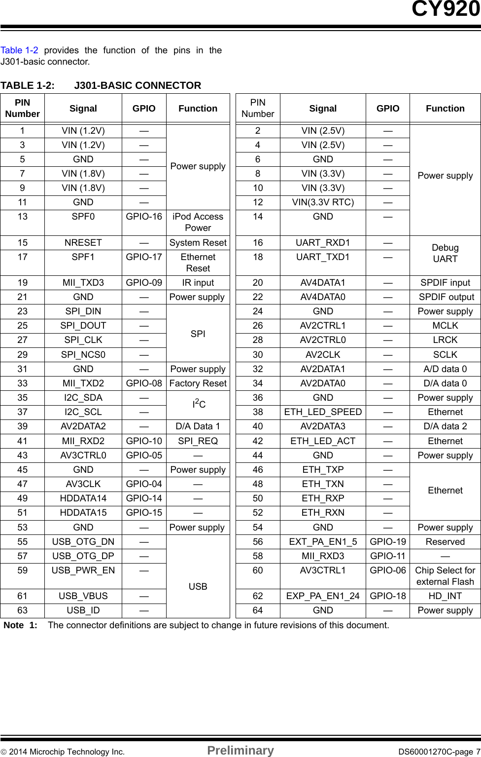
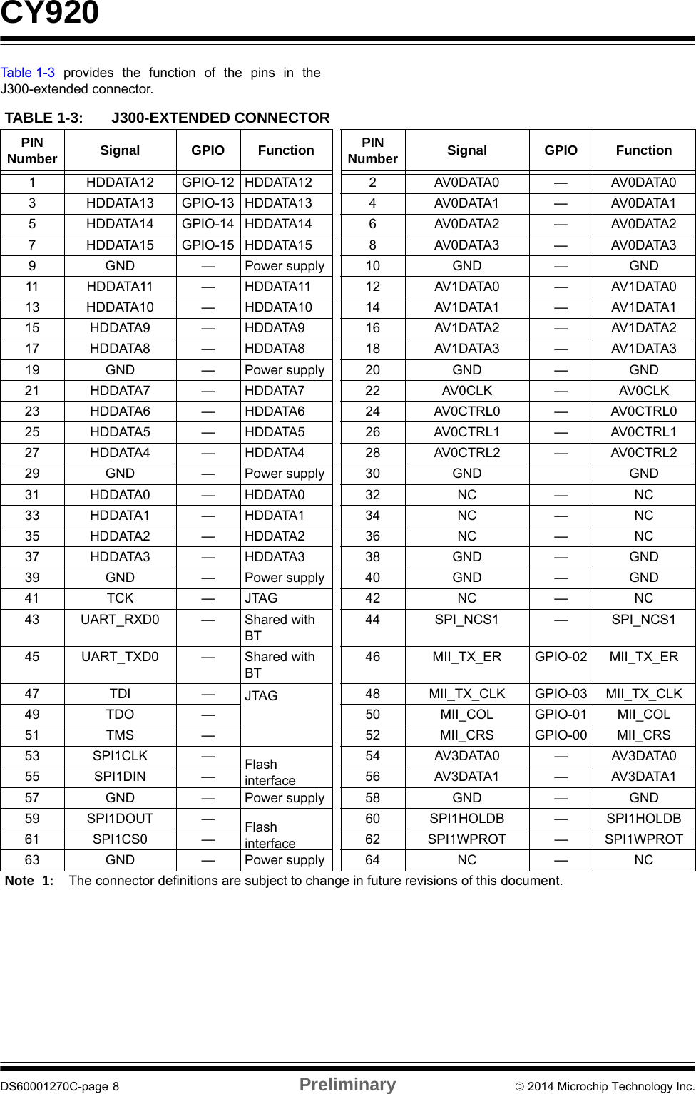
MICROCHIP TECHNOLOGY CY92024C Network Media Module User Manual Network Media Module
MICROCHIP TECHNOLOGY INC. Network Media Module Network Media Module
UserManual.wiki
>
MICROCHIP TECHNOLOGY
>
CY92024C User Manual
>
User Manual I
Contents
1.
User Manual I
2.
User Manual II
User Manual I
Navigation menu
Upload a User Manual
Namespaces
Wiki Guide
HTML
PDF
Info
Views
User Manual
Discussion / Help
Navigation


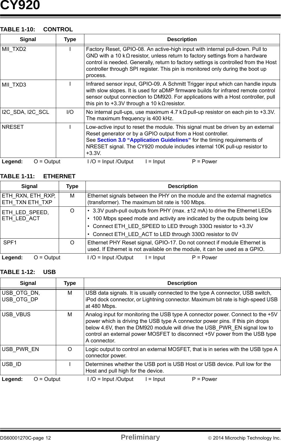
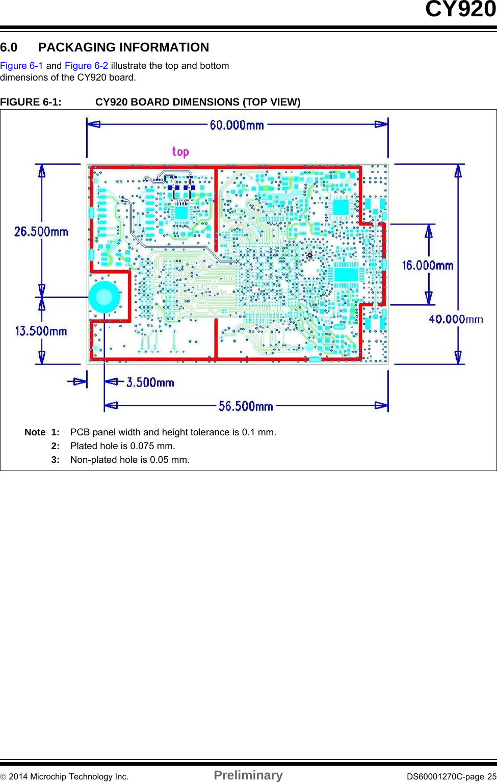
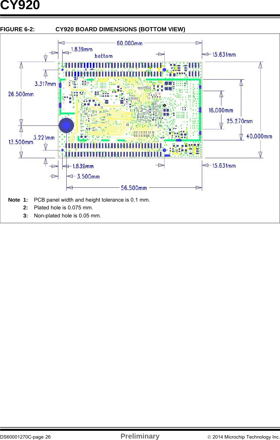
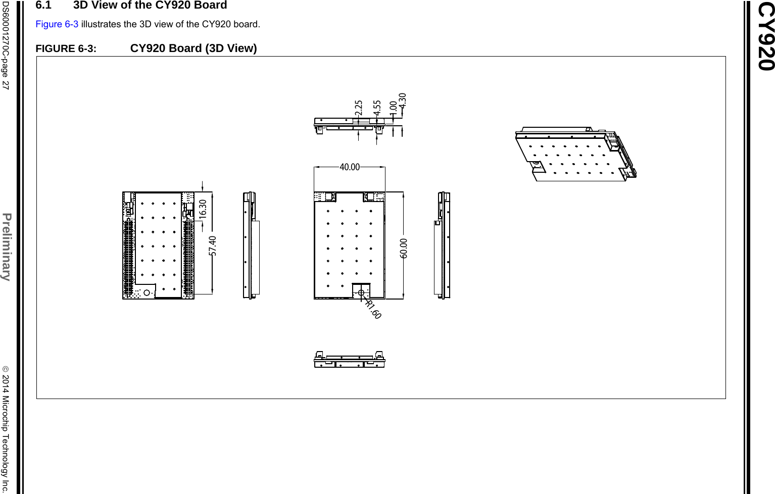
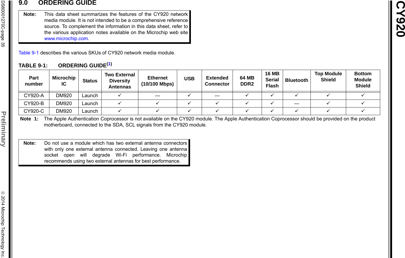
![© 2014 Microchip Technology Inc. Preliminary DS60001270C-page 13CY920TABLE 1-13: JTAGTABLE 1-14: VIDEOTABLE 1-15: GPIO (MISCELLANEOUS)Microchip has a set of example schematics that showshow the external circuitry is typically connected to themodule. Please contact Microchip sales team for anyrelated documents or for any assistance.Signal Type DescriptionTMS,TCK,TDI, TDO I/O JTAG ports for the DM920 SoC. Do not connect these pins.Legend: O = Output I /O = Input /Output I = Input P = Power Signal Type DescriptionAV0CLK O HD ClockAV0CTRL0 O HD HSYNCAV0CTRL1 O HD VSYNCAV0CTRL2 O HD data enable, GPIO-07. This GPIO is available if HD interface is not used.HDDATA [15:0] O Lower 16 bits of HD video dataAV0DATA [3:0] O HDDATA [19:16]AV1DATA [3:0] O HDDATA [23:20]Legend: O = Output I /O = Input /Output I = Input P = Power Signal Type DescriptionMII_CRS, MII_COL, MII_TX_ER,MII_TXCLKI/O GPIO-00, 01, 02, 03. It is used for Bluetooth control signals. For a non-BT module, these signals can be used for other functions.AV3CLK I/O GPIO-04, see Note 1AV3CTRL0 I/O GPIO-05, see Note 1MII_RXD3 I/O GPIO-11, see Note 1HDDATA12 I/O GPIO-12, see Note 2HDDATA13 I/O GPIO-13, see Note 2HDDATA14 I/O GPIO-14, see Note 2HDDATA15 I/O GPIO-15, see Note 2SPF0 I/O GPIO-16, HD_INT (for systems with HDMI transmitter)EXT_PA_EN1_5 I/O GPIO-18, FEM BSELEXT_PA_EN1_24 I/O GPIO-19, see Note 1Legend: O = Output I /O = Input /Output I = Input P = Power Note 1: These GPIOs are available.2: These GPIOs are available if HD interface is not used.](https://usermanual.wiki/MICROCHIP-TECHNOLOGY/CY92024C.User-Manual-I/User-Guide-2322212-Page-13.png)