MICROCHIP TECHNOLOGY CY92024C Network Media Module User Manual Network Media Module
MICROCHIP TECHNOLOGY INC. Network Media Module Network Media Module
Contents
- 1. User Manual I
- 2. User Manual II
User Manual I

© 2014 Microchip Technology Inc. Preliminary DS60001270C-page 1
CY920
Operating Conditions
• 3.3V, 2.5V, 1.8V, 1.2V supply voltage
• Operating frequency up to 400 MHz
• Operating temperature: 0ºC to 70ºC
Features
• Audio networking system on a small footprint
module
•Wi-Fi
® certified 802.11 a/b/g/n
• Integrated Ethernet + USB 2.0 OTG
• Optional Bluetooth® v2.1 + EDR
• Diversity enabled external antenna connectors
• Glueless audio, video, and control ports
• FCC certification is planned for production version
• Ideal for enabling network and USB audio playback
for iPod
®
docks, audio systems, AV receivers,
active speaker systems, internet radios, network
playback adapters
WLAN
• Integrated 802.11 a/b/g/n MAC, Baseband
Processor (BBP) and radio frequency (RF)
transceiver
• Wi-Fi certified 802.11 a/b/g/n supporting both
2.4 GHz and 5 GHz bands
• On-chip wideband sniffer which enables
applications that benefit from efficient interference
management algorithms
• 1x1 dual band with Tx and Rx antenna diversity
• Supports Wi-Fi Direct®
• Two Ultra Small Miniature RF Connector (U.FL)
type external antenna connectors
Bluetooth (Optional)
• Compliant with Bluetooth (BT) v2.1 + EDR
specification
• A2DP and AVRCP profiles
• WLAN and Bluetooth co-existence using Packet
Traffic Arbitration (PTA) and Adaptive Frequency
Hopping (AFH)
• Utilizes same antenna as Wi-Fi system
• Supports Class 2 power output
• Low-power consumption
Memory Interfaces
• 16 MB on-board serial Flash memory
• 64 MB on-board DDR2 SDRAM
• Off-board serial Flash memory via extended
connector
Communication Interfaces
• 10/100 Mbps Ethernet support with Ethernet PHY
on-board
• USB 2.0 OTG with integrated PHY
• Serial Peripheral Interface (SPI), Inter-Integrated
Circuit™ (I2C™), Universal Asynchronous
Receiver Transmitter (UART) peripheral ports
• 3.3V tolerance on all digital IOs (GPIO, I2S,
SPDIF, SPI, UART, HDMI)
Audio and Graphics Interface
•I
2S support with external Digital-to-Analog
Converter (DAC)/Power Amplifier (PA)
• Built-in Digital Signal Processor (DSP) with dual
core 300 MHz each
• HDMI support with in-built 24-bit HD port and
external HDMI transmitter
• Supports analog video (composite, component
and S-Video) using external video encoder
Input/Output
• General Purpose Input Outputs (GPIOs) for
different Stock Keeping Units (SKUs):
- CY920-A: 11 GPIOs
- CY920-B: 13 GPIOs
- CY920-C: 9 GPIOs
Applications
• JukeBlox®: DLNA™, AirPlay® Speaker, network
audio DMR/ DMP, Internet radio, mini/micro
system
• Audio Video Receivers (AVR)
• Sound Bars
• PC OEM, TV and gaming consoles
• Operating as an access point (Wi-Fi Direct Host)
NETWORK MEDIA MODULE

CY920
DS60001270C-page 2 Preliminary © 2014 Microchip Technology Inc.
NOTES:

© 2014 Microchip Technology Inc. Preliminary DS60001270C-page 3
CY920
Table of Contents
System Overview .................................................................................................................................................................................. 5
CY920 Board Layout and Features .................................................................................................................................................... 15
Application Guidelines ........................................................................................................................................................................ 19
Wi-Fi Specification .............................................................................................................................................................................. 21
Bluetooth Specifications ...................................................................................................................................................................... 23
Packaging Information ........................................................................................................................................................................ 25
Electrical Characteristics ..................................................................................................................................................................... 29
Regulatory Compliance and Quality ................................................................................................................................................... 33
Ordering Guide ................................................................................................................................................................................... 35
Appendix A: Certification Notices ........................................................................................................................................................ 37
Appendix B: Revision History .............................................................................................................................................................. 39
The Microchip Web Site ...................................................................................................................................................................... 41
Customer Change Notification Service ............................................................................................................................................... 41
Customer Support ............................................................................................................................................................................... 41
TO OUR VALUED CUSTOMERS
It is our intention to provide our valued customers with the best documentation possible to ensure successful use of your Microchip
products. To this end, we will continue to improve our publications to better suit your needs. Our publications will be refined and
enhanced as new volumes and updates are introduced.
If you have any questions or comments regarding this publication, please contact the Marketing Communications Department via
E-mail at docerrors@microchip.com or fax the Reader Response Form in the back of this data sheet to (480) 792-4150. We
welcome your feedback.
Most Current Data Sheet
To obtain the most up-to-date version of this data sheet, please register at our Worldwide Web site at:
http://www.microchip.com
You can determine the version of a data sheet by examining its literature number found on the bottom outside corner of any page.
The last character of the literature number is the version number, (e.g., DS30000000A is version A of document DS30000000).
Errata
An errata sheet, describing minor operational differences from the data sheet and recommended workarounds, may exist for current
devices. As device/documentation issues become known to us, we will publish an errata sheet. The errata will specify the revision
of silicon and revision of document to which it applies.
To determine if an errata sheet exists for a particular device, please check with one of the following:
• Microchip’s Worldwide Web site; http://www.microchip.com
• Your local Microchip sales office (see last page)
When contacting a sales office, please specify which device, revision of silicon and data sheet (include literature number) you are
using.
Customer Notification System
Register on our web site at www.microchip.com to receive the most current information on all of our products.

CY920
DS60001270C-page 4 Preliminary © 2014 Microchip Technology Inc.
NOTES:
© 2014 Microchip Technology Inc. Preliminary DS60001270C-page 5
CY920
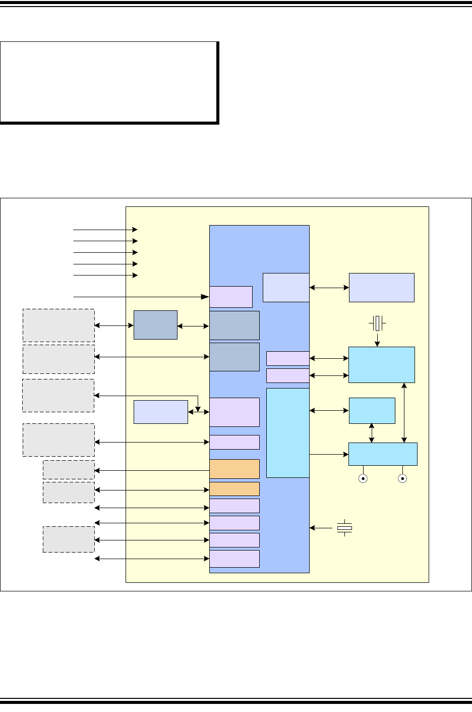
1.0 SYSTEM OVERVIEW
The CY920 module is a single-board network media
module based on Microchip's DM920 network media
processor. It enables faster product development with
Ethernet, USB, Wi-Fi, and Bluetooth connectivity.
The CY920 module can be connected to standard I/O
components in various audio, video, and control
formats. The CY920 module and the JukeBlox SDK
form a turnkey solution which enables rapid product
development by the Original Equipment
Manufacturers (OEMs) and Original Design
Manufacturers (ODMs). The software packages
feature an intuitive Application Programming
Interface (API) that enables easy customization result
in faster time-to-market.
Figure 1-1 illustrates a typical example of the CY920
module based system block diagram.
FIGURE 1-1: CY920 BASED SYSTEM BLOCK DIAGRAM
Note: This data sheet summarizes the features
of the CY920 network media module. It is
not intended to be a comprehensive
reference source. To complement the
information in this data sheet, refer to the
various application notes available on the
Microchip web site www.microchip.com.
Ethernet
PHY
DM920 SoC
DDR2 SDRAM
64 MByte
DDR2
Controller
USB 2.0
OTG
GPIO
40.000 MHz
Serial Flash
16 MByte
2.4/5 GHz
FEM
802.11
a/b/g/n
Ethernet
Controller
UART 1
3.3V RTC
CY920 Network Media Module
1.2V
Wi-Fi/BT
Antenna
Socket
1.8V
SPI 1
I2C
JTAG
RST
Reset In
AV Ports
SPI 0
Wi-Fi
Antenna
Socket
2.5V
I2S, S/PDIF
Bluetooth
Baseband and
RF
UART 0
GPIO
3.3V
HD Ports
HD Data
Apple
Coprocessor
Optional External
Serial Flash
Host
Controller
RJ-45
+
Transformer
USB
Type-A/Lightning
HDMI Tx
Audio A/D,
D/A
10/100
Mbps
Debug Port
Antenna Switch
26.000 MHz

CY920
DS60001270C-page 6 Preliminary © 2014 Microchip Technology Inc.
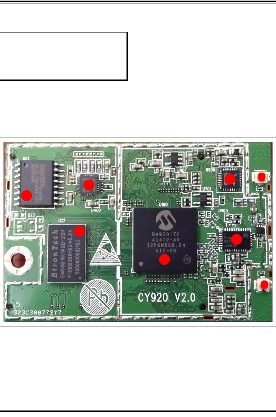
1.1 Connectors and Connections
The following sections provide information on different
connectors and connections in the CY920 module.
1.1.1 MODULE CONNECTORS
The CY920 module uses two board-to-board connec-
tors, basic and extended, as interfaces to the product
main board. Some of the module versions have only
the basic connector installed.
The CY920 module uses female connectors and the
product main board uses male connectors.
Table 1-1 provides part numbers for the male
connectors needed on the product main board that
mate to the female connectors on the CY920 module.
TABLE 1-1: MODULE CONNECTORS
Connector
Number Connector Type Mating Connector Part
Numbers Manufacturer Alternate Part
Number
Alternate
Manufacturer
J301
(Basic) 64-pin B2B
connector
2 x 32 x 1.27 mm
S1210-64SVB-S01-1R/C XINYA 1.27*5.7-2*32P Shen Zhen Hua
Xin Sheng
Electronic Co Ltd
J300
(Extended) S1210-64SVB-S01-1R/C 1.27*5.7-2*32P
© 2014 Microchip Technology Inc. Preliminary DS60001270C-page 7
CY920
Table 1-2 provides the function of the pins in the
J301-basic connector.
TABLE 1-2: J301-BASIC CONNECTOR
PIN
Number Signal GPIO Function PIN
Number Signal GPIO Function
1 VIN (1.2V) —
Power supply
2 VIN (2.5V) —
Power supply
3 VIN (1.2V) — 4 VIN (2.5V) —
5GND— 6 GND —
7 VIN (1.8V) — 8 VIN (3.3V) —
9 VIN (1.8V) — 10 VIN (3.3V) —
11 GND — 12 VIN(3.3V RTC) —
13 SPF0 GPIO-16 iPod Access
Power
14 GND —
15 NRESET — System Reset 16 UART_RXD1 — Debug
UART
17 SPF1 GPIO-17 Ethernet
Reset
18 UART_TXD1 —
19 MII_TXD3 GPIO-09 IR input 20 AV4DATA1 — SPDIF input
21 GND — Power supply 22 AV4DATA0 — SPDIF output
23 SPI_DIN —
SPI
24 GND — Power supply
25 SPI_DOUT — 26 AV2CTRL1 — MCLK
27 SPI_CLK — 28 AV2CTRL0 — LRCK
29 SPI_NCS0 — 30 AV2CLK — SCLK
31 GND — Power supply 32 AV2DATA1 — A/D data 0
33 MII_TXD2 GPIO-08 Factory Reset 34 AV2DATA0 — D/A data 0
35 I2C_SDA — I2C36 GND — Power supply
37 I2C_SCL — 38 ETH_LED_SPEED — Ethernet
39 AV2DATA2 — D/A Data 1 40 AV2DATA3 — D/A data 2
41 MII_RXD2 GPIO-10 SPI_REQ 42 ETH_LED_ACT — Ethernet
43 AV3CTRL0 GPIO-05 — 44 GND — Power supply
45 GND — Power supply 46 ETH_TXP —
Ethernet
47 AV3CLK GPIO-04 — 48 ETH_TXN —
49 HDDATA14 GPIO-14 — 50 ETH_RXP —
51 HDDATA15 GPIO-15 — 52 ETH_RXN —
53 GND — Power supply 54 GND — Power supply
55 USB_OTG_DN —
USB
56 EXT_PA_EN1_5 GPIO-19 Reserved
57 USB_OTG_DP — 58 MII_RXD3 GPIO-11 —
59 USB_PWR_EN — 60 AV3CTRL1 GPIO-06 Chip Select for
external Flash
61 USB_VBUS — 62 EXP_PA_EN1_24 GPIO-18 HD_INT
63 USB_ID — 64 GND — Power supply
Note 1: The connector definitions are subject to change in future revisions of this document.
CY920
DS60001270C-page 8 Preliminary © 2014 Microchip Technology Inc.
Table 1-3 provides the function of the pins in the
J300-extended connector.
TABLE 1-3: J300-EXTENDED CONNECTOR
PIN
Number Signal GPIO Function PIN
Number Signal GPIO Function
1 HDDATA12 GPIO-12 HDDATA12 2 AV0DATA0 — AV0DATA0
3 HDDATA13 GPIO-13 HDDATA13 4 AV0DATA1 — AV0DATA1
5 HDDATA14 GPIO-14 HDDATA14 6 AV0DATA2 — AV0DATA2
7 HDDATA15 GPIO-15 HDDATA15 8 AV0DATA3 — AV0DATA3
9 GND — Power supply 10 GND — GND
11 HDDATA11 — HDDATA11 12 AV1DATA0 — AV1DATA0
13 HDDATA10 — HDDATA10 14 AV1DATA1 — AV1DATA1
15 HDDATA9 — HDDATA9 16 AV1DATA2 — AV1DATA2
17 HDDATA8 — HDDATA8 18 AV1DATA3 — AV1DATA3
19 GND — Power supply 20 GND — GND
21 HDDATA7 — HDDATA7 22 AV0CLK — AV0CLK
23 HDDATA6 — HDDATA6 24 AV0CTRL0 — AV0CTRL0
25 HDDATA5 — HDDATA5 26 AV0CTRL1 — AV0CTRL1
27 HDDATA4 — HDDATA4 28 AV0CTRL2 — AV0CTRL2
29 GND — Power supply 30 GND GND
31 HDDATA0 — HDDATA0 32 NC — NC
33 HDDATA1 — HDDATA1 34 NC — NC
35 HDDATA2 — HDDATA2 36 NC — NC
37 HDDATA3 — HDDATA3 38 GND — GND
39 GND — Power supply 40 GND — GND
41 TCK — JTAG 42 NC — NC
43 UART_RXD0 — Shared with
BT
44 SPI_NCS1 — SPI_NCS1
45 UART_TXD0 — Shared with
BT
46 MII_TX_ER GPIO-02 MII_TX_ER
47 TDI — JTAG 48 MII_TX_CLK GPIO-03 MII_TX_CLK
49 TDO — 50 MII_COL GPIO-01 MII_COL
51 TMS — 52 MII_CRS GPIO-00 MII_CRS
53 SPI1CLK — Flash
interface
54 AV3DATA0 — AV3DATA0
55 SPI1DIN — 56 AV3DATA1 — AV3DATA1
57 GND — Power supply 58 GND — GND
59 SPI1DOUT — Flash
interface
60 SPI1HOLDB — SPI1HOLDB
61 SPI1CS0 — 62 SPI1WPROT — SPI1WPROT
63 GND — Power supply 64 NC — NC
Note 1: The connector definitions are subject to change in future revisions of this document.

© 2014 Microchip Technology Inc. Preliminary DS60001270C-page 9
CY920
Table 1-4 provides the GPIO assignment on the CY920
module.
TABLE 1-4: CY920 GPIO MAPPING
1.1.2 ANTENNA CONNECTOR
In the CY920 module two external antenna sockets are
used to enable diversity operation. During the diversity
operation, the firmware selects one antenna at a time
through the on-board Tx/Rx diversity RF switch.
The surface-mounted antenna socket used in the
CY920 module is Ultra Small Surface Mount Coaxial
(U.FL) type.
GPIO
Number DM920 Pin Name Connected To Assigned Function
0 MIICRS BT/extended connector WLAN_ACTIVE
1 MIICOL BT/extended connector BT_PRIORITY
2 MIITXER BT/extended connector BT_ACTIVE
3 MIITXCLK BT/extended connector BT_LDO_ON
4 AV3CLK Basic connector Available
5 AV3CTRL0 Basic connector Available
6 AV3CTRL1 Basic connector Chip select for expansion Flash
7 AV0CTRL2 Extended connector Available
8 MIITXD2 Basic connector Factory Reset
9 MIITXD3 Basic connector IR input
10 MIIRXD2 Basic connector SPI_REQ for Host controller
11 MIIRXD3 Basic connector Available
12 HDDATA12 Extended connector Available
13 HDDATA13 Extended connector Available
14 HDDATA14 Extended connector Available
15 HDDATA15 Extended connector Available
16 SPF0 Basic connector HD_INT
17 SPF1 Basic connector Ethernet Reset
18 EXT_PA_EN1_5 Basic connector FEM BSEL
19 EXT_PA_EN1_24 Basic connector Available
Note 1: The GPIO assignments are subject to change in future revisions of this document.
Note: Do not use the CY920 module that has
two external antenna sockets with only
one external antenna connected. This will
degrade the Wi-Fi or BT performance.
CY920
DS60001270C-page 10 Preliminary © 2014 Microchip Technology Inc.
1.2 Pin Description
Table 1-5 through Tab l e 1 - 1 5 provide an overview of
the important control and interface signals. It also
covers pinouts and signal names.
TABLE 1-5: POWER
TABLE 1-6: SERIAL PERIPHERAL INTERFACE (SPI)
TABLE 1-7: SPI FLASH INTERFACE
Signal Type Description
3.3V P Power input +3.3V
1.2V P Power input +1.2V
1.8V P Power input +1.8V
2.5V P Power input +2.5V
3.3V RTC P Power input +3.3V for Real-Time Clock (RTC). Power can be provided by battery or
external Supercap.
GND P Ground (GND) connection for power supply, signal returns and shielding
Legend: O = Output I /O = Input /Output I = Input P = Power
Signal Type Description
SPI_DOUT O SPI data from DM920 to Host controller
SPI_DIN I SPI data from Host controller to DM920
SPI_CLK I SPI clock from Host controller to DM920 (maximum recommended
frequency is 2 MHz and typical frequency is 1 MHz, see Note 1)
SPI_NCS0 I SPI Chip Select from Host controller to DM920
MII_RXD2 O • This GPIO signal is used as SPI_REQ (SPI request signal) from DM920 to
Host controller for eDMP applications.
• Logic 1 indicates there is an SPI message waiting to be read. The Host
controller should start the SPI clock and read any changed registers.
• Logic 0 indicates that all changed register messages have been read and the
message buffer is empty.
Legend: O = Output I /O = Input /Output I = Input P = Power
Note 1: For SPI timing diagram for eDMP applications, refer to “MCHP-JB -
Device_Control_Protocol_Registers_v_6_5” or later version. For detailed setup and hold timing details,
refer to the “DM920 Data Sheet” (DS60001278).
Signal Type Description
SPI1CS0 O Chip Select input for on-board Flash
AV3CTRL1 (GPIO6) O Chip Select for external Flash. For more information on how to connect
and access external Flash, refer to the Chapter 18. External Flash
Interface chapter in the “JukeBlox® Technology 4.X SDK User's Guide”
(DS70005181).
SPI1CLK O Clock signal to drive serial Flash
SPI1DIN I Data line from Flash output to DM920 input
SPI1DOUT O Data line from DM920 output to Flash input
SPI1HOLDB O Serial Flash control input
SPI1WPROT O Write protect input to serial Flash
Legend: O = Output I /O = Input /Output I = Input P = Power

© 2014 Microchip Technology Inc. Preliminary DS60001270C-page 11
CY920
TABLE 1-8: UNIVERSAL ASYNCHRONOUS RECEIVER TRANSMITTER (UART)
TABLE 1-9: AUDIO
Signal Type Description
UART_RXD1 I UART1 input to the DM920, used for shell access. Microchip recommends
providing a connection to an external RS-232 transceiver and a DB9 connector to
connect to a PC COM port. This connection can be used for the product
development debugging, module programming control on the product
manufacturing line, and module control during certification procedures.
UART_TXD1 O UART1 output from the DM920, used for shell access. Microchip recommends
providing a connection to an external RS-232 transceiver and a DB9 connector to
connect to a PC COM port. This connection can be used for the product
development debugging, module programming control on the product
manufacturing line, and module control during certification procedures.
UART_RXD0 I UART0 input, used for Bluetooth (BT) in BT SKU. It can be used as an additional
UART in non-BT SKU.
UART_TXD0 O UART0 output, used for Bluetooth in case of BT SKU. It can be used as an
additional UART in non-BT SKU
Legend: O = Output I /O = Input /Output I = Input P = Power
Signal Type Description
AV2DATA0
AV2DATA2
AV2DATA3
OI
2S or left justified audio data output. It is typically connected to an external D/A
converter input or an external DSP for further audio processing.
AV2DATA0 is used for the main left and right channel audio output data. AV2DATA2
and AV2DATA3 may be used for surround sound rear channels and sub-woofer.
See Note 1.
AV2DATA1 II
2S or left justified audio data input. It can be driven from an optional external A/D
converter used to interface to iPod analog output or other analog audio sources, or
aux in jack. If not used, leave it open.
AV2CTRL0 O LRCK, audio data word clock at the audio sample rate (Fs) (currently, maximum
supported frequency is 192 kHz).
AV2CTRL1 O MCLK, audio master clock at 256 Fs. It can be used to clock an external D/A
converter or an external DSP. The Fs multiplier may vary at sample rates more than
48 kHz.
AV2CLK O SCLK, audio data bit clock at 64 Fs. It allows up to 32 audio data bits per sample
word.
AV4DATA0 O SPDIF format output. It can support sample rate up to 192 kHz. Consequently, the
maximum instantaneous frequency on this pin is 24.576 MHz.
AV4DATA1 I SPDIF input. Currently it is not used, do not connect.
AV3DATA0
AV3DATA1
I/O Used for I2S or left justified audio data, depend on firmware and use case. The AV3
port control and clock signals are defined as GPIOs, see Table 1-15. If required,
succeeding use cases may use AV3 control and clock signals as audio clocks.
Legend: O = Output I /O = Input /Output I = Input P = Power
Note 1:
For the audio port timing diagrams, setup and hold timing details, refer to the
“DM920 Data Sheet”
(DS60001278)
.
CY920
DS60001270C-page 12 Preliminary © 2014 Microchip Technology Inc.
TABLE 1-10: CONTROL
TABLE 1-11: ETHERNET
TABLE 1-12: USB
Signal Type Description
MII_TXD2 I Factory Reset, GPIO-08. An active-high input with internal pull-down. Pull to
GND with a 10 k Ω resistor, unless return to factory settings from a hardware
control is needed. Generally, return to factory settings is controlled from the Host
controller through SPI register. This pin is monitored only during the boot up
process.
MII_TXD3 I Infrared sensor input, GPIO-09. A Schmitt Trigger input which can handle inputs
with slow slopes. It is used for aDMP firmware builds for infrared remote control
sensor output connection to DM920. For applications with a Host controller, pull
this pin to +3.3V through a 10 k Ω resistor.
I2C_SDA, I2C_SCL I/O No internal pull-ups, use maximum 4.7 kΩ pull-up resistor on each pin to +3.3V.
The maximum frequency is 400 kHz.
NRESET I Low-active input to reset the module. This signal must be driven by an external
Reset generator or by a GPIO output from a Host controller.
See Section 3.0 “Application Guidelines” for the timing requirements of
NRESET signal. The CY920 module includes internal 10K pull-up resistor to
+3.3V.
Legend: O = Output I /O = Input /Output I = Input P = Power
Signal Type Description
ETH_RXN, ETH_RXP,
ETH_TXN ETH_TXP
M Ethernet signals between the PHY on the module and the external magnetics
(transformer). The maximum bit rate is 100 Mbps.
ETH_LED_SPEED,
ETH_LED_ACT
O • 3.3V push-pull outputs from PHY (max. ±12 mA) to drive the Ethernet LEDs
• 100 Mbps speed mode and activity are indicated by the outputs being low
• Connect ETH_LED_SPEED to LED through 330Ω resistor to +3.3V
• Connect ETH_LED_ACT to LED through 330Ω resistor to 0V
SPF1 O Ethernet PHY Reset signal, GPIO-17. Do not connect if module Ethernet is
used. If Ethernet is not available on the module, it can be used as a GPIO.
Legend: O = Output I /O = Input /Output I = Input P = Power
Signal Type Description
USB_OTG_DN,
USB_OTG_DP
M USB data signals. It is usually connected to the type A connector, USB switch,
iPod dock connector, or Lightning connector. Maximum bit rate is high-speed USB
at 480 Mbps.
USB_VBUS M Analog input for monitoring the USB type A connector power. Connect to the +5V
power which is driving the USB type A connector power pins. If this pin drops
below 4.6V, then the DM920 module will drive the USB_PWR_EN signal low to
control an external power MOSFET to disconnect +5V power from the USB type
A connector.
USB_PWR_EN O Logic output to control an external MOSFET, that is in series with the USB type A
connector power.
USB_ID I Determines whether the USB port is USB Host or USB device. Pull low for the
Host and pull high for the device.
Legend: O = Output I /O = Input /Output I = Input P = Power

© 2014 Microchip Technology Inc. Preliminary DS60001270C-page 13
CY920
TABLE 1-13: JTAG
TABLE 1-14: VIDEO
TABLE 1-15: GPIO (MISCELLANEOUS)
Microchip has a set of example schematics that shows
how the external circuitry is typically connected to the
module. Please contact Microchip sales team for any
related documents or for any assistance.
Signal Type Description
TMS,TCK,TDI, TDO I/O JTAG ports for the DM920 SoC. Do not connect these pins.
Legend: O = Output I /O = Input /Output I = Input P = Power
Signal Type Description
AV0CLK O HD Clock
AV0CTRL0 O HD HSYNC
AV0CTRL1 O HD VSYNC
AV0CTRL2 O HD data enable, GPIO-07. This GPIO is available if HD interface is not
used.
HDDATA [15:0] O Lower 16 bits of HD video data
AV0DATA [3:0] O HDDATA [19:16]
AV1DATA [3:0] O HDDATA [23:20]
Legend: O = Output I /O = Input /Output I = Input P = Power
Signal Type Description
MII_CRS, MII_COL,
MII_TX_ER,MII_TXCLK
I/O GPIO-00, 01, 02, 03. It is used for Bluetooth control signals. For a
non-BT module, these signals can be used for other functions.
AV3CLK I/O GPIO-04, see Note 1
AV3CTRL0 I/O GPIO-05, see Note 1
MII_RXD3 I/O GPIO-11, see Note 1
HDDATA12 I/O GPIO-12, see Note 2
HDDATA13 I/O GPIO-13, see Note 2
HDDATA14 I/O GPIO-14, see Note 2
HDDATA15 I/O GPIO-15, see Note 2
SPF0 I/O GPIO-16, HD_INT (for systems with HDMI transmitter)
EXT_PA_EN1_5 I/O GPIO-18, FEM BSEL
EXT_PA_EN1_24 I/O GPIO-19, see Note 1
Legend: O = Output I /O = Input /Output I = Input P = Power
Note 1: These GPIOs are available.
2: These GPIOs are available if HD interface is not used.

CY920
DS60001270C-page 14 Preliminary © 2014 Microchip Technology Inc.
NOTES:
© 2014 Microchip Technology Inc. Preliminary DS60001270C-page 15
CY920
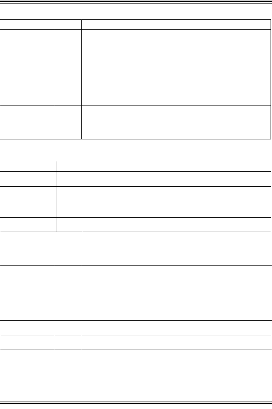
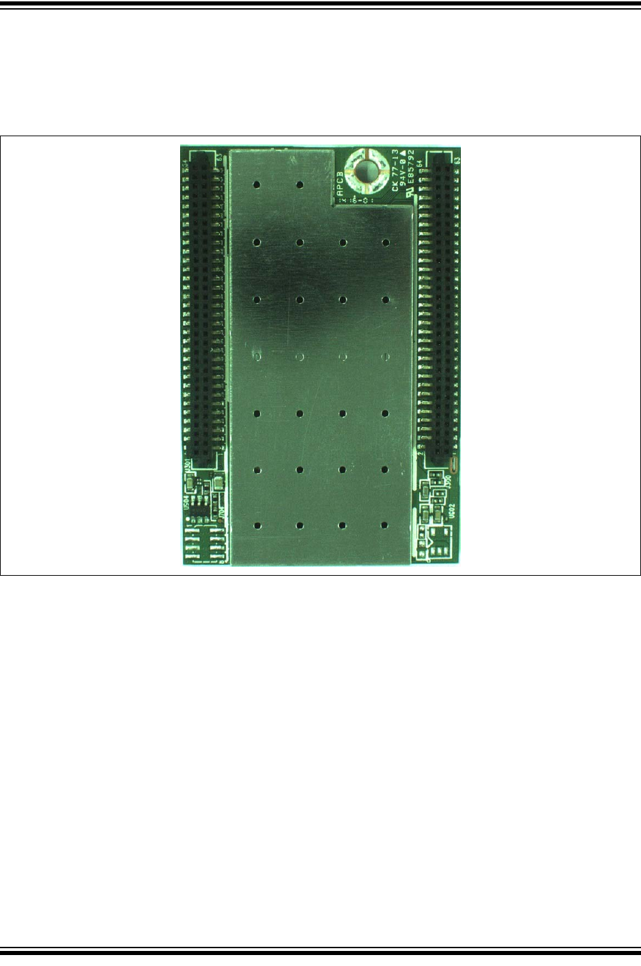
2.0 CY920 BOARD LAYOUT AND
FEATURES
This section describes the CY920 board and its key
components. All production modules include two RF
shields: the top shield and the bottom shield.
Figure 2-1
illustrates the top view of the CY920 board. The figure
does not show the RF
shields because the shields are
temporarily removed to indicate the components.
2.1 Top View of CY920 Board
The top view of the CY920 board features the following
key components:
1. DM920 SoC
2. DDR2 SDRAM
3. SPI Flash
4. Ethernet PHY
5. Wi-Fi Front-end
6. Bluetooth SoC
7. Wi-Fi/BT Antenna Socket
8. Wi-Fi Antenna Socket
FIGURE 2-1: CY920 BOARD (TOP VIEW)
Note: This data sheet summarizes the features
of the CY920 network media module. It is
not intended to be a comprehensive
reference source. To complement the
information in this data sheet, refer to the
various application notes available on the
Microchip web site www.microchip.com.
7
8
5
6
1
4
2
3
© 2014 Microchip Technology Inc. Preliminary DS60001270C-page 19
CY920
3.0 APPLICATION GUIDELINES
This section describes the power-up sequence and the
RF guidelines recommended by Microchip.
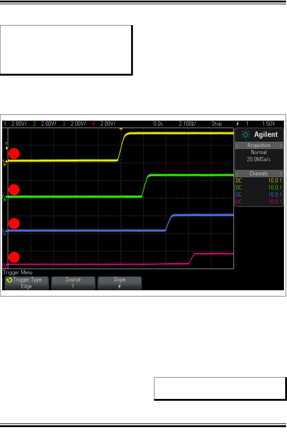
3.1 Power Sequencing and Reset
Timing
The power sequencing during power on should start
with the highest voltage rail. The power sequencing
should progress from the higher voltage rail to the
lower voltage rail, i.e power-up 3.3V, 2.5V, 1.8V, and
then 1.2V with a delay of 2 ms between each power rail.
During power-down, the power sequencing should be
in the reverse direction, i.e., remove 1.2V, 1.8V, 2.5V,
and then 3.3V. The power-up sequence is mandatory
and the power-down sequence is preferred, but
optional. Figure 3-1 illustrates the power-up timing.
FIGURE 3-1: POWER-UP SEQUENCE
3.2 RF Considerations
The overall performance of the system, RF, and
Wi-Fi/BT is significantly affected by the product design,
environment and application. It is the responsibility of
the product designer to ensure system level shielding
(if required) and to verify the performance of the given
product features and applications.
The Wi-Fi/BT performance will be affected by the RF
environment surrounding the CY920 module. Consider
the following precautions for optimal Wi-Fi/BT
performance:
• The CY920 module is positioned in a noise-free
RF environment, i.e, away from high frequency
clock signals and any other sources of RF energy.
• The antenna is not shielded by any metal objects,
such as loudspeakers or any other metal parts.
• The power supplies are clean and noise-free.
Note: This data sheet summarizes the features
of the CY920 network media module. It is
not intended to be a comprehensive
reference source. To complement the
information in this data sheet, refer to the
various application notes available on the
Microchip web site www.microchip.com.
3.3V
2.5V
1.8V
1.2V
Note: The CY920 module includes RF shielding
on the top and bottom of the board as a
standard feature.

CY920
DS60001270C-page 20 Preliminary © 2014 Microchip Technology Inc.
NOTES:

© 2014 Microchip Technology Inc. Preliminary DS60001270C-page 21
CY920
4.0 Wi-Fi SPECIFICATION
Table 4-1 describes the Wi-Fi specifications of the
CY920 module.
TABLE 4-1: Wi-Fi® SPECIFICATIONS (1, 2, 4, 5, 6)
Feature Description
WLAN Standards
IEEE 802.11a
IEEE 802.11b
IEEE 802.11g
IEEE 802.11n
Frequency
Band/Channels
2.412 - 2.472 GHz (2.4 GHz ISM Band, 13 Channels)
Channel 1 - Channel 13
5.180 - 5.240 GHz (U-NII lower band)
5.260 - 5.320 GHz (U-NII middle band), see Note 3
5.500 - 5.700 GHz (U-NII middle band extended), see Note 3
5.745 - 5.825 GHz (U-NII upper band/ISM band)
North America FCC, Japan Telec, Europe ETSI
Modulation
802.11a mode (OFDM: IEEE 802.11a)
802.11b mode (DS-SS: IEEE 802.11b)
802.11g mode (OFDM: IEEE 802.11g)
802.11n mode (OFDM: IEEE 802.11n)
Transmission Speed
802.11a mode
54 Mbps, 48 Mbps, 36 Mbps, 24 Mbps, 18 Mbps, 12 Mbps, 9 Mbps, 6 Mbps
802.11b mode
11 Mbps, 5.5 Mbps, 2 Mbps, 1 Mbps
802.11g mode
54 Mbps, 48 Mbps, 36 Mbps, 24 Mbps, 18 Mbps, 12 Mbps, 9 Mbps, 6 Mbps
802.11n mode
MCS0 to MCS7(20 MHz and 40 MHz supported)
Normal and short GI supported (PHY data rates up to 150 Mbps for 40 MHz mode + short GI)
Note 1: With respect to TX power, different (higher/lower) RF output power settings may be used for specific
regions, antennas and/or enclosures, in which case recertification may be required.
2: 802.11n Greenfield is not supported. (Greenfield forces 802.11n operation even in the presence of
802.11b/g AP)
3: Dynamic Frequency Selection (DFS) is supported by the hardware. Firmware support for DFS may not be
in initial firmware releases, but will follow in a later firmware release.
4: 802.11n 20 MHz and 40 MHz bandwidth is supported.
5: The availability of some specific channels and/or operational frequency bands are country dependent and
are firmware programmed at the Host product factory to match the intended destination. The firmware
setting is not accessible to the end user of the Host product.
6: Specifications are based on nominal test settings during module production at room temperature.

CY920
DS60001270C-page 22 Preliminary © 2014 Microchip Technology Inc.
TX Power
802.11a mode
+12.5 dBm +/-3 dB (U-NII lower and U-NII upper/ISM band)
802.11n HT20 mode
+11.5 dBm +/-3 dB (U-NII lower and U-NII upper/ISM band)
802.11n HT40 mode
+10 dBm +/-3 dB (U-NII lower and U-NII upper/ISM band)
802.11b mode
+16.5 dBm +/- 3 dB
802.11g mode
+13 dBm +/-3 dB
802.11n (HT20/40) mode
+12 dBm +/-3 dB (2.4GHz ISM)
Power-on Ramp Adhering to IEEE specification
RF Carrier
Suppression
Adhering to IEEE specification
TX EVM
802.11a mode
-25 dB at 54 Mbps
802.11b mode
-10 dB at 11 Mbps
802.11g mode
-25 dB at 54 Mbps
802.11n mode
-27 dB at MCS7
RX Sensitivity 802.11a mode
-65 dB at 54 Mbps
802.11b mode
-76 dB at 11 Mbps
802.11g mode
-65 dB at 54 Mbps
802.11n mode
-64 dB at MCS7/20 MHz; -61 dB at MCS7/40 MHz
Throughput rate
(measured for each
module)
See factory test specification
TABLE 4-1: Wi-Fi® SPECIFICATIONS (1, 2, 4, 5, 6) (CONTINUED)
Feature Description
Note 1: With respect to TX power, different (higher/lower) RF output power settings may be used for specific
regions, antennas and/or enclosures, in which case recertification may be required.
2: 802.11n Greenfield is not supported. (Greenfield forces 802.11n operation even in the presence of
802.11b/g AP)
3: Dynamic Frequency Selection (DFS) is supported by the hardware. Firmware support for DFS may not be
in initial firmware releases, but will follow in a later firmware release.
4: 802.11n 20 MHz and 40 MHz bandwidth is supported.
5: The availability of some specific channels and/or operational frequency bands are country dependent and
are firmware programmed at the Host product factory to match the intended destination. The firmware
setting is not accessible to the end user of the Host product.
6: Specifications are based on nominal test settings during module production at room temperature.
© 2014 Microchip Technology Inc. Preliminary DS60001270C-page 23
CY920
5.0 BLUETOOTH SPECIFICATIONS
The Bluetooth (BT) subsystem included in the CY920
module shares the antenna connections with the Wi-Fi
subsystem. Dedicated control signals between the
DM920 module and the BT controller perform Packet
Traffic Arbitration (PTA) to optimise co-existence
between the Wi-Fi and BT subsystems. A high-speed
UART interface is used to send data from the BT
controller to the DM920 SoC for further processing.
5.1 Features
The following are the Bluetooth features:
• Compliant with Bluetooth v2.1 + EDR
specification
• SBC and AAC codec
• A2DP and AVRCP profiles
• WLAN and Bluetooth co-existence using PTA and
AFH
• Utilises single antenna, shared with Wi-Fi
• Operating band: 2.4 GHz ISM band
• Output power Class 2 (+4 dBm)
• Low power consumption
5.2 Bluetooth Radio Characteristics
Table 5-1 provides Rx and Tx characteristics of the
Bluetooth radio.
TABLE 5-1: RADIO CHARACTERISTICS
Parameter Min. Typical Max. Bluetooth
Spec Units
Sensitivity at 0.1% BER — — — ≤ -70 dBm
RF transmit power -6 — 4 ≤ 4dBm
Initial carrier frequency tolerance — 25 75 75 kHz
20 dB bandwidth for modulated carrier — — 1000 ≤ 1000 kHz
Modulation characteristics (f1_ave) 140 165 175 > 140 kHz
Modulation characteristics (f2_max) 115 145 — ≥ 115 kHz
Note 1: Specifications are based on nominal test settings during module production at room temperature.

CY920
DS60001270C-page 24 Preliminary © 2014 Microchip Technology Inc.
NOTES:
© 2014 Microchip Technology Inc. Preliminary DS60001270C-page 25
CY920
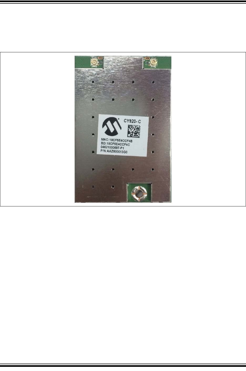
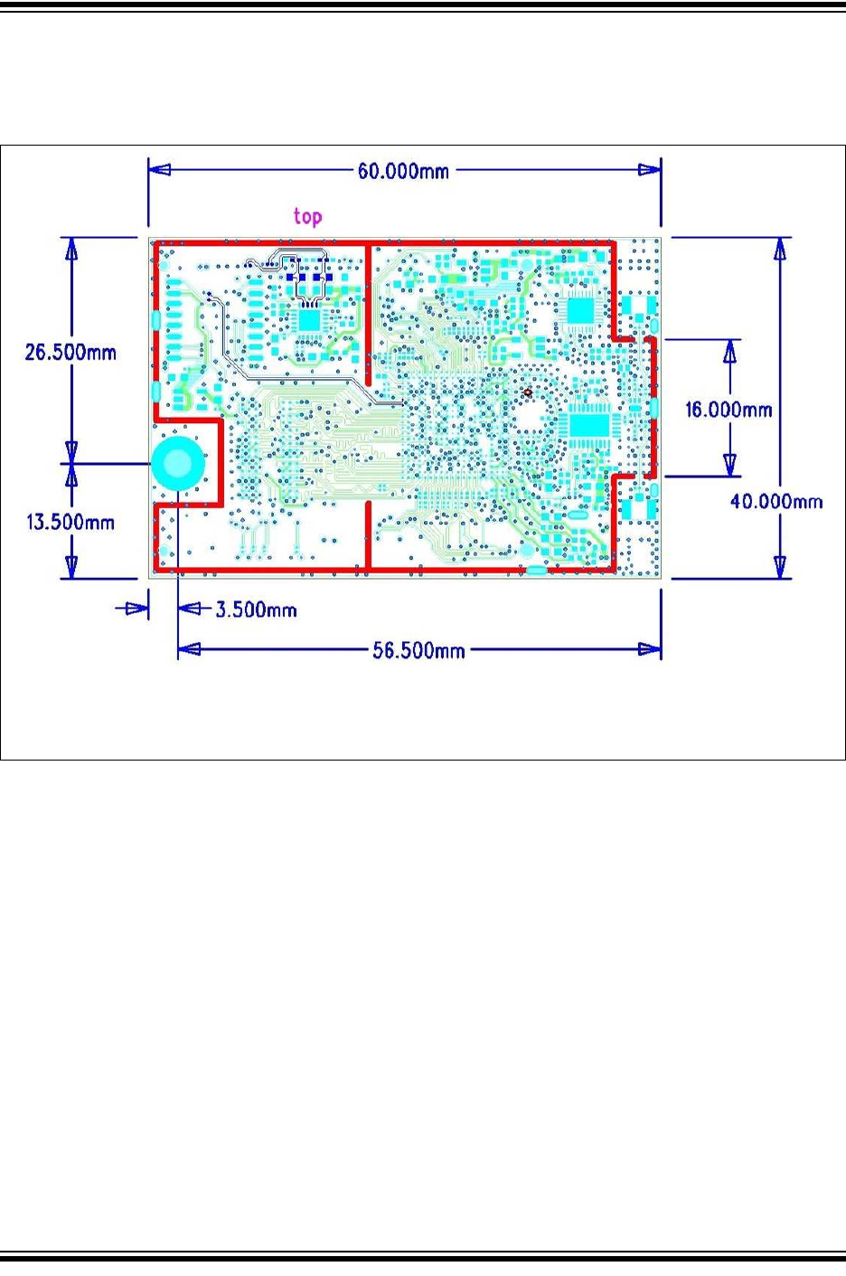
6.0 PACKAGING INFORMATION
Figure 6-1 and Figure 6-2 illustrate the top and bottom
dimensions of the CY920 board.
FIGURE 6-1: CY920 BOARD DIMENSIONS (TOP VIEW)
Note 1: PCB panel width and height tolerance is 0.1 mm.
2: Plated hole is 0.075 mm.
3: Non-plated hole is 0.05 mm.
CY920
DS60001270C-page 26 Preliminary © 2014 Microchip Technology Inc.
FIGURE 6-2: CY920 BOARD DIMENSIONS (BOTTOM VIEW)
Note 1: PCB panel width and height tolerance is 0.1 mm.
2: Plated hole is 0.075 mm.
3: Non-plated hole is 0.05 mm.

© 2014 Microchip Technology Inc. Preliminary DS60001270C-page 29
CY920
7.0 ELECTRICAL CHARACTERISTICS
This section provides an overview of the electrical characteristics of the CY920 module. Additional information will be
provided in future revisions of this document as it becomes available.
Absolute maximum ratings for the CY920 network media module are listed in the following table.
Absolute Maximum Ratings
Table 7-1 provides the basic electric specifications of the CY920 module.
TABLE 7-1: BASIC SPECIFICATIONS
Parameter Component Min. Max. Unit
3.3V Supply Voltage
Main
-0.5 4.6 V
1.2V Supply Voltage -0.5 1.8 V
1.8V Supply Voltage -0.5 2.1 V
2.5V Supply Voltage -0.5 3.0 V
†NOTICE: Stresses above those listed under “Absolute Maximum Ratings” may cause permanent damage to the
device. This is a stress rating only and functional operation of the device at those or any other conditions above
those indicated in the operation listings of this specification, is not implied. Exposure to maximum rating conditions
for extended periods may affect device reliability.
Parameter Symbol Min. Typ Max. Unit
Power supply input voltage VIN 3.165
1.14
1.71
2.375
3.3
1.2
1.8
2.5
3.465
1.26
1.89
2.625
V
V
V
V
Logic input high voltage VIH 2—3.6V
Logic input low voltage VIL -0.3 — 0.8 V
Logic input threshold voltage VT1.39 1.51 1.65 V
Schmitt-trigger input low to high threshold
voltage
VT+ 1.63 1.76 1.9 V
Schmitt-trigger input high to low threshold
voltage
VT- 1.18 1.3 1.44 V
Logic output high voltage VOH 2.4 — — V
Logic output low voltage VOL ——0.4V
Logic low-level output current
(VOL=0.4V)
IOL 10.0 15.2 20.2 mA
Logic high-level output current
(VOH=2.4V)
IOH 13.9 28.0 48.2 mA

CY920
DS60001270C-page 30 Preliminary © 2014 Microchip Technology Inc.
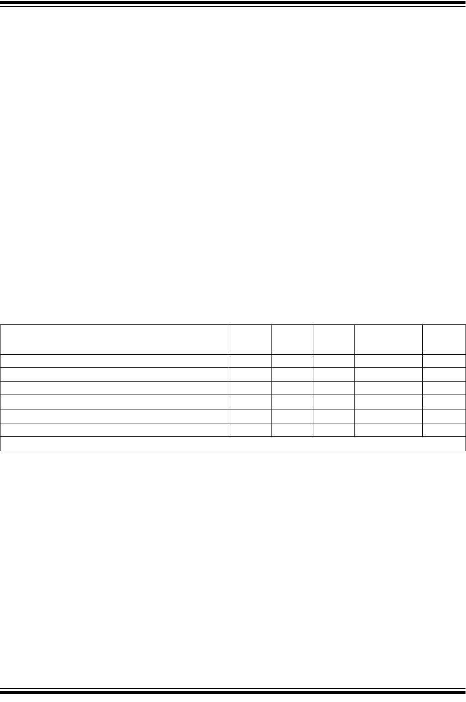
Table 7-2 provides the current consumption details in
various measurement conditions.
The current consumption per voltage rail and power
consumption details will be provided in the future
revision of this document.
TABLE 7-2: POWER CONSUMPTION(1)
Measurement Condition
Current Consumption per
Voltage Rail (mA) Power
Consumption
(mW)
1.2V 1.8V 2.5V 3.3V
Maximum expected current consumption per rail across operating
modes (continuous Tx/Rx mode with all function active), see
Note 2.
———— —
Wi-Fi streaming (Ethernet, USB and Bluetooth power-down) — — — — —
Wi-Fi streaming (USB active, Ethernet and Bluetooth power-down) — — — — —
Wi-Fi streaming (USB and Bluetooth active) — — — — —
Ethernet streaming (Wi-Fi, USB and Bluetooth power-down) — — — — —
Ethernet streaming (USB active, Wi-Fi and Bluetooth power-down) — — — — —
Bluetooth streaming (Ethernet, Wi-Fi and USB power down) — — — — —
Bluetooth streaming (USB active, Ethernet and Wi-Fi power-down) — — — — —
Bluetooth streaming (Ethernet active, Wi-Fi and USB power down) — — — — —
PSM wake up on Wi-Fi (PSM JB Green) (DTIM=1), see Note 2———— —
PSM wake up on Wi-Fi (PSM JB Green) (DTIM=1), see Note 2———— —
PSM wake up on Ethernet and wake on Wi-Fi (PSM JB Green) — — — — —
Hibernate mode: Wake on Host or GPIO (Wi-Fi, Ethernet,
Bluetooth and USB in power-down), see Note 2———— —
Hibernate mode: Wake on Host or GPIO (Wi-Fi, Ethernet,
Bluetooth and USB in power-down), see Note 2———— —
CY920 module held in Reset — — — — —
Note 1: All current consumptions are estimates, and will be revised after initial modules are characterised.
2: The worst case maximum is when all functions are active and when the Wi-Fi is transmitting in continuous
Tx/Rx mode. This mode is used only during the Wi-Fi RF certification test. A separate software will be
required to perform this test. Power supplies should be designed with some additional derating on top of
the maximum value, typically +30%.

© 2014 Microchip Technology Inc. Preliminary DS60001270C-page 31
CY920
Table 7-3 lists the CY920 module operating conditions.
TABLE 7-3: OPERATING CONDITIONS
Parameter Min. Max. Unit
Operating Temperature 0 +70 °C
Operating Humidity 10 90 (non-condensing) %RH
Storage Temperature -10 +75 °C
Storage Humidity 10 95 (non-condensing) %RH
Storage Temperature Cycle Test (24 hrs) -10 +75 °C
Note 1: For more information on various SKUs of the CY920 module, refer to Tab l e 9 - 1 .

CY920
DS60001270C-page 32 Preliminary © 2014 Microchip Technology Inc.
NOTES:
© 2014 Microchip Technology Inc. Preliminary DS60001270C-page 33
CY920
8.0 REGULATORY COMPLIANCE
AND QUALITY
This section addresses the various regulatory
standards that are compliant with the CY920 module.
Microchip does not certify all module variants for all the
countries. Ta b le 8 - 1 provides the module versions for
which certain certifications have already been done.
The information about certified modules and Bluetooth
qualifications will be provided in the future revisions of
this document.
TABLE 8-1: REGULATORY COMPLIANCE
Contact Microchip’s sales office for the latest
information on certified modules for a particular county,
and arranging for an additional certification for your
chosen module, if needed. Any additional certification
will need to be paid for by the customer.
The product manufacturer is responsible for the end
product certification. Microchip can help manufacturers
to prepare for the Wi-Fi
Alliance test for the Wi-Fi
certification by providing an example test plan and the
required commands to enable special test modes.
Please contact Microchip’s sales office for any
assistance on Wi-Fi Alliance Logo certification.
For documents related to Wi-Fi certification and
recommended interfacing and power supply
schematics, refer to the Microchip web site at
www.microchip.com.
.
Note: This data sheet summarizes the features
of the CY920 network media module. It is
not intended to be a comprehensive
reference source. To complement the
information in this data sheet, refer to the
various application notes available on the
Microchip web site www.microchip.com.
Description Country Compliance Certified Modules
Electromagnetic Compatibility
(Prescan)
USA FCC CFR47 Part15B
—
Europe EN 301 489-1
EN 301 489-17
Canada IC RSS-GEN
Radio Regulations
USA FCC CFR47 Part 15C, para 15.247
FCC CFR47 Part 15E, para 15.407
—
Europe EN 300 328
EN 301 893
Canada IC RSS-210
Japan ARIB STD-T66
ARIB STD-T71
Bluetooth Qualifications — — —
CY920
DS60001270C-page 34 Preliminary © 2014 Microchip Technology Inc.
8.1 Antenna Considerations
Table 8.2 provides the list of antennas along with the
manufacturer and part number details.
TABLE 8-2: ANTENNA LIST
Table 8.3 provides the antennas to be used for the
various SKUs as per Table 8.2.
TABLE 8-3: ANTENNAS FOR VARIOUS
SKUs
8.2 CY920 Usage Guidelines under
Modular Approval
The CY module has received Limited Module
Approval (LMA) from FCC and IC. This is because the
CY module does not have complete built-in Power
regulator circuit. Microchip recommends that
customers follow the supply voltage requirements
provided in this data sheet, and follow the Power
supply design provided in the “CY Module Power
Supply V1.0” document. It is the product manufacturer
responsibility to ensure that the power supply
recommendations are followed, and the RF behavior
adheres the FCC or TCB certification requirements
when the module is installed in the final Host product.
The product manufacturer should work with their test
house for confirming the RF behavior with FCC or TCB.
8.3 Restriction of Use of Hazardous
Substances (RoHS) Compliance
CY920 module uses only RoHS compliant components.
Sl No. Manufacturer Part Number Antenna Type Peak Gain
1 WALSIN PI_RFDPA870920IMLB301_V01 Dipole Antenna 1.84 dBi for 2.4 GHz
2 WALSIN PI_RFDPA870920IMLB301_V01 Dipole Antenna 3.26 dBi for 5 GHz
3 WALSIN PI_RFDPA870930IMLB301_V01 Dipole Antenna 1.10 dBi for 2.4 GHz
4 WALSIN PI_RFDPA870930IMLB301_V01 Dipole Antenna 2.77 dBi for 5 GHz
5 WALSIN RFDPA870930IMAB301 Dipole Antenna 1.2 dBi for 2.4 GHz
6 WALSIN RFDPA870945IMAB301 Dipole Antenna 1.16 dBi for 2.4 GHz
7 WALSIN RFDPA870900SBAB801* +
RFCBA100630SA6B301
Dipole Antenna 0.7 dBi for 2.4 GHz
8 WALSIN RFDPA870900SBAB801* +
RFCBA100645SA6B301
Dipole Antenna 0.1 dBi for 2.4 GHz
Note 1: * The antenna connector is reverse SMA type.
Configuration Code Antenna List (Sl No.)
CY920-A 1, 2, 3, 4, 5, 6, 7, 8
CY920-B —
CY920-C 1, 2, 3, 4, 5, 6, 7, 8
Note 1: The antenna list for CY920-B SKU will be
provided in the future revisions of this
document.
CY920
DS60001270C-page 35 Preliminary © 2014 Microchip Technology Inc.
9.0 ORDERING GUIDE
Table 9-1 describes the various SKUs of CY920 network media module.
TABLE 9-1: ORDERING GUIDE(1)
Note: This data sheet summarizes the features of the CY920 network
media module. It is not intended to be a comprehensive reference
source. To complement the information in this data sheet, refer to
the various application notes available on the Microchip web site
www.microchip.com.
Part
number Microchip
IC Status Two External
Diversity
Antennas
Ethernet
(10/100 Mbps) USB Extended
Connector 64 MB
DDR2
16 MB
Serial
Flash Bluetooth Top Module
Shield Bottom
Module
Shield
CY920-A DM920 Launch 9—9—999 99
CY920-B DM920 Launch 9999 99—99
CY920-C DM920 Launch 9999999 99
Note 1: The Apple Authentication Coprocessor is not available on the CY920 module. The Apple Authentication Coprocessor should be provided on the product
motherboard, connected to the SDA, SCL signals from the CY920 module.
Note:
Do not use a module which has two external antenna connectors
with only one external antenna connected. Leaving one antenna
socket open will degrade Wi-Fi performance. Microchip
recommends using two external antennas for best performance.

CY920
DS60001270C-page 36 Preliminary © 2014 Microchip Technology Inc.
NOTES:

© 2014 Microchip Technology Inc. Preliminary DS60001270C-page 37
CY920
APPENDIX A: CERTIFICATION
NOTICES
The CY920 module is not tested for Federal
Communications Commission (FCC). The following
statements are not valid until the production version
modules are tested. It is planned to certify the
production version of the CY920 module as soon as
possible after production versions are made.
Federal Communications Commission
Interference Statement
This equipment has been tested and found to comply
with the limits for a Class B digital device, pursuant to
part 15 of the FCC Rules. These limits are designed to
provide reasonable protection against harmful
interference in a residential installation. This equipment
generates, uses, and radiates radio frequency energy
and, if not installed and used in accordance with the
instructions, may cause harmful interference to radio
communications. However, there is no guarantee that
interference will not occur in a particular installation. If
this equipment does cause harmful interference to
radio or television reception, which can be determined
by turning the equipment off and on, the user is
encouraged to try to correct the interference by one or
more of the following measures:
• Reorient or relocate the receiving antenna.
• Increase the separation between the equipment
and receiver.
• Connect the equipment into an outlet on a circuit
different from that to which the receiver is
connected.
• Consult the dealer or an experienced radio/ TV
technician for help.
Labeling Requirements
This device complies with Part 15 of the FCC Rules. The
operation is subject to the following two conditions: the
device may not cause harmful interference, and the
device must accept any interference received, including
interferences that may cause undesired operations.
RF Exposure Warning
This equipment must be installed and operated in
accordance with provided instructions. The antennas
used for this transmitter must be installed to provide a
separation distance of at least 20 cm from all persons
and must not be co-located or operating in conjunction
with any other antenna or transmitter. End users and
installers must be provide with antenna installation
instructions and transmitter operating
conditions for satisfying RF exposure compliance.
Information for the OEMs or Integrators
The following statement must be included in all
versions of this document supplied to OEMs or
integrators, but should not be distributed to the end
user.
“This device is intended for OEM or integrators only.
Please see the full Grant of Equipment document for
other restrictions. This device must be operated and
used with a locally approved Access “.
Information to be Supplied to the End
User by the OEM or Integrator
The following regulatory and safety notices must be
published in all documentation supplied to the end user
of the product or system, incorporating an adapter in
compliance with local regulations.
“The host system must be labelled with: Contains FCC
ID:ZQO-CY920‘X’ and IC: 2581A-CY920‘X’, FCC ID
displayed on the label.
The letter shown in Ordering Guide Part Number
column should be substituted for ‘X’. For example, for
the CY920-C module, the label text should be
"Contains FCC ID:ZQO-CY920C"and "IC:
2581A-CY920C. The label text should be updated
according to the table shown in Section 9.0 “Ordering
Guide” of this document.
Caution:Any changes or modifications not
expressly approved by the grantee of this
device could void the user's authority to
operate the equipment.
Applicable to UNII device only:
The
device is restricted to indoor use when
operating in the 5.15 GHz to 5.25 GHz
frequency band. FCC requires this
product to be used indoors for frequency
range 5.15 GHz to 5.25 GHz to reduce
the potential for harmful interference to
co-channel mobile satellite systems.

CY920
DS60001270C-page 38 Preliminary © 2014 Microchip Technology Inc.
Japan
This device operation in the 5.15 GHz to 5.35 GHz
frequency range is restricted to indoor use. Final
product shall be labelled "For Indoor use only."
Canada, Industry Canada (IC) Notices
This Class B digital apparatus complies with Canadian
ICES-003 and RSS-210.
Operation is subject to the following two conditions: the
device may not cause interference, and the device
must accept any interference, including interference
that may cause undesired operation of the device.
This radio transmitter "IC: 2581A-CY920‘X’ has been
approved by Industry Canada to operate with the
antenna types listed in Table 8.2 with the maximum
permissible gain and required antenna impedance for
each antenna type indicated. Antenna types not
included in this list, having a gain greater than the
maximum gain indicated for that type, are strictly
prohibited for use with this device.
RF Exposure Information
The radiated output power of the wireless device is
below the Industry Canada (IC) radio frequency
exposure limits. The Wireless Device should be used in
such a manner that the potential for human contact
during normal operation is minimized.
This device has been evaluated and shown compliant
with the IC radio frequency exposure limits under
mobile exposure conditions. (antennas are greater
than 20cm from a person's body).
This device has been certified for use in Canada.
Status of the listing in the Industry Canada's Radio
Equipment List (REL) can be found at the following
locations:
http://www.ic.gc.ca/app/sitt/reltel/srch/nwRdSrch.do?la
ng=eng
Additional Canadian information on RF exposure can
be found at the following location:
http://www.ic.gc.ca/eic/site/smt-gst.nsf/eng/sf08792.ht
ml
Canada, avis d'Industry Canada (IC)
Cet appareil numérique de classe B est conforme aux
normes canadiennes ICES-003 et RSS-210.
Son fonctionnement est soumis aux deux conditions
suivantes: (1) cet appareil ne doit pas causer
d'interférence et (2) cet appareil doit accepter toute
interférence, notamment les interférences qui peuvent
affecter son fonctionnement.
Cet émetteur radio "IC: 2581A-CY920‘X’ a été
approuvé par Industrie Canada pour fonctionner avec
les types d'antennes énumérés dans le tableau 7-2
avec le gain maximal admissible et impédance
d'antenne requise pour chaque type d'antenne indiqué.
Types d'antennes n'est pas inclus dans cette liste,
ayant un gain supérieur au gain maximal indiqué pour
ce type, sont strictement interdits pour une utilisation
avec cet appareil.
Informations concernant l'exposition aux
fréquences radio (RF)
La puissance de sortie émise par l'appareil de sans fil
Dell est inférieure à la limite d'exposition aux
fréquences radio d'Industry Canada (IC). Utilisez
l'appareil de sans fil Dell de façon à minimiser les
contacts humains lors du fonctionnement normal.
Ce périphérique a également été évalué et démontré
conforme aux limites d'exposition aux RF d'IC dans des
conditions d'exposition à des appareils mobiles (les
antennes se situent à moins de 20 cm du corps d'une
personne).
Ce périphérique est homologué pour l'utilisation au
Canada. Pour consulter l'entrée correspondant à
l'appareil dans la liste d'équipement radio (REL - Radio
Equipment List) d'Industry Canada rendez-vous sur:
http://www.ic.gc.ca/app/sitt/reltel/srch/nwRdSrch.do?la
ng=eng
Pour des informations supplémentaires concernant
l'exposition aux RF au Canada rendez-vous sur:
http://www.ic.gc.ca/eic/site/smt-gst.nsf/eng/sf08792.ht
ml
Caution:Applicable to LE-LAN device only: This
device is restricted to indoor use when
operating in the 5.15 GHz to 5.25 GHz
frequency band. Industry Canada
requires this product to be used indoors
for frequency range 5.15 to 5.25 GHz to
reduce the potential for harmful
interference to co-channel Mobile Satellite
systems.
Caution:Prudence (ce n'est applicable qu'aux
dispositif LE-LAN): Ce dispositif est limité
à une utilisation en intérieur à cause de
son fonctionnement dans la gamme 5.15
GHz à 5.25 GHz. Industrie Canada exige
que ce produit est utilisé à l'intérieur pour
la gamme de fréquence de 5,15 à 5,25
GHz pour réduire les risques
d'interférence nuisible à la co-canal
systèmes mobiles par satellite.

© 2014 Microchip Technology Inc. Preliminary DS60001270C-page 39
CY920
APPENDIX B: REVISION HISTORY
Revision A (January 2014)
This is the initial release of the CY920 Network Media
Module data sheet.
Revision B (March 2014)
•Replaced Figure 6-1 and Figure 6-2 in
Section 6.0 “Packaging Information”
• Added Figure 2-3 and Figure 2-4
Revision C (June 2014)
This revision includes the following updates:
• Figures:
- Updated Figure 2-1, Figure 2-2, Figure 2-3,
and Figure 2-4
- Added Figure 3-1
-Replaced Figure 6-1 and Figure 6-2
• Notes:
- Updated Note 4 in Table 4-1
- Added Note 6 in Table 4-1
- Removed Note 3 in Ta b l e 7 - 2
• Sections:
- Updated the components in Section 2.1
“Top View of CY920 Board”
- Updated Section 3.1 “Power Sequencing
and Reset Timing”
- Updated Section 8.2 “CY920 Usage
Guidelines under Modular Approval”
• Tables:
- Updated Table 1-1, Tab l e 4 - 1 , and Table 7-2
-Replaced Table 5 - 1 and Ta bl e 8 - 2
- Removed Table 5-2
- Added Ta b l e 6 - 1 and Table 8-3
- Removed the CY920-E SKU in Table 9 - 1
• Minor changes related to formatting have been
incorporated in the entire document

CY920
DS60001270C-page 40 Preliminary © 2014 Microchip Technology Inc.
NOTES:

© 2014 Microchip Technology Inc. Preliminary DS60001270C-page 41
CY920
THE MICROCHIP WEB SITE
Microchip provides online support via our WWW site at
www.microchip.com. This web site is used as a means
to make files and information easily available to
customers. Accessible by using your favorite Internet
browser, the web site contains the following
information:
•Product Support – Data sheets and errata,
application notes and sample programs, design
resources, user’s guides and hardware support
documents, latest software releases and archived
software
•General Technical Support – Frequently Asked
Questions (FAQ), technical support requests,
online discussion groups, Microchip consultant
program member listing
•Business of Microchip – Product selector and
ordering guides, latest Microchip press releases,
listing of seminars and events, listings of
Microchip sales offices, distributors and factory
representatives
CUSTOMER CHANGE NOTIFICATION
SERVICE
Microchip’s customer notification service helps keep
customers current on Microchip products. Subscribers
will receive e-mail notification whenever there are
changes, updates, revisions or errata related to a
specified product family or development tool of interest.
To register, access the Microchip web site at
www.microchip.com. Under “Support”, click on
“Customer Change Notification” and follow the
registration instructions.
CUSTOMER SUPPORT
Users of Microchip products can receive assistance
through several channels:
• Distributor or Representative
• Local Sales Office
• Field Application Engineer (FAE)
• Technical Support
Customers should contact their distributor,
representative or Field Application Engineer (FAE) for
support. Local sales offices are also available to help
customers. A listing of sales offices and locations is
included in the back of this document.
Technical support is available through the web site
at: http://microchip.com/support

CY920
DS60001270C-page 42 Preliminary © 2014 Microchip Technology Inc.
NOTES:

DS60001270C-page 43 © 2014 Microchip Technology Inc.
AMERICAS
Corporate Office
2355 West Chandler Blvd.
Chandler, AZ 85224-6199
Tel: 480-792-7200
Fax: 480-792-7277
Technical Support:
http://www.microchip.com/
support
Web Address:
www.microchip.com
Atlanta
Duluth, GA
Tel: 678-957-9614
Fax: 678-957-1455
Austin, TX
Tel: 512-257-3370
Boston
Westborough, MA
Tel: 774-760-0087
Fax: 774-760-0088
Chicago
Itasca, IL
Tel: 630-285-0071
Fax: 630-285-0075
Cleveland
Independence, OH
Tel: 216-447-0464
Fax: 216-447-0643
Dallas
Addison, TX
Tel: 972-818-7423
Fax: 972-818-2924
Detroit
Novi, MI
Tel: 248-848-4000
Houston, TX
Tel: 281-894-5983
Indianapolis
Noblesville, IN
Tel: 317-773-8323
Fax: 317-773-5453
Los Angeles
Mission Viejo, CA
Tel: 949-462-9523
Fax: 949-462-9608
New York, NY
Tel: 631-435-6000
San Jose, CA
Tel: 408-735-9110
Canada - Toronto
Tel: 905-673-0699
Fax: 905-673-6509
ASIA/PACIFIC
Asia Pacific Office
Suites 3707-14, 37th Floor
Tower 6, The Gateway
Harbour City, Kowloon
Hong Kong
Tel: 852-2943-5100
Fax: 852-2401-3431
Australia - Sydney
Tel: 61-2-9868-6733
Fax: 61-2-9868-6755
China - Beijing
Tel: 86-10-8569-7000
Fax: 86-10-8528-2104
China - Chengdu
Tel: 86-28-8665-5511
Fax: 86-28-8665-7889
China - Chongqing
Tel: 86-23-8980-9588
Fax: 86-23-8980-9500
China - Hangzhou
Tel: 86-571-8792-8115
Fax: 86-571-8792-8116
China - Hong Kong SAR
Tel: 852-2943-5100
Fax: 852-2401-3431
China - Nanjing
Tel: 86-25-8473-2460
Fax: 86-25-8473-2470
China - Qingdao
Tel: 86-532-8502-7355
Fax: 86-532-8502-7205
China - Shanghai
Tel: 86-21-5407-5533
Fax: 86-21-5407-5066
China - Shenyang
Tel: 86-24-2334-2829
Fax: 86-24-2334-2393
China - Shenzhen
Tel: 86-755-8864-2200
Fax: 86-755-8203-1760
China - Wuhan
Tel: 86-27-5980-5300
Fax: 86-27-5980-5118
China - Xian
Tel: 86-29-8833-7252
Fax: 86-29-8833-7256
China - Xiamen
Tel: 86-592-2388138
Fax: 86-592-2388130
China - Zhuhai
Tel: 86-756-3210040
Fax: 86-756-3210049
ASIA/PACIFIC
India - Bangalore
Tel: 91-80-3090-4444
Fax: 91-80-3090-4123
India - New Delhi
Tel: 91-11-4160-8631
Fax: 91-11-4160-8632
India - Pune
Tel: 91-20-3019-1500
Japan - Osaka
Tel: 81-6-6152-7160
Fax: 81-6-6152-9310
Japan - Tokyo
Tel: 81-3-6880- 3770
Fax: 81-3-6880-3771
Korea - Daegu
Tel: 82-53-744-4301
Fax: 82-53-744-4302
Korea - Seoul
Tel: 82-2-554-7200
Fax: 82-2-558-5932 or
82-2-558-5934
Malaysia - Kuala Lumpur
Tel: 60-3-6201-9857
Fax: 60-3-6201-9859
Malaysia - Penang
Tel: 60-4-227-8870
Fax: 60-4-227-4068
Philippines - Manila
Tel: 63-2-634-9065
Fax: 63-2-634-9069
Singapore
Tel: 65-6334-8870
Fax: 65-6334-8850
Taiwan - Hsin Chu
Tel: 886-3-5778-366
Fax: 886-3-5770-955
Taiwan - Kaohsiung
Tel: 886-7-213-7830
Taiwan - Taipei
Tel: 886-2-2508-8600
Fax: 886-2-2508-0102
Thailand - Bangkok
Tel: 66-2-694-1351
Fax: 66-2-694-1350
EUROPE
Austria - Wels
Tel: 43-7242-2244-39
Fax: 43-7242-2244-393
Denmark - Copenhagen
Tel: 45-4450-2828
Fax: 45-4485-2829
France - Paris
Tel: 33-1-69-53-63-20
Fax: 33-1-69-30-90-79
Germany - Dusseldorf
Tel: 49-2129-3766400
Germany - Munich
Tel: 49-89-627-144-0
Fax: 49-89-627-144-44
Germany - Pforzheim
Tel: 49-7231-424750
Italy - Milan
Tel: 39-0331-742611
Fax: 39-0331-466781
Italy - Venice
Tel: 39-049-7625286
Netherlands - Drunen
Tel: 31-416-690399
Fax: 31-416-690340
Poland - Warsaw
Tel: 48-22-3325737
Spain - Madrid
Tel: 34-91-708-08-90
Fax: 34-91-708-08-91
Sweden - Stockholm
Tel: 46-8-5090-4654
UK - Wokingham
Tel: 44-118-921-5800
Fax: 44-118-921-5820
Worldwide Sales and Service
03/25/14

© 2014 Microchip Technology Inc. DS60001270C-page 44
Information contained in this publication regarding device
applications and the like is provided only for your convenience
and may be superseded by updates. It is your responsibility to
ensure that your application meets with your specifications.
MICROCHIP MAKES NO REPRESENTATIONS OR
WARRANTIES OF ANY KIND WHETHER EXPRESS OR
IMPLIED, WRITTEN OR ORAL, STATUTORY OR
OTHERWISE, RELATED TO THE INFORMATION,
INCLUDING BUT NOT LIMITED TO ITS CONDITION,
QUALITY, PERFORMANCE, MERCHANTABILITY OR
FITNESS FOR PURPOSE. Microchip disclaims all liability
arising from this information and its use. Use of Microchip
devices in life support and/or safety applications is entirely at
the buyer’s risk, and the buyer agrees to defend, indemnify and
hold harmless Microchip from any and all damages, claims,
suits, or expenses resulting from such use. No licenses are
conveyed, implicitly or otherwise, under any Microchip
intellectual property rights.
Trademarks
The Microchip name and logo, the Microchip logo, dsPIC,
FlashFlex, flexPWR, JukeBlox, KEELOQ, KEELOQ logo, Kleer,
LANCheck, MediaLB, MOST, MOST logo, MPLAB,
OptoLyzer, PIC, PICSTART, PIC32 logo, RightTouch, SpyNIC,
SST, SST Logo, SuperFlash and UNI/O are registered
trademarks of Microchip Technology Incorporated in the
U.S.A. and other countries.
The Embedded Control Solutions Company and mTouch are
registered trademarks of Microchip Technology Incorporated
in the U.S.A.
Analog-for-the-Digital Age, BodyCom, chipKIT, chipKIT logo,
CodeGuard, dsPICDEM, dsPICDEM.net, ECAN, In-Circuit
Serial Programming, ICSP, Inter-Chip Connectivity, KleerNet,
KleerNet logo, MiWi, MPASM, MPF, MPLAB Certified logo,
MPLIB, MPLINK, MultiTRAK, NetDetach, Omniscient Code
Generation, PICDEM, PICDEM.net, PICkit, PICtail,
RightTouch logo, REAL ICE, SQI, Serial Quad I/O, Total
Endurance, TSHARC, USBCheck, VariSense, ViewSpan,
WiperLock, Wireless DNA, and ZENA are trademarks of
Microchip Technology Incorporated in the U.S.A. and other
countries.
SQTP is a service mark of Microchip Technology Incorporated
in the U.S.A.
Silicon Storage Technology is a registered trademark of
Microchip Technology Inc. in other countries.
GestIC is a registered trademarks of Microchip Technology
Germany II GmbH & Co. KG, a subsidiary of Microchip
Technology Inc., in other countries.
All other trademarks mentioned herein are property of their
respective companies.
© 2014, Microchip Technology Incorporated, Printed in the
U.S.A., All Rights Reserved.
ISBN: 978-1-63276-344-0
Note the following details of the code protection feature on Microchip devices:
• Microchip products meet the specification contained in their particular Microchip Data Sheet.
• Microchip believes that its family of products is one of the most secure families of its kind on the market today, when used in the
intended manner and under normal conditions.
• There are dishonest and possibly illegal methods used to breach the code protection feature. All of these methods, to our
knowledge, require using the Microchip products in a manner outside the operating specifications contained in Microchip’s Data
Sheets. Most likely, the person doing so is engaged in theft of intellectual property.
• Microchip is willing to work with the customer who is concerned about the integrity of their code.
• Neither Microchip nor any other semiconductor manufacturer can guarantee the security of their code. Code protection does not
mean that we are guaranteeing the product as “unbreakable.”
Code protection is constantly evolving. We at Microchip are committed to continuously improving the code protection features of our
products. Attempts to break Microchip’s code protection feature may be a violation of the Digital Millennium Copyright Act. If such acts
allow unauthorized access to your software or other copyrighted work, you may have a right to sue for relief under that Act.
Microchip received ISO/TS-16949:2009 certification for its worldwide
headquarters, design and wafer fabrication facilities in Chandler and
Tempe, Arizona; Gresham, Oregon and design centers in California
and India. The Company’s quality system processes and procedures
are for its PIC® MCUs and dsPIC® DSCs, KEELOQ® code hopping
devices, Serial EEPROMs, microperipherals, nonvolatile memory and
analog products. In addition, Microchip’s quality system for the design
and manufacture of development systems is ISO 9001:2000 certified.
QUALITYMANAGEMENTS
YSTEM
CERTIFIEDBYDNV
== ISO/TS16949==