MICROCHIP TECHNOLOGY RN2903 RN2903 Module User Manual RN2903
Microchip Technology Inc. RN2903 Module RN2903
Contents
- 1. User Manual
- 2. Users Manual
User Manual
2015 Microchip Technology Inc. Advance Information DS00000A-page 1
RN2903
General Features
• On-board LoRaWAN™ Class A protocol stack
• ASCII command interface over UART
• Compact form factor: 17.8 x 26.7 x 3 mm
• Castellated SMT pads for easy and reliable PCB
mounting
• Environmentally friendly, RoHS compliant
• Compliance:
- Modular Certified for the United States (FCC)
and Canada (IC)
- Australia and New Zealand
• Device Firmware Upgrade (DFU) over UART (see
“RN2903 LoRa™ Technology Module Command
Reference User’s Guide” DS40000000A)
Operational
• Single operating voltage: 2.1V to 3.6V (3.3V
typical)
• Temperature range: -40°C to +85°C
• Low-power consumption
• Programmable RF Communication Bit Rate up to
300 kbps with FSK modulation, 12500 bps with
LoRa™ Technology modulation
• Integrated MCU, Crystal, EUI-64 Node Identity
Serial EEPROM, Radio Transceiver with Analog
Front End, Matching Circuitry
• 14 GPIOs for control and status
RF/Analog Features
• Low-Power Long Range Transceiver operating in
the 915 MHz frequency band
• High Receiver Sensitivity: down to -148 dBm
• TX Power: adjustable up to +20 dBm high
efficiency PA
• FSK, GFSK, and LoRa Technology modulation
• IIP3 = -11 dBm
• >15 km coverage at suburban and >5 km
coverage at urban area
Description
Microchip’s RN2903 Low-Power Long Range LoRa
Technology Transceiver module provides an easy to
use, low-power solution for long range wireless data
transmission. The advanced command interface offers
rapid time to market.
The RN2903 module complies with the LoRaWAN
Class A protocol specifications. It integrates RF, a
baseband controller, command Application
Programming Interface (API) processor, making it a
complete long range solution.
The RN2903 module is suitable for simple long range
sensor applications with external host MCU.
Applications
• Automated Meter Reading
• Home and Building Automation
• Wireless Alarm and Security Systems
• Industrial Monitoring and Control
• Machine to Machine
• Internet of Things (IoT)
Low-Power Long Range LoRa™ Technology
Transceiver Module

RN2903
DS00000A-page 2 Advance Information 2015 Microchip Technology Inc.
Table of Contents
1.0 Device Overview .......................................................................................................................................................................... 3
2.0 General Specifications.................................................................................................................................................................. 6
3.0 Typical Hardware Connections..................................................................................................................................................... 8
4.0 Physical Dimensions .................................................................................................................................................................... 9
5.0 Application Information............................................................................................................................................................... 10
6.0 Regulatory Approval................................................................................................................................................................... 12
Appendix A: Revision History............................................................................................................................................................... 17
The Microchip Web Site....................................................................................................................................................................... 19
Customer Change Notification Service ................................................................................................................................................ 19
Customer Support................................................................................................................................................................................ 19
Product Identification System............................................................................................................................................................... 21
TO OUR VALUED CUSTOMERS
It is our intention to provide our valued customers with the best documentation possible to ensure successful use of your Microchip
products. To this end, we will continue to improve our publications to better suit your needs. Our publications will be refined and
enhanced as new volumes and updates are introduced.
If you have any questions or comments regarding this publication, please contact the Marketing Communications Department via
E-mail at docerrors@microchip.com. We welcome your feedback.
Most Current Data Sheet
To obtain the most up-to-date version of this data sheet, please register at our Worldwide Web site at:
http://www.microchip.com
You can determine the version of a data sheet by examining its literature number found on the bottom outside corner of any page.
The last character of the literature number is the version number, (e.g., DS30000000A is version A of document DS30000000).
Errata
An errata sheet, describing minor operational differences from the data sheet and recommended workarounds, may exist for current
devices. As device/documentation issues become known to us, we will publish an errata sheet. The errata will specify the revision
of silicon and revision of document to which it applies.
To determine if an errata sheet exists for a particular device, please check with one of the following:
• Microchip’s Worldwide Web site; http://www.microchip.com
• Your local Microchip sales office (see last page)
When contacting a sales office, please specify which device, revision of silicon and data sheet (include literature number) you are
using.
Customer Notification System
Register on our web site at www.microchip.com to receive the most current information on all of our products.
2015 Microchip Technology Inc. Advance Information DS00000A-page 3
RN2903
1.0 DEVICE OVERVIEW
The RN2903 transceiver module features LoRa
Technology RF modulation, which provides long range
spread spectrum communication with high interference
immunity.
Using LoRa Technology modulation technique,
RN2903 can achieve a receiver sensitivity of -148 dBm.
The high sensitivity combined with the integrated
+20 dBm power amplifier yields industry leading link
budget, which makes it optimal for applications
requiring extended range and robustness.
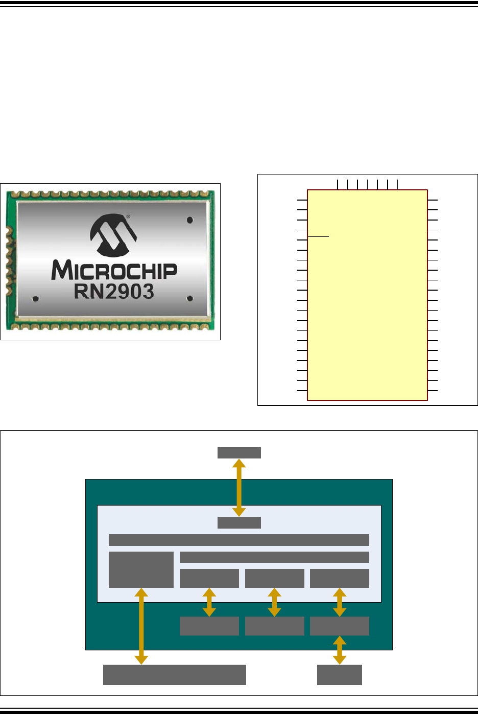
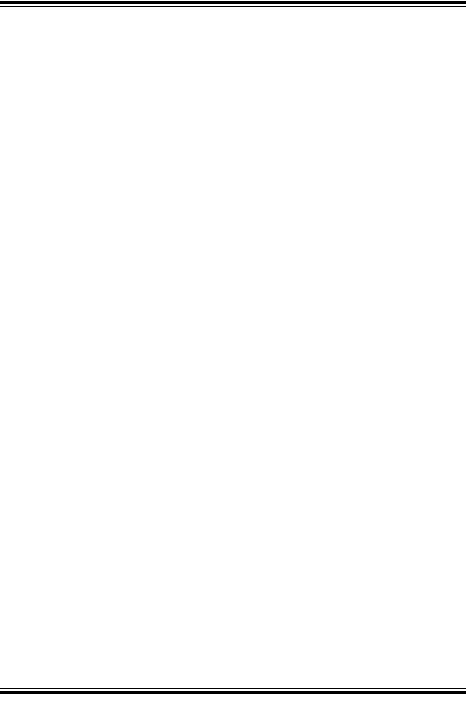
FIGURE 1-1: RN2903 TOP VIEW
LoRa Technology modulation also provides significant
advantages in both blocking and selectivity compared
to the conventional modulation techniques, solving the
traditional design compromise between extended
range, interference immunity, and low-power
consumption.
The RN2903 module delivers exceptional phase noise,
selectivity, receiver linearity, and IIP3 for significantly
lower power consumption. Figure 1-1, Figure 1-2, and
Figure 1-3 show the module’s top view, the pinout, and
the block diagram.
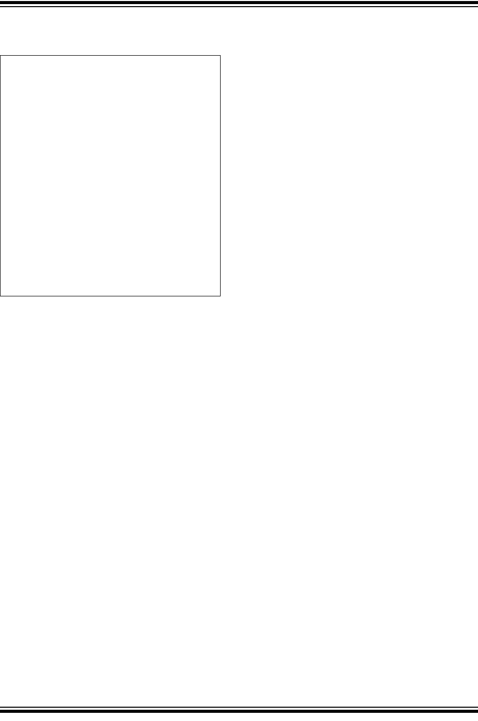
FIGURE 1-2: RN2903 PIN DIAGRAM
FIGURE 1-3: RN2903 BLOCK DIAGRAM
1
GND
2
UART_RTS
3
UART_CTS
4
RESERVED
5
RESERVED
6
UART_TX
7
UART_RX
8
GND
GND
9
GPIO13
10
GPIO12
11
GND
20
GND
12
VDD
13
GPIO11
14
GPIO10
15
NC
16
NC
17
NC
18
NC
19
NC
40
39
38
37
36
35
34
33
32
31
30
21
29
28
27
26
25
24
23
22
GND
GND
GND
GND
GND
GND
RF
NC
VDD
GND
47
46
45
44
43
42
41
GND
NC
TEST0
TEST1
RESET
GPIO0
GPIO1
GPIO2
GPIO3
GPIO4
GPIO5
GPIO6
GPIO7
GPIO8
GPIO9
NC
User Hardware:
Status LEDs, switches, logic IOs, etc.
RN2903 Module
MCU
LoRaTM
Technology radio
Command Processor
14 GPIO Pins Real Time
Clock
LoRaWANTM Protocol Stack
I2CTM SPI
UART
32768 Hz
Crystal
EUI-64
EEPROM
Host MCU
Antenna
915 MHz

RN2903
DS00000A-page 4 Advance Information 2015 Microchip Technology Inc.
Table 1-1 describes the module’s pins.
TABLE 1-1: PIN DESCRIPTION
Pin Name Type Description
1 GND Power Ground supply terminal
2 UART_RTS Output Communication UART RTS signal(1)
3 UART_CTS Input Communication UART CTS signal(1)
4 RESERVED — Do not connect
5 RESERVED — Do not connect
6 UART_TX Output Communication UART Transmit (TX)
7 UART_RX Input Communication UART Receive (RX)
8 GND Power Ground supply terminal
9 GPIO13 Input/Output General purpose I/O pin
10 GPIO12 Input/Output General purpose I/O pin
11 GND Power Ground supply terminal
12 VDD Power Positive supply terminal
13 GPIO11 Input/Output General purpose I/O pin
14 GPIO10 Input/Output General purpose I/O pin
15 NC — Not connected
16 NC — Not connected
17 NC — Not connected
18 NC — Not connected
19 NC — Not connected
20 GND Power Ground supply terminal
21 GND Power Ground supply terminal
22 GND Power Ground supply terminal
23 RF RF analog RF signal pin
24 GND Power Ground supply terminal
25 NC — Not connected
26 GND Power Ground supply terminal
27 GND Power Ground supply terminal
28 GND Power Ground supply terminal
29 NC — Not connected
30 TEST0 — Do not connect
31 TEST1 — Do not connect
32 RESET Input Active-low device Reset input
33 GND Power Ground supply terminal
34 VDD Power Positive supply terminal
35 GPIO0 Input/Output General purpose I/O pin
36 GPIO1 Input/Output General purpose I/O pin
37 GPIO2 Input/Output General purpose I/O pin
38 GPIO3 Input/Output General purpose I/O pin
39 GPIO4 Input/Output General purpose I/O pin
40 GPIO5 Input/Output General purpose I/O pin
41 GND Power Ground supply terminal
42 NC — Not connected
43 GPIO6 Input/Output General purpose I/O pin
2015 Microchip Technology Inc. Advance Information DS00000A-page 5
RN2903
44 GPIO7 Input/Output General purpose I/O pin
45 GPIO8 Input/Output General purpose I/O pin
46 GPIO9 Input/Output General purpose I/O pin
47 GND Power Ground supply terminal
Note 1: Optional handshake lines are supported in future firmware releases.
TABLE 1-1: PIN DESCRIPTION (CONTINUED)
Pin Name Type Description
RN2903
DS00000A-page 6 Advance Information 2015 Microchip Technology Inc.
2.0 GENERAL SPECIFICATIONS
Table 2-1 provides the general specifications for the module. Table 2-2 and Table 2-3 provide the module's electrical
characteristics and current consumption. Table 2-4 and Table 2-5 show the module's dimensions and the RF output
power calibration data.
TABLE 2-1: GENERAL SPECIFICATIONS
Specification Description
Frequency Band 902.000 MHz to 928.000 MHz
Modulation Method FSK, GFSK and LoRa™ Technology modulation
Maximum Over-the-Air Data Rate 300 kbps with FSK modulation; 12500 bps with LoRa Technology modulation
RF connection Board edge connection
Interface UART
Operation Range >15 km coverage at suburban; >5 km coverage at urban area
Sensitivity at 0.1% BER -148 dBm(1)
RF TX Power Adjustable up to max. 20 dBm on 915 MHz band(2)
Temperature (operating) -40°C to +85°C
Temperature (storage) -40°C to +115°C
Humidity 10% ~ 90%
non-condensing
Note 1: Depends on modulation. Expand Spreading Factor (SF).
2: TX power is adjustable. For more information, refer to the “RN2903 LoRa™ Technology Module Command
Reference User’s Guide” (DS40000000A).
TABLE 2-2: ELECTRICAL CHARACTERISTICS
Parameter Min. Typ. Max. Units
Supply Voltage 2.1 — 3.6 V
Voltage on any pin with respect to VSS (except VDD) -0.3 — VDD + 0.3 V
Voltage on VDD with respect to VSS -0.3 — 3.9 V
Input Clamp Current (IIK) (VI < 0 or VI > VDD) — — +/-20 mA
Output Camp Current (IOK) (VO < 0 or VO > VDD) — — +/-20 mA
GPIO sink/source current each — — 25/25 mA
Total GPIO sink/source current — — 200/185 mA
RAM Data Retention Voltage (in Sleep mode or Reset state) 1.5 — — V
VDD Start Voltage to ensure internal Power-on Reset signal — — 0.7 V
VDD Rise Rate to ensure internal Power-on Reset signal 0.05 — — V/ms
Brown-out Reset Voltage 1.75 1.9 2.05 V
Logic Input Low Voltage — — 0.15 x VDD V
Logic Input High Voltage 0.8 x VDD — — V
Input Leakage at <25°C
(VSS<VPIN<VDD, Pin at high-impedance)
—0.150nA
Input Leakage at +60°C
(VSS<VPIN<VDD, Pin at high-impedance)
—0.7100nA
Input Leakage at +85°C
(VSS<VPIN<VDD, Pin at high-impedance)
—4200nA
RF Input Level — — +10 dBm
2015 Microchip Technology Inc. Advance Information DS00000A-page 7
RN2903
TABLE 2-3: CURRENT CONSUMPTION
Mode Typical Current at 3V (mA)
Idle 2.7
RX 13.5
Deep Sleep 0.022
TABLE 2-4: MODULE DIMENSIONS
Parameter Value
Dimensions 17.8 x 26.7 x 3 mm
Weight 2.05g
TABLE 2-5: OUTPUT POWER OF TX
POWER SETTING
TX Power
Setting Output Power
(dBm)
Typical Supply
Current at 3V
(mA)
23.042.6
34.044.8
45.047.3
56.049.6
67.052.0
78.055.0
89.057.7
910.061.0
10 11.0 64.8
11 12.0 73.1
12 13.0 78.0
14 14.7 83.0
15 15.5 88.0
16 16.3 95.8
17 17.0 103.6
20 18.5 124.4
RN2903
DS00000A-page 8 Advance Information 2015 Microchip Technology Inc.
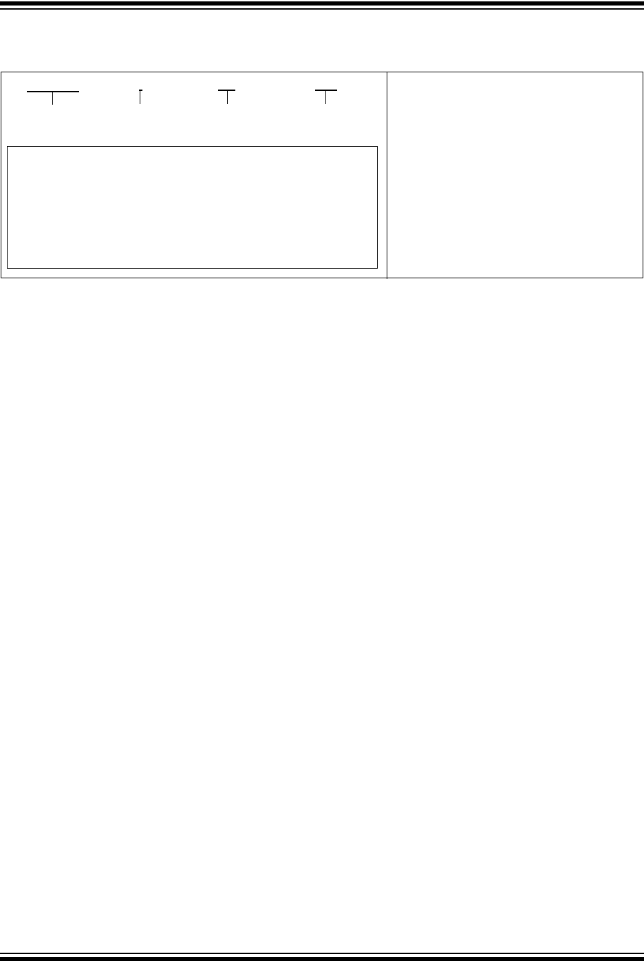
3.0 TYPICAL HARDWARE CONNECTIONS
Figure 3-1 shows the typical hardware connections.
FIGURE 3-1: HARDWARE CONNECTIONS
3.1 INTERFACE TO HOST MCU
The RN2903 module has a dedicated UART interface
to communicate with a host controller. Optional
handshake lines are supported in future firmware
releases. The “RN2903 LoRa™ Technology Module
Command Reference User’s Guide” (DS40000000A)
provides a detailed UART command description.
Table 3-1 shows the default settings for the UART
communication.
3.2 GPIO PINS (GPIO1–GPIO14)
The module has 14 GPIO pins. These lines can be
connected to switches, LEDs, and relay outputs. The
pins are either logic inputs or outputs that can be
accessed via the module firmware. These pins have
limited sink and source capabilities. The current
firmware release only supports output function on all
GPIOs. Electrical characteristics are described in
Table 2-2.
3.3 RF CONNECTION
When routing RF path, use proper strip lines with an
impedance of 50 Ohm.
3.4 RESET PIN
The module’s reset pin is an active-low logic input.
3.5 POWER PINS
It is recommended to connect power pins (Pin 12 and
34) to a stable supply voltage with sufficient source
current. Table 2-2 shows the current consumption.
Additional filtering capacitors are not required but can
be used to ensure stable supply voltage in noisy
environment.
RN2903
GPIOsHost MCU
TX
TXRX
RX
CTS(1) RTS
RTS(1) CTS
RFH
915 MHz band
UART
Status LEDs,
switches,
logic IOs,
etc.
14
Note 1: Optional handshake lines are supported in future firmware releases.
TABLE 3-1: DEFAULT UART SETTINGS
Specification Description
Baud Rate 57600 bps
Packet Length 8 bit
Parity Bit No
Stop Bits 1 bit
Hardware Flow Control No

2015 Microchip Technology Inc. Advance Information DS00000A-page 9
RN2903
4.0 PHYSICAL DIMENSIONS
Figure 4-1 and Figure 4-2 illustrate the physical dimensions and the recommended PCB layout for the RN2903 module.
FIGURE 4-1: RN2903 PHYSICAL DIMENSIONS
FIGURE 4-2: RECOMMENDED PCB FOOTPRINT
Note: Host PCB top layer copper traces must have solder mask to avoid shorting test pins on the bottom of the module.
RN2903
DS00000A-page 10 Advance Information 2015 Microchip Technology Inc.
5.0 APPLICATION INFORMATION
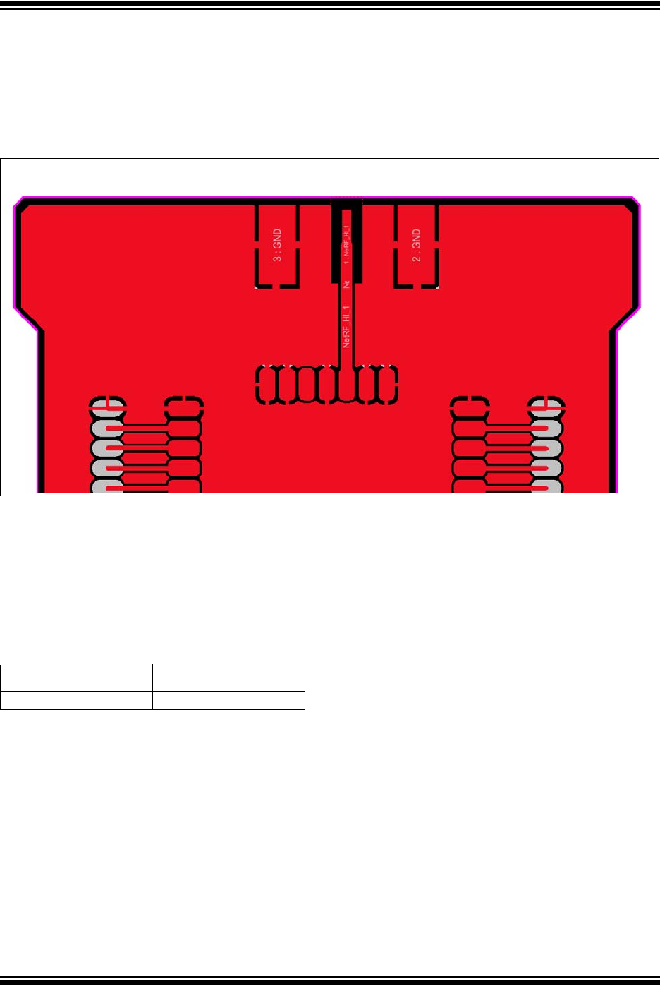
5.1 RF pins and strip line
The RF signals must be routed with properly terminated 50 Ohm strip lines. Use curves instead of sharp corners. Keep
the routing path as short as possible. Figure 5.3 shows a routing example.
FIGURE 5-1: RF ROUTING (EXAMPLE)
5.2 Approved Antennas
Modular certification of the RN2903 module was per-
formed with the external antenna type mentioned in
Table 5-1. Refer to Section 6.0 "Regulatory
Approval" for specific regulatory requirements by
country.
TABLE 5-1: TESTED EXTERNAL
ANTENNA TYPES
Type Gain (dBi)
Dipole 6
2015 Microchip Technology Inc. Advance Information DS00000A-page 11
RN2903
5.3 APPLICATION SCHEMATIC
Figure 5-2 shows the schematic for the RN2903 PICtail™/PICtail Plus Daughter Board.
FIGURE 5-2: PICTAIL™/PICTAIL PLUS DAUGHTER BOARD SCHEMATIC
+3V3
Current measure points
+3V3_M
GND
GNDGND
GND
Module_RX
Module_TX
Module_CTS
Module_RTS
+3V3_M +3V3_M
GND GND GND
+3V3+3V3
GND
GND
GND
GND
+3V3
+3V3
PT_Module_RESET
+3V3
GND
GND
Module_RX
Module_TX
PT_Module_CTS
Module_CTS
+3V3
GND
+3V3
Module_TX
PT_Module_CTS
PT_MCLR
Module_RTS
Module_RTS
GND
CUR1
CUR2
123X45
ID D+ D-+5VGND
USB
G
LD1
Green
G
LD2
Green
D1
B0520LW-7-F
06030R
JP1 06030R
JP2 06030R
JP3 06030R
JP4
06030R
JPI
1
GND
1112
1314
1516
1718
1920
2122
2324
2526
2728
12
34
56
78
910
PICTail
Pin 2.54 mm right angle (PBC14DBDN)
i
50 Ohm
GND
1
2
3
4
5
6
7
8
9
10
11
12
13
14
15
16
17
18
19
20
J1
Socket 1.27 mm
1
2
3
4
5
6
7
8
9
10
11
12
13
14
15
16
17
18
19
20
J2
Socket 1.27 mm
+3V3_ext1
+3V3_ext2
1
0603
1%
R1
Gnd
Vout
4
Pgd
5EN 1
G
n
d
V
out
Pgd
E
N
Vin 2
Gnd
3,6
IC1
MCP1825-3302E/DC
GP0
GP1
GP2
GP3
GP4
GP5
GP6
GP7
GP8
GP9
GP10
GP11
GP12
GP13
PT_Module_RX
PT_Module_RX
1 2
3 4
5 6
7 8
9 10
11 12
13 14
15 16
17 18
19 20
21 22
23 24
25 26
27 28
29 30
PICTail Plus
RA2/AN2/C2IN+/Vref- 1
RA3/AN3/C1IN+/VREF+ 2
RA4/C1OUT/SRQ/T0CKI 3
RA5/AN4/C2OUT/SRNQ/HLVDIN/SS 4
RA7/OSC1/CLKI 6
RA6/OSC2/CLKO 7
RC0/SOSCO/T1CKI/T3CKI/T3G/IOCC0
8
RC1/CCP2/SOSCI/IOCC1
9
RC2/AN14/CTPLS/CCP1/P1A/IOCC2
10
VUSB
11
D-
12 D+
13
RC6/AN18/TX/CK/IOCC6
14
RC7/RX/DT/SDO/IOCC7
15
Vss
Vdd
17
RB0/AN12/SRI/FLT0/SDI/SDA/INT0 18
RB1/AN10/C12IN3-/P1C/SCK/SCL/INT1 19
RB2/AN8/CTED1/P1B/INT2 20
RB3/AN9/C12IN2-/CTED2/CCP2/SDO 21
RB4/AN11/P1D/IOCB4 22
RB5/AN13/T1G/T3CKI/IOCB5 23
RB6/IOCB6/PGC 24
RB7/IOCB7/PGD 25
MCLR/VPP/RE3 26
RA0/AN0/C12IN0- 27
RA1/AN1/C12IN1- 28
EP
29
5,16
RA2
/
AN2
/C
2IN+
/V
ref
-
R
A3/AN3/
C
1IN+/
V
R
E
F+
R
A4
/C
1
OUT
/
SRQ
/T
0C
KI
R
A5
/
AN4
/C
2
OU
T
/
SRN
Q/
H
L
V
DIN
/SS
R
A7
/OSC
1
/CL
KI
R
A6
/OSC
2
/CL
K
O
RC
0
/SOSCO/
T
1C
KI
/T
3C
KI
/T
3G/
I
OCC0
RC
1
/CC
P2
/SOSC
I
/
I
OCC
1
RC
2
/
AN14
/C
T
PL
S/CC
P1
/
P1A
/
I
OCC2
VUS
B
D
-
D+
RC
6
/
AN18
/
TX
/C
K
/
I
OCC
6
RC
7
/
RX
/
DT
/S
D
O/
I
OCC
7
V
ss
Vdd
RB0
/
AN12
/S
RI
/
F
L
T
0/S
DI
/S
DA
/
IN
T
0
RB1
/
AN10
/C
12IN3-
/
P1
C/SC
K
/SCL
/
IN
T
1
R
B2
/
AN8
/C
T
E
D
1
/
P1B
/
IN
T
2
R
B3
/
AN9
/
C12IN2-
/
CT
E
D2
/
CCP2
/
SD
O
R
B4
/
AN11
/
P1D
/
I
OC
B
4
RB5
/
AN13
/
T
1G/
T
3C
KI
/
I
OC
B
5
R
B6
/
I
OC
B6
/
P
GC
RB7
/
I
OC
B7
/
P
GD
M
CL
R/
VPP
/
R
E
3
R
A0
/
AN0
/C
12IN0-
R
A1
/
AN1
/
C12IN1-
E
P
IC2
PIC18LF25K50-I/ML
Module_RX
Module_TX
Module_CTS
Module_RTS
GND
+3V3
GND
IC2_ICSP_MCLR
IC2_ICSP_PGD
IC2_ICSP_PGC
Module_RESET
GND
JP_RST
PT+_SENSE
PT+_SENSE IC2_MCLR
Insert a short on this jumper to keep IC2 in reset state
GND
USB_D+
USB_D-
25V
0603
100nF
C4
25V
0603
470nF
C2
25V
0603
1uF
C1
25V
0603
1uF
C3
6.3V
0603
10uF
C5
50V
0603
10nF
C6
6.3V
0603
4.7uF
C8
4.7k
0603
1%
R8
220
0603
1%
R9
220
0603
1%
R10
220
0603
1%
R4
220
0603
1%
R5
220
0603
1%
R6
+5V_USB
USB_DET
+5V_D
1.5k
0603
1%
R2
100
0603
1%
R7
2.7k
0603
1%
R3
1
2
3
4
5
6
ICSP_IC2
Pin 2.54 mm
1
2
3
4
5
6
TEST
Pin 2.54 mm right angle
GND
+3V3
+3V3
while plugged in PICtail Plus socket
RFH
SMA
GND 1
UART_RTS 2
UART_CTS 3
RESERVED 4
RESERVED 5
UART_TX 6
UART_RX 7
GND 8
GND 11
VDD 12
NC 15
NC 16
NC 17
NC 18
NC 19
GND 20
GND 21
GND 22
RF 23
GND 24
NC 25
GND 26
GND 27
GND
28
NC
29
TEST0
30
TEST1
31
RESET
32
GND
33
VDD
34
GPIO0
35
GND
41
NC
42
GND
47
G
N
D
UA
RT_
RT
S
U
ART
_
CT
S
RE
SE
RVE
D
RE
SE
RV
E
D
UA
RT_
T
X
UA
RT_
RX
G
N
D
G
N
D
VDD
N
C
N
C
N
C
N
C
N
C
G
N
D
G
N
D
G
N
D
R
F
G
N
D
N
C
G
N
D
G
N
D
G
N
D
N
C
T
E
ST
0
T
E
ST
1
RE
S
E
T
G
N
D
VDD
G
PI
O
0
G
N
D
N
C
G
N
D
GPIO1
36
GPIO2
37
GPIO3
38
GPIO4
39
GPIO5
40
GPIO6
43
GPIO7
44
GPIO8
45
GPIO9
46
GPIO11 13
GPIO10 14
GPIO12 10
GPIO13 9
U1
RN2903
Note: Shaded components are not populated by default.

RN2903
DS00000A-page 12 Advance Information 2015 Microchip Technology Inc.
6.0 REGULATORY APPROVAL
This section outlines the regulatory information for the
RN2903 module for the following countries:
• United States
• Canada
• Australia
• New Zealand
6.1 United States
he RN2903 module has received Federal
Communications Commission (FCC) CFR47
Telecommunications, Part 15 Subpart C “Intentional
Radiators” modular approval in accordance with Part
15.212 Modular Transmitter approval. Modular
approval allows the end user to integrate the RN2903
module into a finished product without obtaining
subsequent and separate FCC approvals for
intentional radiation, provided no changes or
modifications are made to the module circuitry.
Changes or modifications could void the user's
authority to operate the equipment. The end user must
comply with all of the instructions provided by the
Grantee, which indicate installation and/or operating
conditions necessary for compliance.
The finished product is required to comply with all
applicable FCC equipment authorizations regulations,
requirements and equipment functions not associated
with the transmitter module portion. For example,
compliance must be demonstrated to regulations for
other transmitter components within the host product;
to requirements for unintentional radiators (Part 15
Subpart B “Unintentional Radiators”), such as digital
devices, computer peripherals, radio receivers, etc.;
and to additional authorization requirements for the
non-transmitter functions on the transmitter module
(i.e., Verification, or Declaration of Conformity) (e.g.,
transmitter modules may also contain digital logic
functions) as appropriate.
6.1.1 LABELING AND USER
INFORMATION REQUIREMENTS
The RN2903 module has been labeled with its own
FCC ID number, and if the FCC ID is not visible when
the module is installed inside another device, then the
outside of the finished product into which the module is
installed must also display a label referring to the
enclosed module. This exterior label can use wording
as follows:
A user's manual for the finished product should include
the following statement:
Additional information on labeling and user information
requirements for Part 15 devices can be found in KDB
Publication 784748 available at the FCC Office of
Engineering and Technology (OET) Laboratory
Division Knowledge Database (KDB)
https://apps.fcc.gov/oetcf/kdb/index.cfm
Contains Transmitter Module FCC ID: T9JRN2903
or
Contains FCC ID: T9JRN2903
This device complies with Part 15 of the FCC Rules.
Operation is subject to the following two conditions:
(1) this device may not cause harmful interference,
and (2) this device must accept any interference
received, including interference that may cause
undesired operation.
This equipment has been tested and found to comply
with the limits for a Class B digital device, pursuant to
part 15 of the FCC Rules. These limits are designed
to provide reasonable protection against harmful
interference in a residential installation. This equip-
ment generates, uses and can radiate radio fre-
quency energy, and if not installed and used in
accordance with the instructions, may cause harmful
interference to radio communications. However,
there is no guarantee that interference will not occur
in a particular installation. If this equipment does
cause harmful interference to radio or television
reception, which can be determined by turning the
equipment off and on, the user is encouraged to try to
correct the interference by one or more of the follow-
ing measures:
• Reorient or relocate the receiving antenna.
• Increase the separation between the equipment
and receiver.
• Connect the equipment into an outlet on a
circuit different from that to which the receiver is
connected.
• Consult the dealer or an experienced radio/TV
technician for help.
2015 Microchip Technology Inc. Advance Information DS00000A-page 13
RN2903
6.1.2 RF EXPOSURE
All transmitters regulated by FCC must comply with RF
exposure requirements. KDB 447498 General RF
Exposure Guidance provides guidance in determining
whether proposed or existing transmitting facilities,
operations or devices comply with limits for human
exposure to Radio Frequency (RF) fields adopted by
the Federal Communications Commission (FCC).
From the RN2903 FCC Grant: Output power listed is
conducted. This grant is valid only when the module is
sold to OEM integrators and must be installed by the
OEM or OEM integrators. This transmitter is restricted
for use with the specific antenna(s) tested in this
application for Certification and must not be co-located
or operating in conjunction with any other antenna or
transmitters within a host device, except in accordance
with FCC multi-transmitter product procedures.
6.1.3 APPROVED EXTERNAL ANTENNA
TYPES
To maintain modular approval in the United States, only
the antenna types that have been tested shall be used.
It is permissible to use different antenna manufacturer
provided the same antenna type and antenna gain
(equal to or less than) is used.
Testing of the RN2903 module was performed with the
antenna types listed in Table 5-1 Tested External
Antenna Types.
6.1.4 HELPFUL WEB SITES
Federal Communications Commission (FCC):
http://www.fcc.gov
FCC Office of Engineering and Technology (OET)
Laboratory Division Knowledge Database (KDB):
https://apps.fcc.gov/oetcf/kdb/index.cfm.
6.2 Canada
The RN2903 module has been certified for use in
Canada under Industry Canada (IC) Radio Standards
Specification (RSS) RSS-210 and RSS-Gen. Modular
approval permits the installation of a module in a host
device without the need to recertify the device.
6.2.1 LABELING AND USER
INFORMATION REQUIREMENTS
Labeling Requirements for the Host Device (from
Section 3.2.1, RSS-Gen, Issue 3, December 2010):
The host device shall be properly labeled to identify the
module within the host device.
The Industry Canada certification label of a module
shall be clearly visible at all times when installed in the
host device, otherwise the host device must be labeled
to display the Industry Canada certification number of
the module, preceded by the words “Contains
transmitter module”, or the word “Contains”, or similar
wording expressing the same meaning, as follows:
User Manual Notice for License-Exempt Radio
Apparatus (from Section 7.1.3 RSS-Gen, Issue 3,
December 2010): User manuals for license-exempt
radio apparatus shall contain the following or
equivalent notice in a conspicuous location in the user
manual or alternatively on the device or both:
Transmitter Antenna (from Section 7.1.2 RSS-Gen,
Issue 3, December 2010): User manuals for
transmitters shall display the following notice in a
conspicuous location:
The above notice may be affixed to the device instead
of displayed in the user manual.
Contains transmitter module IC: 6514A-RN2903.
This device complies with Industry Canada license-
exempt RSS standard(s). Operation is subject to the
following two conditions: (1) this device may not
cause interference, and (2) this device must accept
any interference, including interference that may
cause undesired operation of the device.
Le présent appareil est conforme aux CNR d'Indus-
trie Canada applicables aux appareils radio exempts
de licence. L'exploitation est autorisée aux deux con-
ditions suivantes: (1) l'appareil ne doit pas produire
de brouillage, et (2) l'utilisateur de l'appareil doit
accepter tout brouillage radioélectrique subi, même si
le brouillage est susceptible d'en compromettre le
fonctionnement.
Under Industry Canada regulations, this radio trans-
mitter may only operate using an antenna of a type
and maximum (or lesser) gain approved for the trans-
mitter by Industry Canada. To reduce potential radio
interference to other users, the antenna type and its
gain should be so chosen that the equivalent isotrop-
ically radiated power (e.i.r.p.) is not more than that
necessary for successful communication.
Conformément à la réglementation d'Industrie Can-
ada, le présent émetteur radio peut fonctionner avec
une antenne d'un type et d'un gain maximal (ou
inférieur) approuvé pour l'émetteur par Industrie Can-
ada. Dans le but de réduire les risques de brouillage
radioélectrique à l'intention des autres utilisateurs, il
faut choisir le type d'antenne et son gain de sorte que
la puissance isotrope rayonnée équivalente (p.i.r.e.)
ne dépasse pas l'intensité nécessaire à l'établisse-
ment d'une communication satisfaisante.
RN2903
DS00000A-page 14 Advance Information 2015 Microchip Technology Inc.
User manuals for transmitters equipped with
detachable antennas shall also contain the following
notice in a conspicuous location:
Immediately following the above notice, the
manufacturer shall provide a list of all antenna types
approved for use with the transmitter, indicating the
maximum permissible antenna gain (in dBi) and
required impedance for each.
6.2.2 APPROVED EXTERNAL ANTENNA
TYPES
Transmitter Antenna (from Section 7.1.2 RSS-Gen,
Issue 3, December 2010):
The RN2903 module can only be sold or operated with
antennas with which it was approved. Transmitter may
be approved with multiple antenna types. An antenna
type comprises antennas having similar in-band and
out-of-band radiation patterns. Testing shall be
performed using the highest gain antenna of each
combination of transmitter and antenna type for which
approval is being sought, with the transmitter output
power set at the maximum level. Any antenna of the
same type having equal or lesser gain as an antenna
that had been successfully tested with the transmitter,
will also be considered approved with the transmitter,
and may be used and marketed with the transmitter.
When a measurement at the antenna connector is
used to determine RF output power, the effective gain
of the device's antenna shall be stated, based on
measurement or on data from the antenna
manufacturer. For transmitters of output power greater
than 10 milliwatts, the total antenna gain shall be added
to the measured RF output power to demonstrate
compliance to the specified radiated power limits.
Testing of the RN2903 module was performed with the
antenna types listed in Table 5-1 Tested External
Antenna Types.
6.2.3 HELPFUL WEB SITES
Industry Canada: http://www.ic.gc.ca/
6.3 Australia
RN2903 module RF transmitter test reports can be
used in part to demonstrate compliance in accordance
with ACMA Radio communications "Short Range
Devices" Standard 2004 (The Short Range Devices
standard calls up the AS/NZS 4268:2008 industry
standard). The MRF89XAM9A module test reports can
be used as part of the product certification and
compliance folder. For more information on the RF
transmitter test reports, contact Microchip Technology
Australia office.
AS/NZS 4268:2008 refers to the USA FCC 15.247 RF
standards, the frequency limits of 915 - 928 MHz apply
in Australia.
To meet overall Australian end product compliance, the
integrator must construct a compliance folder
containing all relevant compliance test reports e.g. RF,
EMC, electrical safety and DoC (Declaration of
Conformity) etc. It is the responsibility of the integrator
to know what is required in the compliance folder for
ACMA compliance. For more information on Australia
compliance, refer to the Australian Communications
and Media Authority web site http://www.acma.gov.au/.
6.3.1 HELPFUL WEB SITES
The Australian Communications and Media Authority:
http://www.acma.gov.au/.
This radio transmitter (identify the device by certifica-
tion number, or model number if Category II) has been
approved by Industry Canada to operate with the
antenna types listed below with the maximum permis-
sible gain and required antenna impedance for each
antenna type indicated. Antenna types not included in
this list, having a gain greater than the maximum gain
indicated for that type, are strictly prohibited for use
with this device.
Conformément à la réglementation d'Industrie Can-
ada, le présent émetteur radio peut fonctionner avec
une antenne d'un type et d'un gain maximal (ou
inférieur) approuvé pour l'émetteur par Industrie Can-
ada. Dans le but de réduire les risques de brouillage
radioélectrique à l'intention des autres utilisateurs, il
faut choisir le type d'antenne et son gain de sorte que
la puissance isotrope rayonnée équivalente (p.i.r.e.)
ne dépasse pas l'intensité nécessaire à l'établisse-
ment d'une communication satisfaisante.

2015 Microchip Technology Inc. Advance Information DS00000A-page 15
RN2903
6.4 New Zealand
RN2903 module RF transmitter test reports can be
used in part to demonstrate compliance against the
New Zealand "General User Radio License for Short
Range Devices". New Zealand Radio communications
(Radio Standards) Notice 2010 calls up the AS / NZS
4268:2008 industry standard. The RN2903 module test
reports can be used as part of the product certification
and compliance folder. For more information on the RF
transmitter test reports, contact Microchip Technology.
Information on the New Zealand short range devices
license can be found in the following web links:
http://www.rsm.govt.nz/cms/licensees/types-oflicence/
general-user-licences/short-range-devices
and
http://www.rsm.govt.nz/about-rsm/spectrum-policy
While the AS /NZS 4268:2008 refers to the USA FCC
15.247 and EN 300 220-1 V2.3.1 RF standards, the
frequency limits of 921 MHz to 928 MHz apply in New
Zealand.
To meet overall New Zealand end product compliance,
the developer must construct a compliance folder
containing all relevant compliance test reports e.g. RF,
EMC, electrical safety and DoC (Declaration of
Conformity) etc. It is the responsibility of the developer
to know what is required in the compliance folder for
New Zealand Radio communications. For more
information on New Zealand compliance, refer to the
web site http://www.rsm.govt.nz/.
6.4.1 HELPFUL WEB SITES
Radio Spectrum Ministry of Economic Development:
http://www.rsm.govt.nz/.

RN2903
DS00000A-page 16 Advance Information 2015 Microchip Technology Inc.
NOTES:

2015 Microchip Technology Inc. Advance Information DS00000A-page 17
RN2903
APPENDIX A: REVISION HISTORY
Revision A (June 2015)
This is the initial release of this document.

RN2903
DS00000A-page 18 Advance Information 2015 Microchip Technology Inc.
NOTES:

2015 Microchip Technology Inc. DS00000A-page 19
RN2903
THE MICROCHIP WEB SITE
Microchip provides online support via our WWW site at
www.microchip.com. This web site is used as a means
to make files and information easily available to
customers. Accessible by using your favorite Internet
browser, the web site contains the following
information:
•Product Support – Data sheets and errata,
application notes and sample programs, design
resources, user’s guides and hardware support
documents, latest software releases and archived
software
•General Technical Support – Frequently Asked
Questions (FAQ), technical support requests,
online discussion groups, Microchip consultant
program member listing
•Business of Microchip – Product selector and
ordering guides, latest Microchip press releases,
listing of seminars and events, listings of
Microchip sales offices, distributors and factory
representatives
CUSTOMER CHANGE NOTIFICATION
SERVICE
Microchip’s customer notification service helps keep
customers current on Microchip products. Subscribers
will receive e-mail notification whenever there are
changes, updates, revisions or errata related to a
specified product family or development tool of interest.
To register, access the Microchip web site at
www.microchip.com. Under “Support”, click on
“Customer Change Notification” and follow the
registration instructions.
CUSTOMER SUPPORT
Users of Microchip products can receive assistance
through several channels:
• Distributor or Representative
• Local Sales Office
• Field Application Engineer (FAE)
• Technical Support
Customers should contact their distributor,
representative or Field Application Engineer (FAE) for
support. Local sales offices are also available to help
customers. A listing of sales offices and locations is
included in the back of this document.
Technical support is available through the web site
at: http://microchip.com/support

RN2903
DS00000A-page 20 2015 Microchip Technology Inc.
NOTES:
2015 Microchip Technology Inc. Advance Information DS00000A-page 21
RN2903
PRODUCT IDENTIFICATION SYSTEM
To order or obtain information, e.g., on pricing or delivery, refer to the factory or the listed sales office.
PART NO. IRM XXX
FirmwarePackageTemperature
Range
Device
Device: RN2903: Low-Power Long Range LoRa™ Technology
Transceiver module
Temperature Range: I=-40C to +85C (Industrial)
Package: RM = Radio Module
Examples:
RN2903-I/RM: Industrial temperature
Revision
Number

RN2903
DS00000A-page 22 Advance Information 2015 Microchip Technology Inc.
NOTES:

2015 Microchip Technology Inc. Advance Information DS00000A-page 23
Information contained in this publication regarding device
applications and the like is provided only for your convenience
and may be superseded by updates. It is your responsibility to
ensure that your application meets with your specifications.
MICROCHIP MAKES NO REPRESENTATIONS OR
WARRANTIES OF ANY KIND WHETHER EXPRESS OR
IMPLIED, WRITTEN OR ORAL, STATUTORY OR
OTHERWISE, RELATED TO THE INFORMATION,
INCLUDING BUT NOT LIMITED TO ITS CONDITION,
QUALITY, PERFORMANCE, MERCHANTABILITY OR
FITNESS FOR PURPOSE. Microchip disclaims all liability
arising from this information and its use. Use of Microchip
devices in life support and/or safety applications is entirely at
the buyer’s risk, and the buyer agrees to defend, indemnify and
hold harmless Microchip from any and all damages, claims,
suits, or expenses resulting from such use. No licenses are
conveyed, implicitly or otherwise, under any Microchip
intellectual property rights.
Trademarks
The Microchip name and logo, the Microchip logo, dsPIC,
FlashFlex, flexPWR, JukeBlox, KEELOQ, KEELOQ logo, Kleer,
LANCheck, MediaLB, MOST, MOST logo, MPLAB,
OptoLyzer, PIC, PICSTART, PIC32 logo, RightTouch, SpyNIC,
SST, SST Logo, SuperFlash and UNI/O are registered
trademarks of Microchip Technology Incorporated in the
U.S.A. and other countries.
The Embedded Control Solutions Company and mTouch are
registered trademarks of Microchip Technology Incorporated
in the U.S.A.
Analog-for-the-Digital Age, BodyCom, chipKIT, chipKIT logo,
CodeGuard, dsPICDEM, dsPICDEM.net, ECAN, In-Circuit
Serial Programming, ICSP, Inter-Chip Connectivity, KleerNet,
KleerNet logo, MiWi, MPASM, MPF, MPLAB Certified logo,
MPLIB, MPLINK, MultiTRAK, NetDetach, Omniscient Code
Generation, PICDEM, PICDEM.net, PICkit, PICtail,
RightTouch logo, REAL ICE, SQI, Serial Quad I/O, Total
Endurance, TSHARC, USBCheck, VariSense, ViewSpan,
WiperLock, Wireless DNA, and ZENA are trademarks of
Microchip Technology Incorporated in the U.S.A. and other
countries.
SQTP is a service mark of Microchip Technology Incorporated
in the U.S.A.
Silicon Storage Technology is a registered trademark of
Microchip Technology Inc. in other countries.
GestIC is a registered trademarks of Microchip Technology
Germany II GmbH & Co. KG, a subsidiary of Microchip
Technology Inc., in other countries.
All other trademarks mentioned herein are property of their
respective companies.
© 2015, Microchip Technology Incorporated, Printed in the
U.S.A., All Rights Reserved.
ISBN:
Note the following details of the code protection feature on Microchip devices:
• Microchip products meet the specification contained in their particular Microchip Data Sheet.
• Microchip believes that its family of products is one of the most secure families of its kind on the market today, when used in the
intended manner and under normal conditions.
• There are dishonest and possibly illegal methods used to breach the code protection feature. All of these methods, to our
knowledge, require using the Microchip products in a manner outside the operating specifications contained in Microchip’s Data
Sheets. Most likely, the person doing so is engaged in theft of intellectual property.
• Microchip is willing to work with the customer who is concerned about the integrity of their code.
• Neither Microchip nor any other semiconductor manufacturer can guarantee the security of their code. Code protection does not
mean that we are guaranteeing the product as “unbreakable.”
Code protection is constantly evolving. We at Microchip are committed to continuously improving the code protection features of our
products. Attempts to break Microchip’s code protection feature may be a violation of the Digital Millennium Copyright Act. If such acts
allow unauthorized access to your software or other copyrighted work, you may have a right to sue for relief under that Act.
Microchip received ISO/TS-16949:2009 certification for its worldwide
headquarters, design and wafer fabrication facilities in Chandler and
Tempe, Arizona; Gresham, Oregon and design centers in California
and India. The Company’s quality system processes and procedures
are for its PIC® MCUs and dsPIC® DSCs, KEELOQ® code hopping
devices, Serial EEPROMs, microperipherals, nonvolatile memory and
analog products. In addition, Microchip’s quality system for the design
and manufacture of development systems is ISO 9001:2000 certified.
QUALITYMANAGEMENTS
YSTEM
CERTIFIEDBYDNV
== ISO/TS16949==

DS00000A-page 24 2015 Microchip Technology Inc.
AMERICAS
Corporate Office
2355 West Chandler Blvd.
Chandler, AZ 85224-6199
Tel: 480-792-7200
Fax: 480-792-7277
Technical Support:
http://www.microchip.com/
support
Web Address:
www.microchip.com
Atlanta
Duluth, GA
Tel: 678-957-9614
Fax: 678-957-1455
Austin, TX
Tel: 512-257-3370
Boston
Westborough, MA
Tel: 774-760-0087
Fax: 774-760-0088
Chicago
Itasca, IL
Tel: 630-285-0071
Fax: 630-285-0075
Cleveland
Independence, OH
Tel: 216-447-0464
Fax: 216-447-0643
Dallas
Addison, TX
Tel: 972-818-7423
Fax: 972-818-2924
Detroit
Novi, MI
Tel: 248-848-4000
Houston, TX
Tel: 281-894-5983
Indianapolis
Noblesville, IN
Tel: 317-773-8323
Fax: 317-773-5453
Los Angeles
Mission Viejo, CA
Tel: 949-462-9523
Fax: 949-462-9608
New York, NY
Tel: 631-435-6000
San Jose, CA
Tel: 408-735-9110
Canada - Toronto
Tel: 905-673-0699
Fax: 905-673-6509
ASIA/PACIFIC
Asia Pacific Office
Suites 3707-14, 37th Floor
Tower 6, The Gateway
Harbour City, Kowloon
Hong Kong
Tel: 852-2943-5100
Fax: 852-2401-3431
Australia - Sydney
Tel: 61-2-9868-6733
Fax: 61-2-9868-6755
China - Beijing
Tel: 86-10-8569-7000
Fax: 86-10-8528-2104
China - Chengdu
Tel: 86-28-8665-5511
Fax: 86-28-8665-7889
China - Chongqing
Tel: 86-23-8980-9588
Fax: 86-23-8980-9500
China - Dongguan
Tel: 86-769-8702-9880
China - Hangzhou
Tel: 86-571-8792-8115
Fax: 86-571-8792-8116
China - Hong Kong SAR
Tel: 852-2943-5100
Fax: 852-2401-3431
China - Nanjing
Tel: 86-25-8473-2460
Fax: 86-25-8473-2470
China - Qingdao
Tel: 86-532-8502-7355
Fax: 86-532-8502-7205
China - Shanghai
Tel: 86-21-5407-5533
Fax: 86-21-5407-5066
China - Shenyang
Tel: 86-24-2334-2829
Fax: 86-24-2334-2393
China - Shenzhen
Tel: 86-755-8864-2200
Fax: 86-755-8203-1760
China - Wuhan
Tel: 86-27-5980-5300
Fax: 86-27-5980-5118
China - Xian
Tel: 86-29-8833-7252
Fax: 86-29-8833-7256
ASIA/PACIFIC
China - Xiamen
Tel: 86-592-2388138
Fax: 86-592-2388130
China - Zhuhai
Tel: 86-756-3210040
Fax: 86-756-3210049
India - Bangalore
Tel: 91-80-3090-4444
Fax: 91-80-3090-4123
India - New Delhi
Tel: 91-11-4160-8631
Fax: 91-11-4160-8632
India - Pune
Tel: 91-20-3019-1500
Japan - Osaka
Tel: 81-6-6152-7160
Fax: 81-6-6152-9310
Japan - Tokyo
Tel: 81-3-6880- 3770
Fax: 81-3-6880-3771
Korea - Daegu
Tel: 82-53-744-4301
Fax: 82-53-744-4302
Korea - Seoul
Tel: 82-2-554-7200
Fax: 82-2-558-5932 or
82-2-558-5934
Malaysia - Kuala Lumpur
Tel: 60-3-6201-9857
Fax: 60-3-6201-9859
Malaysia - Penang
Tel: 60-4-227-8870
Fax: 60-4-227-4068
Philippines - Manila
Tel: 63-2-634-9065
Fax: 63-2-634-9069
Singapore
Tel: 65-6334-8870
Fax: 65-6334-8850
Taiwan - Hsin Chu
Tel: 886-3-5778-366
Fax: 886-3-5770-955
Taiwan - Kaohsiung
Tel: 886-7-213-7828
Taiwan - Taipei
Tel: 886-2-2508-8600
Fax: 886-2-2508-0102
Thailand - Bangkok
Tel: 66-2-694-1351
Fax: 66-2-694-1350
EUROPE
Austria - Wels
Tel: 43-7242-2244-39
Fax: 43-7242-2244-393
Denmark - Copenhagen
Tel: 45-4450-2828
Fax: 45-4485-2829
France - Paris
Tel: 33-1-69-53-63-20
Fax: 33-1-69-30-90-79
Germany - Dusseldorf
Tel: 49-2129-3766400
Germany - Munich
Tel: 49-89-627-144-0
Fax: 49-89-627-144-44
Germany - Pforzheim
Tel: 49-7231-424750
Italy - Milan
Tel: 39-0331-742611
Fax: 39-0331-466781
Italy - Venice
Tel: 39-049-7625286
Netherlands - Drunen
Tel: 31-416-690399
Fax: 31-416-690340
Poland - Warsaw
Tel: 48-22-3325737
Spain - Madrid
Tel: 34-91-708-08-90
Fax: 34-91-708-08-91
Sweden - Stockholm
Tel: 46-8-5090-4654
UK - Wokingham
Tel: 44-118-921-5800
Fax: 44-118-921-5820
Worldwide Sales and Service
01/27/15