MINEW TECHNOLOGIES MS50SFB BLE moudle User Manual
SHENZHEN MINEW TECHNOLOGIES CO., LTD. BLE moudle
User Manual

TEL: 0086-755-2103 8160 EMAIL: sales@minewtech.com URL: www.minewtech.com Page 1
BT 5.0 Module MS50SFB Specification
BLE* Module Specification
Model: MS50SFB
Version: V1.0
* Low energy Bluetooth 4.0 and above
1) The Bluetooth trade mark is owned by the Bluetooth SIG Inc. USA.
2) All other trademarks listed herein are owned by their respective owners.
3) All specifications are subject to change without notice.
TEL: 0086-755-2103 8160 EMAIL: sales@minewtech.com URL: www.minewtech.com Page 2
BT 5.0 Module MS50SFB Specification
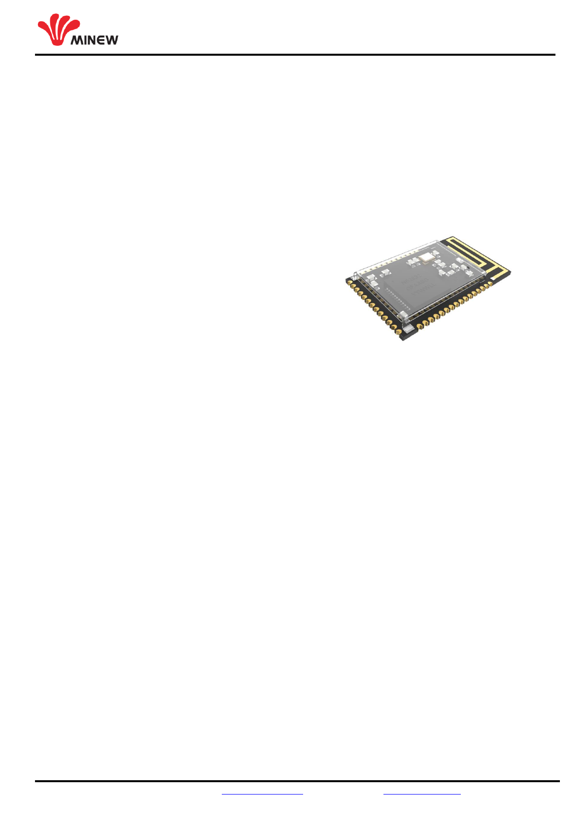
Overview
The MS50SFB is a compact small size Bluetooth 5.0 module with ultra-low power consumption and
optional antenna types; it is very suitable for the coin cell battery powered applications.
The module is highly integrated that contains all the necessary components from radio to different antenna
and a completely implemented Bluetooth protocol stack and pre-flashed UART communication protocol.
Features
• Frequency: 2402 to 2480 MHz
• Max. Output power: +4dBm
• Single power supply: 1.8 – 3.9V
• Range: 10-60 meters
• Chip: nRF52832 (Nordic)
• GPIO Quantity: 32
• 512kB Flash and 64kB RAM
• Module size: 20.0 x 12.0 x 2.0 mm
• NFC type A interface
• ARM Cortex-M4F processor
• Metal shielding with marking
• UART communication protocol (Slave / Master optional)
• 3 optional antenna types: PCB antenna, chip antenna, IPEX connector
• Operating Temperature range: -25 to 85 degree Celsius
Certifications
• CE Certification
• FCC Certification (FCCID: 2ABU6-MS50SFB)
• BQB Certification (QDID: 111267)
Applications
• Cycle computer
• Heart rate monitor
• Blood pressure monitor
• Blood glucose meter
• Weighing machine
• Thermometer
• Mobile accessories
• Sports and fitness sensors
• Remote controllers / Toys
• Key fobs and wrist band
• 3D glasses and gaming controller
MS50SFB
TEL: 0086-755-2103 8160 EMAIL: sales@minewtech.com URL: www.minewtech.com Page 3
BT 5.0 Module MS50SFB Specification
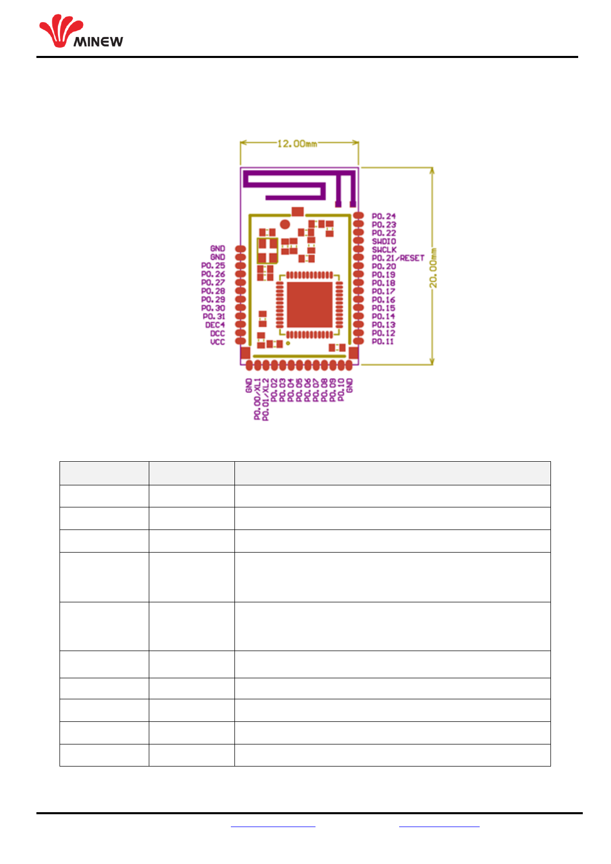
1. Pin Assignment and Description
1.1 Pin assignment
1.2 Pin description
Symbol
Type
Description
VCC
Power
Power supply
DCC
Power
DC/DC converter output pin
GND
Power
Ground
DEC4
Power
1.3V regulator supply decoupling.
Input from DC/DC converter. Output from 1.3 V LDO
SWDIO
Digital I/O
System reset (active low). Hardware debug and flash
programming I/O
programming I/O.
SWCLK
Digital input
Hardware debug and flash programming I/O
P0.00-P0.31
Digital I/O
General purpose I/O pin
XL2
Analog output
Connection for 32.768 kHz crystal
XL1
Analog input
Connection for 32.768 kHz crystal or external 32.768 kHz
RESET
Digital I/O
Configurable as system RESET pin
TEL: 0086-755-2103 8160 EMAIL: sales@minewtech.com URL: www.minewtech.com Page 4
BT 5.0 Module MS50SFB Specification
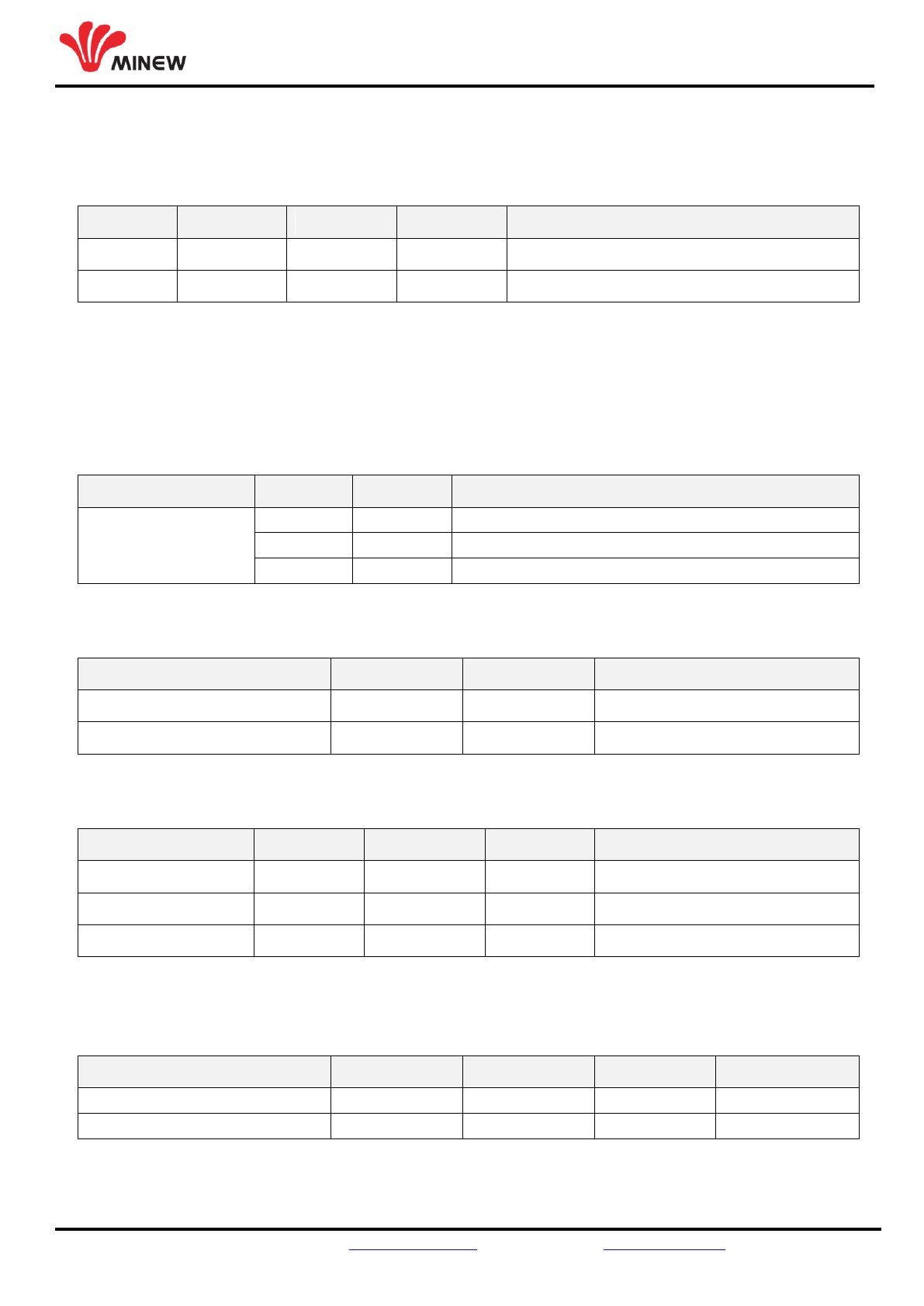
2. Electronic Characteristic
2.1 Absolute maximum ratings
Symbol
Min
Max
Unit
Condition
VCC
1.8
3.9
V
Input DC voltage at VCC pin
ANT
+10
dBm
Input RF power at antenna pin at receiver
Note: The module is not protected against overvoltage or reserved voltages. If necessary, voltage spikes
exceeding the power supply voltage specification must be limited to values within the specified
boundaries by using appropriate protection devices.
2.2 Maximum ESD ratings
Parameter
Max
Unit
Remarks
ESD Sensitivity
4
KV
Human body model
750
V
Charged device model
+/- 8
KV
ESD indirect contact discharge
2.3 Operating temperature range
Parameter
Min
Max
Unit
Storage temperature
-40
85
℃
Operating temperature
-40
85
℃
2.4 Current consumption
Parameter
Min
Max
Unit
Remark
Receiving current
5.4
mA
standard mode
Transmission power
5.3
mA
transmission power at 0dbm
Sleeping current
1
uA
power mode 3
2.5 RF performance
Parameter
Min
Typical
Max
Unit
Receiver input sensitivity
-93
dBm
Output power
-30
0
+4
dBm
TEL: 0086-755-2103 8160 EMAIL: sales@minewtech.com URL: www.minewtech.com Page 5
BT 5.0 Module MS50SFB Specification
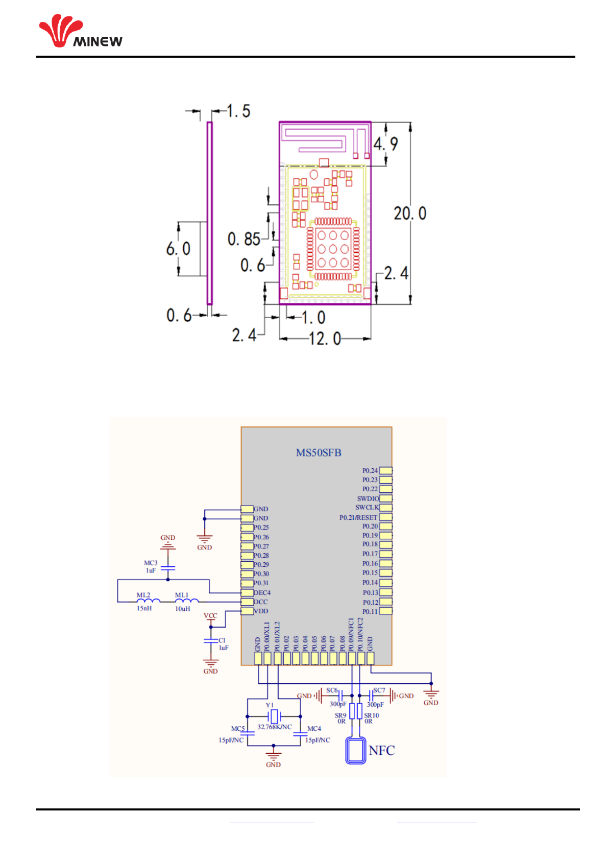
3. Physical Dimension
Unit: mm
4. Reference Schematic Design
Unit: mm
TEL: 0086-755-2103 8160 EMAIL: sales@minewtech.com URL: www.minewtech.com Page 6
BT 5.0 Module MS50SFB Specification
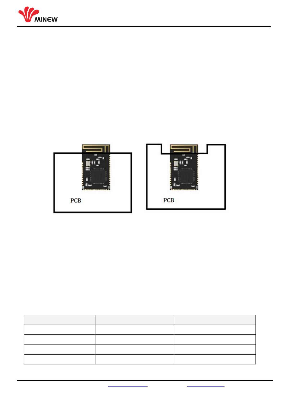
5. Layout and Soldering Considerations
To make sure wireless performance is at its best condition, please layout the module on the
carrier board as below instructions.
5.1 Carrier board under the antenna area of the module like the picture;
5.2 Keep out enough area for the antenna area;
5.3 Reflow profiles are to be selected according to standard manufacturing process;
5.4 The soldering temperature should be less than 206℃;
5.5 The module should be placed far away other low frequency and digital circuits;
5.6 The MS50 series modules contain highly sensitive electronic circuitry and are Electrostatic
Sensitive Devices (ESD). Handling the MS50 series modules without proper ESD protection
may destroy or damage them permanently.
Recommended Layout for the Carrier Board
*PCB: It’s the mother board / carrier board.
6. UART Commands
Please refer to the UART commands document to know more.
7. Package
Details
Tray
Carton
Quantity (module)
80 pcs
4000 pcs / 50 trays
Net Weight
40.0g
4.5Kg
Gross Weight
75.0g
9.5Kg
Size
20 x 18 x 5 cm
32 x 23 x 40 cm
TEL: 0086-755-2103 8160 EMAIL: sales@minewtech.com URL: www.minewtech.com Page 7
BT 5.0 Module MS50SFB Specification
8. Ordering information
Ordering number
Description
306030058
MS50SFB-001, nRF52832 BT 5.0 Module, PCB Antenna, UART function
306030059
MS50SFB-002, nRF52832 BT 5.0 Module, Chip Antenna, UART function
306030060
MS50SFB-003, nRF52832 BT 5.0 Module, IPEX connector for external antenna,
UART function
<END>
FCC Caution:
This device complies with part 15 of the FCC Rules. Operation is subject to the following two
conditions: (1) this device may not cause harmful interference, and (2) this device must accept
any interference received, including interference that may cause undesired operation.
Any changes or modifications not expressly approved by the party responsible for compliance
could void the user's authority to operate the equipment.
NOTE: This equipment has been tested and found to comply with the limits for a Class B
digital device, pursuant to Part 15 of the FCC Rules. These limits are designed to provide
reasonable protection against harmful interference in a residential installation. This equipment
generates, uses and can radiate radio frequency energy and, if not installed and used in
accordance with the instructions, may cause harmful interference to radio communications.
However, there is no guarantee that interference will not occur in a particular installation.
If this equipment does cause harmful interference to radio or television reception,
which can be determined by turning the equipment off and on, the user is encouraged to try to
correct the interference by one or more of the following measures:
-- Reorient or relocate the receiving antenna.
-- Increase the separation between the equipment and receiver.
-- Connect the equipment into an outlet on a circuit different
from that to which the receiver is connected.
-- Consult the dealer or an experienced radio/TV technician for help.
To maintain compliance with FCC’s RF Exposure guidelines, This equipment should be
installed and operated with minimum distance between 20cm the radiator your body: Use
only the supplied antenna.