MXCHIP Information Technology EMB1061 BLE module User Manual
Shanghai MXCHIP Information Technology Co.,Ltd. BLE module Users Manual
User Manual
Shanghai MXCHIP Information Technology Co., Ltd.
9th Floor, No.5, Lane2145 JinshaJiang Road Putuo District, ShangHai.(200333)Tel.: 021-52655026 Website: http://mxchip.com/
Track Number: AN0092EN
MXCHIP Co., Ltd
Version: 1.0
2017.7.11
Category: Application Note
Open
EMB1061 Hardware Design Guide
Abstract
This document lists the consideration in each step during designing product with MXCHIP module. In order
to achieve rapid mass production, Users should be familiar with the document to pre-consider and avoid problems
effectively in designing, producing, programming and testing.
More Help
For more products information please visit: http://mxchip.com/
For more development data please go to MiCO developer bbs: http://mico.io/
For more Fogcloud data please go to Fogcloud developer center: http://easylink.io/
Copyright Notice
Mxchip copyrights this specification. No part of this specification may be reproduced in any form or
means(specially brand, type name, part number and pictures), without the prior written consent of Mxchip.
Application Note [Page 1]
EMB1061 Hardware Design Guide
Version Record
Date
Version
Details
2017-7-11
V1.0
Initial release

Application Note [Page 2]
EMB1061 Hardware Design Guide
目录
EMB1061 Hardware Design Guide.....................................................................................................................................1
Version Record...................................................................................................................................................................... 1
1. Introduction.......................................................................................................................................................................3
2. Hardware Design Guide................................................................................................................................................... 6
2.1 MECHANICAL SIZE.................................................................................................................................................... 6
2.1.1 EMB1061 Pin Definition........................................................................................................................... 6
2.2 REFERENCE PCB PACKAGE DESIGN......................................................................................................................... 7
2.3 DC POWER DESIGN................................................................................................................................................... 7
2.4 RF DESIGN................................................................................................................................................................ 8
2.4.1 On-board PCB Antenna Design.................................................................................................................8
2.4.2 External Antenna........................................................................................................................................9
2.5 ESD DESIGN............................................................................................................................................................10
3. Downloading Firmware.................................................................................................................................................. 11
4. Important Statement...................................................................................................................................................... 12
5. SMT..................................................................................................................................................................................13
5.1 STENCILS................................................................................................................................................................. 13
5.2 TEMPERATURE CURVE OF REFLOW......................................................................................................................... 14
6. reference design...............................................................................................................................................................15
7. Technical Support........................................................................................................................................................... 17
Figure Content
Figure 1.1. Top view of EMB1061.........................................................................................................................3
Figure 1.2 Hardware Block.................................................................................................................................... 5
Figure 2.1 Top View of Mechanical Size (Unit:mm)............................................................................................. 6
Figure 2.2 Minimum PCB Clearance Area............................................................................................................ 9
Figure 2.3 Position of the Module..........................................................................................................................9
Figure 2.4 Size of connector for external antenna.............................................................................................. 10
Figure 5.1 Stencils size......................................................................................................................................... 13
Figure 5.2 Temperature Curve of Secondary Reflow...........................................................................................14
Application Note [Page 3]
EMB1061 Hardware Design Guide
1. Introduction
This document lists the consideration in each step during designing product with MXCHIP module. In order
to achieve rapid mass production, Users should be familiar with the document to pre-consider and avoid problems
effectively in designing, producing, programming and testing.
Suitable module type:
EMB1061
Phase to attention:
Hardware design;
Firmware downloading;
Firmware testing;
SMT;
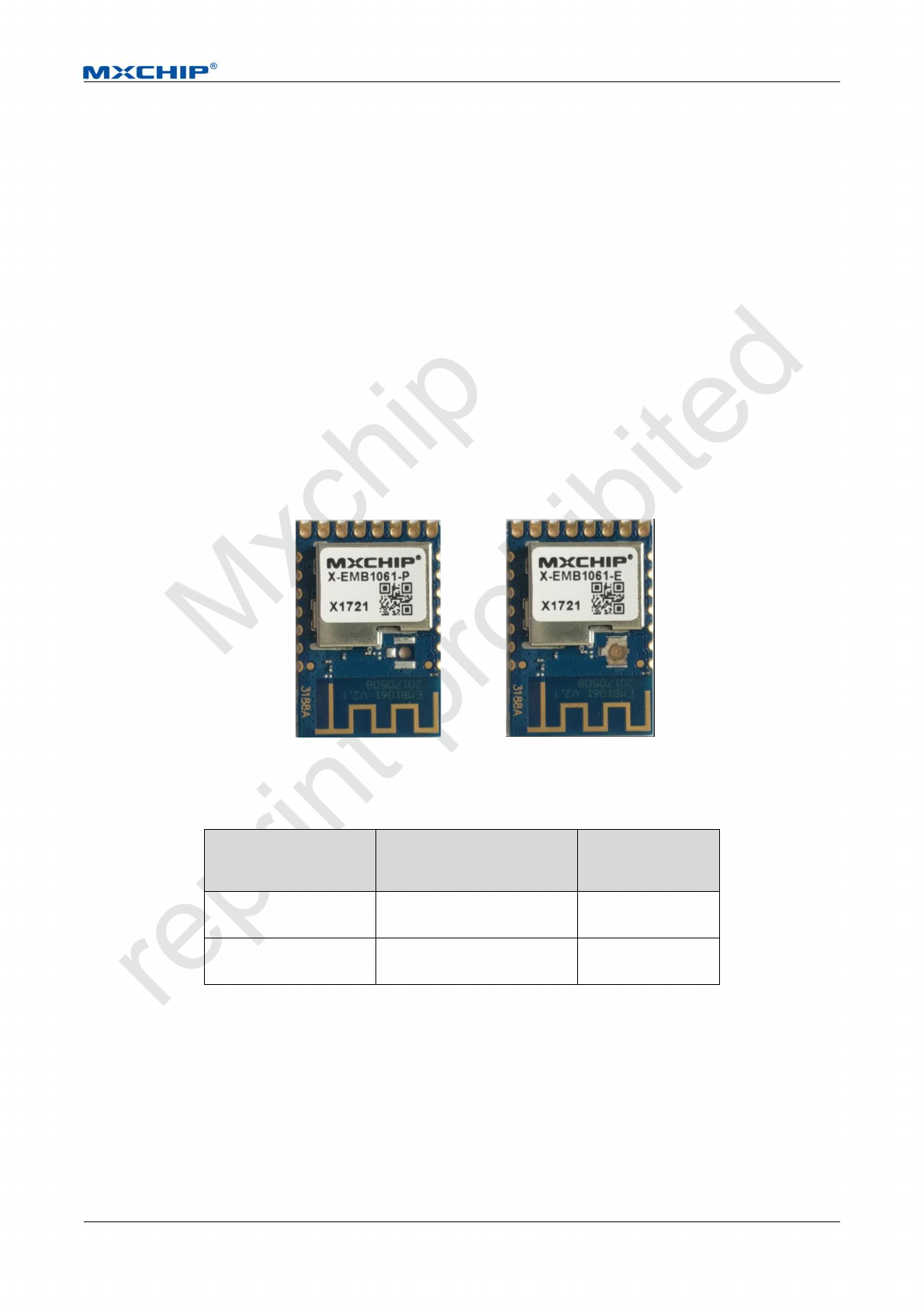
Top view of EMB1061
Figure 1.1. Top view of EMB1061
EMB1061
Module type
Antenna Type
Illustration
EMB1061-P
On-board PCB
Default
EMB1061-E
IPEX
Optional
EMB1061 has two types of antenna: PCB antenna (EMB1061-P), IPEX connector (EMB1061-E).
Application Note [Page 4]
EMB1061 Hardware Design Guide
EMB1061-P
Application Note [Page 5]
EMB1061 Hardware Design Guide
EMB1061-E
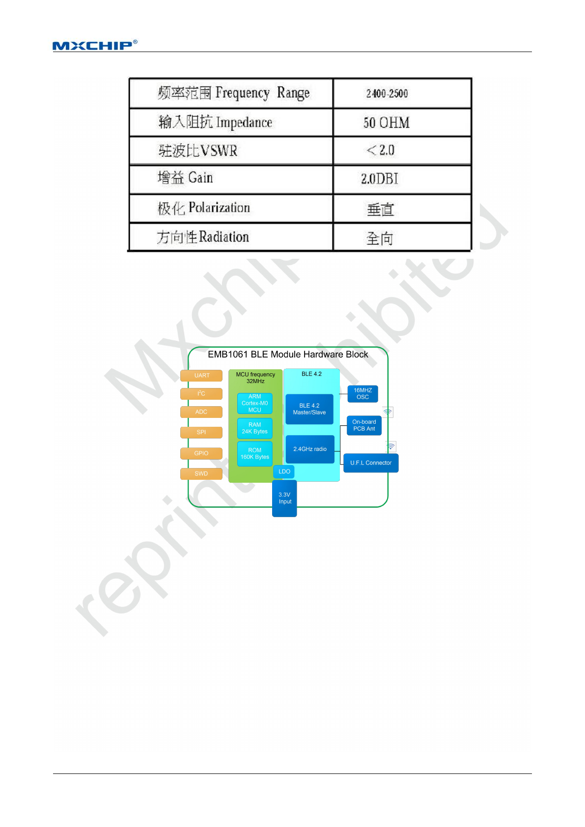
Hardware Block
Figure 1.2 Hardware Block
Application Note [Page 6]
EMB1061 Hardware Design Guide
2. Hardware Design Guide
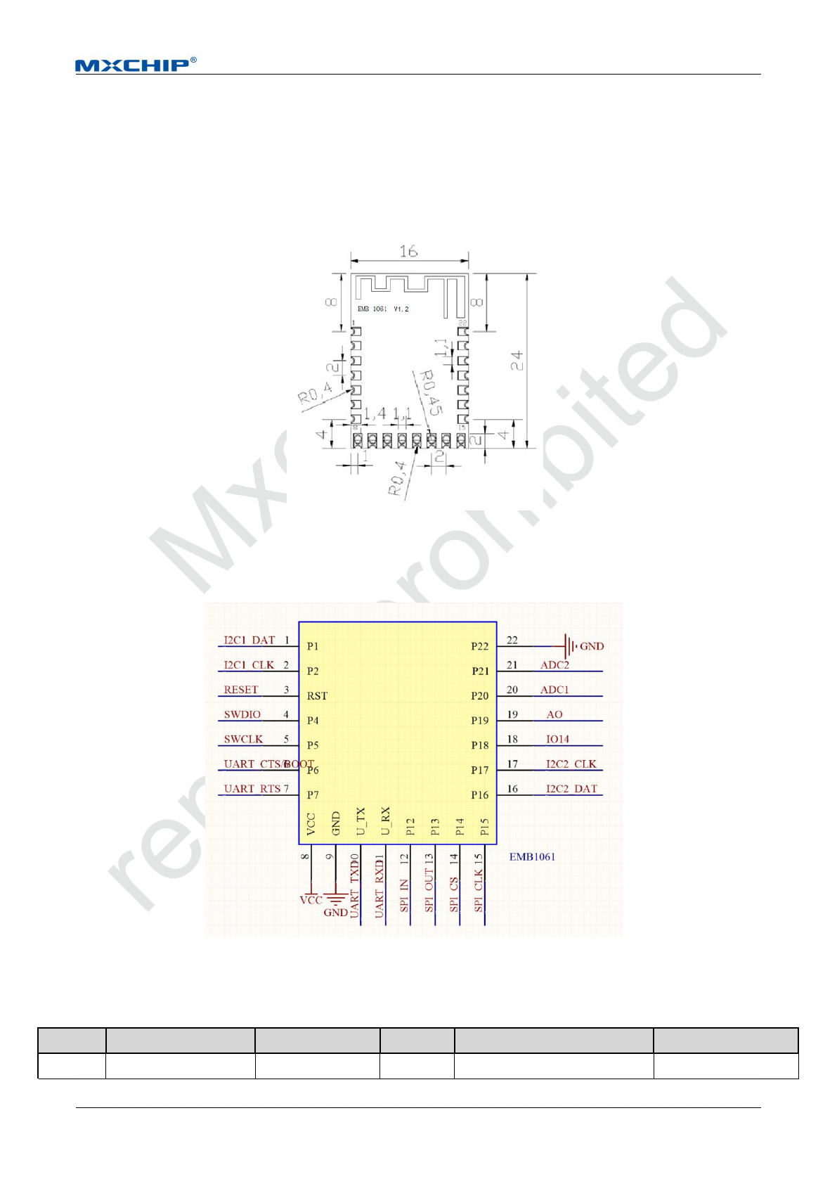
2.1 Mechanical Size
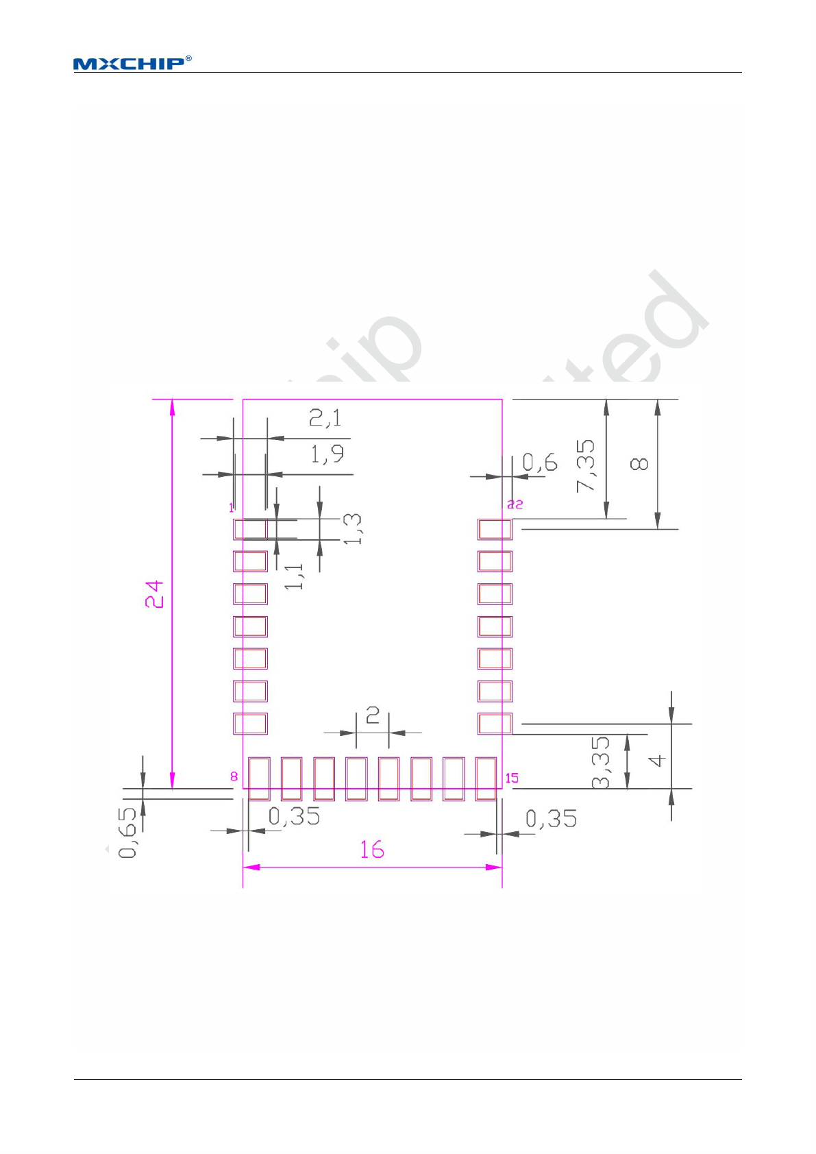
Mechanical size of EMB1061 (Unit: mm)
Figure 2.1 Top View of Mechanical Size (Unit:mm)
EMB1061 Package Definition
2.1.1 EMB1061 Pin Definition
Table 1 EMB1061 Pin Definition
NO.
Name
Pin of ST SOC
Type
Main function
Alternative function
1
I2C1 DAT
IO13
I/O
I2C1 DAT
GPIO13
Application Note [Page 7]
EMB1061 Hardware Design Guide
NO.
Name
Pin of ST SOC
Type
Main function
Alternative function
2
I2C1 CLK
IO12
I/O
I2C1 CLK
GPIO12
3
RESET
RESETN
Input
Reset
4
SWDIO
IO10
I/O
SWDIO
GPIO10
5
SWCLK
IO9
I/O
SWCLK
GPIO9
6
UART CTS/BOOT
IO7
I/O
UART CTS/BOOT
I2C2_DAT
7
UART RTS
IO6
I/O
UART RTS
I2C2_CLK
8
VCC
VBAT2
S
POWER_SUPPLY
9
GND
GND
S
GND
10
UART_TX
IO8
I/O
USER_UART_TX
SPI_CLK
11
UART_RX
IO11
I/O
USER_UART_RX
GPIO11
12
SPI IN
IO3
I/O
SPI IN
PWM1
13
SPI OUT
IO2
I/O
SPI OUT
PWM0
14
SPI CS
IO1
I/O
SPI CS
GPIO1
15
SPI CLK
IO0
I/O
SPI CLK
GPIO0
16
I2C2 DAT
IO5
I/O
I2C2 DAT
PWM1
17
I2C2 CLK
IO4
I/O
I2C2 CLK
PMW0
18
IO14
IO14
I/O
GPIO14
Analog Output
19
AO
ANATEST1
O
Analog Output
Analog Output
20
ADC1
ADC1
I
ADC1
ADC INPUT
21
ADC2
ADC2
I
ADC2
ADC INPUT
22
GND
GND
S
GND
2.2 Reference PCB Package Design
Figure 2.1 is the reference module package design for baseplate PCB design.
Solder mask openness can be the same size with EMB1061’s pad. EMB1061’s PCB thickness is 1.0mm.
2.3 DC Power Design
EMB1061’s operation voltage is 1.7~3.6V with typical voltage 3.3V. The peak current of the module is about
10mA.
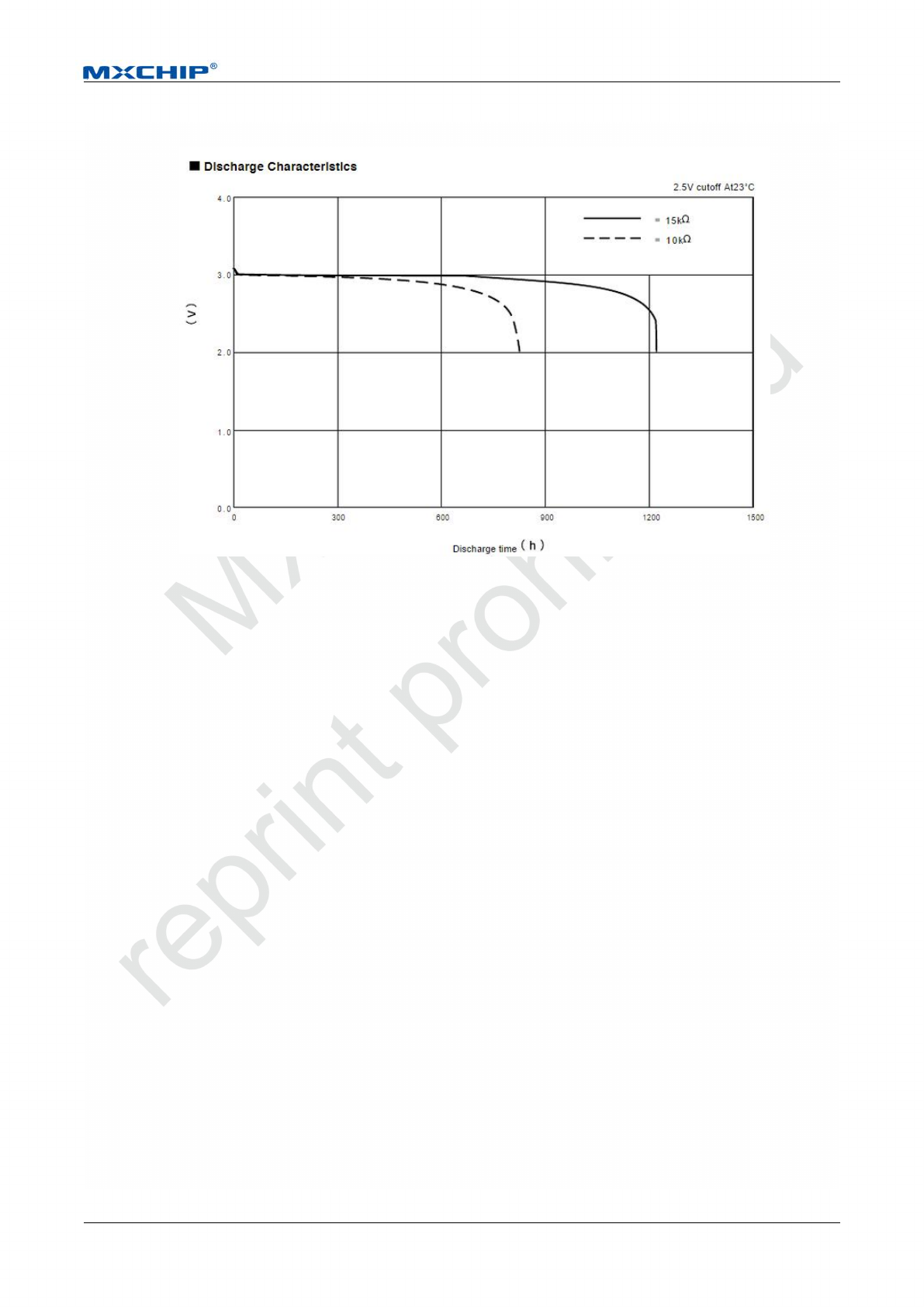
If powered by battery, please pay attention to the max voltage and minimal discharge voltage. For coin cell,
the typical voltage is 3.0V, and the minimal discharge voltage is 2.0V, and in practice it usually end up discharging
at about 2.5V. For example, CR2032 coin cell, the discharge characteristics is as below picture. When choosing
Application Note [Page 8]
EMB1061 Hardware Design Guide
battery, please check whether its discharge characteristics is suitable for EMB1061.
If using DC-DC, DC-DC’s output voltage should be 3.3V, and it’s max current should be above 20mA. PCB
route should be particularly aware for DC/DC power supply. Compact element, excellent connection between
input and output ground, long distance between feedback signal and inductance and Schottky diode are required
for route. Details about the requirements should refer to the datasheet of DC/DC device.
Maximum output current and dissipate heat should be aware for the using of LDO. For example, voltage drop
is 1.7V when voltage reduces from 5V to 3.3V. If the current is 100mA, power consumption is 1.7V *
100mA=170mW. Power Dissipation is a parameter of LDO, which should be over 170mW.
2.4 RF Design
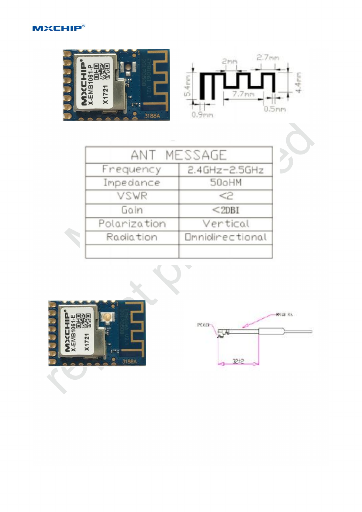
2.4.1 On-board PCB Antenna Design
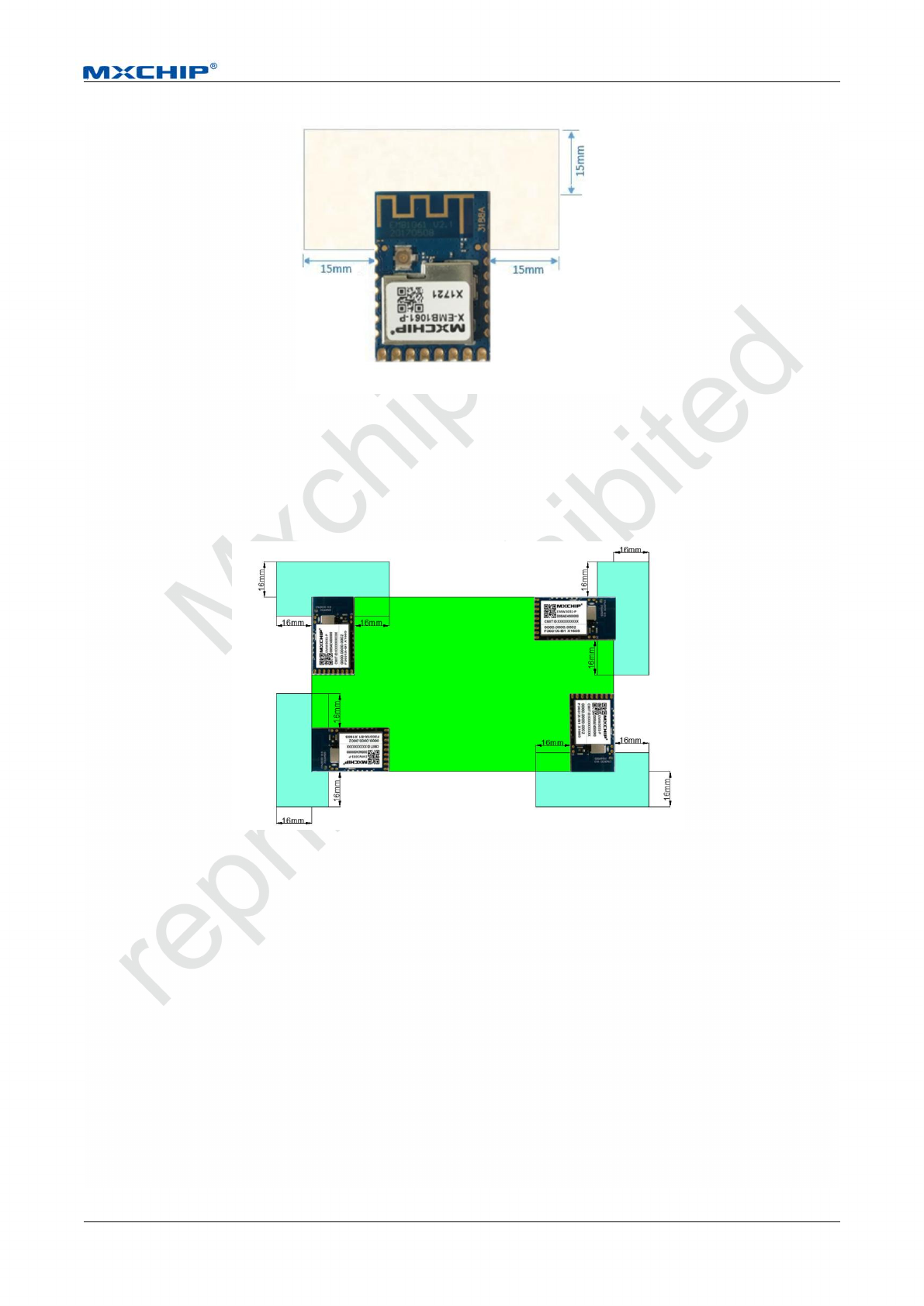
There should not be components, or ground, or circuit 15mm away from EMB1061’s PCB antenna.
Application Note [Page 9]
EMB1061 Hardware Design Guide
Figure 2.2 Minimum PCB Clearance Area
In order to reduce the influence from metal components to PCB antenna and wireless signal, it is better to
mount EMB1061 on these areas, as shown in figure 2.3.
Figure 2.3 Position of the Module
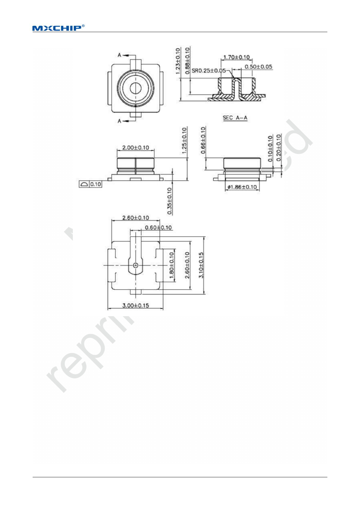
2.4.2 External Antenna
Size of connector for external antenna is shown in figure 2.4. Make sure the correct size with suppliers before
buying the connectors of antenna.
Application Note [Page 10]
EMB1061 Hardware Design Guide
Figure 2.4 Size of connector for external antenna
2.5 ESD Design
ESD level of the module: Human body model (HBM) is 2000V, charged device model (CDM) is 500V.
Position of ESD protected components should be reserved if the products require higher ESD requirement.
Application Note [Page 11]
EMB1061 Hardware Design Guide
3. Downloading Firmware
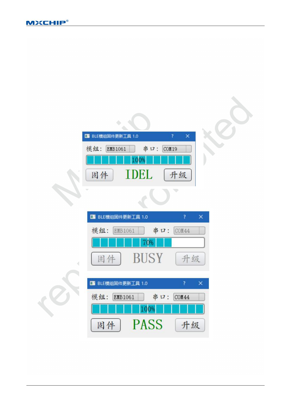
1. Unzip the package and install the USB driver "CDM 2.08.30 WHQL Certified_64".
2.Power supply to the development board through USB interface. View its corresponding serial port number
from device Manager. 3. Enter BOOTLOADER mode. After confirming that the module is powered (a red LED
lights up next to the USB port), hold down the BOOT button and reset the module through the Reset button, then
release the BOOT button. If the operation succeeds, EMB1061 enters BootLoader mode. 4. Open firmware
upgrade tool software, select module EMB1061, select user serial port number and fix A document.
5. Select the firmware file to upgrade (click the firmware button), and if everything is normal, you will see
the upgrade button brighten. Indicates that you can upgrade. Hover over the firmware button to see the absolute
path of the firmware that has been selected. As shown in the figure:
6. Click the upgrade button and a dialog box will pop up to prompt the user to confirm that the module is now
in BootLoader mode. Click OK to start the upgrade, as shown in figure:
7. After a successful upgrade, the module will automatically Reset and run from the latest firmware. If there
is an error in the upgrade process, the tool will pop up an error prompt, according to which the user can further
process.

Application Note [Page 12]
EMB1061 Hardware Design Guide
4. Important Statement
MXCHIP has a duty to make sure there is no quality problem when sell the module to customers.
Customers have the rights to ask MXCHIP to exchange goods if the product has quality problem.
If the customer find the problem after welding the module on board without testing at the beginning,
MXCHIP is only responsible for the compensation of the module part.
MXCHIP would help customers solve technical problem in developing firmware without save any MVA/bin
file. Customers should save different development vision and download relative vision in module before
producing.
Application Note [Page 13]
EMB1061 Hardware Design Guide
5. SMT
5.1 Stencils
Stencils thickness is suggested to be 0.12mm (0.1~0.15mm) with Laser grinding. Recommended solder paste:
No lead SAC305.
Stencils size is shown in figure 5.1, pad holes extend 0.15mm in order to improving solder wicking. Solder
mask’s width should be 0.1mm wider than stencil’s paste layer, like Pin1 of Figure 5.1. So that if there is no AOI
testing, you can check whether the module is placed well by eye to reduce the Pseudo Soldering.
There is EMB1061’s PCB lib in mxchip.com, and you can use it directly.
Figure 5.1 Stencils size
Application Note [Page 14]
EMB1061 Hardware Design Guide
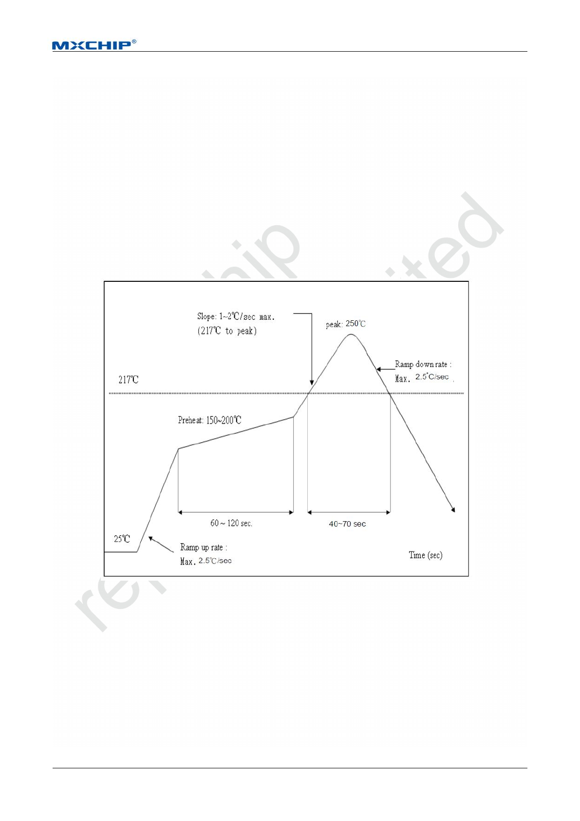
5.2 Temperature Curve of Reflow
Pseudo soldering could be reduced by control the furnace with temperature curve of secondary reflow, as
shown in figure 5.2.
Secondary reflow times should be less than twice.
1. Max Rising Slope : 3℃/sec
2. Max Falling Slope: -3 ℃/sec
3. Preheat Time(150℃~200℃): 60sec~120sec
4. Over 217℃Time:40sec~70sec
5. Peak Temp.240℃~250℃
Figure 5.2 Temperature Curve of Secondary Reflow
Application Note [Page 15]
EMB1061 Hardware Design Guide
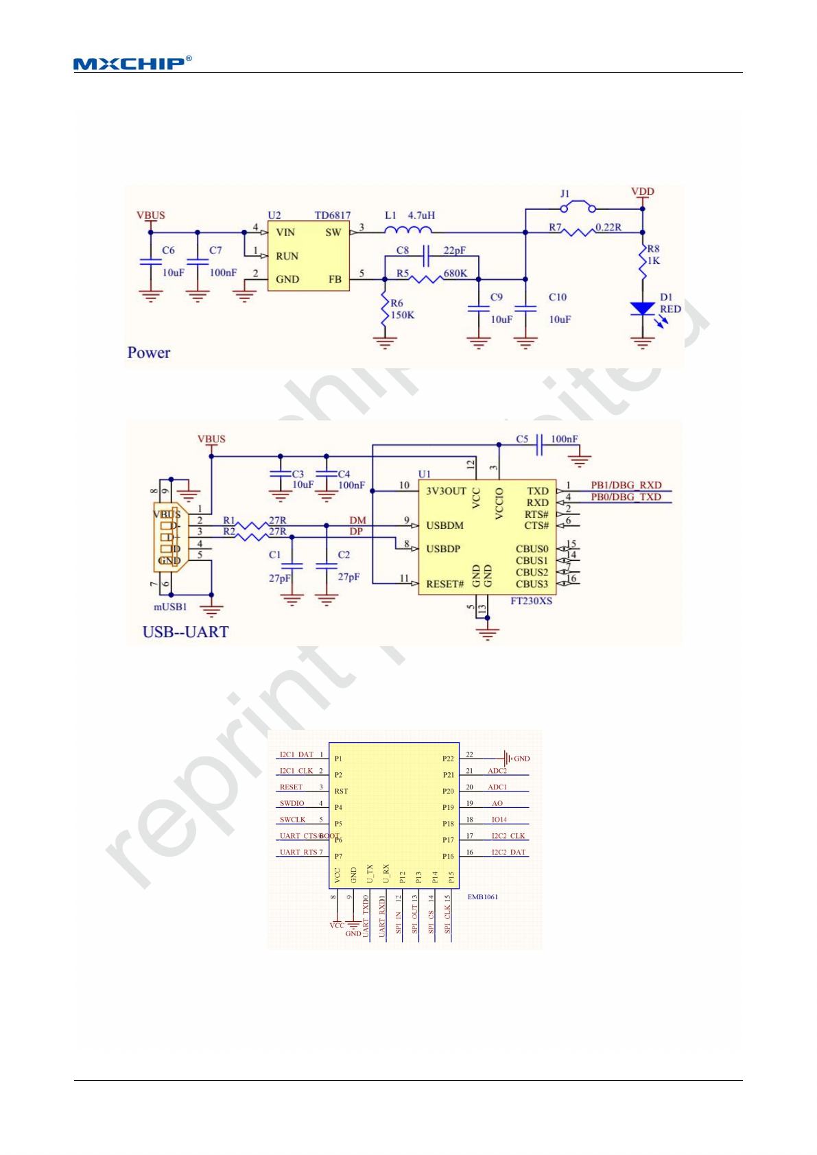
6. reference design
Power source circuit
USB to UART
Figure 12 USB to UART
external interface circuit
Figure 13 External Interface Circuit of EMB1061
Voltage of EMB1061 UART is 3.3V. 5V UART should convert to 3.3V UART for the users that have 5V
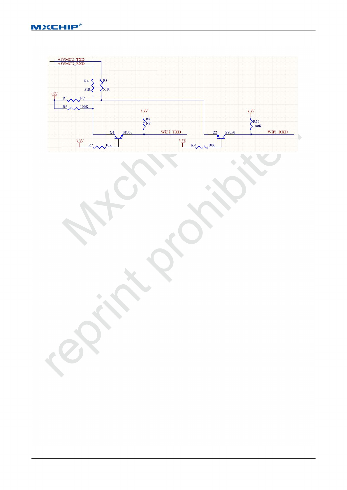
Application Note [Page 16]
EMB1061 Hardware Design Guide
chips. Convert circuit is shown in figure 14.
Figure 14 3.3V UART- 5V UART Convert Circuit
Application Note [Page 17]
EMB1061 Hardware Design Guide
7. Technical Support
For consultation or purchase the product, please contact Mxchip during working hours:
From Monday to Friday, morning 9:00~12:00, afternoon 13:00~18:00
Telephone: +86-21-52655026
Contact address: 9th Floor, No.5, Lane2145 JinshaJiang Road Putuo District, ShangHai.
Postcode:200333
Email: sales@mxchip.com

Application Note [Page 1]
EMB1061 Hardware Design Guide
FCC Regulations:
This device complies with part 15 of the FCC Rules. Operation is subject to the following two
conditions: (1) This device may not cause harmful interference, and (2) This device must accept any
interference received, including interference that may cause undesired operation.
This device has been tested and found to comply with the limits for a Class B digital device ,
pursuant to Part 15 of the FCC Rules. These limits are designed to provide reasonable protection
against harmful interference in a residential installation. This equipment generates, uses and can
radiated radio frequency energy and, if not installed and used in accordance with the instructions,
may cause harmful interference to radio communications. However, there is no guarantee that
interference will not occur in a particular installation If this equipment does cause harmful
interference to radio or television reception, which can be determined by turning the equipment off
and on, the user is encouraged to try to correct the interference by one or more of the following
measures:
-Reorient or relocate the receiving antenna.
-Increase the separation between the equipment and receiver.
-Connect the equipment into an outlet on a circuit different from that to which the receiver is
connected.
-Consult the dealer or an experienced radio/TV technician for help.
Caution: Changes or modifications not expressly approved by the party responsible for
compliance could void the user‘s authority to operate the equipment.
RF Exposure Information
This device complies with FCC radiation exposure limits set forth for an uncontrolled
environment. In order to avoid the possibility of exceeding the FCC radio frequency exposure limits,
human proximity to the antenna shall not be less than 20cm (8 inches) during normal operation.
IMPORTANT NOTE:
This module is intended for OEM integrator. The OEM integrator is still responsible for the FCC
compliance requirement of the end product, which integrates this module. 20cm minimum distance
has to be able to be maintained between the antenna and the users for the host this module is
integrated into. Under such configuration, the FCC radiation exposure limits set forth for an
population/uncontrolled environment can be satisfied.
Any changes or modifications not expressly approved by the manufacturer could void the user's
authority to operate this equipment.

Application Note [Page 2]
EMB1061 Hardware Design Guide
USERS MANUAL OF THE END PRODUCT:
In the users manual of the end product, the end user has to be informed to keep at least 20cm
separation with the antenna while this end product is installed and operated. The end user has to be
informed that the FCC radio-frequency exposure guidelines for an uncontrolled environment can be
satisfied. The end user has to also be informed that any changes or modifications not expressly
approved by the manufacturer could void the user's authority to operate this equipment. If the size of
the end product is smaller than 8x10cm, then additional FCC part 15.19 statement is required to be
available in the users manual: This device complies with Part 15 of FCC rules. Operation is subject to
the following two conditions: (1) this device may not cause harmful interference and (2) this device
must accept any interference received, including interference that may cause undesired operation.
LABEL OF THE END PRODUCT:
The final end product must be labeled in a visible area with the following " Contains Transmitter
Module FCC ID: P53-EMB1061 ". If the size of the end product is larger than 8x10cm, then the
following FCC part 15.19 statement has to also be available on the label: This device complies with
Part 15 of FCC rules.
Operation is subject to the following two conditions: (1) this device may not cause harmful
interference and (2) this device must accept any interference received, including interference that
may cause undesired operation.