MXCHIP Information Technology EMW3239 Embedded WiFi and Bluetooth module User Manual
Shanghai MXCHIP Information Technology Co.,Ltd. Embedded WiFi and Bluetooth module Users Manual
user manual

Shanghai MXCHIP Information Technology Co., Ltd.
9th Floor, No.5, Lane2145 JinshaJiang Road Putuo District, ShangHai.(200333) Tel.: 021-52655026 Website: http://mxchip.com/
Track Number: AN0049EN
MXCHIP Co., Ltd
Version: 0.5
2016.12.8
Category: Application Note
Open
User Manual of EMW3239
Abstract
This document lists the consideration in each step during designing product with MXCHIP module. In order
to achieve rapid mass production, Users should be familiar with the document to pre-consider and avoid problems
effectively in designing, producing, programming and testing.
More Help
For more products information please visit: http://mxchip.com/
For more development data please go to MiCO developer bbs: http://mico.io/
For more Fogcloud data please go to Fogcloud developer center: http://easylink.io/
Copyright Notice
Mxchip copyrights this specification. No part of this specification may be reproduced in any form or
means(specially brand, type name, part number and pictures), without the prior written consent of Mxchip.

Application Note [Page 1]
Design Considerations of EMW3239
Version Record
Date
Version
Details
2016-9-23
0.1
Initial document
2016-9-29
0.2
Add reference circuit
Add description of pin function and design consideration
Add position figure of PCB
2016-12-2
0.3
Add Module downloading method
2016-12-6
0.4
Add module testing method
2016-12-8
0.5
Update format and other problem

Application Note [Page 2]
Design Considerations of EMW3239
Content
User Manual of EMW3239 ................................................................................................................................................ 1
Version Record .................................................................................................................................................................... 1
1. Introduction ................................................................................................................................................................. 4
2. Considerations in Hardware Design ......................................................................................................................... 6
MECHANICAL SIZE ............................................................................................................................................ 6 2.1
REFERENCE PACKAGE DESIGN .......................................................................................................................... 6 2.2
DC POWER DESIGN .......................................................................................................................................... 7 2.3
PIN FUNCTION .................................................................................................................................................. 7 2.4
RF DESIGN ....................................................................................................................................................... 9 2.5
2.5.1 On-board PCB Antenna Design ........................................................................................................... 9
2.5.2 External Antenna ............................................................................................................................... 10
ESD DESIGN ................................................................................................................................................... 11 2.6
3. Downloading Firmware and Storage Test Method ................................................................................................ 12
PREPARATIONS ................................................................................................................................................ 12 3.1
SWITCH SET UP IN DOWNLOADING MODE ....................................................................................................... 12 3.2
SYSTEM CONNECTION .................................................................................................................................... 13 3.3
SERIAL PORT SELECTION ................................................................................................................................ 13 3.4
J-FLASH .......................................................................................................................................................... 13 3.5
J-FLASH SET UP .............................................................................................................................................. 14 3.6
TESTING.......................................................................................................................................................... 15 3.7
3.7.1 Environment Set Up .......................................................................................................................... 15
IMPORTANT STATEMENT ................................................................................................................................. 16 3.8
4. SMT ........................................................................................................................................................................... 17
STENCILS ........................................................................................................................................................ 17 4.1
TEMPERATURE CURVE OF SECONDARY REFLOW ............................................................................................. 17 4.2
5. Mass Production Test and Product Update ............................................................................................................ 18
MODULE TEST ................................................................................................................................................ 18 5.1
5.1.1 Half Secondary Development of Firmware ....................................................................................... 18
5.1.2 Complete Secondary Development of Firmware .............................................................................. 18
PRODUCT UPDATE .......................................................................................................................................... 18 5.2
6. Technical Support ..................................................................................................................................................... 19
7. FCC Statement .......................................................................................................................................................... 20
Figure Content
Figure 1.1 Top View of EMW3239-P .................................................................................................................. 4
Figure 1.2 Top View of EMW3239-E .................................................................................................................. 4
Figure 2.1 Top View of Mechanical Size ............................................................................................................. 6
Figure 2.2 Side View of Mechanical Size ............................................................................................................ 6

Application Note [Page 3]
Design Considerations of EMW3239
Figure 2.3 SMT Package ..................................................................................................................................... 7
Figure 2.4 PCB Design ........................................................................................................................................ 9
Figure 2.5 Minimum PCB Clearance Area ........................................................................................................ 10
Figure 2.6 Position of the Module ..................................................................................................................... 10
Figure 2.7 Size of External Antenna .................................................................................................................. 11
Figure 3.1Switch Set Up .................................................................................................................................... 13
Figure 3.2Power Light ....................................................................................................................................... 13
Figure 3.3 Name in Device Manager ................................................................................................................. 13
Figure 3.4 Install J-Flash ................................................................................................................................... 14
Figure 3.5 J-Flash signature ............................................................................................................................... 14
Figure 3.6 Target Interface Set Up ..................................................................................................................... 14
Figure 3.7 MCU Set Up ..................................................................................................................................... 15
Figure 3.8 Production Set Up ............................................................................................................................ 15
Figure 3.9 Position of Routers ........................................................................................................................... 16
Figure 4.1 Stencils size ...................................................................................................................................... 17
Figure 4.2 Temperature Curve of Secondary Reflow ........................................................................................ 17
Table Content
Table 2.1 Switch Mode ........................................................................................................................................ 7
Table 3.1Device List .......................................................................................................................................... 12
Table 3.2Download Websites ............................................................................................................................. 12
Application Note [Page 4]
Design Considerations of EMW3239
1. Introduction
This document lists the consideration in each step during designing product with MXCHIP module. In order
to achieve rapid mass production, Users should be familiar with the document to pre-consider and avoid problems
effectively in designing, producing, programming and testing.
Suitable module type:
EMW3239
Phase of attention:
Hardware design;
Firmware testing;
SMT;
Online update.
Basic Characteristics:
Each module has a unique MAC address;
PCB antenna and external antenna;
Support Bluetooth classic and BLE;
Maximum instantaneous current 360mA@3.3V;
Testing mode inside;
OTA inside;
Secondary reflow soldering at SMT
Working temperature: -30℃ to +70℃
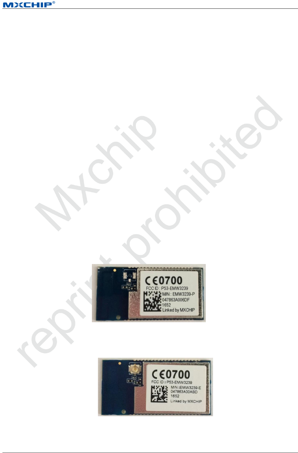
EMW3239Top View
Figure 1.1 Top View of EMW3239-P
Figure 1.2 Top View of EMW3239-E
EMW3239

Application Note [Page 5]
Design Considerations of EMW3239
Module type Antenna type Illustration Manufacture
EMW3239-P On-board PCB
Antenna Default
Dongguan Aosiya
Antenna Technology
Co.,Ltd
EMW3239-E IPEX brass pipe
Antenna Optional
Dongguan Aosiya
Antenna Technology
Co.,Ltd
Antenna Parameter
Parameter EMW3239-E EMW3239-P
Antenna Type Brass pipe Antenna PCB Antenna
Frequency 2400-2500(MHz) 2400-2500(MHz)
Impedance 50ohm 50ohm
VSWR <2 <2
Antenna gain 2dBI 2dBI
Radiation pattern Omnidirectional Omnidirectional
Polarization Vertical Vertical
Datasheet [Page 7]
EMW3239
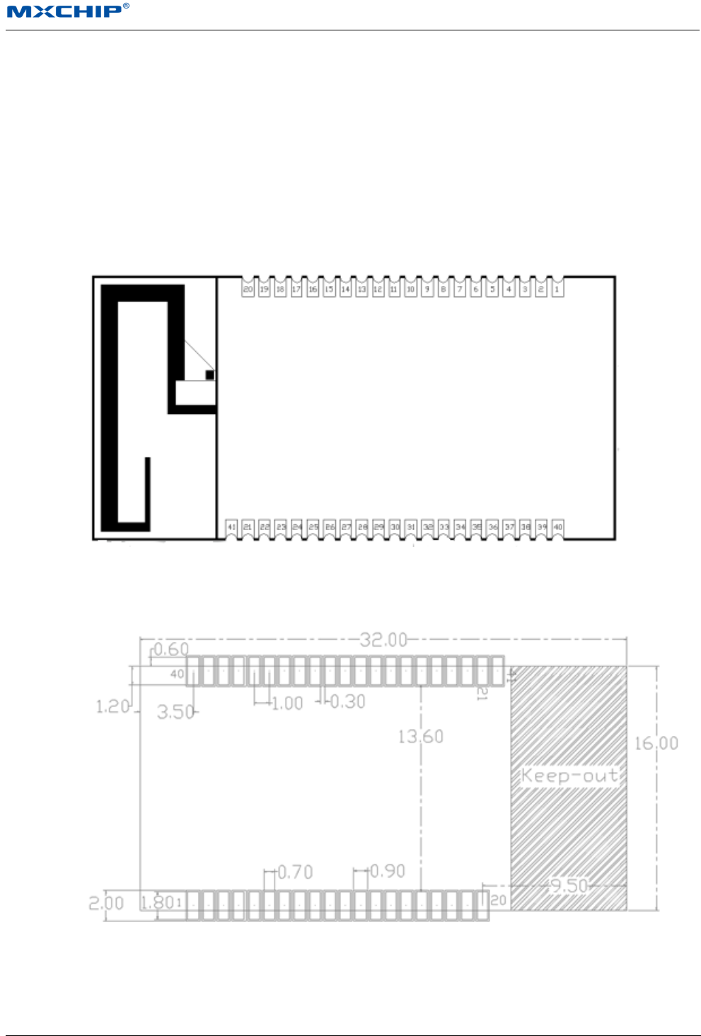
1.1 Pin arrangement
EMW3239 has 41 pins in two rows (1x20 and 1x21) with 0.8mm pitch. Stamp hole package interface design
is used in EMW3239 (as shown in figure 3) to simplify debugging and disassembling for developers, as well as
offering varied selection. Also it is benefit for SMT patch and hand-welding.
Solder mask openness has the same size with land. The width of steel mesh is suggested to be 0.12mm to
0.14mm in SMT.
Figure 4 Pin Arrangement
Figure 5 Package Size of EMW3239
Datasheet [Page 9]
EMW3239
1.2 Pin Definition
1.2.1 EMW3239 Pin Definition
Pins Name Type I/O
Level Multi-select Function User
1 - - - NC
2 PB2 I/O FT GPIO BOOT1 √
3 - - - NC
4 PB15 I/O FT SPI2_MOSI GPIO TIM12_CH2 I2S2_SD √
5 PB12 I/O FT SPI2_NSS GPIO CAN2_RX I2S2_WS √
Table 1 Pin Definition of EMW3239

Datasheet [Page 10]
EMW3239
Pins
Name
Type
I/O
Level
Multi-select Function
User
6
PB13
I/O
FT
SPI2_SCK
GPIO
CAN2_TX
I2S2_CK
√
7
PB14
I/O
FT
SPI2_MISO
GPIO
TIM12_CH1
√
8
PC6
I/O
FT
UART6_TXD
GPIO
TIM3_CH1
I2S2_MCK
×DEBUG_OUT
(
Unusable
)
9
PA15
I/O
FT
GPIO
JTDI
TIM2_CH1
USART1_TXD
×(EasyLink)
10
VBAT
S
-
VBAT
×
11
-
-
-
NC
12
PC7
I/O
FT
UART6_RXD
GPIO
TIM3_CH2
I2S2_CK
×DEBUG_IN
(
Unusable
)
13
NRST
I/O
FT
RESET
×
14
PC0
I
TC
GPIO
WAKEUP
√
15
-
-
-
NC
16
PC13
I/O
FT
GPIO
√
17
PB8
I/O
FT
I2C1_SCL
GPIO
TIM4_CH3
CAN1_RX
√
18
PB9
I/O
FT
I2C1_SDA
GPIO
TIM4_CH4
CAN1_TX
√
19
PB10
I/O
FT
GPIO
TIM2_CH3
I2S2_CK
√
20
GND
S
-
GND
×
21
GND
S
-
GND
×

Datasheet [Page 11]
EMW3239
Pins
Name
Type
I/O
Level
Multi-select Function
User
22
-
-
-
NC
23
-
-
-
NC
24
-
-
-
NC
25
PA14
I/O
FT
SWCLK
×
26
PA13
I/O
FT
SWDIO
×
27
PB3
I/O
FT
GPIO
TIM2_CH2
USART1_RXD
√
28
-
-
-
NC
29
PB7
I/O
FT
UART1_RXD
GPIO
TIM4_CH2
I2C1_SDA
√USER_UART_RX
30
PB6
I/O
FT
UART1_TXD
GPIO
TIM4_CH1
I2C1_SCL
√USER_UART_TX
31
PB4
I/O
FT
GPIO
JTRST
TIM3_CH1
√
32
-
-
-
NC
33
PA10
I/O
FT
USB_ID
GPIO
TIM1_CH3
√
34
PA5
I/O
TC
GPIO
ADC1_5
√
35
PA11
I/O
FT
USB_DM
GPIO
TIM1_CH4
UART1_CTS
√
36
PA12
I/O
FT
USB_DP
GPIO
TIM1_ETR
UART1_RTS
×(BOOT)
37
PB0
I/O
FT
GPIO
ADC1_8
×(STATUS)
38
PA4
I/O
TC
GPIO
ADC1_4
√
39
VDD
S
-
3.3V
×
40
VDD
S
-
3.3V
×
41
ANT
-
-
ANT
×

Datasheet [Page 12]
EMW3239
Illustration:
1. Pin 10, pin 39 and pin 40 should be connected to VDD 3V3, pin 20 and pin 21 should be connected to ground;
2. Pin 8 and pin 12 could only be used in secondary write, ATE or QC automatic detection;
3. Pin 29 and pin 30 is used as serial communication in bootloader mode for users;
4. S stands for power supply, I stands for input pins and I/O stands for input and output pins;
5. FT= 5V tolerant, The maximum voltage should be less than VCC when set as analog input/output or clock
oscillation circuit;
6. TC= 3.6V as convention input/output voltage;
7. SWD(pin 25, pin 26) is used to debug and download firmware instead of JTAG;
8. Pins are not available for users with signature “X” while pins with signature “√” is available for users;
9. For other information please contact technical support.
Application Note [Page 6]
Design Considerations of EMW3239
2. Considerations in Hardware Design
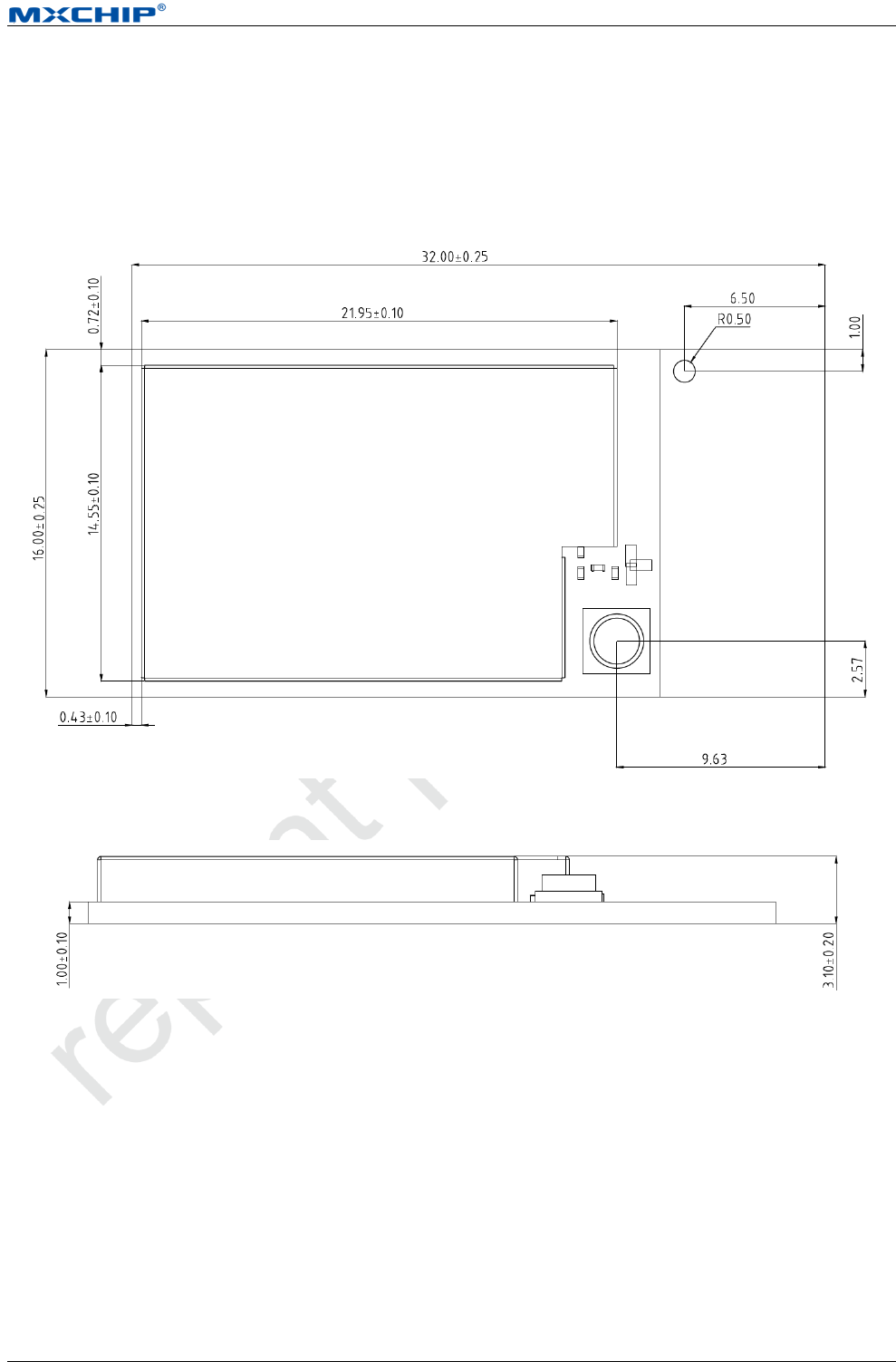
Mechanical Size 2.1
Mechanical size of EMW3031(Unit: mm)
Figure 2.1 Top View of Mechanical Size
Figure 2.2 Side View of Mechanical Size
Reference Package Design 2.2
Solder mask openness has the same size with land, as shown in figure2.3(Unit: mm)
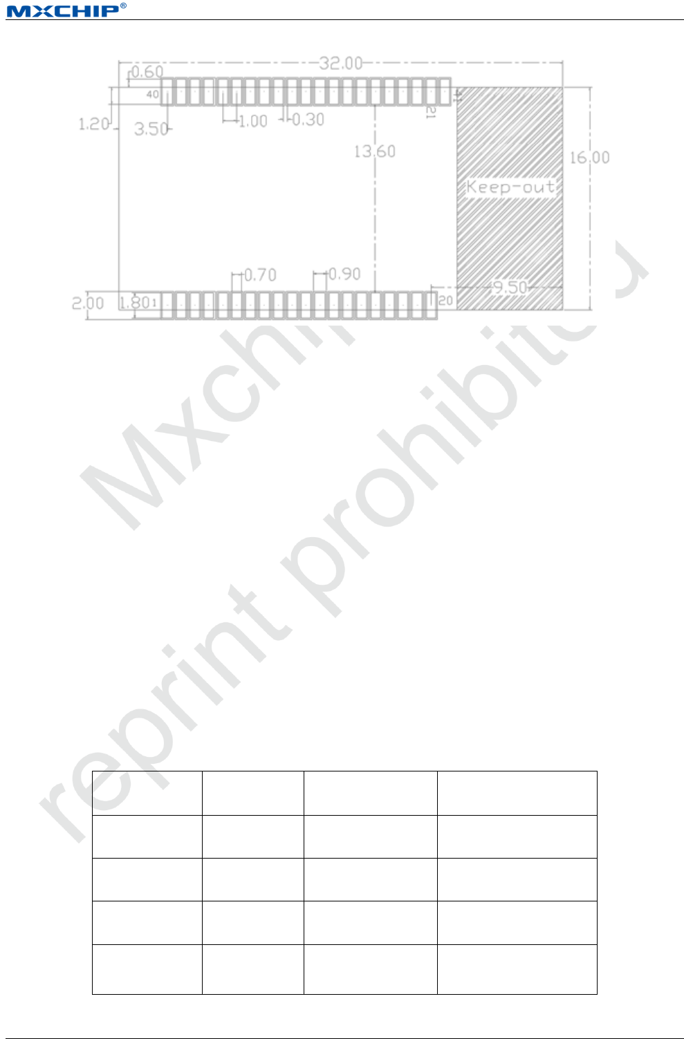
Application Note [Page 7]
Design Considerations of EMW3239
Figure 2.3 SMT Package
DC Power Design 2.3
Peak current of the module is approximately 360mA. DC/DC with maximum output current 600mA is
suggested as power supply. DC/DC is better than LDO in low power consumption.
Route should be particularly aware for DC/DC power supply. Compact element, excellent connection
between input and output ground, long distance between feedback signal and inductance and Schottky diode are
required for route. Details about the requirements should refer to the datasheet of DC/DC device.
Maximum output current and dissipate heat should be aware for the using of LDO. voltage drop is 1.7V when
voltage reduce from 5V to 3.3V. If the current is 300mA, power consumption is1.7V * 360mA=612mW,
PowerDisspation is a parameter on LDO datasheet which should be over 510mW (same methods are used to
calculate other input voltage).
The problem rate about final product would be reduced by fully consideration of power design.
Pin Function 2.4
Set module in different mode by combo PIN 36(BOOT), PIN37(STATUS), PIN9(ELINK).
Table 2.1 Switch Mode
BOOT
STATUS
ELINK
FUNCTION
H
/
/
NORMAL WORK
L
H
L
ATE
L
L
H
QC
L
H
H
BOOTLOADER

Application Note [Page 8]
Design Considerations of EMW3239
Relative contents of the module are sent by pin UART2_TX. Mobile phone could connect to internet and
have normal communication with app at NORMAL WORK. Module must in ATE mode when certificate with
SRRC, FCC, CE. MFG mode could be used in product storage test. Module must in BOOTLOADER mode when
update firmware by UART.
Reset pin
Pin 13 is reset pin triggered by low level voltage. Voltage must over 2.9V. Pin should be in dangling state
when it is not working. There is weak pull-up resistor inside. Please make sure the pin is in high level voltage
when the module is powered on.
SPI
Pin 4~7could be used as off-chip SPI port. Maximum transport rate could be 25Mbps with host and slave
mode, duplex mode and simplex mode.
I2C
Standard mode (100kbps), fast mode (400 kbps), high speed mode (1Mbps) is supported in I2C.
SWDIO/SWCLK
Module supports with one standard SED port without external pull-up or pull-down resistance. Pin 25 and
Pin 26 supports with online debugging and upgrading with J-FLASH or used as GPIO.
GPIO
EMW3239 has 25group of GPIO that could be reused as other pins.
UART
Module has one current control UART communications and one normal UART communication. Pin 29
and Pin 30 are used as serial port of users (Test information, download and communication). Pin 8 and Pin 12
is debugging ports (running log print). Please make sure Wi-Fi RX and TX is connected to host RX and TX.
VBAT
VBAT supports for RTC,PIN10 is clock source which requires power supply 3.3V. External output
compensation calibration in 512HZ could be used in RTC. RTC has programmable alarm and programmable
period interruption wake-up from stop mode to standby mode.
Power supply of EMW3239 is from 2.6V to 3.6V. Low voltage working mode is from 2.6V to 3.0V with
battery. Common working mode is from 3.0V to 3.6V. Rated power is only used as pressure test parameter.
Permanent damage would be caused if the device works in this condition.
Others
Pin floating is not allowed in EMW3239. Pin39 and pin 40 is power supply input that could be added a
10uF ceramic capacitors closing to two pins. Power supply is 2.6V to 3.6V. Module could be breakdown if
the voltage is over 3.6V.
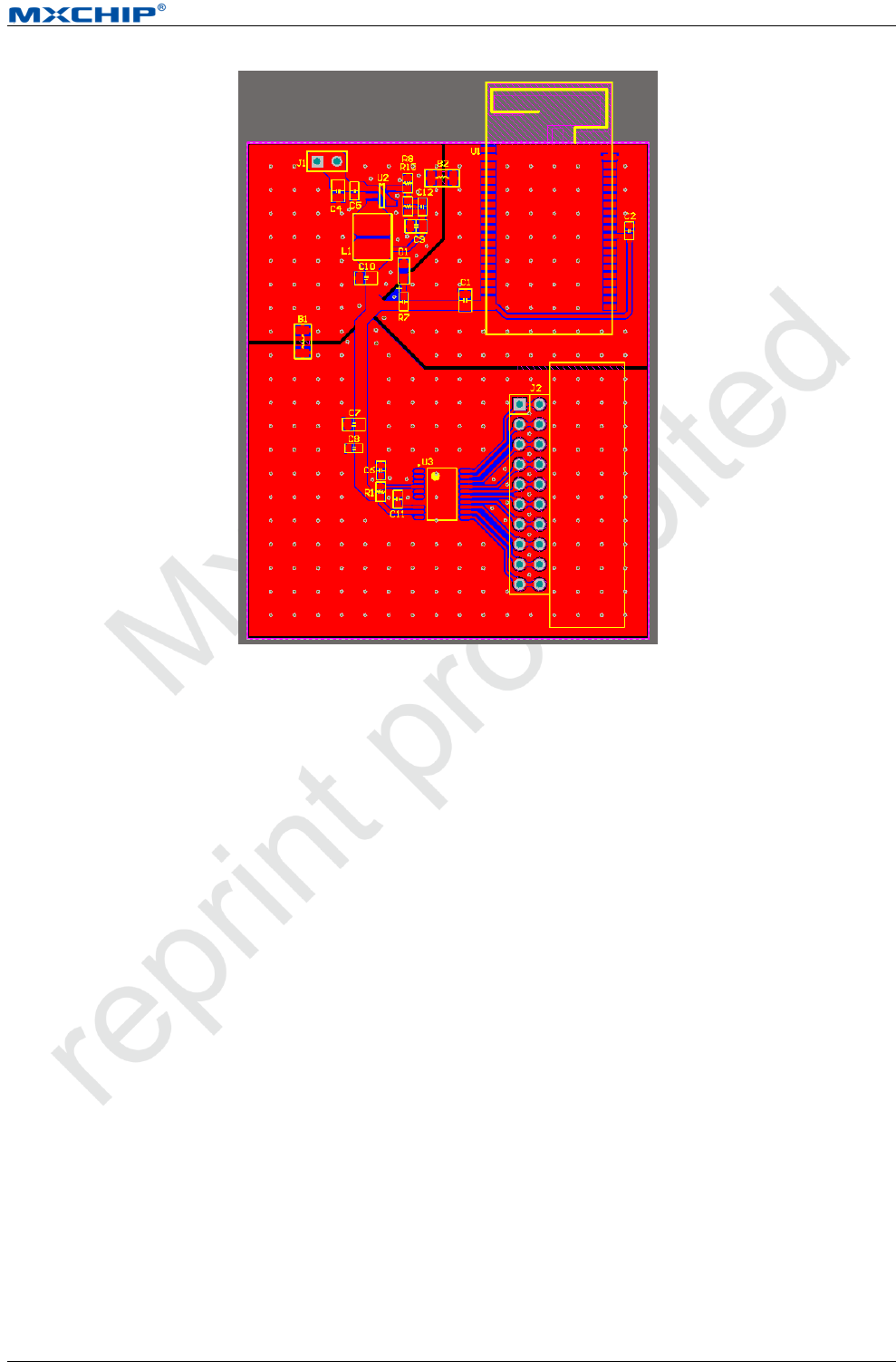
Typical PCB design is shown in figure 2.6.
In order to make sure the antenna performance, sufficient clearance zone should be designed in the
antenna part. PCB part below antenna could be hollowed up. Copper, route, closing to metal element is not
allowed if the structure needed. P1 to P8 should connect to ground with copper.
Application Note [Page 9]
Design Considerations of EMW3239
Figure 2.4 PCB Design
RF Design 2.5
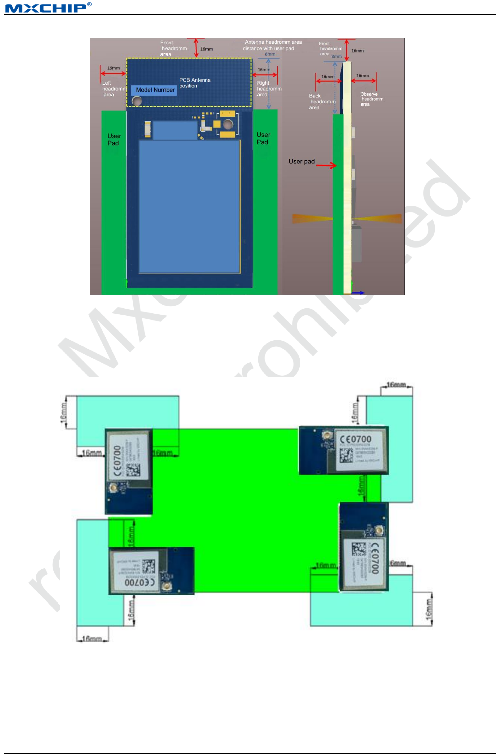
2.5.1 On-board PCB Antenna Design
The main board PCB should be over 16mm far away from other metal components. Copper, route, closing to metal
element is not allowed if the structure needed. P1 to P8 should connect to ground with copper. PCB part below antenna
could be hollowed up.
Application Note [Page 10]
Design Considerations of EMW3239
Figure 2.5 Minimum PCB Clearance Area
In order to reduce the influence from metal components to PCB antenna and wireless signal, it is better to
mount EMW3239 on four parts.
Figure 2.6 Position of the Module
2.5.2 External Antenna
Size of external antenna is shown in figure 2.7. Make sure the correct size with suppliers before buying the
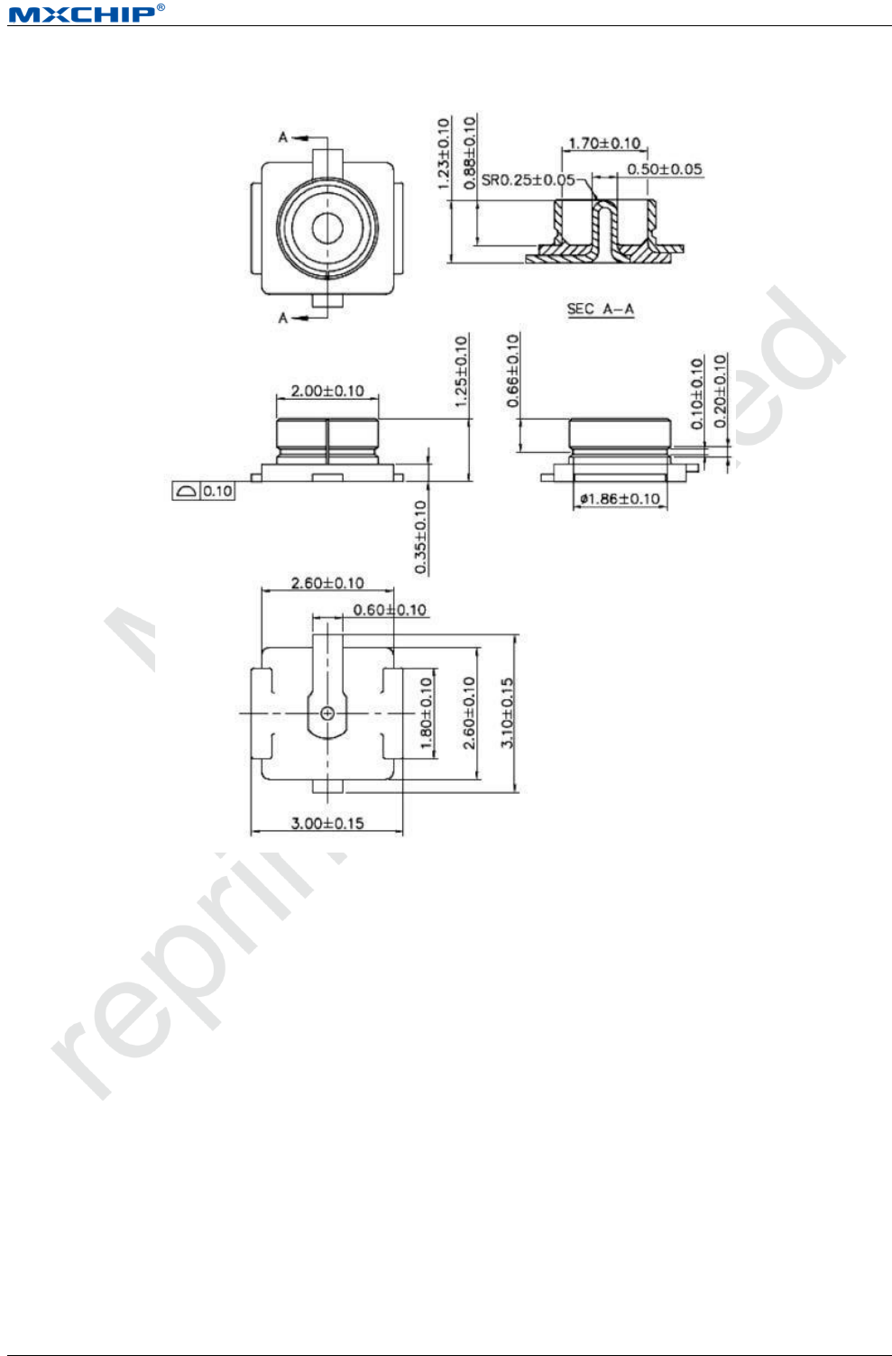
Application Note [Page 11]
Design Considerations of EMW3239
connectors of antenna.
Figure 2.7 Size of External Antenna
ESD Design 2.6
ESD level of the module: Human body model (HBM) is 2000V, charged device model (CDM) is 500V.
Position of ESD protected components should be reserved if the products require higher ESD requirement such as
pins connect to USB and SD-card.
EMI should be aware when the module operated by connecting external wire. Using shielding wire or
reserving common mode choke could avoid EMI.
Application Note [Page 12]
Design Considerations of EMW3239
3. Downloading Firmware and Storage Test Method
Preparations 3.1
Table 3.1Device List
Device
Quantity
PC
1
Tools of downloading firmware
1
EMW3239
1
Micro USB
1
Downloading Software
1
Testing Software
1
Download website is shown in table 3.2.
Table 3.2Download Websites
Name
Function
Websites
FWUpdate
Download
http://pan.baidu.com/s/1kVEwnNh
MicoQcAutoCheck4.0
Test
http://pan.baidu.com/s/1kVEwnNh
CP210x_VCP_Windows
USB Drever
http://www.silabs.com/products/mcu/Pages/SoftwareDownloads.aspx
Firmware program is sent by FAE of MXCHIP or client which is 600K (application code). ‘Test.bin’
is shown in this note.
Switch set up in Downloading Mode 3.2
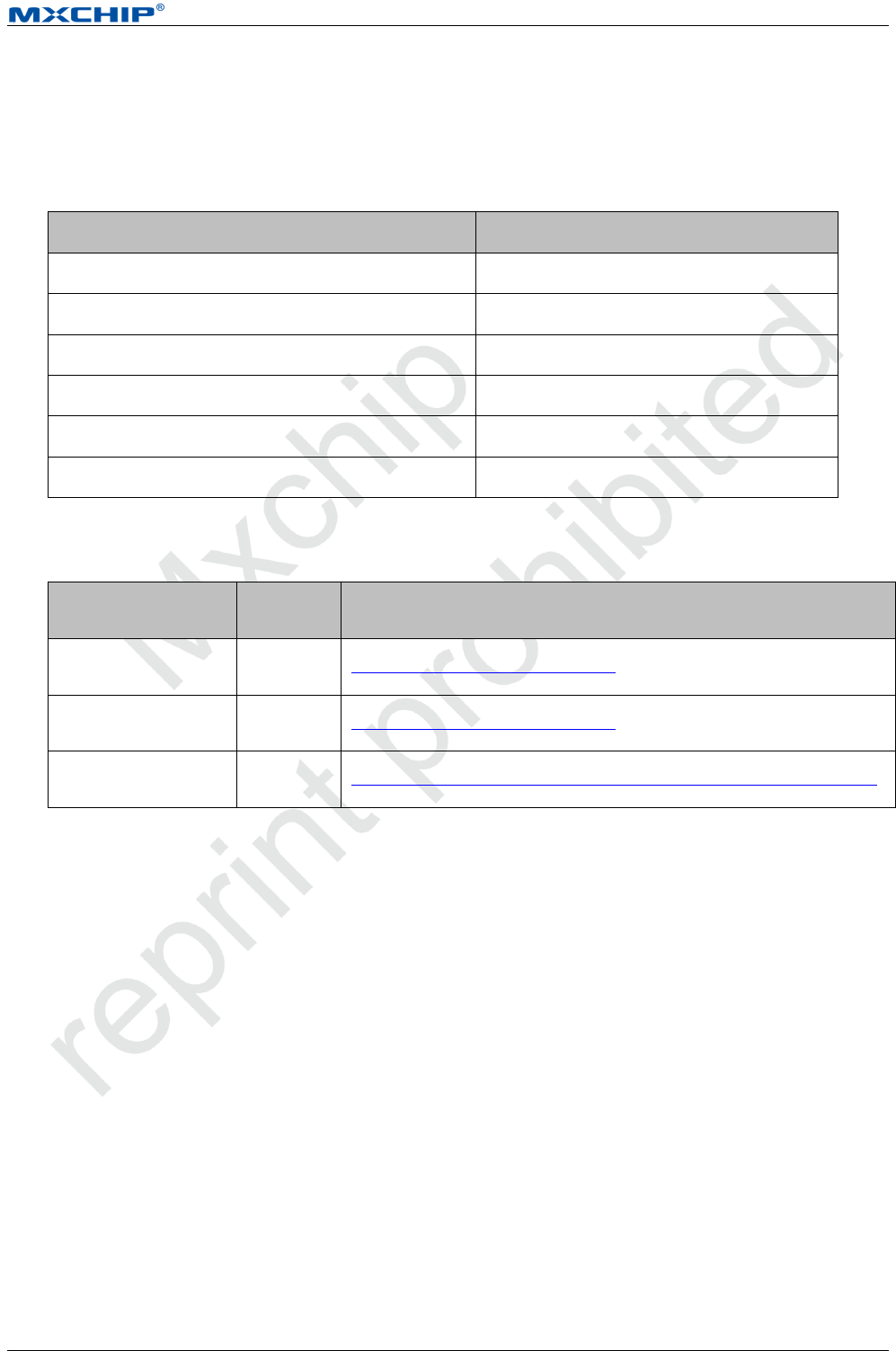
3 switches on develop board of EMW3239 are shown in figure 3.1. Set Easylink as high, STATUS as high
and BOOT as L.
Application Note [Page 13]
Design Considerations of EMW3239
Figure 3.1Switch Set Up
Decompress file ‘CP210X_VCP_WINDOWS.ZIP’. 32 or 64 is based on the computer operating system. It could be checked from
device manager after installing.
System Connection 3.3
Module connects to develop board of EMW3031 with USB. Green light D1 on the develop board enable
when connecting.
Figure 3.2Power Light
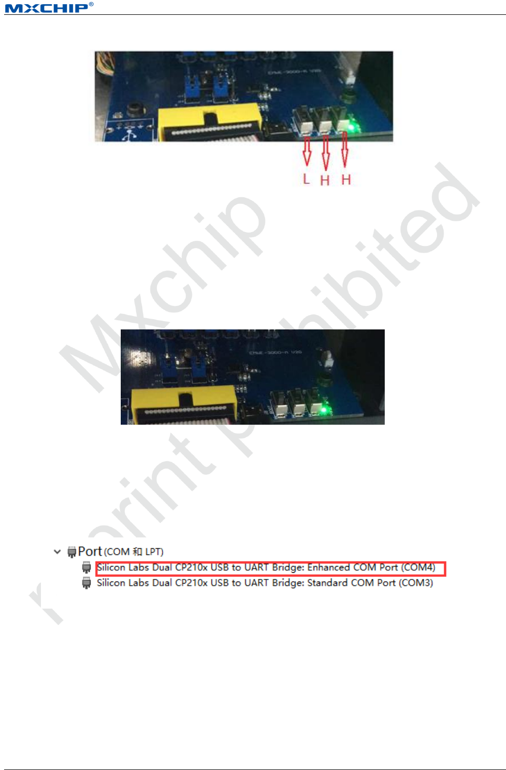
Serial Port Selection 3.4
Find COM number of develop board connect to PC, such as COM4 in figure 3.3. (Note: Enhanced COM Port
must be used in serial number).
Figure 3.3 Name in Device Manager
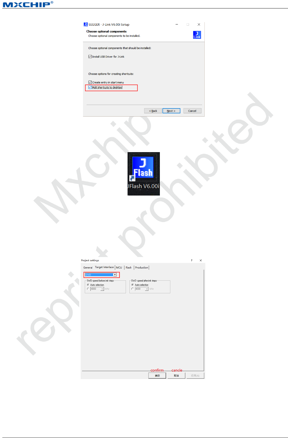
J-Flash 3.5
Install ‘Setup_JLink_V600i.exe’.
Application Note [Page 14]
Design Considerations of EMW3239
Figure 3.4 Install J-Flash
‘JFlash V6.00’ would be found after installing.
Figure 3.5 J-Flash signature
J-Flash Set Up 3.6
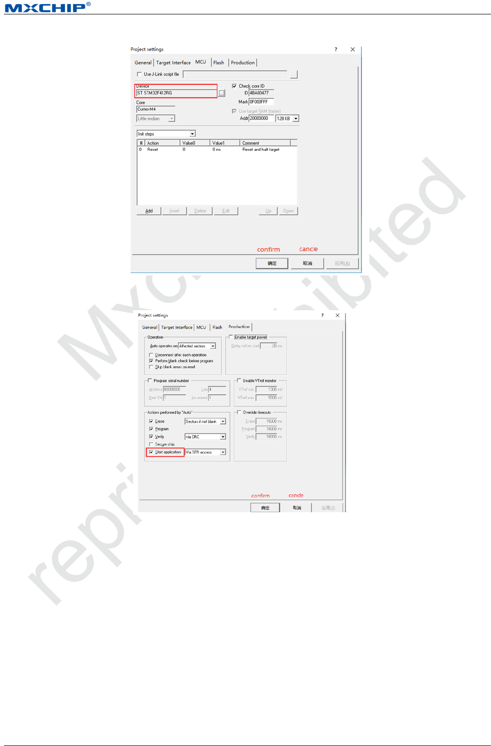
Use ‘ALT+F7’ or open ‘Options’ then click ‘project settings’. Select ‘SWD’ in Target Interface, ‘ST
STM32F412RG’ in MCU, ‘Start application’ in Production.
Figure 3.6 Target Interface Set Up
Application Note [Page 15]
Design Considerations of EMW3239
Figure 3.7 MCU Set Up
Figure 3.8 Production Set Up
Click ‘OK’ after set up. There would be no more set up in following downloading if save the set up.
Testing 3.7
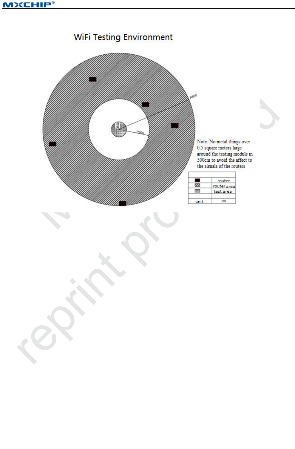
3.7.1 Environment Set Up
Turn on 5 routers that randomly located around test module in a range of 2 to 5 meters.
Application Note [Page 16]
Design Considerations of EMW3239
Figure 3.9 Position of Routers
Important Statement 3.8
MXCHIP has a duty to make sure there is no quality problem when sell the module to customers.
Customers have the rights to ask MXCHIP to exchange goods if the product has quality problem.
If the customer find the problem after welding the module on board without testing at the beginning,
MXCHIP is only responsible for the compensation of the module part.
MXCHIP would help customers solve technical problem in developing firmware without save any MVA/bin
file. Customers should save different development vision and download relative vision in module before
producing.
Application Note [Page 17]
Design Considerations of EMW3239
4. SMT
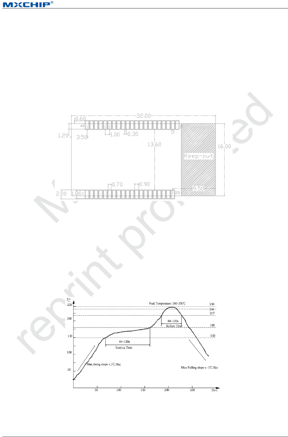
Stencils 4.1
Stencils thickness is suggested as 0.12mm (0.1~0.15mm) with Laser grinding. Recommended solder paste:
No lead SAC305.
Stencils size is shown in figure 4.1, pad holes extend 0.15mm in order to improving solder wicking. If there
is no AOI testing, check module by eye is available to reduce the Pseudo Soldering.
Figure 4.1 Stencils size
Temperature Curve of Secondary Reflow 4.2
Pseudo soldering could be reduced by control the furnace with temperature curve of secondary reflow, as
shown in figure 4.2.
Secondary reflow times less than 2
Peak temperature: 250℃
Figure 4.2 Temperature Curve of Secondary Reflow

Application Note [Page 18]
Design Considerations of EMW3239
5. Mass Production Test and Product Update
Customers should consider not only the function of product but also the testing method in mass production
and update firmware on the product.
Module Test 5.1
In order to avoid inferior module and make sure the correct of downloading firmware, MXCHIP strongly
suggests product testing before produce. Fully test is required after producing.
5.1.1 Half Secondary Development of Firmware
Module connects the MCU from customer through serial port. In secondary development, test command
could be added into firmware. For example, module could scan hotpot around itself and return the results from
serial port by sending testing command through serial port.
5.1.2 Complete Secondary Development of Firmware
Application of customer is based on secondary development of module.
Testing method is variable in complete secondary development mode. Test mode could be set to detect the
performance of the module. The default set up could be used as router for testing. Router is connected when the
module powers on. Details about the test are decided by the application of customers.
Product Update 5.2
OTA is suggested in upgrading the product. OTA is a method to update by wireless.
If the product has bug or inferior, OTA is a better way to update the product.
Send the latest firmware to Cloud. Module would download the firmware into itself when connects to internet.
Latest firmware would be updated after restart automatically.

Application Note [Page 19]
Design Considerations of EMW3239
6. Technical Support
For consultation or purchase the product, please contact Mxchip during working hours:
From Monday to Friday, morning 9:00~12:00, afternoon 13:00~18:00
Telephone: +86-21-52655026
Contact address: 9th Floor, No.5, Lane2145 JinshaJiang Road Putuo District, ShangHai.
Postcode:200333
Email: sales@mxchip.com

Application Note [Page 20]
Design Considerations of EMW3239
7. FCC Statement
When this m odular approved transmitter is integrated into a final host device, and the FCC ID is not visible
from the outside, than the host device must be labeled with an auxiliary label stating
“Contains FCC ID: P53-EMW3239”.
Following statement shall be placed on the final host device:
“This device complies with part 15 of the FCC Rules. Operation is subject to the following two
conditions: (1) This device may not cause harmful interference, and (2) This device must accept any
interference received, including interference that may cause undesired operation.”
When the device is so small or for such use that it is not practicable to place this statement on it, the
statement shall be placed in a prominent location in the instruction manual supplied to the user.
The user manual or instruction manual for an intentional or unintentional radiator shall caution the user
that changes or modifications not expressly approved by the party responsible for compliance could void
the user's authority to operate the equipment.
In addition, Class B digital devices shall have following statement in the user manual:
“NOTE: This equipment has been tested and found to comply with the limits for a Class B digital
device, pursuant to Part 15 of the FCC Rules. These limits are designed to provide reasonable
protection against harmful interference in a residential installation. This equipment generates, uses
and can radiate radio frequency energy and, if not installed and used in accordance with the
instructions, may cause harmful interference to radio communications. However, there is no
guarantee that interference will not occur in a particular installation. If this equipment does cause
harmful interference to radio or television reception, which can be determined by turning the
equipment off and on, the user is encouraged to try to correct the interference by one or more of the
following measures:
-- Reorient or relocate the receiving antenna.
-- Increase the separation between the equipment and receiver.
-- Connect the equipment into an outlet on a circuit different from that to which the receiver is connected.
-- Consult the dealer or an experienced radio/TV technician for help.”
Important Notes:
After integrating this modular approved transmitter according to these instructions in this manual,
following points have to be considered:
- The end-product incl. this modular approved transmitter must comply with the FCC regulations.
The host manufacturer/integrator is required to show compliance with 15B (§15.107 + 15.109) while
the module is installed and operating. In addition, the module should be transmitting and the
evaluation should confirm that the module’s intentional emissions (15 C) are still compliant
(fundamental and out-of-band emission). Verify that there are no additional unintentional emissions
other than what is permitted in 15B or emissions compliant with the transmitter rule. Any additional
non-compliant emissions are unintentional which means that the host is not compliant.
- Additional antennas may be used with this modular approved transmitter, provided they are from
same type, have equal or less gain and have identical in- and outband characteristics as the certified
ones. Other antenna types or antennas with higher gain require appropriate equipment authorization.
- Due to its output power the integration is strictly limited into mobile/fixed categorized host devices
and the user manual of the host device has to include appropriate RF exposure information/warning.
- Any modifications made to the module will void the Grant of Certification, this module is limited to
OEM installation only and must not be sold to end-users, end-user has no manual instructions to
remove or install the device, only software or operating procedure shall be placed in the end-user
operating manual of final products.
- This modular approved transmitter is approved for stand-alone configurations only. For
simultaneous transmission with additional transmitters follow the FCC Multi-transmitter policy.