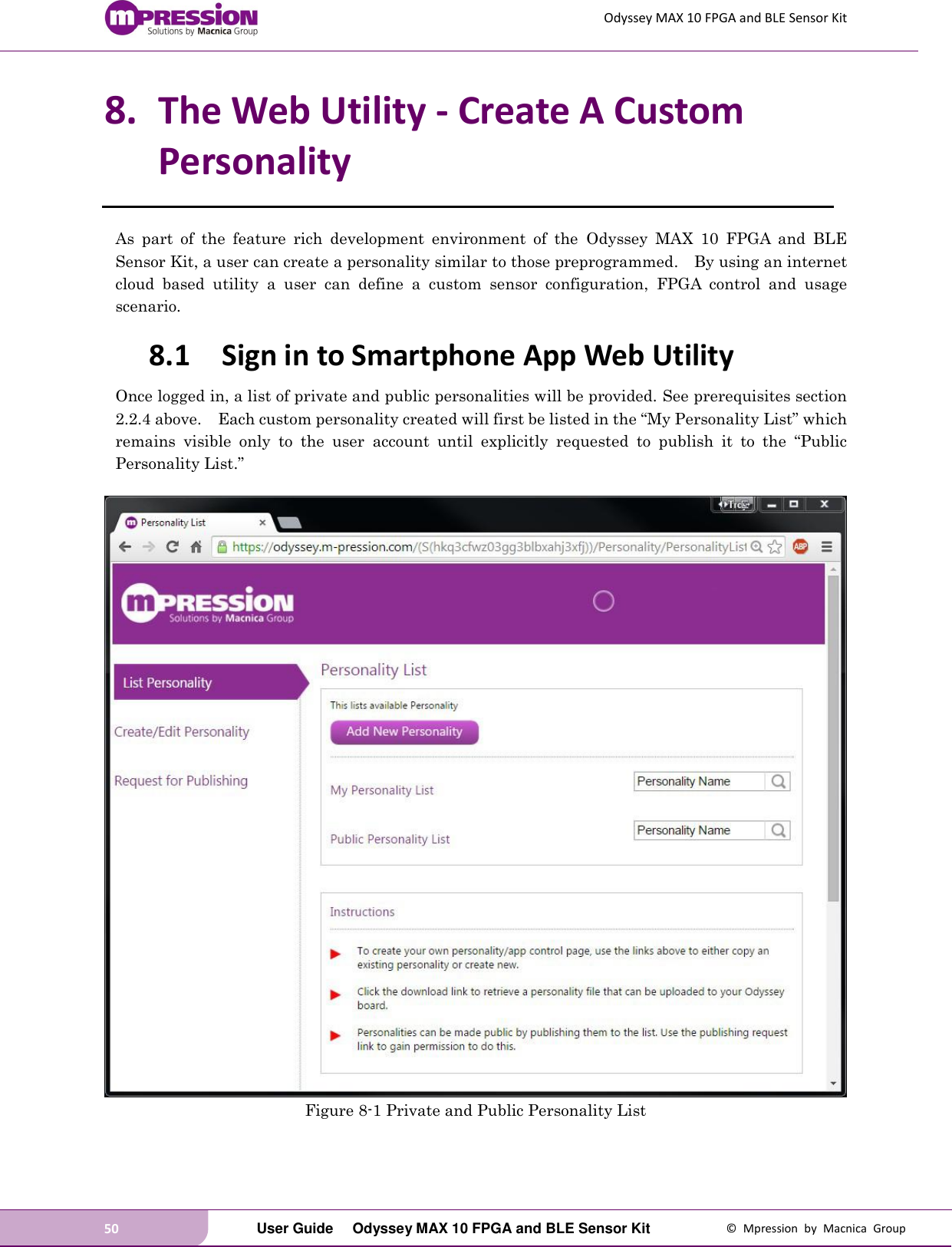
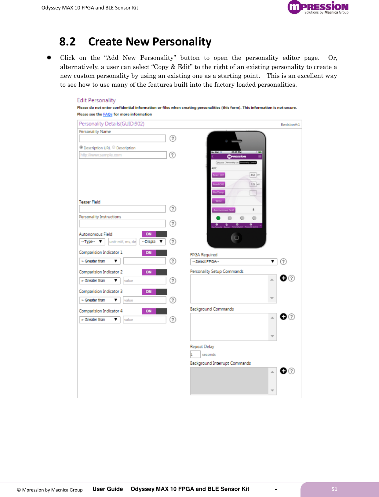
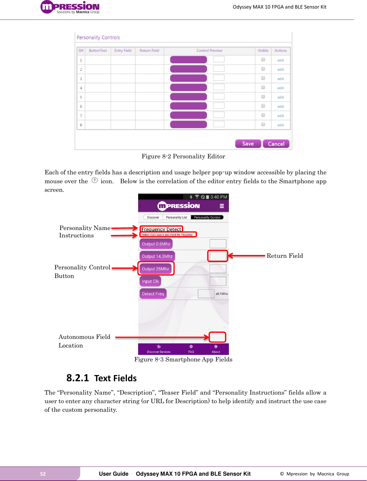
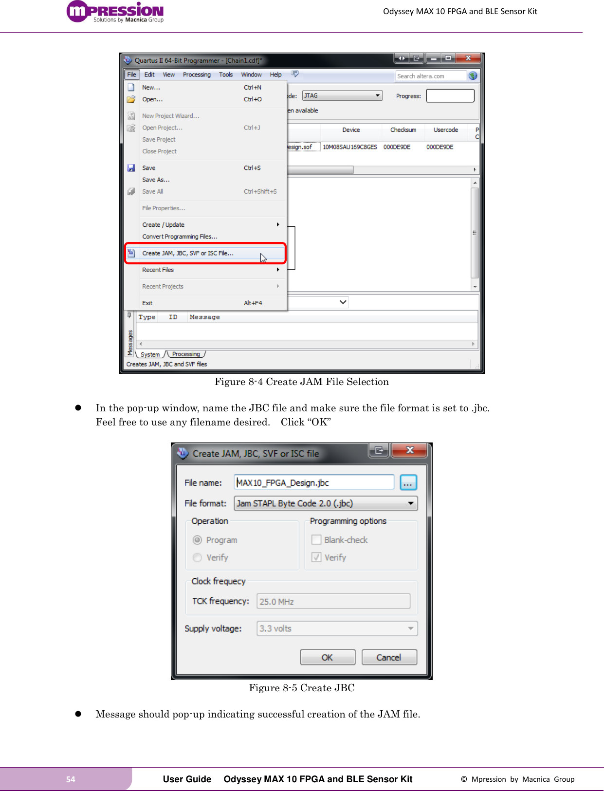
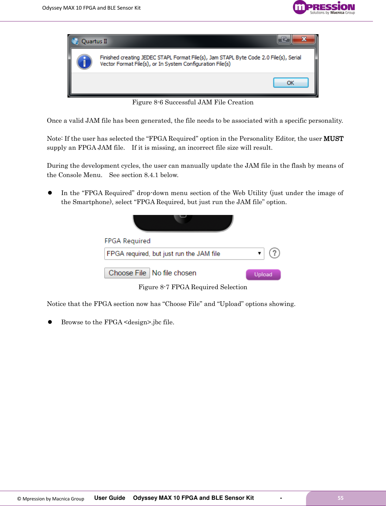
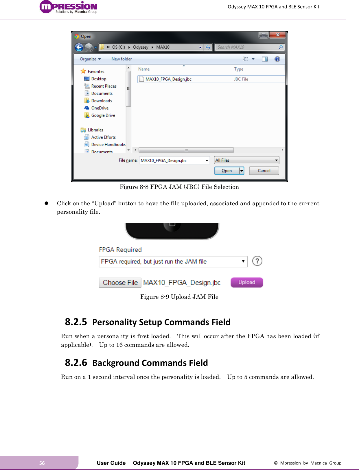
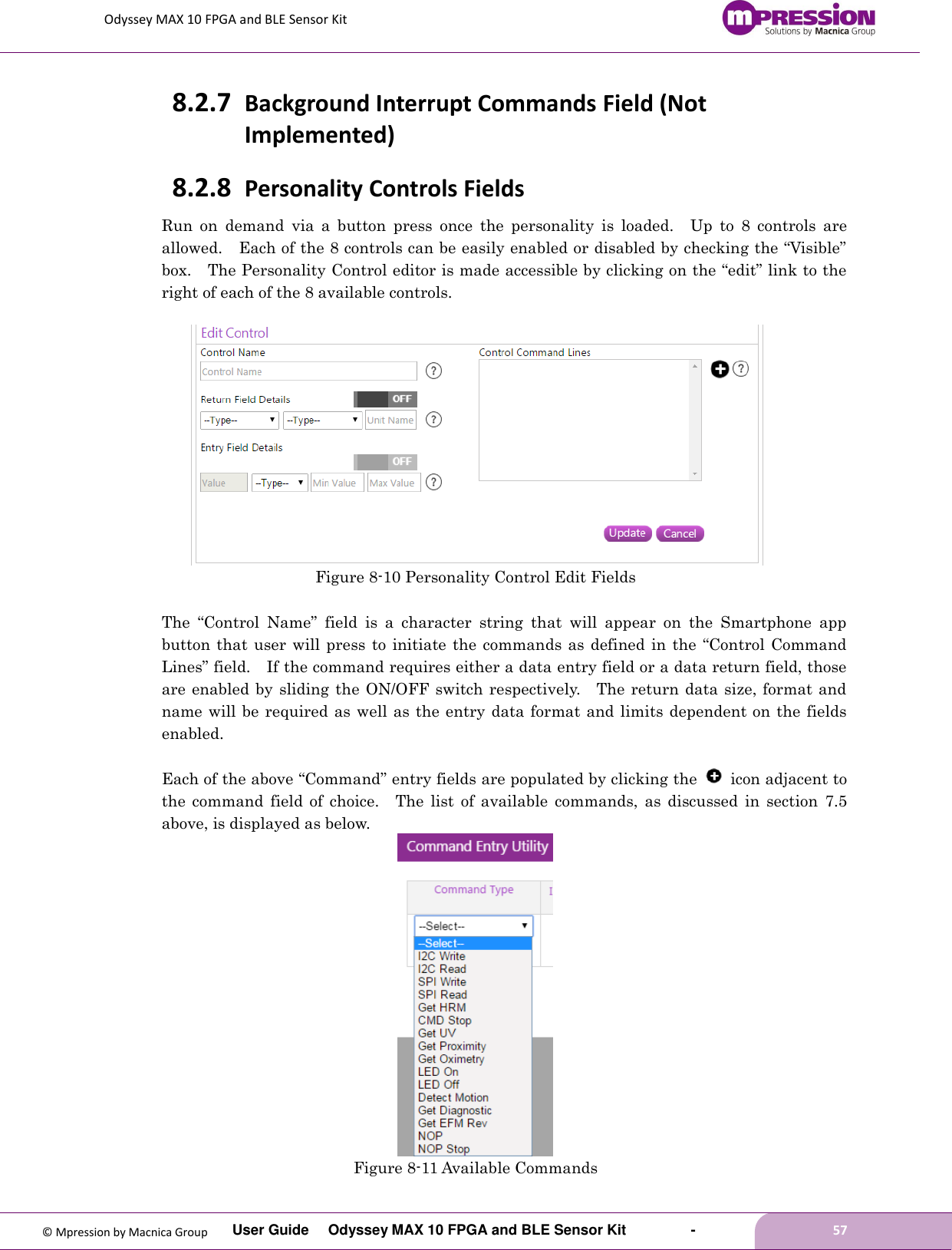
Macnica Americas ODSY001 Sensor Kit with BLE User Manual User Guide
Macnica Americas, Inc. Sensor Kit with BLE User Guide
UserManual.wiki
>
Macnica Americas
>
ODSY001 User Manual
User Manual
Navigation menu
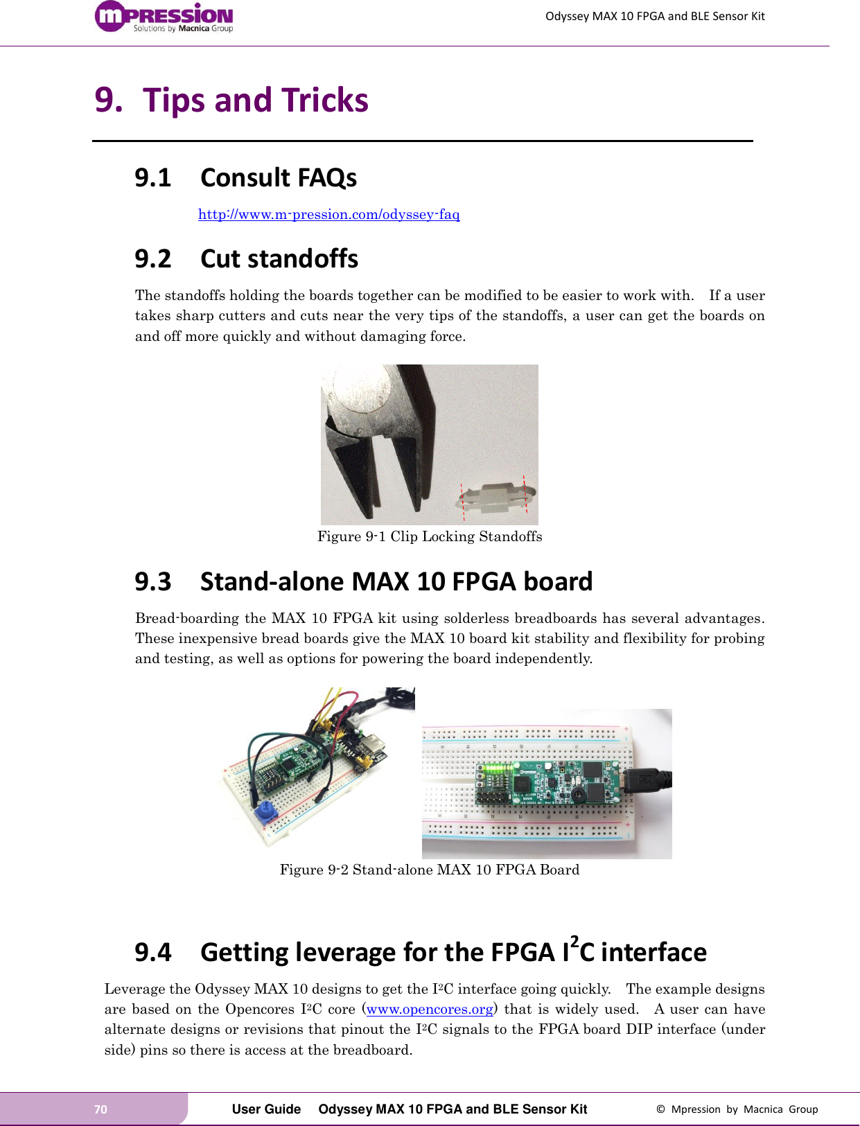
Upload a User Manual
Namespaces
Wiki Guide
HTML
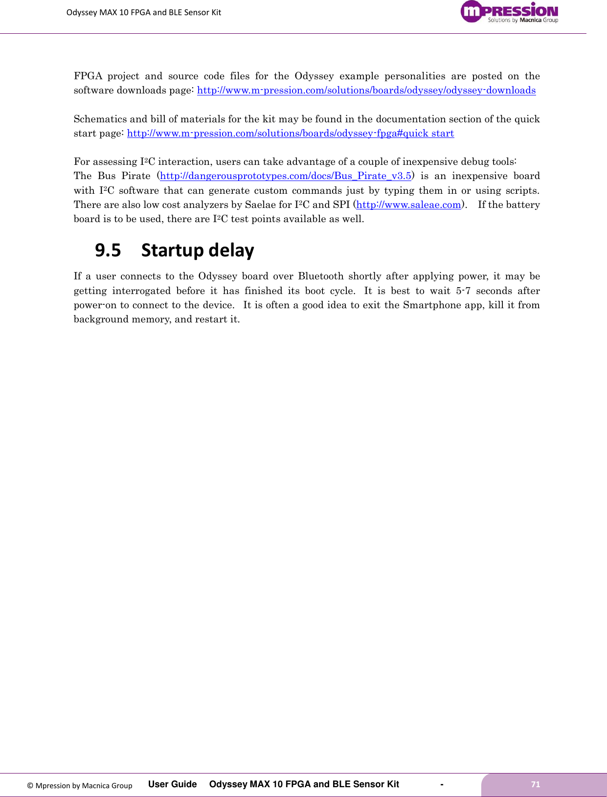
PDF
Info
Views
User Manual
Discussion / Help
Navigation
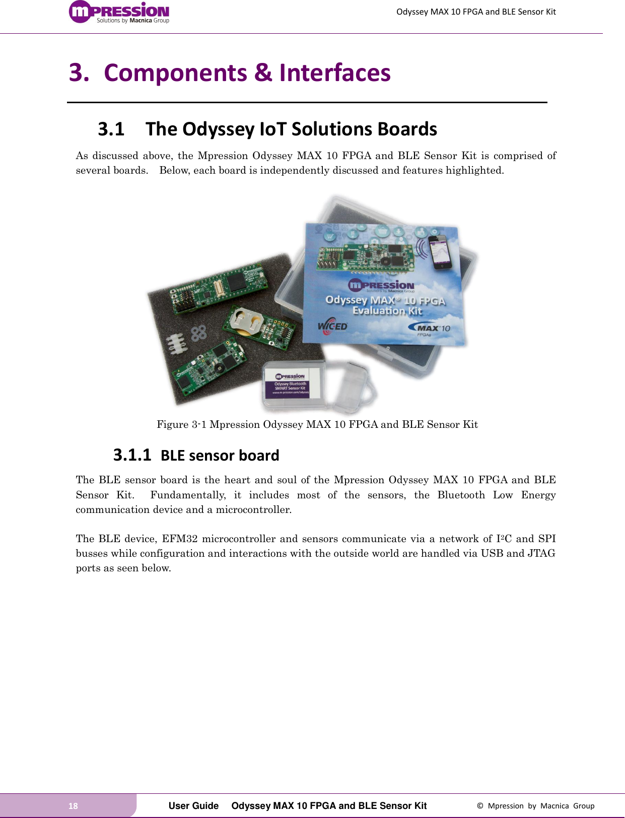
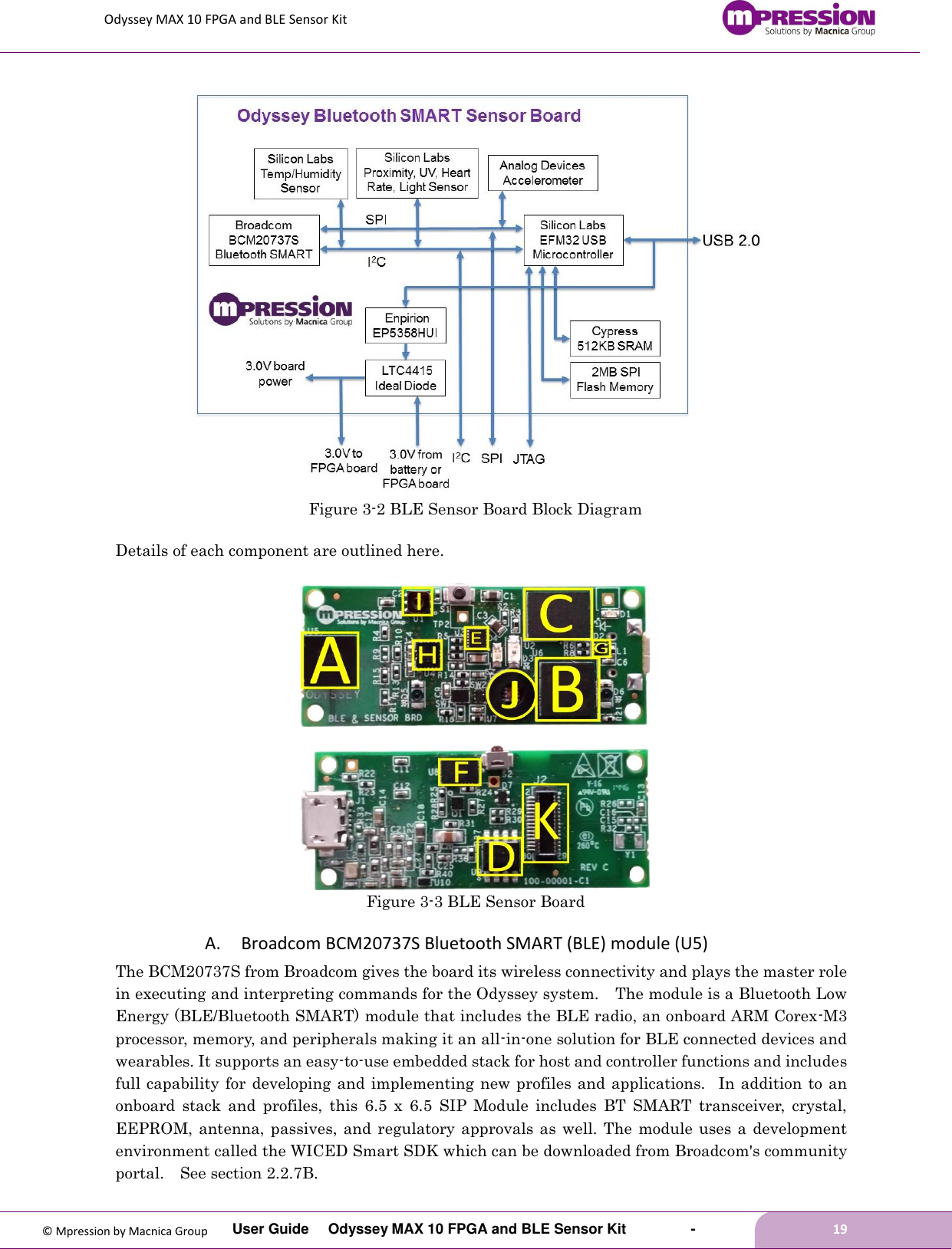
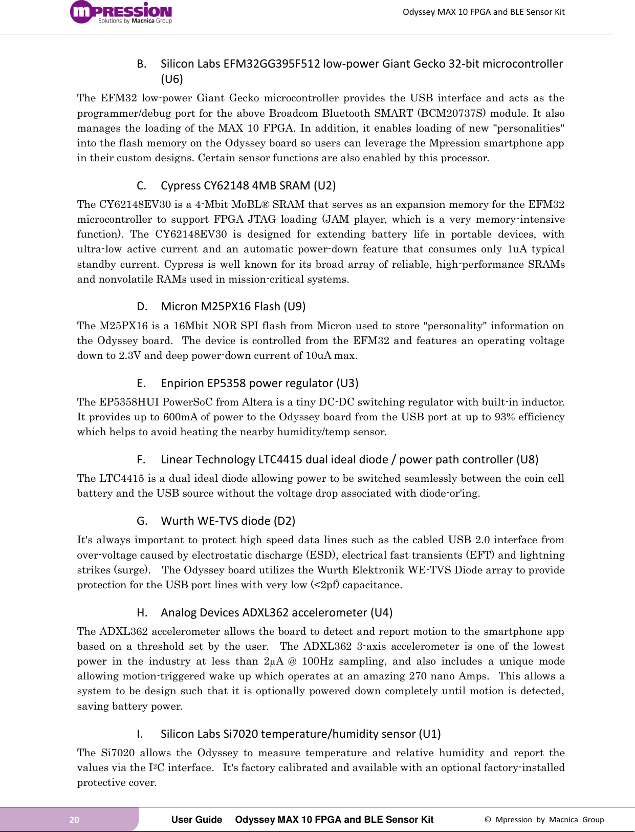
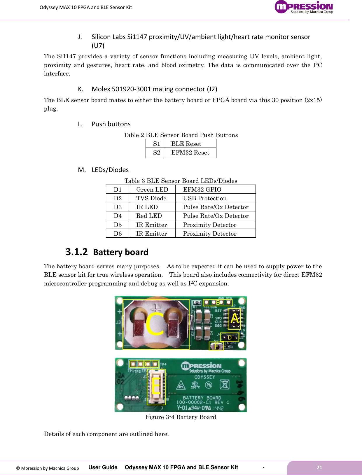
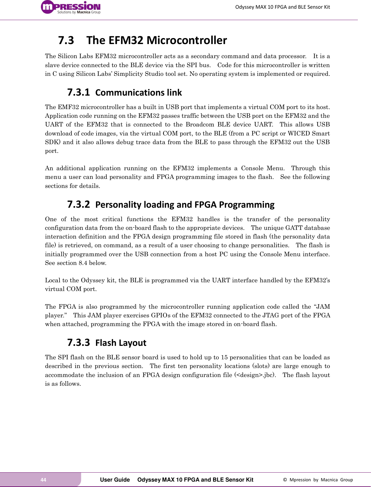
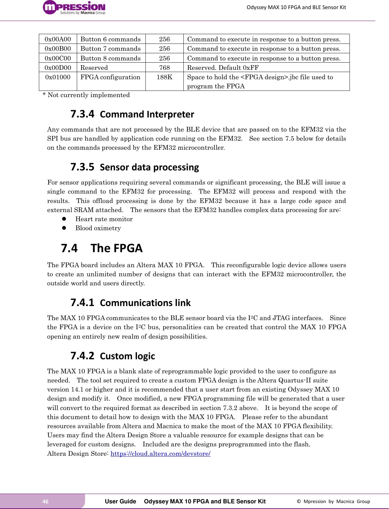
![Odyssey MAX 10 FPGA and BLE Sensor Kit User Guide Odyssey MAX 10 FPGA and BLE Sensor Kit - 45 © Mpression by Macnica Group Table 10: Flash Memory Layout Offset Size (bytes) Description 0x000000 192K Personality 1 data file 0x030000 192K Personality 2 data file 0x060000 192K Personality 3 data file … … … 0x1B0000 192K Personality 10 data file 0x1E0000 8K Personality 11 data file* 0x1E2000 8K Personality 12 data file* … … … 0x1E8000 8K Personality 15 data file* 0x1EA000 88K Reserved *Cannot contain an FPGA design configuration file Each above personality data file entry contains the following information. Table 11: Personality File Format Offset Name Size (bytes) Description 0x00000 Personality number 4 Globally unique number that identifies the personality 0x00004 Personality name 22 Personality name -- Null terminated string 0x0001A FPGA required 1 Bits [1:0] 00: No FPGA required; Erase FPGA 01: FPGA required; Erase and program FPGA 10: No FPGA required; Don’t erase FPGA 11: FPGA required; Don’t erase but program FPGA Bits [7:2] Reserved 0x0001B Revision 1 Personality revision number (optional) 0x0001C Reserved 228 Reserved. Default 0xFF 0x00020 Personality size 4 Size, in bytes, of the Device Personality Flash File. If no FPGA is present, this will be 4096 bytes, otherwise it will vary depending on the FPGA .jbc file size. This file size does not include the checksum byte (if present). 0x00024 Reserved 224 Reserved. Default 0xFF 0x00100 Personality setup commands 512 Commands to execute when the personality is first loaded. Executed by the BLE module after the FPGA is loaded, if applicable. 0x00300 Background commands 256 Commands that execute continuously in the background. 0x00400 Background INT commands 256 Command to execute in response to an interrupt* 0x00500 Button 1 commands 256 Command to execute in response to a button press. 0x00600 Button 2 commands 256 Command to execute in response to a button press. 0x00700 Button 3 commands 256 Command to execute in response to a button press. 0x00800 Button 4 commands 256 Command to execute in response to a button press. 0x00900 Button 5 commands 256 Command to execute in response to a button press.](https://usermanual.wiki/Macnica-Americas/ODSY001/User-Guide-2580488-Page-45.png)