Magnavox Mwc24T5 Service Manual T2202UC
MWC24T5 to the manual 72902cd1-c882-2a24-056f-c117d6b38a4f
2015-01-05
: Magnavox Magnavox-Mwc24T5-Service-Manual-166908 magnavox-mwc24t5-service-manual-166908 magnavox pdf
Open the PDF directly: View PDF ![]() .
.
Page Count: 82
- SPECIFICATIONS
- LASER BEAM SAFETY PRECAUTIONS
- IMPORTANT SAFETY PRECAUTIONS
- STANDARD NOTES FOR SERVICING
- PREPARATION FOR SERVICING
- CABINET DISASSEMBLY INSTRUCTIONS
- ELECTRICAL ADJUSTMENT INSTRUCTIONS
- HOW TO INITIALIZE THE TV/DVD/VCR
- FIRMWARE RENEWAL MODE
- BLOCK DIAGRAMS
- SCHEMATIC DIAGRAMS / CBA’S AND TEST POINTS
- WAVEFORMS
- WIRING DIAGRAM < TV/VCR Section >
- WIRING DIAGRAM < DVD Section >
- SYSTEM CONTROL TIMING CHARTS
- IC PIN FUNCTION DESCRIPTIONS
- LEAD IDENTIFICATIONS
- EXPLODED VIEWS
- MECHANICAL PARTS LIST
- ELECTRICAL PARTS LIST
SERVICE MANUAL
Main Section
I Specifications
I Preparation for Servicing
I Adjustment Procedures
I Schematic Diagrams
I CBA’s
I Exploded Views
I Parts List
When servicing the deck
mechanism, refer to MK14 Deck
Mechanism Section.
Deck Mechanism Part No.:
N2466FT
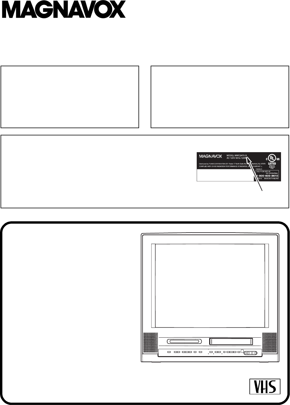
This service manual is for the MWC24T5
version B model, which is different from the
previous model. For MWC24T5 version B
model, a suffix “B” is printed on the rating label
on the back of the unit. Refer to the rating label
illustration at right.
Rating Label
Suffix "B"
24″ COLOR
TV/DVD/VCR
MWC24T5

IMPORTANT SAFETY NOTICE
Proper service and repair is important to the safe, reliable operation of all
Funai Equipment. The service procedures recommended by Funai and
described in this service manual are effective methods of performing
service operations. Some of these service special tools should be used
when and as recommended.
It is important to note that this service manual contains various CAUTIONS
and NOTICES which should be carefully read in order to minimize the risk
of personal injury to service personnel. The possibility exists that improper
service methods may damage the equipment. It also is important to
understand that these CAUTIONS and NOTICES ARE NOT EXHAUSTIVE.
Funai could not possibly know, evaluate and advice the service trade of all
conceivable ways in which service might be done or of the possible
hazardous consequences of each way. Consequently, Funai has not
undertaken any such broad evaluation. Accordingly, a servicer who uses a
service procedure or tool which is not recommended by Funai must first
use all precautions thoroughly so that neither his safety nor the safe
operation of the equipment will be jeopardized by the service method
selected.
Manufactured under license from Dolby Laboratories.
“Dolby” and the double-D symbol are trademarks of Dolby Laboratories.

MAIN SECTION
24″ COLOR TV/DVD/VCR
MWC24T5
TABLE OF CONTENTS
Specifications . . . . . . . . . . . . . . . . . . . . . . . . . . . . . . . . . . . . . . . . . . . . . . . . . . . . . . . . . . . . . . . . . . . . . . . . . .1-1-1
Laser Beam Safety Precautions . . . . . . . . . . . . . . . . . . . . . . . . . . . . . . . . . . . . . . . . . . . . . . . . . . . . . . . . . . . . 1-2-1
Important Safety Precautions . . . . . . . . . . . . . . . . . . . . . . . . . . . . . . . . . . . . . . . . . . . . . . . . . . . . . . . . . . . . . . 1-3-1
Standard Notes for Servicing . . . . . . . . . . . . . . . . . . . . . . . . . . . . . . . . . . . . . . . . . . . . . . . . . . . . . . . . . . . . . .1-4-1
Preparation for Servicing. . . . . . . . . . . . . . . . . . . . . . . . . . . . . . . . . . . . . . . . . . . . . . . . . . . . . . . . . . . . . . . . . .1-5-1
Cabinet Disassembly Instructions. . . . . . . . . . . . . . . . . . . . . . . . . . . . . . . . . . . . . . . . . . . . . . . . . . . . . . . . . . .1-6-1
Electrical Adjustment Instructions . . . . . . . . . . . . . . . . . . . . . . . . . . . . . . . . . . . . . . . . . . . . . . . . . . . . . . . . . . . 1-7-1
How to Initialize the TV/DVD/VCR . . . . . . . . . . . . . . . . . . . . . . . . . . . . . . . . . . . . . . . . . . . . . . . . . . . . . . . . . .1-8-1
Firmware Renewal Mode . . . . . . . . . . . . . . . . . . . . . . . . . . . . . . . . . . . . . . . . . . . . . . . . . . . . . . . . . . . . . . . . .1-9-1
Block Diagrams . . . . . . . . . . . . . . . . . . . . . . . . . . . . . . . . . . . . . . . . . . . . . . . . . . . . . . . . . . . . . . . . . . . . . . . .1-10-1
Schematic Diagrams / CBA’s and Test Points. . . . . . . . . . . . . . . . . . . . . . . . . . . . . . . . . . . . . . . . . . . . . . . . . 1-11-1
Waveforms . . . . . . . . . . . . . . . . . . . . . . . . . . . . . . . . . . . . . . . . . . . . . . . . . . . . . . . . . . . . . . . . . . . . . . . . . . .1-12-1
Wiring Diagram < TV/VCR Section > . . . . . . . . . . . . . . . . . . . . . . . . . . . . . . . . . . . . . . . . . . . . . . . . . . . . . . . 1-13-1
Wiring Diagram < DVD Section > . . . . . . . . . . . . . . . . . . . . . . . . . . . . . . . . . . . . . . . . . . . . . . . . . . . . . . . . . .1-13-2
System Control Timing Charts . . . . . . . . . . . . . . . . . . . . . . . . . . . . . . . . . . . . . . . . . . . . . . . . . . . . . . . . . . . .1-14-1
IC Pin Function Descriptions. . . . . . . . . . . . . . . . . . . . . . . . . . . . . . . . . . . . . . . . . . . . . . . . . . . . . . . . . . . . . .1-15-1
Lead Identifications . . . . . . . . . . . . . . . . . . . . . . . . . . . . . . . . . . . . . . . . . . . . . . . . . . . . . . . . . . . . . . . . . . . . . 1-16-1
Exploded Views. . . . . . . . . . . . . . . . . . . . . . . . . . . . . . . . . . . . . . . . . . . . . . . . . . . . . . . . . . . . . . . . . . . . . . . . 1-17-1
Mechanical Parts List . . . . . . . . . . . . . . . . . . . . . . . . . . . . . . . . . . . . . . . . . . . . . . . . . . . . . . . . . . . . . . . . . . . 1-18-1
Electrical Parts List . . . . . . . . . . . . . . . . . . . . . . . . . . . . . . . . . . . . . . . . . . . . . . . . . . . . . . . . . . . . . . . . . . . . .1-19-1
Main Section
I Specifications
I Preparation for Servicing
I Adjustment Procedures
I Schematic Diagrams
I CBA’s
I Exploded Views
I Parts List

1-1-1 T1200SP
SPECIFICATIONS
*ˆ Mode---------SP mode unless otherwise specified
*Test input terminal
<Except Tuner>--------Video input (1 Vp-p)
Audio input (-10 dB)
<Tuner>------------------Ant. input (80 dBµV) Video: 87.5%
Audio: 25 kHz dev. (1 kHz Sin)
< DEFLECTION >
< VIDEO & CHROMA >
< DVD >
Description Condition Unit Nominal Limit
1. Over Scan --- % 90 5
2. Linearity Horizontal % --- ±18
Ver tical % --- ±10
3. High Voltage --- kV 27 ---
Description Condition Unit Nominal Limit
1. Misconvergence
Center m/m --- 0.4
Corner m/m --- 2.5
Side m/m --- 1.5
2. Tint Control Range --- deg ±30 ---
3. Contrast Control Range --- dB 6 2
4. Brightness (100% White Full Field) Contrast: Max ft-L 40 24
5. Color Temperature --- K 9200 ---
Description Condition Unit Nominal Limit
1. Horizontal Resolution (TDV-540 TIT.2 CHP.16) --- Line 350 300
2. Video S/N at CN3400 (TDV-540 TIT.2 CHP.6) --- dB 60 55
3. S/N Chroma at CN3400
(TDV-540 TIT.2 CHP.17)
AM --- dB 58 53
PM --- dB 58 53
4. Audio Distortion (LPCM 48 kHz, W/LPF)
(PTD 1-NOR TIT.1 CHP.1) L
R% 0.03 0.07
5. Audio freq. response (LPCM 48 kHz)
(PTD 1-NOR TIT.1 CHP.5 -- 10)
L, 20 Hz
R, 20 Hz
L, 20 kHz
R, 20 kHz
dB 0 +4/-5
6. Audio S/N (LPCM 48 kHz,W/LPF,A-WTD)
(PTD 1-NOR TIT.1 CHP.1 -- 2) L
RdB 85 75

1-1-2 T1200SP
< VCR >
< TUNER >
< NORMAL AUDIO>
All items are measured across 8 Ω resistor at speaker output terminal.
< Hi-Fi AUDIO >
Note: Nominal specifications represent the design specifications. All units should be able to approximate these.
Some will exceed and some may drop slightly below these specifications. Limit specifications represent
the absolute worst condition that still might be considered acceptable. In no case should a unit fail to meet
limit specifications.
Description Condition Unit Nominal Limit
1. Horizontal Resolution (R/P, SP) Line 230 200
2. Jitter (Low) (R/P, SP) µs0.10.2
3. S/N Chroma AM(SP) (R/P, SP) dB 38 33
PM(SP) (R/P, SP) dB 38 33
4. Wow & Flutter (JIS, UNWTD) (R/P, SP) % 0.25 0.5
Description Condition Unit Nominal Limit
1. Video S/N (80 dBµV, TV4ch) --- dB 45 40
2. Audio S/N (W/LPF) --- dB 45 40
Description Condition Unit Nominal Limit
1. Audio Output Power (R/P, SP) W 1.0 0.8
2. Audio S/N (W/LPF) (R/P, SP) dB 40 36
3. Audio distortion (W/LPF, -10 dB 1 kHz IN) (R/P, SP) % 3.0 5.0
4. Audio Freq. Response (-10dB 1kHz IN) 200 Hz (R/P, SP) dB -2.0 -2.0±5.0
8 kHz (R/P, SP) dB 0 0±6.0
Description Condition Unit Nominal Limit
1. Output Level (-10 dB 1 kHz IN) (R/P, SP) dB -8.0 -8±4
2. Audio Distortion (-10 dB 1 kHz IN) (R/P, SP) % 0.5 1.0
3. Freq. Response (-15 dB 1 kHz IN) 20 Hz (R/P, SP) dB 0 ±4
20 kHz (R/P, SP) dB 0 ±4
1-2-1 E7NLSP
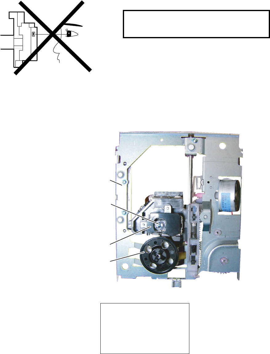
LASER BEAM SAFETY PRECAUTIONS
This DVD player uses a pickup that emits a laser beam.
The laser beam is emitted from the location shown in the figure. When checking the laser diode, be sure to keep
your eyes at least 30 cm away from the pickup lens when the diode is turned on. Do not look directly at the laser
beam.
CAUTION: Use of controls and adjustments, or doing procedures other than those specified herein, may result in
hazardous radiation exposure.
Location: Top of DVD mechanism.
Do not look directly at the laser beam coming
from the pickup or allow it to strike against your
skin.
Drive Mechanism
Assembly
Laser Beam Radiation
Laser Pickup
Turntable
LASER RADIATION
WHEN OPEN. DO NOT
STARE INTO BEAM.
CAUTION
1-3-1 TVDVDN_ISP
IMPORTANT SAFETY PRECAUTIONS
Prior to shipment from the factory, our products are strictly inspected for recognized product safety and electrical
codes of the countries in which they are to be sold. However, in order to maintain such compliance, it is equally
important to implement the following precautions when a set is being serviced.
Safety Precautions for TV Circuit
1. Before returning an instrument to the
customer, always make a safety check of the
entire instrument, including, but not limited to, the
following items:
a. Be sure that no built-in protective devices are
defective and have been defeated during
servicing. (1) Protective shields are provided
on this chassis to protect both the technician
and the customer. Correctly replace all missing
protective shields, including any removed for
servicing convenience. (2) When reinstalling
the chassis and/or other assembly in the
cabinet, be sure to put back in place all
protective devices, including but not limited to,
nonmetallic control knobs, insulating
fishpapers, adjustment and compartment
covers/shields, and isolation resistor/capacitor
networks. Do not operate this instrument or
permit it to be operated without all
protective devices correctly installed and
functioning. Servicers who defeat safety
features or fail to perform safety checks
may be liable for any resulting damage.
b. Be sure that there are no cabinet openings
through which an adult or child might be able to
insert their fingers and contact a hazardous
voltage. Such openings include, but are not
limited to, (1) spacing between the picture tube
and the cabinet mask, (2) excessively wide
cabinet ventilation slots, and (3) an improperly
fitted and/or incorrectly secured cabinet back
cover.
c. Antenna Cold Check - With the instrument AC
plug removed from any AC source, connect an
electrical jumper across the two AC plug
prongs. Place the instrument AC switch in the
on position. Connect one lead of an ohmmeter
to the AC plug prongs tied together and touch
the other ohmmeter lead in turn to each tuner
antenna input exposed terminal screw and, if
applicable, to the coaxial connector. If the
measured resistance is less than 1.0 megohm
or greater than 5.2 megohm, an abnormality
exists that must be corrected before the
instrument is returned to the customer. Repeat
this test with the instrument AC switch in the off
position.
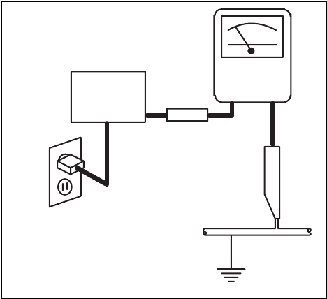
d. Leakage Current Hot Check - With the
instrument completely reassembled, plug the
AC line cord directly into a 120 V AC outlet. (Do
not use an isolation transformer during this
test.) Use a leakage current tester or a
metering system that complies with American
National Standards Institute (ANSI) C101.1
Leakage Current for Appliances and
Underwriters Laboratories (UL) 1410, (50.7).
With the instrument AC switch first in the on
position and then in the off position, measure
from a known earth ground (metal water pipe,
conduit, etc.) to all exposed metal parts of the
instrument (antennas, handle brackets, metal
cabinet, screw heads, metallic overlays, control
shafts, etc.), especially any exposed metal
parts that offer an electrical return path to the
chassis. Any current measured must not
exceed 0.5 milli-ampere. Reverse the
instrument power cord plug in the outlet and
repeat the test.
ANY MEASUREMENTS NOT WITHIN THE
LIMITS SPECIFIED HEREIN INDICATE A
POTENTIAL SHOCK HAZARD THAT MUST
BE ELIMINATED BEFORE RETURNING THE
INSTRUMENT TO THE CUSTOMER OR
BEFORE CONNECTING THE ANTENNA OR
ACCESSORIES.
e. X-Radiation and High Voltage Limits -
Because the picture tube is the primary
potential source of X-radiation in solid-state TV
receivers, it is specially constructed to prohibit
X-radiation emissions. For continued X-
radiation protection, the replacement picture
tube must be the same type as the original.
ALSO TEST WITH
PLUG REVERSED
USING AC
ADAPTER PLUG
AS REQUIRED
TEST ALL EXPOSED
METAL SURFACES
READING SHOULD
NOT BE ABOVE 0.5 mA
EARTH
GROUND
_
DEVICE LEAKAGE
CURRENT
TESTER
+
BEING
TESTED
1-3-2 TVDVDN_ISP
Also, because the picture tube shields and
mounting hardware perform an X-radiation
protection function, they must be correctly in
place. High voltage must be measured each
time servicing is performed that involves B+,
horizontal deflection or high voltage. Correct
operation of the X-radiation protection circuits
also must be reconfirmed each time they are
serviced. (X-radiation protection circuits also
may be called “horizontal disable” or “hold
down.”) Read and apply the high voltage limits
and, if the chassis is so equipped, the X-
radiation protection circuit specifications given
on instrument labels and in the Product Safety
& X-Radiation Warning note on the service
data chassis schematic. High voltage is
maintained within specified limits by close
tolerance safety-related components/
adjustments in the high-voltage circuit. If high
voltage exceeds specified limits, check each
component specified on the chassis schematic
and take corrective action.
2. Read and comply with all caution and safety-
related notes on or inside the receiver cabinet, on
the receiver chassis, or on the picture tube.
3. Design Alteration Warning - Do not alter or add
to the mechanical or electrical design of this TV
receiver. Design alterations and additions,
including, but not limited to circuit modifications
and the addition of items such as auxiliary audio
and/or video output connections, might alter the
safety characteristics of this receiver and create a
hazard to the user. Any design alterations or
additions will void the manufacturer's warranty and
may make you, the servicer, responsible for
personal injury or property damage resulting
therefrom.
4. Picture Tube Implosion Protection Warning -
The picture tube in this receiver employs integral
implosion protection. For continued implosion
protection, replace the picture tube only with one
of the same type number. Do not remove, install,
or otherwise handle the picture tube in any
manner without first putting on shatterproof
goggles equipped with side shields. People not so
equipped must be kept safely away while picture
tubes are handled. Keep the picture tube away
from your body. Do not handle the picture tube by
its neck. Some “in-line” picture tubes are equipped
with a permanently attached deflection yoke;
because of potential hazard, do not try to remove
such “permanently attached” yokes from the
picture tube.
5. Hot Chassis Warning -
a. Some TV receiver chassis are electrically
connected directly to one conductor of the AC
power cord and maybe safety-serviced without
an isolation transformer only if the AC power
plug is inserted so that the chassis is
connected to the ground side of the AC power
source. To confirm that the AC power plug is
inserted correctly, with an AC voltmeter,
measure between the chassis and a known
earth ground. If a voltage reading in excess of
1.0V is obtained, remove and reinsert the AC
power plug in the opposite polarity and again
measure the voltage potential between the
chassis and a known earth ground.
b. Some TV receiver chassis normally have 85V
AC(RMS) between chassis and earth ground
regardless of the AC plug polarity. This chassis
can be safety-serviced only with an isolation
transformer inserted in the power line between
the receiver and the AC power source, for both
personnel and test equipment protection.
c. Some TV receiver chassis have a secondary
ground system in addition to the main chassis
ground. This secondary ground system is not
isolated from the AC power line. The two
ground systems are electrically separated by
insulation material that must not be defeated or
altered.
6. Observe original lead dress. Take extra care to
assure correct lead dress in the following areas: a.
near sharp edges, b. near thermally hot parts-be
sure that leads and components do not touch
thermally hot parts, c. the AC supply, d. high
voltage, and, e. antenna wiring. Always inspect in
all areas for pinched, out of place, or frayed wiring.
Check AC power cord for damage.
7. Components, parts, and/or wiring that appear to
have overheated or are otherwise damaged
should be replaced with components, parts, or
wiring that meet original specifications.
Additionally, determine the cause of overheating
and/or damage and, if necessary, take corrective
action to remove any potential safety hazard.
8. Product Safety Notice - Some electrical and
mechanical parts have special safety-related
characteristics which are often not evident from
visual inspection, nor can the protection they give
necessarily be obtained by replacing them with
components rated for higher voltage, wattage, etc.
Parts that have special safety characteristics are
identified by a # on schematics and in parts lists.
Use of a substitute replacement that does not
have the same safety characteristics as the
recommended replacement part might create
shock, fire, and/or other hazards. The product's
safety is under review continuously and new
instructions are issued whenever appropriate.
Prior to shipment from the factory, our products
are strictly inspected to confirm they comply with
the recognized product safety and electrical codes
1-3-3 TVDVDN_ISP
of the countries in which they are to be sold.
However, in order to maintain such compliance, it
is equally important to implement the following
precautions when a set is being serviced.
Precautions during Servicing
A. Parts identified by the # symbol are critical for
safety.
Replace only with part number specified.
B. In addition to safety, other parts and assemblies
are specified for conformance with regulations
applying to spurious radiation. These must also be
replaced only with specified replacements.
Examples: RF converters, RF cables, noise
blocking capacitors, and noise blocking filters, etc.
C. Use specified internal wiring. Note especially:
1) Wires covered with PVC tubing
2) Double insulated wires
3) High voltage leads
D. Use specified insulating materials for hazardous
live parts. Note especially:
1) Insulation Tape
2) PVC tubing
3) Spacers
4) Insulators for transistors.
E. When replacing AC primary side components
(transformers, power cord, etc.), wrap ends of
wires securely about the terminals before
soldering.
F. Observe that the wires do not contact heat
producing parts (heat sinks, oxide metal film
resistors, fusible resistors, etc.)
G. Check that replaced wires do not contact sharp
edged or pointed parts.
H. When a power cord has been replaced, check that
5~6 kg of force in any direction will not loosen it.
I. Also check areas surrounding repaired locations.
J. Be careful that foreign objects (screws, solder
droplets, etc.) do not remain inside the set.
K. Crimp type wire connector
When replacing the power transformer in sets
where the connections between the power cord
and power transformer primary lead wires are
performed using crimp type connectors, in order to
prevent shock hazards, perform carefully and
precisely the following steps.
Replacement procedure
1) Remove the old connector by cutting the wires
at a point close to the connector.
Important: Do not re-use a connector (discard
it).
2) Strip about 15 mm of the insulation from the
ends of the wires. If the wires are stranded,
twist the strands to avoid frayed conductors.
3) Align the lengths of the wires to be connected.
Insert the wires fully into the connector.
4) Use the crimping tool to crimp the metal sleeve
at the center position. Be sure to crimp fully to
the complete closure of the tool.
L. When connecting or disconnecting the DVD/VCR
connectors, first, disconnect the AC plug from the
AC supply socket.
1-3-4 TVDVDN_ISP
Safety Check after Servicing
Examine the area surrounding the repaired location for damage or deterioration. Observe that screws, parts and
wires have been returned to original positions. Afterwards, perform the following tests and confirm the specified
values in order to verify compliance with safety standards.
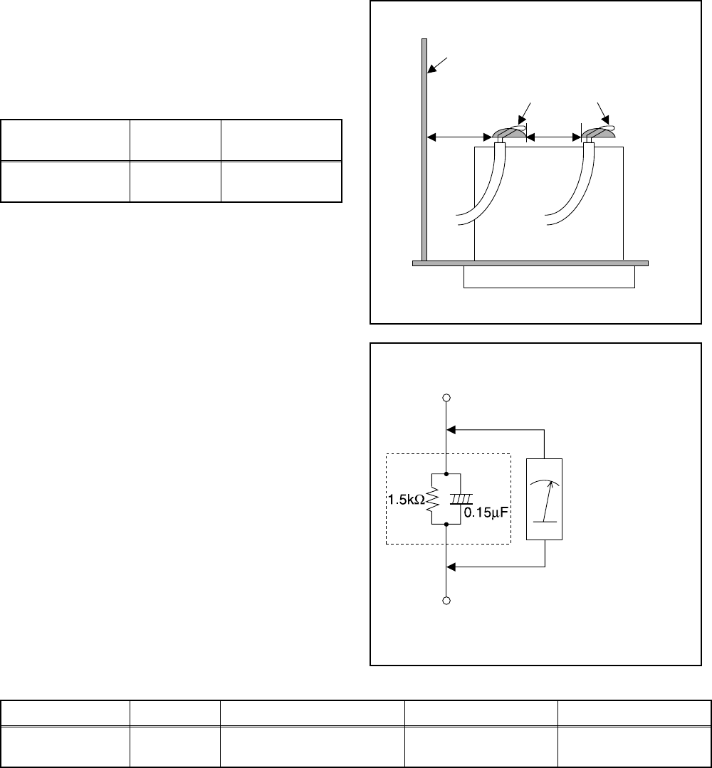
1. Clearance Distance
When replacing primary circuit components, confirm
specified clearance distance (d) and (d') between
soldered terminals, and between terminals and
surrounding metallic parts. (See Fig. 1)
Table 1: Ratings for selected area
Note: This table is unofficial and for reference only. Be
sure to confirm the precise values.
2. Leakage Current Test
Confirm the specified (or lower) leakage current
between B (earth ground, power cord plug prongs) and
externally exposed accessible parts (RF terminals,
antenna terminals, video and audio input and output
terminals, microphone jacks, earphone jacks, etc.).
Measuring Method: (Power ON)
Insert load Z between B (earth ground, power cord plug
prongs) and exposed accessible parts. Use an AC
voltmeter to measure across both terminals of load Z.
See Fig. 2 and following table.
Table 2: Leakage current ratings for selected areas
Note: This table is unofficial and for reference only. Be sure to confirm the precise values.
AC Line Voltage Region Clearance
Distance (d), (d’)
110 to 130 V U.S.A. or
Canada ≥ 3.2 mm
(0.126 inches)
AC Line Voltage Region Load Z Leakage Current (i) Earth Ground (B) to:
110 to 130 V U.S.A. or
Canada 0.15 µF CAP. & 1.5 kΩ
RES. Connected in parallel i ≤ 0.5 mA rms Exposed accessible
parts
Chassis or Secondary Conductor
Primary Circuit
Fig. 1
d' d
AC Voltmeter
(High Impedance)
Exposed Accessible Part
BEarth Ground
Power Cord Plug Prongs
Z
Fig. 2
1-4-1 TVDVDN_SN
STANDARD NOTES FOR SERVICING
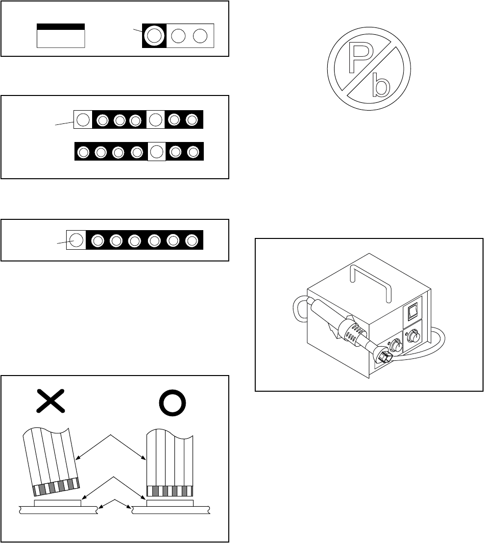
Circuit Board Indications
1. The output pin of the 3 pin Regulator ICs is
indicated as shown.
2. For other ICs, pin 1 and every fifth pin are
indicated as shown.
3. The 1st pin of every male connector is indicated as
shown.
Instructions for Connectors
1. When you connect or disconnect the FFC (Flexible
Foil Connector) cable, be sure to first disconnect
the AC cord.
2. FFC (Flexible Foil Connector) cable should be
inserted parallel into the connector, not at an
angle.
Pb (Lead) Free Solder
Pb free mark will be found on PCBs which use Pb
free solder. (Refer to figure.) For PCBs with Pb free
mark, be sure to use Pb free solder. For PCBs
without Pb free mark, use standard solder.
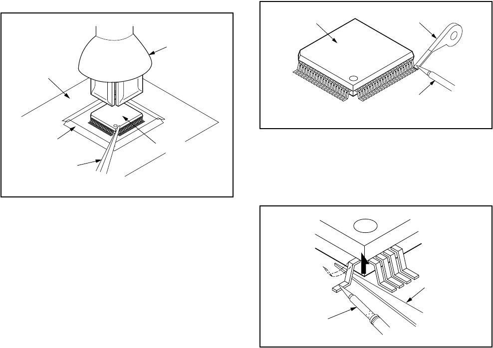
How to Remove / Install Flat Pack-IC
1. Removal
With Hot-Air Flat Pack-IC Desoldering Machine:
1. Prepare the hot-air flat pack-IC desoldering
machine, then apply hot air to the Flat Pack-IC
(about 5 to 6 seconds). (Fig. S-1-1)
2. Remove the flat pack-IC with tweezers while
applying the hot air.
3. Bottom of the flat pack-IC is fixed with glue to the
CBA; when removing entire flat pack-IC, first apply
soldering iron to center of the flat pack-IC and heat
up. Then remove (glue will be melted). (Fig. S-1-6)
4. Release the flat pack-IC from the CBA using
tweezers. (Fig. S-1-6)
CAUTION:
1. The Flat Pack-IC shape may differ by models. Use
an appropriate hot-air flat pack-IC desoldering
machine, whose shape matches that of the Flat
Pack-IC.
2. Do not supply hot air to the chip parts around the
flat pack-IC for over 6 seconds because damage
to the chip parts may occur. Put masking tape
Top View
Out In
Bottom View
Input
5
10
Pin 1
Pin 1
FFC Cable
Connector
CBA
* Be careful to avoid a short circuit.
Pb free mark
Fig. S-1-1
1-4-2 TVDVDN_SN
around the flat pack-IC to protect other parts from
damage. (Fig. S-1-2)
3. The flat pack-IC on the CBA is affixed with glue, so
be careful not to break or damage the foil of each
pin or the solder lands under the IC when
removing it.
With Soldering Iron:
1. Using desoldering braid, remove the solder from
all pins of the flat pack-IC. When you use solder
flux which is applied to all pins of the flat pack-IC,
you can remove it easily. (Fig. S-1-3)
2. Lift each lead of the flat pack-IC upward one by
one, using a sharp pin or wire to which solder will
not adhere (iron wire). When heating the pins, use
a fine tip soldering iron or a hot air desoldering
machine. (Fig. S-1-4)
3. Bottom of the flat pack-IC is fixed with glue to the
CBA; when removing entire flat pack-IC, first apply
soldering iron to center of the flat pack-IC and heat
up. Then remove (glue will be melted). (Fig. S-1-6)
4. Release the flat pack-IC from the CBA using
tweezers. (Fig. S-1-6)
Hot-air
Flat Pack-IC
Desoldering
Machine
CBA
Flat Pack-IC
Tweezers
Masking
Tape
Fig. S-1-2
Flat Pack-IC Desoldering Braid
Soldering Iron
Fig. S-1-3
Fine Tip
Soldering Iron
Sharp
Pin
Fig. S-1-4
1-4-3 TVDVDN_SN
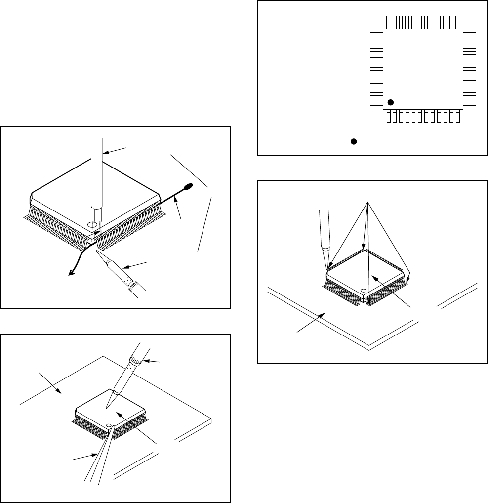
With Iron Wire:
1. Using desoldering braid, remove the solder from
all pins of the flat pack-IC. When you use solder
flux which is applied to all pins of the flat pack-IC,
you can remove it easily. (Fig. S-1-3)
2. Affix the wire to a workbench or solid mounting
point, as shown in Fig. S-1-5.
3. While heating the pins using a fine tip soldering
iron or hot air blower, pull up the wire as the solder
melts so as to lift the IC leads from the CBA
contact pads as shown in Fig. S-1-5.
4. Bottom of the flat pack-IC is fixed with glue to the
CBA; when removing entire flat pack-IC, first apply
soldering iron to center of the flat pack-IC and heat
up. Then remove (glue will be melted). (Fig. S-1-6)
5. Release the flat pack-IC from the CBA using
tweezers. (Fig. S-1-6)
Note: When using a soldering iron, care must be
taken to ensure that the flat pack-IC is not
being held by glue. When the flat pack-IC is
removed from the CBA, handle it gently
because it may be damaged if force is applied.
2. Installation
1. Using desoldering braid, remove the solder from
the foil of each pin of the flat pack-IC on the CBA
so you can install a replacement flat pack-IC more
easily.
2. The “●” mark on the flat pack-IC indicates pin 1.
(See Fig. S-1-7.) Be sure this mark matches the 1
on the PCB when positioning for installation. Then
presolder the four corners of the flat pack-IC. (See
Fig. S-1-8.)
3. Solder all pins of the flat pack-IC. Be sure that
none of the pins have solder bridges.
To Solid
Mounting Point
Soldering Iron
Iron Wire
or
Hot Air Blower
Fig. S-1-5
Fine Tip
Soldering Iron
CBA
Flat Pack-IC
Tweezers
Fig. S-1-6
Example :
Pin 1 of the Flat Pack-IC
is indicated by a " " mark. Fig. S-1-7
Presolder
CBA
Flat Pack-IC
Fig. S-1-8
1-4-4 TVDVDN_SN
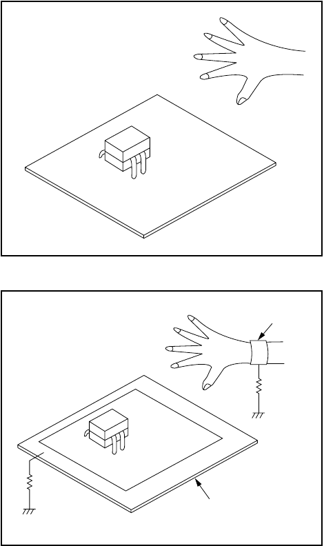
Instructions for Handling Semi-
conductors
Electrostatic breakdown of the semi-conductors may
occur due to a potential difference caused by
electrostatic charge during unpacking or repair work.
1. Ground for Human Body
Be sure to wear a grounding band (1 MΩ) that is
properly grounded to remove any static electricity that
may be charged on the body.
2. Ground for Workbench
Be sure to place a conductive sheet or copper plate
with proper grounding (1 MΩ) on the workbench or
other surface, where the semi-conductors are to be
placed. Because the static electricity charge on
clothing will not escape through the body grounding
band, be careful to avoid contacting semi-conductors
with your clothing.
<Incorrect>
CBA
Grounding Band
Conductive Sheet or
Copper Plate
1MΩ
1MΩ
<Correct>
CBA
1-5-1 T2203PFS
PREPARATION FOR SERVICING
How to Enter the Service Mode
Caution 1:
1. Optical sensors system are used for Tape Start
and End Sensor on this equipment. Read this
page carefully and prepare as described on this
page before starting to service; otherwise, the unit
may operate unexpectedly.
Preparing 1:
1. Cover Q1202 (START SENSOR) and Q1201
(END SENSOR) with Insulation Tape or enter the
service mode to activate Sensor Inhibition
automatically.
Note: Avoid playing, rewinding or fast forwarding the
tape to its beginning or end, because both
Tape End Sensors are not active.
How to Enter the Service Mode
1. Turn power on.
2. Use service remote control unit and press [DISC
MENU] button. (See page 1-7-1.)
3. When entering the service mode, one of the
number (1, 2 or 4) will be displayed at corners of
the screen.
4. During the service mode, electrical adjustment
mode can be selected by remote control key.
(Service remote control unit).
Details are as follows.
Caution 2:
1. The deck mechanism assembly is mounted on the
Main CBA directly, and SW1211 (REC-SAFETY
SW) is mounted on the Main CBA. When deck
mechanism assembly is removed from the Main
CBA due to servicing, this switch can not be
operated automatically.
Preparing 2:
1. To eject the tape, press the [STOP/EJECT] button
on the unit (or Remote Control).
2. When you want to record during the Service
mode, press the [Rec] button while depressing
SW1211 (REC-SAFETY SW) on the Main CBA.
Key Adjustment Mode
PICTURE
Picture adjustment mode: Press the
[PICTURE] button to change from BRT
(Bright), *CNT (Contrast), *COL (Color),
*TNT(Tint), *V-T(V-Tint) and *SHP
(Sharp). Press [CH. o/p] buttons to
display Initial Value.
*Marked items are not necessary to
adjust normally.
0No need to use.
1No need to use.
2H f0 adjustment mode: See adjustment
instructions page 1-7-2.
3No need to use.
4
Auto record mode: Perform recording
(15 Sec.) --> Stop --> Rewind (Zero
return) automatically.
5Head switching position adjustment:
See adjustment instructions page 1-7-6.
6No need to use.
7
Purity check mode: Shows Red, Green,
Blue or White cyclically on the screen
each time the [7] button is pressed.
8H. Position adjustment: See adjustment
instructions page 1-7-5.
9V. Shift/V.Size adjustment: See
adjustment instructions page 1-7-5.
VOL oNo need to use.
VOL p
Cut-off adjustment: See adjustment
instructions page 1-7-3.
White balance adjustment: See
adjustment instructions page 1-7-4.
Key Adjustment Mode
MAIN CBA
Q1201
(END SENSOR)
SW1211
(REC-SAFETY SW)
Q1202
(START SENSOR)
1-6-1 T2202DC
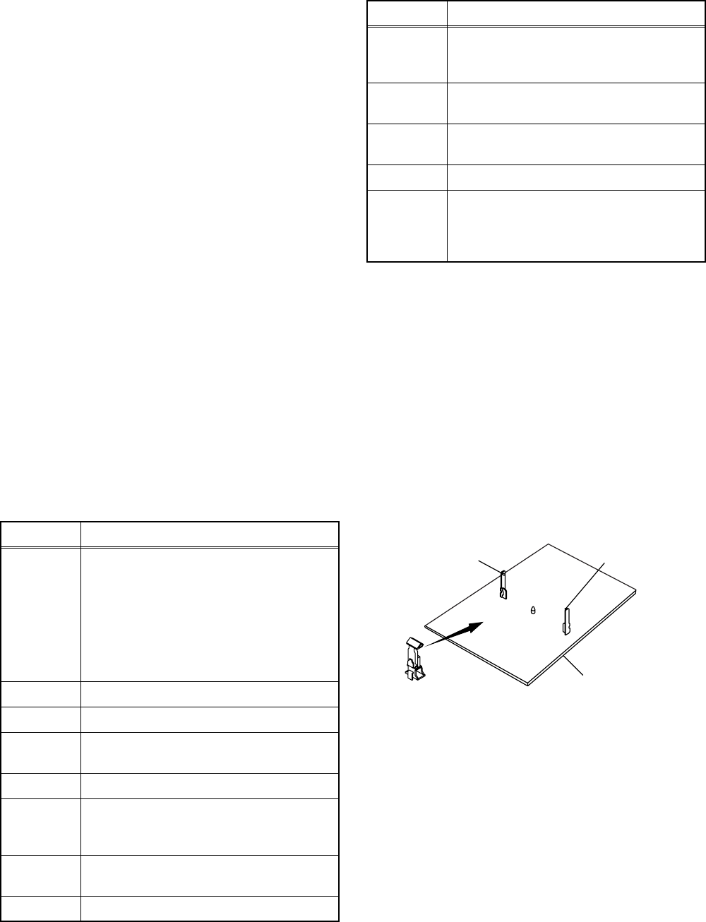
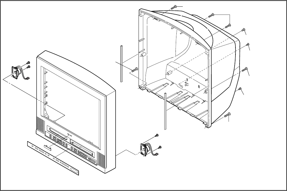
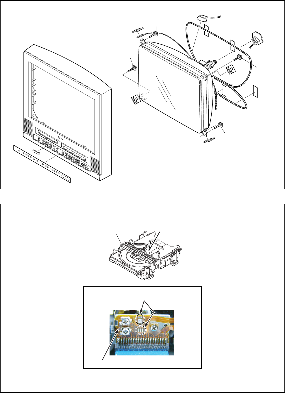
CABINET DISASSEMBLY INSTRUCTIONS
1. Disassembly Flowchart
This flowchart indicates the disassembly steps for the
cabinet parts, and the CBA in order to gain access to
item(s) to be serviced. When reassembling, follow the
steps in reverse order. Bend, route and dress the
cables as they were.
CAUTION!
When removing the CRT, be sure to discharge the
Anode Lead of the CRT with the CRT Ground Wire
before removing the Anode Cap.
2. Disassembly Method
Note:
(1) Order of steps in procedure. When reassembling,
follow the steps in reverse order. These numbers
are also used as the Identification (location) No. of
parts in figures.
(2) Parts to be removed or installed.
(3) Fig. No. showing procedure of part location
(4) Identification of parts to be removed, unhooked,
unlocked, released, unplugged, unclamped, or
desoldered.
P = Spring, L = Locking Tab, S = Screw,
CN = Connector
* = Unhook, Unlock, Release, Unplug, or Desolder
e.g. 2(S-2) = two Screws (S-2),
2(L-2) = two Locking Tabs (L-2)
(5) Refer to the following “Reference Notes in the
Table”.
Step/
Loc.
No.
Part
Removal
Fig.
No.
Remove/*Unhook/
Unlock/Release/
Unplug/Unclamp/
Desolder
Note
[1] Rear
Cabinet D1 6(S-1), (S-2), (S-3A),
(S-3B) ---
[2] Tray
Chassis
Unit
D2
D3
D5
Anode Cap, *CN2501,
CRT CBA, *CN1601,
*CN3802, *CN2571,
*CN3801
1
[3] CRT D3
D5 4(S-4) ---
[4] DVD
Mechanism
D2
D4
D5
4(S-5), *CN201,
*CN301 2, 3
[5] DVD Main
CBA Unit
D2
D4
D5 *CN1, *CN2 ---
[6] Sub CBA D2
D5 5(S-6), *CN1301,
*CN1602, *CL2601 ---
[7] Function
CBA D2
D5 *CN2401 ---
[1] Rear Cabinet
[3] CRT[2] Tray Chassis Unit
[4] DVD
Mechanism
[5] DVD Main
CBA Unit
[6] Sub CBA
[8] Deck Assembly
[9] Main CBA
[7] Function CBA
[8] Deck
Assembly D2
D5
3(S-7), Top Shield,
5(S-8), (S-9), (S-10),
*CL1201, *CL1401,
*CL1402, *CL1403
4
[9] Main CBA D2 5(S-11) ---
↓
(1) ↓
(2) ↓
(3) ↓
(4) ↓
(5)
Step/
Loc.
No.
Part
Removal
Fig.
No.
Remove/*Unhook/
Unlock/Release/
Unplug/Unclamp/
Desolder
Note
1-6-2 T2202DC
Reference Notes in the Table
CAUTION!
When removing the CRT, be sure to discharge the
Anode Lead of the CRT with the CRT Ground Wire
before removing the Anode Cap.
1. CAUTION 1: Discharge the Anode Lead of the
CRT with the CRT Ground Wire before removing
the Anode Cap.
Disconnect the following: Anode Cap, CN2501,
CRT CBA, CN1601, CN3802, CN2571 and
CN3801. Then remove Tray Chassis Unit.
2. CAUTION 2: Electrostatic breakdown of the laser
diode in the optical system block may occur as a
potential difference caused by electrostatic charge
accumulated on cloth, human body etc., during
unpacking or repair work.
To avoid damage of pickup follow next procedures.
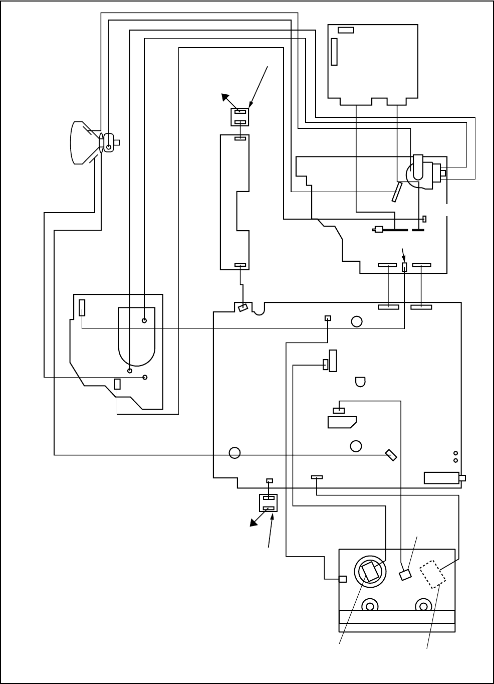
1) Disconnect Connector (CN301) on the DVD
Main CBA Unit.
2) Short the three short lands of FPC cable with
solder before removing the FFC cable (CN201)
from it. If you disconnect the FFC cable
(CN201), the laser diode of pickup will be
destroyed. (Fig. D4)
3) Remove DVD Mechanism.
3. CAUTION 3: When reassembling, confirm the
FFC cable (CN201) is connected completely. Then
remove the solder from the three short lands of
FPC cable. (Fig. D4)
4. Remove three screws (S-7) and remove Top
Shield. Remove screws 5(S-8), (S-9) and (S-10).
Then, desolder connectors (CL1201, CL1401,
CL1402, CL1403) and lift up the Deck Assembly.
[1] Rear Cabinet
(S-1)
(S-1)
(S-1)
(S-1)
(S-3B)
(S-3A)
(S-2)
Fig. D1
(S-1)
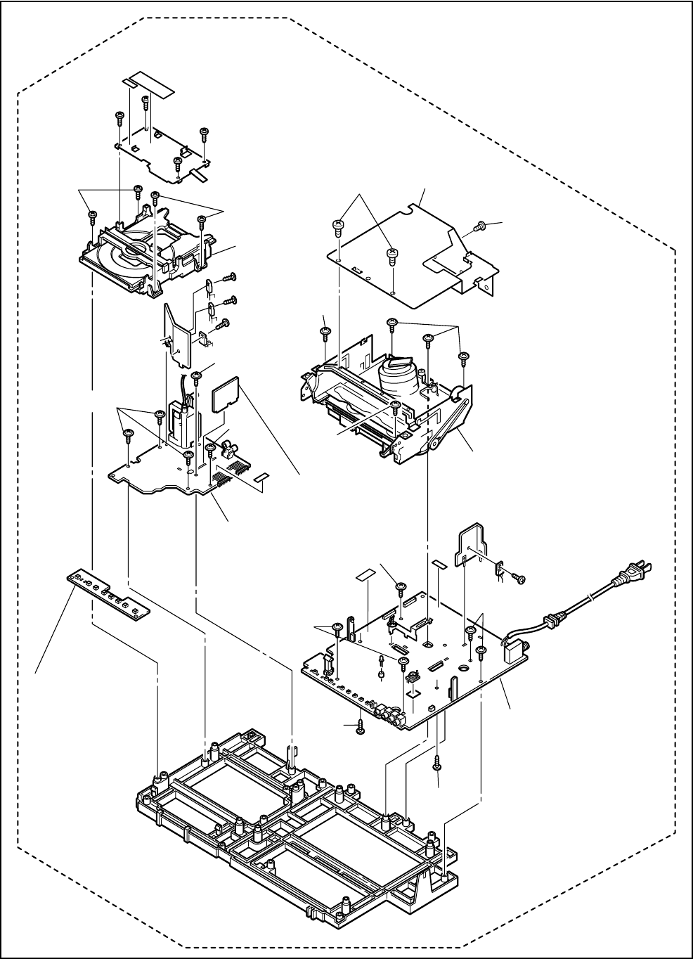
1-6-3 T2202DC
[5] DVD Main
CBA Unit
[4] DVD
Mechanism
[2] Tray Chassis Unit
(S-7)
(S-7)
Top Shield
(S-8)
(S-8)
(S-8)
[8] Deck Assembly
(S-10)
(S-9)
(S-11)
(S-11)
(S-11)
[9] Main CBA
(S-6)
(S-6)
(S-5)
(S-5)
(S-6)
[6] Sub CBA
[7] Function CBA
Fig. D2
1-6-4 T2202DC
[3] CRT
Anode Cap
CRT CBA
(S-4)
(S-4)
(S-4)
(S-4)
Fig. D3
A
DVD Mechanism
Fig. D4
View for A
Short the three short lands by soldering.
(Either of two places.)
FPC Cable
1-6-5 T2202DC
ANODE
CRT
GND
DVD MAIN CBA UNIT
FE HEAD
CYLINDER
ASSEMBLY
ACE HEAD
ASSEMBLY
CAPSTAN
MOTOR
DECK ASSEMBLY
TUNER
MAIN CBA
SUB CBA
CRT CBA
TO SPEAKER
TO SPEAKER
CL2504A
SCREEN
CL2501B
FOCUS
CN1802 CL1201
CN1602CN1301
CN1803
CL1402
CN1601
CL1401
CL1403
CL2501A
CN2571
CN2502
CL2601
CN2503
CN2401
CN2801
CL3801
CN3801
CL3802
CN3802
AC CORD
FUNCTION CBA
JUNCTION-B
CBA
JUNCTION-A CBA
Fig. D5
CN201
CN301
CN2 CN1
CN2A CN1A
CN2501
1-7-1 T2202EA
ELECTRICAL ADJUSTMENT INSTRUCTIONS
General Note: “CBA” is abbreviation for
“Circuit Board Assembly.”
Note: Electrical adjustments are required after
replacing circuit components and certain
mechanical parts. It is important to perform
these adjustments only after all repairs and
replacements have been completed.
Also, do not attempt these adjustments unless
the proper equipment is available.
Test Equipment Required
1. NTSC Pattern Generator (Color Bar W/White
Window, Red Color, Dot Pattern, Gray Scale,
Monoscope, Multi-Burst)
2. AC Milli Voltmeter (RMS)
3. Alignment Tape (FL8A, FL8N), Blank Tape
4. DC Voltmeter
5. Oscilloscope: Dual-trace with 10:1 probe,
V-Range: 0.001~50 V/Div,
F-Range: DC~AC-60 MHz
6. Frequency Counter
7. Plastic Tip Driver
8. Color Analyzer
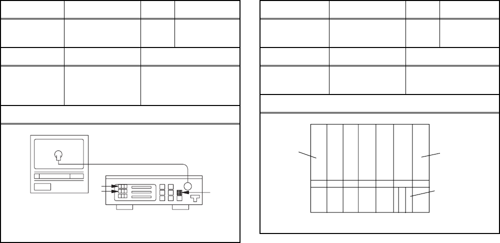
How to make service remote control
unit:
1. Prepare normal remote control unit (Part No.
NE204UD or NE209UD). Remove 4 screws from
the back lid (Fig. 1).
2. Cut off pin 10 of the remote control
microprocessor and short circuit pins 10 and 17 of
the microprocessor with a jumper wire
How to enter the Service mode:
Service mode:
1. Use the service remote control unit.
2. Turn the power on. (Use main power on the TV
unit.)
3. To enter the TV mode, press [CH. o / p] buttons
on the TV unit.
4. Press [DISC MENU] button on the service remote
control unit. Version of micro computer will display
on the CRT. (Ex: BA4-0.16)
X-Ray Protection Test
X-Ray protection test should be done when replacing
any parts of this chassis.
1. Short both ends of R2592 (on Sub CBA).
2. Confirm that the main power turns off.
3. If the main power does not turn off, then replace
the following parts (D2591, Q2591, R2592,
R2593, R2594 and IC1201).
4. Perform steps 1 to 3 again.
1. DC 120V (+B) Adjustment
Purpose: To obtain correct operation.
Symptom of Misadjustment: The picture is dark and
unit does not operate correctly.
Note: TP2501(+B), TP2504(GND) --- Sub CBA,
VR1601 --- Main CBA
1. Connect the unit to AC Power Outlet.
2. Connect DC Volt Meter to TP2501(+B) and
TP2504(GND).
3. Adjust VR1601 so that the voltage of TP2501(+B)
becomes +120±1.0 V DC.
Fig. 1
Screws
Remote control unit (bottom)
Test Point Adj. Point Mode Input
TP2501(+B)
TP2504(GND) VR1601 --- ---
Tape M. EQ. Spec.
--- DC Voltmeter +120±1.0 V DC

1-7-2 T2202EA
2. Setting for CONTRAST, COLOR,
TINT, V-TINT and SHARP Data
Values
General
1. Enter the Service mode. (See page 1-7-1.)
2. Press [PICTURE] button on the service remote
control unit. Display changes “BRT,” “CNT,” “COL,”
“TNT,” “V-T,” and “SHP” cyclically when [PICTURE]
button is pressed.
CONTRAST (CNT)
1. Press [PICTURE] button on the service remote
control unit. Then select “CONTRAST (CNT)”
display.
2. Press [CH. o / p] buttons on the service remote
control unit so that the value of “CONTRAST
(CNT)” becomes 84.
COLOR (COL)
1. Press [PICTURE] button on the service remote
control unit. Then select “COLOR (COL)” display.
2. Press [CH. o / p] buttons on the service remote
control unit so that the value of “COLOR (COL)”
becomes 58.
TINT (TNT)
1. Press [PICTURE] button on the service remote
control unit. Then select “TINT (TNT)” display.
2. Press [CH. o / p] buttons on the service remote
control unit so that the value of “TINT (TNT)”
becomes 45.
V-TINT (V-T)
1. Press [PICTURE] button on the service remote
control unit. Then select “V-TINT (V-T)” display.
2. Press [CH. o / p] buttons on the service remote
control unit so that the value of “V-TINT (V-T)”
becomes 49.
SHARP (SHP)
1. Press [PICTURE] button on the service remote
control unit. Then select “SHARP (SHP)” display.
2. Press [CH. o / p] buttons on the service remote
control unit so that the value of “SHARP (SHP)”
becomes 46.
Note: BRIGHT data value does not need to be
adjusted because this setting is performed in
other setting.
3. H f0 Adjustment
Purpose: To get correct horizontal position and size of
screen image.
Symptom of Misadjustment: Horizontal position and
size of screen image may not be properly displayed.
Note: R2583 --- Sub CBA
1. Connect frequency counter to R2583.
2. Operate the unit for at least 20 minutes.
3. Enter the Service mode. (See page 1-7-1.) Press
[2] button on the remote control unit and select H-
ADJ mode.
4. Press [CH. o / p] buttons on the remote control
unit so that the display will change “0” to “7.”
5. At this moment, choose display “0” to “7” when the
frequency counter display is closest to 15.734 kHz
± 300 Hz.
Test Point Adj. Point Mode Input
R2583 [CH. o / p] buttons Video ---
Tape M. EQ. Spec.
--- Frequency Counter 15.734 kHz±300 Hz
1-7-3 T2202EA
4. Cut-off Adjustment
Purpose: To adjust the beam current of R, G, B, and
screen voltage.
Symptom of Misadjustment: White color may be
reddish, greenish or bluish.
Notes: Screen Control --- FBT (Sub CBA),
FBT = Fly Back Transformer,
Use the Remote Control Unit.
1. Degauss the CRT and allow the unit to operate for
20 minutes before starting the alignment.
2. Input the Black raster signal from RF input.
3. Enter the Service mode. (See page 1-7-1.)
4. Press the [VOL p] button.
(Press [VOL p] button then display will change
“C/D”, “7F” and Initial Setting.)
5. Choose CUT OFF/DRIVE mode then press [1]
button. This adjustment mode is CUT OFF (R).
6. Increase the screen control so that the horizontal
line just appears on the CRT.
7. Press the [CH. o / p] buttons until the horizontal
line becomes white.
8. Choose CUT OFF/DRIVE mode then press [2]
button. This adjustment mode is CUT OFF (G).
Press [CH. o / p] buttons until the horizontal line
becomes white.
9. Choose CUT OFF/DRIVE mode then press [3]
button. This adjustment mode is CUT OFF (B).
Press [CH. o / p] buttons until the horizontal line
becomes white.
5. H. Size Adjustment
Purpose: To obtain correct size of screen image.
Symptom of Misadjustment: Size of screen image
may not be properly displayed.
Note: VR2531 --- Sub CBA
1. Input monoscope pattern.
2. Adjust VR2531 so that the monoscope pattern is
90+1%/-5% of display size and the circle is round.
6. H. Pincushion Adjustment
Purpose: To obtain straight line on the screen.
Symptom of Misadjustment: Straight line image may
not be properly displayed.
Note: VR2530 --- Sub CBA
1. Input crosshatch pattern.
2. Adjust VR2530 so that the lines of the crosshatch
pattern become straight.
Test Point Adj. Point Mode Input
--- Screen-Control
[CH. o / p]
buttons RF Black
Raster
Tape M. EQ. Spec.
--- Pattern
Generator See Reference
Notes below.
Figure
Fig. 2
Pattern Generator
RF Input
Test point Adj. Point Mode Input
--- VR2531 --- Monoscope
Tape M. EQ. Spec.
--- Pattern Generator 90+1%/-5%
Test point Adj. Point Mode Input
--- VR2530 --- Crosshatch
Tape M. EQ. Spec.
--- Pattern Generator See below
1-7-4 T2202EA
7. White Balance Adjustment
Purpose: To mix red, green and blue beams correctly
for pure white.
Symptom of Misadjustment: White becomes bluish
or reddish.
Note: Use service remote control unit
1. Operate the unit more than 20 minutes.
2. Face the unit to the east. Degauss the CRT using
a degaussing coil.
3. Input the White Raster (APL 100%).
4. Set the color analyzer to the CHROMA mode and
after zero point calibration, bring the optical
receptor to the center on the tube surface (CRT).
5. Enter the Service mode. Press [VOL p] button on
the service remote control unit and select “C/D”
mode. (Display changes “C/D”, “7F” and Initial
Setting cyclically when [VOL p] button is pressed.)
6. Press [4] button on the service remote control unit
for Red adjustment. Press [5] button on the service
remote control unit for Blue adjustment.
7. In each color mode, press [CH. o / p] buttons to
adjust the values of color.
8. Adjust Red and Blue color so that the temperature
becomes 9200K (x: 286 / y: 294) ±3%.
9. At this time, re-check that horizontal line is white. If
not, re-adjust Cut-off Adjustment until the
horizontal line becomes pure white.
10. Turn off and on again to return to normal mode.
Receive APL 100% white signal and confirm that
Chroma temperatures become 9200K (x: 286 / y:
294) ±3%.
Note: Confirm that Cut Off Adj. is correct after this
adjustment, and attempt Cut Off Adj. if needed.
8. Sub-Brightness Adjustment
Purpose: To get proper brightness.
Symptom of Misadjustment: If Sub-Brightness is
incorrect, proper brightness cannot be obtained by
adjusting the Brightness Control.
Note: SMPTE Setup level --- 7.5 IRE
1. Enter the Service mode. (See page 1-7-1.)
Then input SMPTE signal from RF input.
2. Press [PICTURE] button. (Press [PICTURE]
button then display will change BRT, CNT, COL,
TNT, V-T, and SHP). Select BRT and press [CH. o
/ p] buttons so that the bar is just visible (See
above figure).
Test Point Adj. Point Mode Input
Screen [CH. o / p]
buttons RF White Raster
(APL 100%)
Tape M. EQ. Spec.
--- Pattern
Generator,
Color analyzer See below
Figure
Fig. 3
Color Analyzer
Test Point Adj. Point Mode Input
--- [CH. o / p]
buttons --- SMPTE
7.5IRE
Tape M. EQ. Spec.
--- Pattern
Generator See below
Figure
Fig. 4
White Black
This bar
just
visible

1-7-5 T2202EA
9. Focus Adjustment
Purpose: Set the optimum Focus.
Symptom of Misadjustment: If Focus Adjustment is
incorrect, blurred images are shown on the display.
Note: Focus VR --- FBT (Sub CBA),
FBT = Fly Back Transformer
1. Operate the unit more than 30 minutes.
2. Face the unit to the East and degauss the CRT
using a degaussing coil.
3. Input the monoscope pattern.
4. Adjust the Focus Control on the FBT to obtain a
clear picture.
10. H. Position Adjustment
Purpose: To obtain correct horizontal position of
screen image.
Symptom of Misadjustment: H. position may not be
properly displayed.
1. Enter the Service mode. (See page 1-7-1.)
Press [8] button on the remote control unit and
select H-P mode.
2. Input monoscope pattern.
3. Press [CH. o / p] buttons on the remote control
unit so that the left and right side of the
monoscope pattern are equal to each other.
11. V. Shift Adjustment
Purpose: To obtain correct vertical position of screen
image.
Symptom of Misadjustment: If V. position is
incorrect, vertical position of image on the screen may
not be properly displayed.
1. Enter the Service mode. (See page 1-7-1.)
Press [9] button on the remote control unit and
select V-P mode. (Press [9] button then display will
change to V-P and V-S).
2. Input monoscope pattern.
3. Press [CH. o / p] buttons on the remote control
unit so that the top and bottom of the monoscope
pattern are equal to each other.
12. V. Size Adjustment
Purpose: To obtain correct vertical height of screen
image.
Symptom of Misadjustment: If V. Size is incorrect,
vertical height of image on the screen may not be
properly displayed.
1. Enter the Service mode. (See page 1-7-1.)
Press [9] button on the remote control unit and
select V-S mode. (Press [9] button then display will
change to V-P and V-S).
2. Input monoscope pattern.
3. Press [CH. o / p] buttons on the remote control
unit so that the monoscope pattern is 90±5% of
display size and the circle is round.
Test Point Adj. Point Mode Input
--- Focus Control --- Monoscope
Tape M. EQ. Spec.
--- Pattern Generator See below
Test Point Adj. Point Mode Input
--- [CH. o / p]
buttons --- Monoscope
Tape M. EQ. Spec.
--- Pattern Generator ---
Test Point Adj. Point Mode Input
--- [CH. o / p]
buttons --- Monoscope
Tape M. EQ. Spec.
--- Pattern Generator ---
Test Point Adj. Point Mode Input
--- [CH. o / p]
buttons --- Monoscope
Tape M. EQ. Spec.
--- Pattern Generator 90±5%
1-7-6 T2202EA
13. Head Switching Position
Adjustment
Purpose: Determine the Head Switching Position
during Playback.
Symptom of Misadjustment: May cause Head
Switching Noise or Vertical Jitter in the picture.
Note: Unit reads Head Switching Position
automatically and displays it on the screen (Upper Left
Corner).
1. Playback test tape (VFMS0001H6).
2. Enter the Service mode. (See page 1-7-1.)
Then press the number [5] button on the remote
control unit.
3. The Head Switching position will display on the
screen; if adjustment is necessary follow step 4.
6.5H(412.7µs) is preferable.
4. Press [CH. o] or [CH. p] button on the remote
control unit if necessary. The value will be
changed in 0.5H steps up or down. Adjustable
range is up to 9.5H. If the value is beyond
adjustable range, the display will change as:
Lower out of range: 0.0H
Upper out of range: -.-H
The following 2 adjustments normally are not
attempted in the field. They should be done only
when replacing the CRT then adjust as a
preparation.
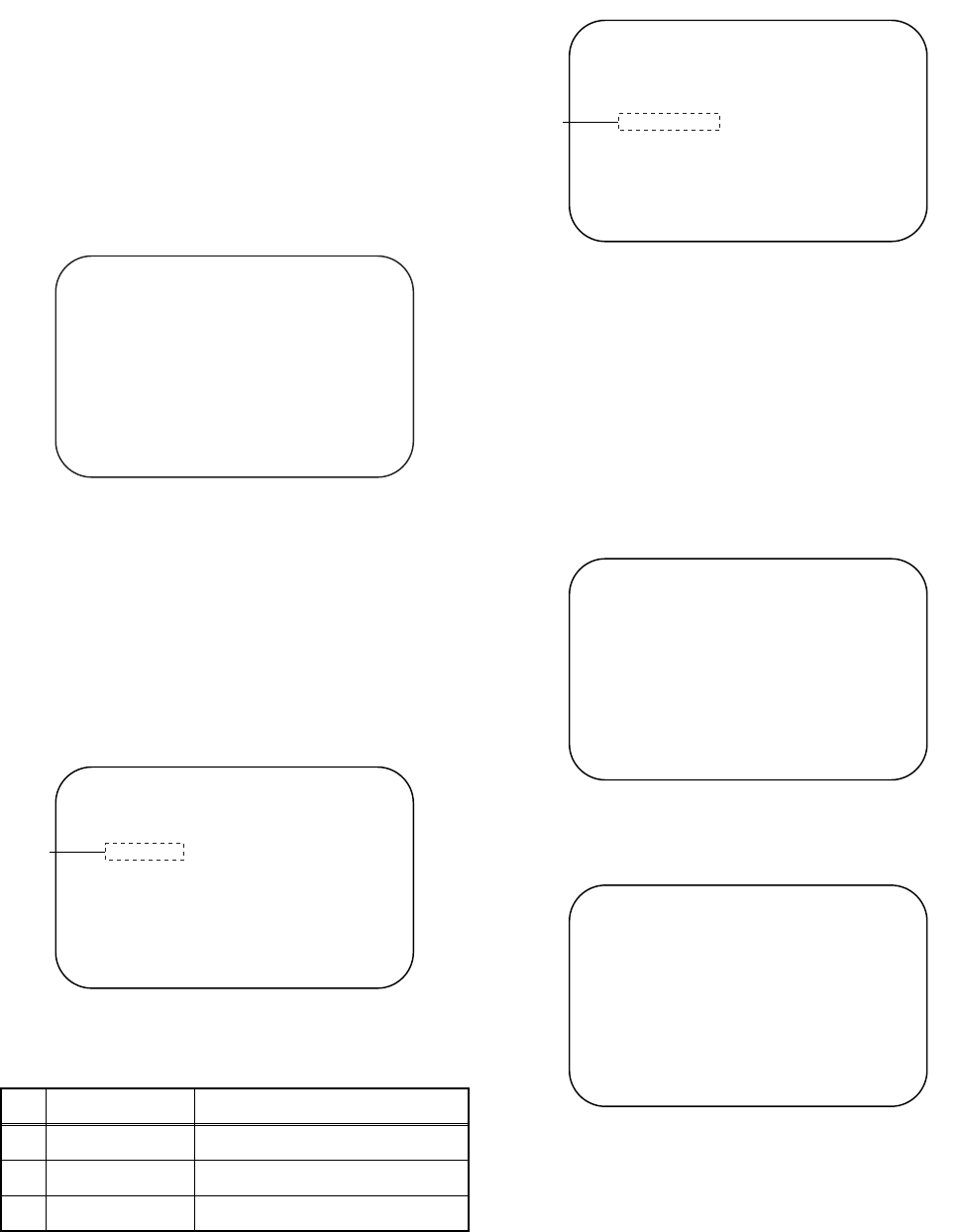
14. Purity Adjustment
Purpose: To obtain pure color.
Symptom of Misadjustment: If Color Purity
Adjustment is incorrect, large areas of color may not
be properly displayed.
* This becomes RED COLOR if the [7] button is
pressed while in service mode.
1. Set the unit facing east.
2. Operate the unit for over 30 minutes before
adjusting.
3. Fully degauss the unit using an external
degaussing coil.
4. Set the unit to the AUX mode which is located
before CH2 then input a red raster from video in.
5. Loosen the screw on the Deflection Yoke Clamper
and pull the Deflection Yoke back away from the
screen. (See Fig. 6.)
6. Loosen the Ring Lock and adjust the Purity
Magnets so that a red field is obtained at the
center of the screen. Tighten Ring Lock. (See Fig.
5, 6.)
7. Slowly push the Deflection Yoke toward the bell of
the CRT and set it where a uniform red field is
obtained.
8. Tighten the clamp screw on the Deflection Yoke.
Test Point Adj. Point Mode Input
--- Deflection Yoke
Purity Magnet --- *Red Color
Tape M. EQ. Spec.
--- Pattern Generator See below
Figure
Fig. 5
GREEN RED BLUE
1-7-7 T2202EA
15. Convergence Adjustment
Purpose: To obtain proper convergence of red, green
and blue beams.
Symptom of Misadjustment: If Convergence
Adjustment is incorrect, the edge of white letters may
have color edges.
1. Set the unit to the AUX mode which is located
before CH2 then input a dot or crosshatch pattern.
2. Loosen the Ring Lock and align red with blue dots
or crosshatch at the center of the screen by
rotating (RB) C.P. Magnets. (See Fig. 7.)
3. Align red / blue with green dots at the center of the
screen by rotating (RB-G) C.P. Magnet.
(See Fig. 8.)
4. Fix the C.P. Magnets by tightening the Ring Lock.
5. Remove the DY Wedges and slightly tilt the
Deflection Yoke horizontally and vertically to
obtain the best overall convergence.
6. Fix the Deflection Yoke by carefully inserting the
DY Wedges between CRT and Deflection Yoke.
Test Point Adj. Point Mode Input
--- C.P. Magnet (RB)
C.P. Magnet (RB-G)
Deflection Yoke --- Dot Pattern
or
Crosshatch
Tape M. EQ. Spec.
--- Pattern Generator See below
Figure
Fig. 6
Fig. 7
Fig. 8
DY WEDGE
DEFLECTION YOKE
C.P. MAGNET
RING LOCK
SCREW
SCREW RB-GRB
PURITY
CRT
COIL
COIL CLAMPER
C.P. MAGNET CLAMPER
B
G
RR
G
B
C.P. MAGNET (RB)
RB
G
RB
G
C.B. MAGNET (RB-G)

1-8-1 T1202NT
HOW TO INITIALIZE THE TV/DVD/VCR
To put the program back at the factory-default, initialize the TV/DVD/VCR as the following procedure.
< DVD Section >
1. Turn the power on and press [SELECT] button on
the remote control unit to put the TV/DVD/VCR
into DVD mode.
2. Press [1], [2], [3], [4], and [DISPLAY] buttons on
the remote control unit in that order.
Fig. a appears on the screen.
3. Press [CLEAR] button on the remote control unit.
Fig. b appears on the screen.
When “OK” appears on the screen, the factory
default will be set.
4. To exit this mode, press [CH. o / p] or [SELECT]
button to go to TV mode, or press [STANDBY-ON]
button to turn the power off.
< TV/VCR Section >
1. Use the service remote control unit.
2. Turn the power on. (Use main power on the TV
unit.)
3. Press [DISC MENU] button on the service remote
control unit to enter the Service mode. (Refer to
“How to enter the Service mode” on page 1-7-1.)
4. Press [VOL p] button on the service remote
control unit twice, and confirm that OSD indication
is “7F = FF.” If needed, set it to become “7F = FF”
by pressing [CH. o / p] buttons on the service
remote control unit.
5. Confirm that OSD indication on the four corners
on TV screen changes from on and off light
indication to red by pressing a [DISPLAY] button.
(It is necessary for one or two seconds.)
6. Turn the power off by pressing main power button
on the TV unit, and unplug the AC cord from the
AC outlet.
MODEL : *******
Version
: *.**
Region
: *
EXIT: SELECTEEPROM CLEAR : CLEAR
Fig. a
"*******" differ depending on the models.
MODEL : *******
Version
: *.**
Region
: *
EEPROM CLEAR : OK
EXIT: SELECTEEPROM CLEAR : CLEAR
"*******" differ depending on the models.
Fig. b
1-9-1 T1202FW
FIRMWARE RENEWAL MODE
1. Turn the power on and press [SELECT] button on
the remote control unit to put the TV/DVD/VCR
into DVD mode. Then remove the disc on the tray.
(It is possible to move to F/W version up mode
only when the TV/DVD/VCR is in DVD mode with
the tray open.)
2. To put the TV/DVD/VCR into F/W version up
mode, press [9], [8], [7], [6], and [MODE] buttons
on the remote control unit in that order.
Fig. a appears on the screen.
The TV/DVD/VCR can also enter the version up
mode with the tray open. In this case, Fig. a will be
shown on the screen while the tray is open.
3. Load the disc for version up.
4. The TV/DVD/VCR enters the F/W version up
mode automatically. Fig. b appears on the screen.
If you enter the F/W for different models, “Disc
Error” will appear on the screen, then the tray will
open automatically.
The appearance shown in (*1) of Fig. b is
described as follows:
5. After programming is finished, the tray opens
automatically. Fig. c appears on the screen and
the checksum will be shown in (*2) of Fig. c.
At this time, no button is available.
6. Remove the disc on the tray.
7. Press [SELECT] button on the remote control unit
to go to TV mode, or press [STANDBY-ON] button
on the unit to turn the power off.
8. Press [SELECT] button on the remote control unit
to put the TV/DVD/VCR into DVD mode again.
9. Press [1], [2], [3], [4], and [DISPLAY] buttons on
the remote control unit in that order.
Fig. d appears on the screen.
10. Press [CLEAR] button on the remote control unit.
Fig. e appears on the screen.
When “OK” appears on the screen, the factory
default will be set. Then the firmware renewal
mode is complete.
11. To exit this mode, press [CH. o / p] or [SELECT]
button to go to TV mode, or press [STANDBY-ON]
button to turn the power off.
No. Appearance State
1 Reading... Sending files into the memory
2 Erasing... Erasing previous version data
3 Programming... Writing new version data
F/W Version Up Mode Model No : *******
VERSION : *.**
Please insert a DISC
for F/W Version Up.
EXIT: SELECT
"*******" differs depending on the models.
Fig. a Version Up Mode Screen
VERSION : ************.ab7
Reading...
F/W Version Up Mode Model No : *******
VERSION : *.**
Fig. b Programming Mode Screen
"*******" differs depending on the models.
(*1)
VERSION : ************.ab7
Completed
SUM : 7ABC
F/W Version Up Mode Model No : *******
VERSION : *.**
"*******" differs depending on the models.
Fig. c Completed Program Mode Screen
(*2)
MODEL : *******
Version
: *.**
Region
: *
EXIT: SELECTEEPROM CLEAR : CLEAR
Fig. d
"*******" differs depending on the models.
MODEL : *******
Version
: *.**
Region
: *
EEPROM CLEAR : OK
EXIT: SELECTEEPROM CLEAR : CLEAR
"*******" differs depending on the models.
Fig. e
1-10-1
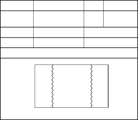
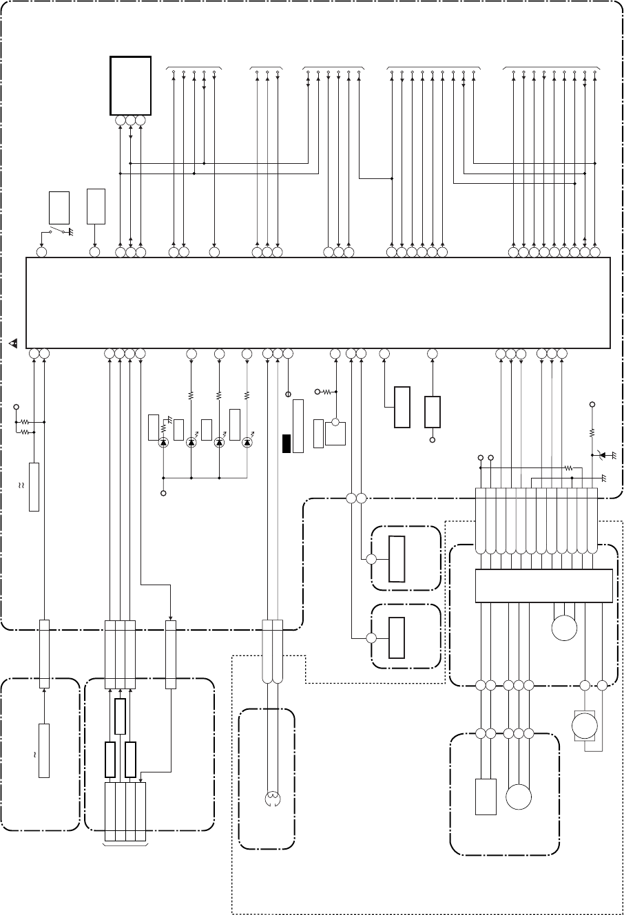
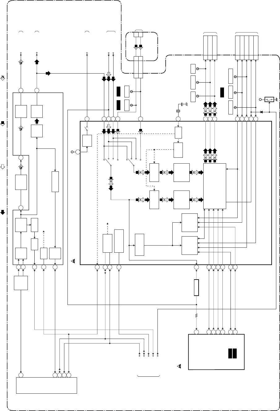
BLOCK DIAGRAMS < TV/VCR Section >
T2202BLS
System Control / Servo Block Diagram
CONTROL
HEAD
CL1402
ACE HEAD ASSEMBLY
MAIN CBA
SUB CBA
RF-SW
T-REEL
DV-SYNC
C-SYNC C-SYNC
V-ENV
CTL(+)
D1224 S-LED
D1204 REC
D1216 DVD
D1217 TV/VCR
REC-LED
KEY0
RS1201
REMOTE
SENSOR
KEY1
DVD-LED
TV/VCR-LED
RESET
ROTA
D-REC-H D-REC-H
REC-SAFETY
AUDIO-MUTE
SCL
REMOTE
SDA
AUDIO-MUTE
CTL(-)
RF-SW
DV-SYNC
V-ENV
ROTA
IC1201(SERVO/SYSTEM CONTROL)
AL+5V
AL+5V
94
95
80
34
18
15
10
13
74
33
8
44
65
72
CTL-AMP-OUT
DVD-REMOTE
97
CTL-AMP-OUT
TP1202
(DECK ASSEMBLY)
T-REEL
Q1206
Q1205
RESET
TIMER+5V
ST/SAP-IN
4NORMAL-H
22
70
YCA-SDA 68
YCA-CS 69
YCA-SCL
YCA-SDA
YCA-CS
SP-MUTE SP-MUTE
12
YCA-SCL
AUDIO-MUTE
DVD-MAIN-POWER
SW1211
REC
SAFETY
TO VIDEO
BLOCK DIAGRAM
TO AUDIO
BLOCK DIAGRAM
TO Hi-Fi AUDIO
BLOCK DIAGRAM
SCL
(MEMORY)
SDA
6
5
P-DOWN 84
P-ON-H P-DOWN
P-ON-H
31
LD-SW1
I
2
C-OPEN 45
71
AL+5V
SW1212
LD-SW
CS
7
TO POWER
SUPPLY BLOCK
DIAGRAM
SDA
SCL TO TV PROCESS
BLOCK DIAGRAM
IC1202
WF3
ENV-DET 17
V-H-SW ENV-DET
V-H-SW
16
SDA
SCL
Hi-Fi-H-SW
ST/SAP-IN
NORMAL-H
DVD-MAIN-POWER
Hi-Fi-H-SW
19
26
2
21
YCA-SDA
YCA-CS
DVD-AUDIO-MUTE
42
5
KEY SWITCH
SW1201 SW1203,
SW1206 SW1210
55KEY1
CN2401
CN2503
CN1803
KEY SWITCH
SW2401 SW2408
14
25
13SDATA
13
18 SDATA
TO DVD SYSTEM
CONTROL/SERVO
BLOCK DIAGRAM
<DVD SECTION>
CN1A
CN1
6
CN1301
14SCLK
15CS
1CM+12V
5
C-CONT
6
FG-GND
7LD-CONT
CAPSTAN MOTOR
P-ON+5V(3)
+26V
M+12V
10M-GND
11D/L+12V
9D-PFG
12VG+15V
END-SENS.
Q1201
SENSOR CBA
(END-SENSOR)
ST-SENS.
Q1202
SENSOR CBA
(ST-SENSOR)
16 SCLK
17 CS
19
DVD-REMOTE
51
52
50
SDATA
SCLK
CS
47
DVD-AUDIO-MUTE
5CTL(+)
6CTL(-)
8D-CONT
4
CM-F/R
3C-FG
2P-ON+5V(3)
66
87
76
82
77
90
C-F/R
C-FG
C-CONT
LD-CONT
D-CONT
D-PFG
CL1201
9
7
ST-SENS.
END-SENS.
14
15
AFT AFT
SPOT-KILL
YCA-SCL
FUNCTION CBA
M
LOADING
MOTOR
CYLINDER ASSEMBLY
DRUM
MOTOR
PG
SENSOR
M
DVD-H DVD-H
48
VOLUME VOLUME
11
Q2203
BUFFER
Q2202
BUFFER
BUFFER
Q2201
19 19
DVD-REMOTE
CN1602
CN2502
MOTOR
DRIVE
CIRCUIT
M
CAPSTAN
MOTOR
41
SPOT-KILL
1-10-2 T2202BLV
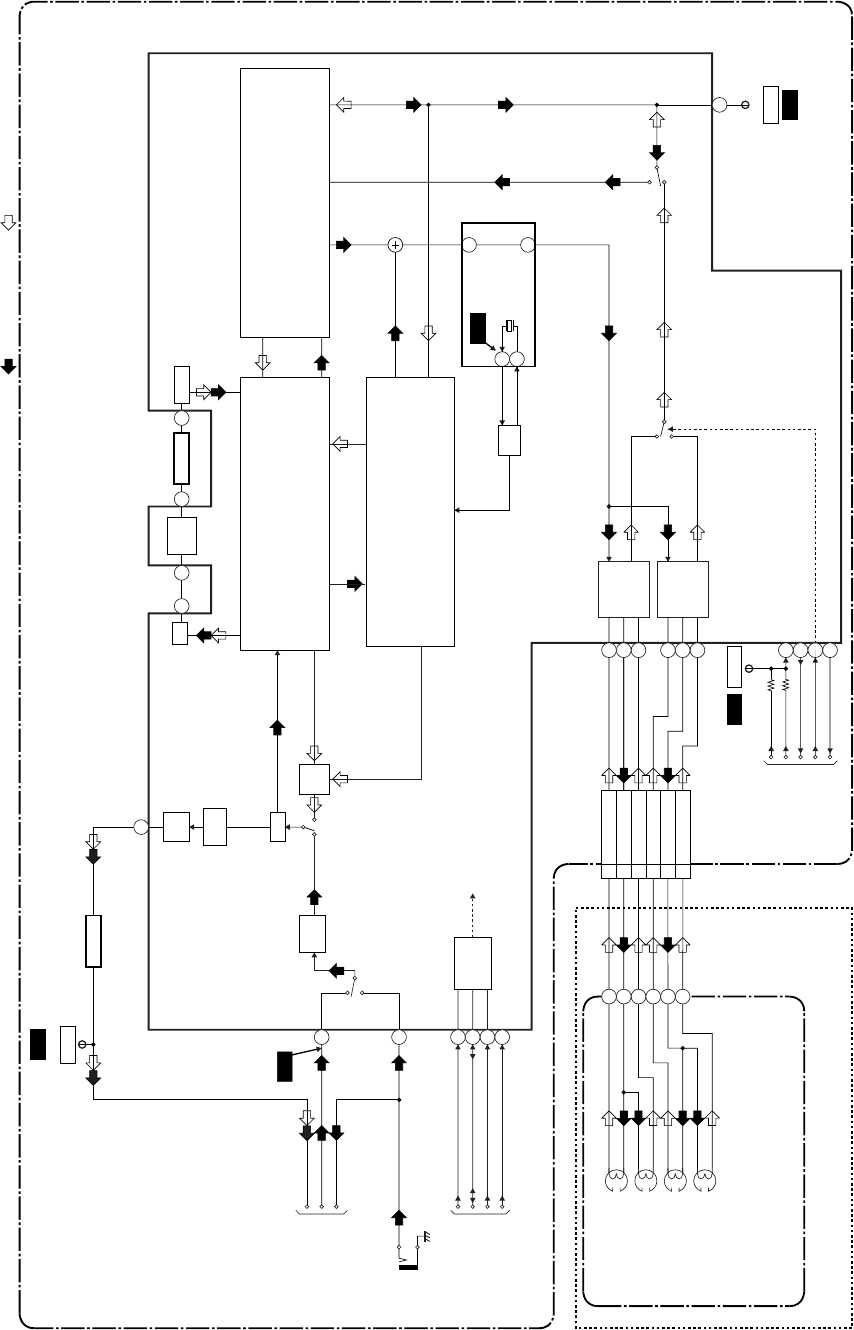
Video Block Diagram
LUMINANCE
SIGNAL PROCESS
MAIN CBA
VIDEO (R)-1 HEAD
VIDEO (L)-1 HEAD
(DECK ASSEMBLY)
VIDEO(R)-1
VIDEO-COM1
VIDEO(L)-1
CL1401
1
2
3
VIDEO(L)-2
VIDEO-COM2
VIDEO(R)-2
4
5
6
Q1401
JK1701
VIDEO-IN
TP1401
V-OUT
VIDEO
AGC
TUNER
LINE
RP
FBC
VXO
Y/C
MIX
CCD 1H
DELAY
R
P
YNR/COMB FILTER
CHROMINANCE
SIGNAL PROCESS
IC1401
(VIDEO SIGNAL PROCESS/ HEAD AMP) 26
REC VIDEO SIGNAL PB VIDEO SIGNAL MODE: SP/REC
57
32
30
QV/QH
6dB
AMP
TO SYSTEM
CONTROL/SERVO
BLOCK DIAGRAM
TO TV PROCESS
BLOCK DIAGRAM
CYLINDER ASSEMBLY
RF-SW
RF-SW
59
V-ENV
V-H-SW
ENV-DET ENV-DET
TP1402
X1401
3.58MHz
VIDEO (L)-2 HEAD
VIDEO (R)-2 HEAD
TP1403
ENV.
BUFFER
DV-SYNC DV-SYNC
53
24
YCA-SCL
VIDEO
TU-VIDEO
EXT-V-IN
14
36 37 39 34
Q1402
BUFFER
58
60
SP
EP
54
YCA-SDA
55
YCA-CS
SERIAL
I/F
VCA CLAMP
69
70
49
50
SP
HEAD
AMP
EP
HEAD
AMP
72
73
74
65
66
67
V-ENV
ROTA
ROTA/RF-SW
WF5
WF4
WF1
WF6
WF2
TO SYSTEM
CONTROL/SERVO
BLOCK DIAGRAM
1-10-3
Audio Block Diagram
T2202BLA
REC
AMP
9
8
AUTO
BIAS
11
P-ON+5V
P-ON+5V
Q1871
BIAS
OSC
Q1872
Q1873
(PB=ON)
Q1874
(PB=ON)
Q1875
SWITCHING
D-REC OFF
6
5
3
EQ
AMP
SP/LP-ON
P
R
ALC
REAR TUNER
FRONT
IC1401
(AUDIO SIGNAL PROCESS) 76
3AUDIO-PB/REC
CL1402
CN1301CN2 CN2503
4 AUDIO-COM
6 AE-H
5 AE-H/FE-H
AUDIO
HEAD
AUDIO
ERASE
HEAD
ACE HEAD ASSEMBLY
FE HEAD
(DECK ASSEMBLY)
1 FE-H
2 FE-H-GND
CL1403
MAIN CBA
SUB CBA
Mode : SP/REC
D-REC-H
TO DVD
AUDIO
BLOCK
DIAGRAM
<DVD
SECTION>
CN2A
FULL
ERASE
HEAD
7880
4
LINE
AMP
LPF MUTE 10
SERIAL
I/F
55 54 53
YCA-CS
YCA-SDA
YCA-SCL
58
AUDIO-MUTE
JK1801
HEADPHONE
JACK
SPEAKER
R-CH
CL3802
CN1803
SP1801
FUNCTION
CBA
SPEAKER
L-CH
CN3801
SP801
SP(R) 1
SP-GND 2
SP(L) 1
SP-GND 2
CL3801
DVD-AUDIO-MUTE
SP-MUTE
19 19
DVD-AUDIO(R)
18
3
418
DVD-AUDIO(L)
TO Hi-Fi AUDIO
BLOCK DIAGRAM
16
9
1
16
DVD-AUDIO-MUTE
AUDIO-OUT(R)
AUDIO-OUT(L)
N-A-IN
N-A-OUT
JK2701
WF19
WF20
WF8
WF7
PB AUDIO SIGNAL
DVD AUDIO SIGNAL
REC AUDIO SIGNAL
DIGITAL
AUDIO-OUT
(COXIAL)
TO SYSTEM
CONTROL/SERVO
BLOCK DIAGRAM
TO SYSTEM
CONTROL/SERVO
BLOCK DIAGRAM
2
11
IC1803 (AUDIO AMP)
7
VOLUME
14
1
AMP
AMP
MUTE
/STANDBY
CONTROL
3
6
8
DVD
DVD
VCR
VCR
(L-CH)
(R-CH)
212
DVD-H
VOLUME
Q2701
BUFFER
Q2619
1,2 1,2
SP(R)
CN1802
JUNCTION-A CBA
CN3802
1,3 1,3
SP(L)
CN2401
1,2 1,2
SP(L)
CN2801
JUNCTION-B CBA
1-10-4
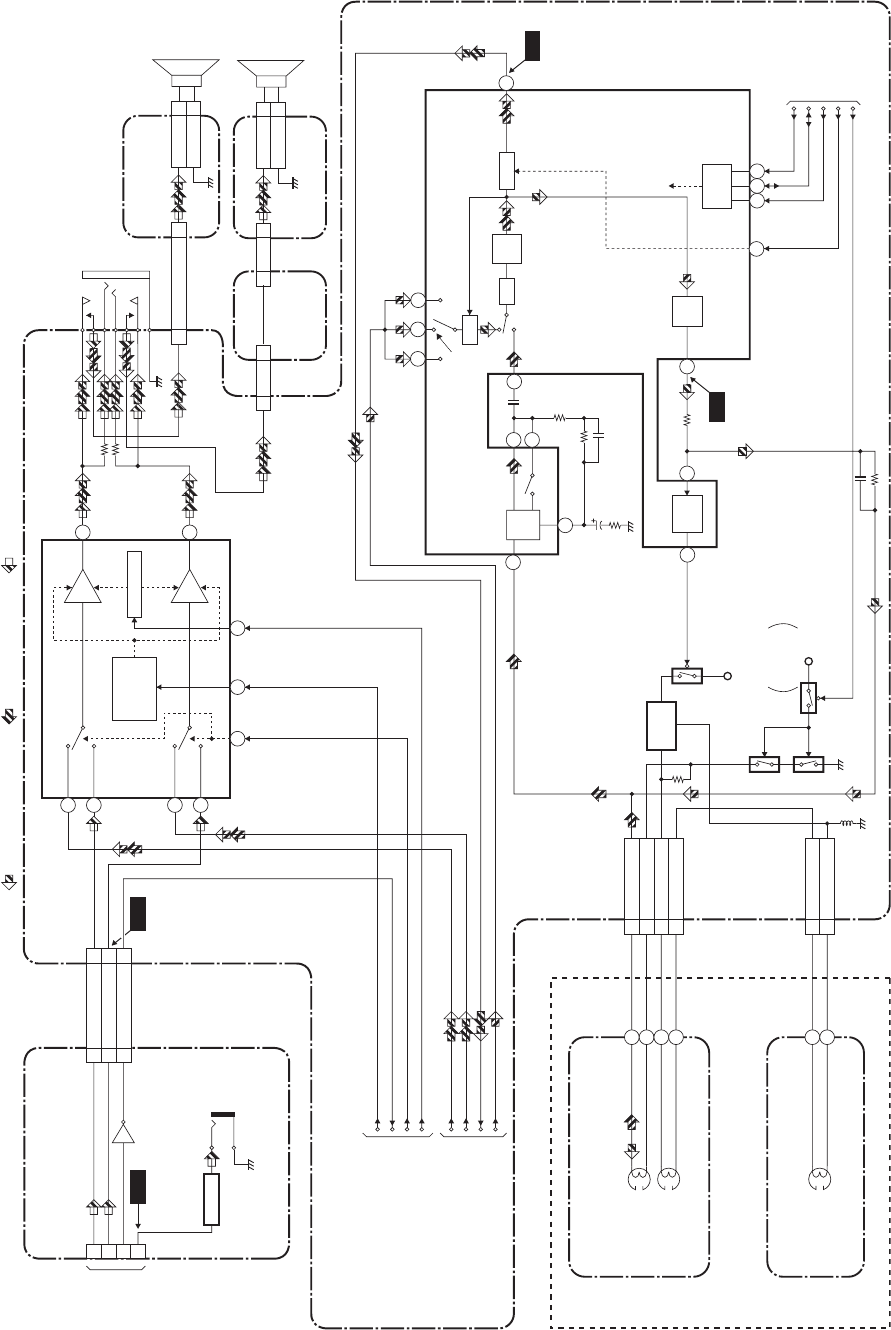
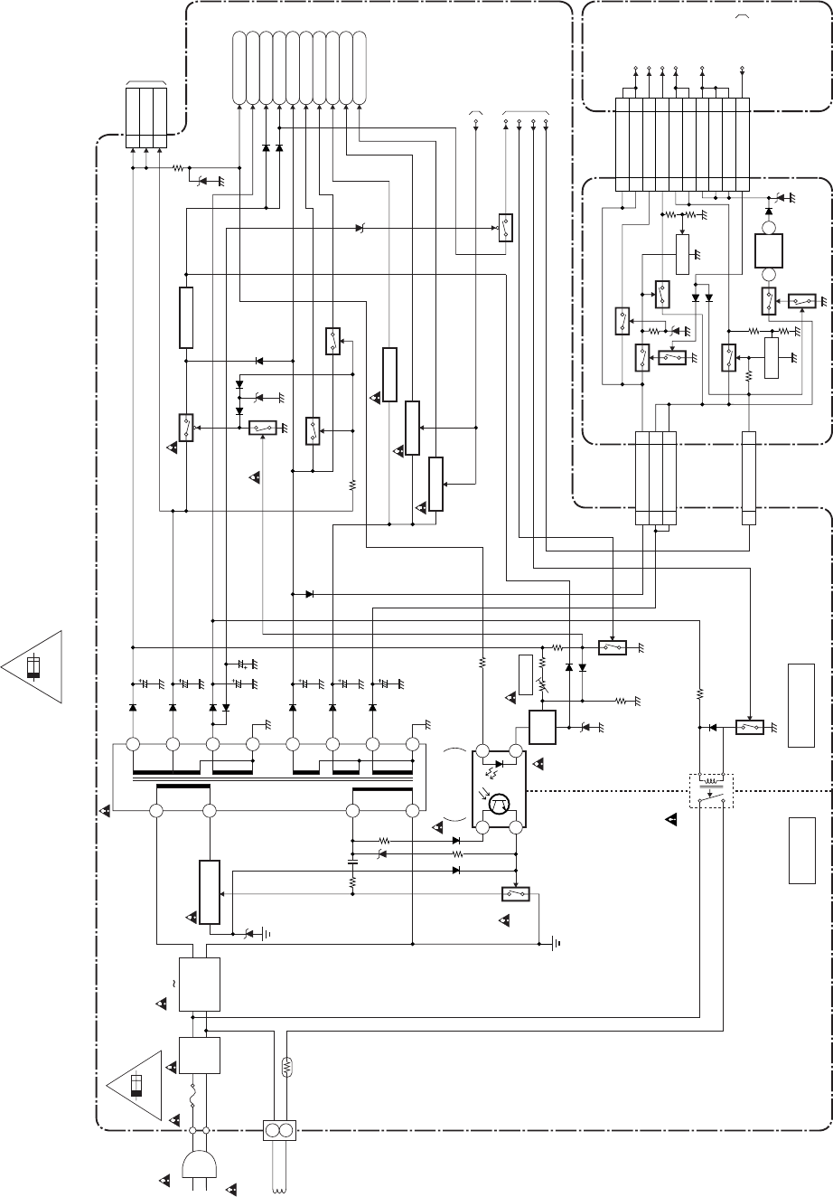
Hi-Fi Audio Block Diagram
T2202BLH
57
48 47
13 14
69
6
7
R-CH
INSEL
L-CH
INSEL
NOR
SW
SERIAL
DATA
DECODER
OUTPUT
SELECT
VCO LPF
L-CH BPF
R-CH
PNR
PILOT
DET
CONT
STEREO
PLL
STEREO
FILTER
SAP
FILTER
SAP
DET
SIF
DEMOD
SAP
DEMOD L-R
DEMOD
ST/SAP
SW MATRIX
L-CH
PNR
LIM DEV
COMP
SW
NOISE
VCO LPF
LIM DEV
COMP
COMP
D.C
NOISE
SW
dBX
DEC
ENV
DET
MODE
OUT
RIPPLE
FILTER
DO
DET
MATRIX
R-CH BPF
P
R
R
L
P
R
HOLD
PULSE
NOISE
DET
34 33
23
4
80
78
37
38
54
77
1
39
26
24
27
N-A-OUT
LIM
49
AUDIO-OUT(L)
AUDIO-OUT(R)
N-A-IN
Hi-Fi-H-SW
AUDIO-MUTE
NORMAL-H
40
ST/SAP-IN
TO AUDIO
BLOCK DIAGRAM
SCL
P-ON+9V
Hi-Fi
AUDIO
(R) HEAD
Hi-Fi
AUDIO
(L) HEAD
CYLINDER
ASSEMBLY
MAIN CBA
CL1401
IC1701 (MTS/ SAP/ Hi-Fi AUDIO PROCESS/ Hi-Fi HEAD AMP)
PILOT
CANCEL
TO AUDIO
BLOCK DIAGRAM
62 63
JK1702
AUDIO(L)-IN
JK1703
AUDIO(R)-IN
SIF
TO TV PROCESS
BLOCK DIAGRAM
Q1701
TP1702 TP1701
SDA
Hi-Fi-L Hi-Fi-R
PB AUDIO SIGNALREC AUDIO SIGNAL Mode : SP/REC
TO SYSTEM
CONTROL/SERVO
BLOCK DIAGRAM
TO SYSTEM
CONTROL/SERVO
BLOCK DIAGRAM
TO SYSTEM
CONTROL/SERVO
BLOCK DIAGRAM
Hi-Fi-
AUDIO(R) 7
Hi-Fi
-COM 8
Hi-Fi-
AUDIO(L) 9
1-10-5
TV Process Block Diagram
T2202BLT
X1301
3.58MHz
CN1301
SAW
FILTER
SF1001
IC1301(CHROMA/DEFLECTION SIGNAL PROCESS)
TU1001
IF
AGC
SDA
SCL
FSC
1
7
3
2
5
IC1201
(SYSTEM CONTROL/OSD)
V-SYNC
H-SYNC
OSD-R
OSD-G
OSD-B
59
58
60
62
63
64
OSD-BLK
SIF TO Hi-Fi AUDIO
BLOCK DIAGRAM
EXT-V-IN
TO VIDEO
BLOCK DIAGRAM
TO DIGITAL
SIGNAL PROCESS
BLOCK DIAGRAM
<DVD SECTION>
CN2A
VIDEO
TO CRT/H.V. BLOCK
DIAGRAM CN2503
TO CRT/H.V. BLOCK
DIAGRAM CN2503
3
GREEN4
BLUE
SDA
AFT
SCL
Mode : SP/REC
WF16
WF15
WF17 WF18
56
CV-IN
5
MAIN CBA
SUB CBA
18
34
35
8
9
31
13
10
11
12
15
14
4
5
3
2
40
41
16
6
20
25
23
29
CHROMA
TRAP
SERIAL
I/F
INTELLIGENT
MONITORING
CHROMA
BPF
SYNC
SEPARATION
LUMA
SIGNAL
PROCESS
CIRCUIT
CHROMA
SIGNAL
PROCESS
CIRCUIT
H-SYNC
PROCESS
CIRCUIT
V-SYNC
PROCESS
CIRCUIT
OSD MIX/RBG MATRIX/
BLIGHT/DRIVE AMP/
HV BLANKING
TUNER
TUNER
FILTER
TUNING VXCO
CF1032
IC1001(IF SIGNAL PROCESS)
VIF
AMP
VIDEO
DET
VCO
4.5MHz
FILTER
IF AGC DET
SIF
AMP
RF
AGC
AMP
AFT EQ
AMP
16
11
13
17 478
14
C-SYNC
SPOT-KILL
LINE
DVD
VCR
VCR
LINE
DVD
RED
CN1301
7
H-DRIVE1
V-DRIVE
8
AFC
2
V-RAMP-NF9
ACL
CN1301 CN2503
10
DVD-C11
10
11
CN2
8
6
DVD-Y
28
Q1403
BUFFER
TP1301
BLUE GREEN RED
TP1302 TP1303
REC VIDEO SIGNAL PB VIDEO SIGNAL DVD VIDEO SIGNAL
REC AUDIO SIGNAL
TO SYSTEM
CONTROL/SERVO
BLOCK DIAGRAM
TU-VIDEO TO VIDEO
BLOCK DIAGRAM
1
SIF
AMP
+5.7V
REG. 27
30
+8V
+5V-CTRL
TO POWER
SUPPLY BLOCK
DIAGRAM
Q1350
P-ON+8V
DVD-Y
TP2513
DVD-C
TP2512
TP1306
V-RAMP
TP1304
V-DRIVE
TP1305
H-OUT
WF9
1-10-6
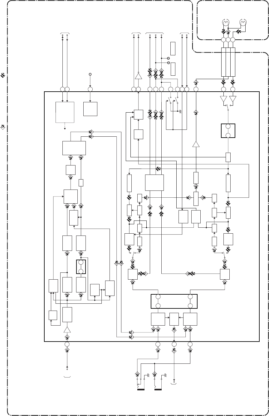
CRT/H.V. Block Diagram
T2202BLCRT
PULSE
UP
AMP
THERMAL
PROTECTION
3
6
7
1
5
8
10
7
9
6
GREEN AMP
BLUE AMP
Q2503 Q2502
Q2501
H.DRIVE
Q2591
Q2571 T2572A
V-
DRIVE
H-
DRIVE
D.Y.
L551
IC2551 (V-DEFLECTION CONTROL)
T2571 F.B.T.
ANODE
FOCUS
SCREEN
CN2503
SUB CBA
CRT CBA
CL2504A
R
G
B
HEATER
ANODE
GND
V501
CRT
GND
FOCUS
SCREEN
JK2501
HEATER 11
CN2501
CL2501BCL2501A
CN2571
+180V 33
11
S
F
HV
FOCUS VR
SCREEN VR
CN2502
4
3
2RED
GREEN
BLUE
H.OUTPUT
1
3
5
4
5
4
3
1
WF13WF12
WF14
WF10
WF11
RED AMP
TP2501
+B
TP2504
GND
TP2506
AFC
TO POWER
SUPPLY
BLOCK
DIAGRAM
CN1602
CN2503 CL2601
2
3
4
RED
5
GREEN
4
BLUE
3
TO TV PROCESS
BLOCK DIAGRAM
CN1301
TO TV
PROCESS
BLOCK
DIAGRAM
CN1301
REC VIDEO SIGNAL PB VIDEO SIGNAL DVD VIDEO SIGNAL
Mode : SP/REC
+B
1
+B
2
+26V
6
V-DRIVE
8
H-DRIVE
1
AFC
7
ACL
2
V-RAMP-NF
9
H.
CONTROL
Q2530,
Q2531
VR2531VR2530
PINC. H SIZE
Q2532
Q2533
1-10-7
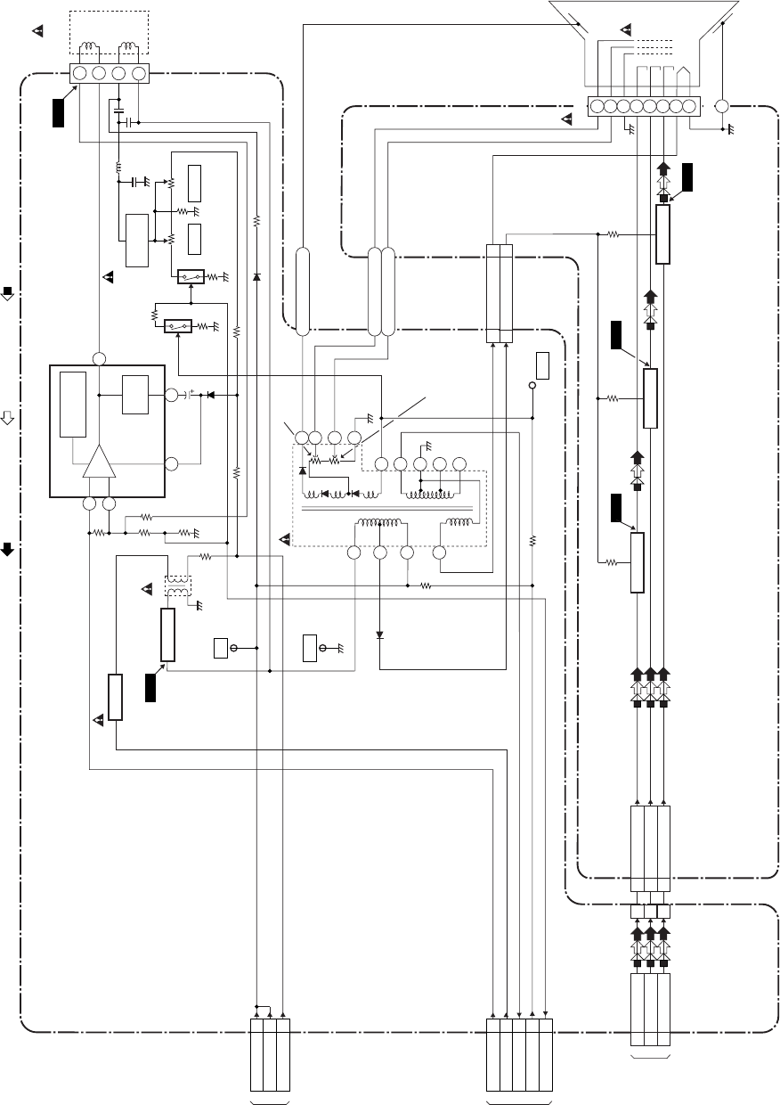
Power Supply Block Diagram
T2202BLP
LINE
FILTER
BRIDGE
RECTIFIER
T1601
IC1601
ERROR
VOLTAGE DET
W1601 F1601
4A/125V
L1601 D1603 D1606
DEGAUSSING
COIL
CN1601
DG601
COLD
SUB CBA
MAIN CBA
SWITCHING
Q1601
Q1604
Q1605
Q1606 Q1609
Q1607
Q1613
Q1614
Q1688
Q1681
Q1221
Q1602 VR1601
+B ADJ
CN1301
CN1602 CN2502
CN2503
P-DOWN
DVD-MAIN-POWER
P-ON-H
TO CRT/H.V.
BLOCK DIAGRAM
CN2502
CN1602
+33V
1
23
4
10
11
17
12
15
16
14
13
9
8
6
3
FEED
BACK
1+B
2+B
8 +26V
M+12V
TIMER+5V
AL+5V
P-ON+12V
P-ON+8V
P-ON+9V
P-ON+5V(2)
P-ON+5V(3)
+5.7V REG.
SW +5V
SW +5V
TO SYSTEM
CONTROL/SERVO
BLOCK DIAGRAM
4A 125V
P-ON+5V(4)
IC1682
+5V REG.
+5.7V-CTRL TO TV PROCESS
BLOCK DIAGRAM
Q2610
Q2612
Q2617
IC2602
IC3603
IC3604
+1.2V
REG.
3 2
Q2615
Q2618
Q2616
Q2611
SW CTL
SW CTL
17 17
DVD-MAIN-POWER
10 10EV+4V
11 11EV+4V
14 14DVD+9V
11 11
DVD-ON+3.3V
10 10EV+3.3V
14 14EV+9V
13 13
EV+9V
12 12
DVD-ON+5V
99EV+3.3V
33EV+1.2V
22EV+1.2V
11EV+1.2V
15 15
PWRCON
DVD MAIN
CBA UNIT
EV+9V
DVD-ON+5V
DVD-ON+3.3V
EV+3.3V
EV+1.2V
PWRCON
CN1A
TO DVD SYSTEM
CONTROL / SERVO
BLOCK DIAGRAM
<DVD SECTION>
HOT
CN1
PS1601
RL1601
Q1603
DG-ON-H
CAUTION !
Fixed voltage (or Auto voltage selectable) power supply circuit is used in this unit.
If Main Fuse (F1601) is blown , check to see that all components in the power supply
circuit are not defective before you connect the AC plug to the AC power supply.
Otherwise it may cause some components in the power supply circuit to fail.
For continued protection against risk of fire,
replace only with same type 4 A, 125V fuse.
CAUTION ! :
ATTENTION : Utiliser un fusible de rechange de même type de 4A, 125V.
4A 125V
NOTE:
The voltage for parts in hot circuit is measured using
hot GND as a common terminal.
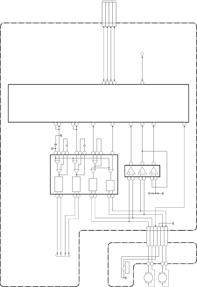
1-10-8
BLOCK DIAGRAMS < DVD Section >
DVD System Control / Servo Block Diagram
T2202BLSD
18
17
16
DVD-REMOTE
19
CN1A
S D ATA
CS
54
53
49
DVD-REMOTE
FP-CLK
FP-DIN
FP-DOUT
55
DVD MAIN CBA UNITDRIVE CBA
IC301 (SERVO DRIVE)
CN301
M
SLED
MOTOR
M
SPINDLE
MOTOR
IC101 (MICRO CONTROLLER)
+
-+
-
+
-
+
-
+
-
+
-
+
-
SLED
MOTOR
DRIVE
FOCUS
ACTUATOR
DRIVE
SPINDLE
MOTOR
DRIVE
TRACKING
ACTUATOR
DRIVE
126
TRAY-IN
SLD
67
SPDL
66
TRACKING
DRIVE
127
FOCUS DRIVE
65
TO DIGITAL SIGNAL
PROCESS BLOCK
DIAGRAM
FS(+)
FS(-)
TS(+)
TS(-)
TRAY-IN
6SP(+)
5SP(-)
1TRAY-IN
4GND
3SL(-)
2SL(+)
VREF
TO SYSTEM CONTROL
/SERVO BLOCK
DIAGRAM
<TV/VCR SECTION>
CN1
15
16
14
13
12
11
17
18 23
6
4
5
3
1
2
25
24
27
26
63
SL-AMP
121
SP-ROT
+3.3V
124
FD-OFST
123
TD-OFST
SCLK
PWRCON PWRCON
46
TO POWER SUPPLY
BLOCK DIAGARAM
<TV/VCR SECTION>
IC202
(OP AMP)
1
2
67
5
3
98
10
SL-ADS
122
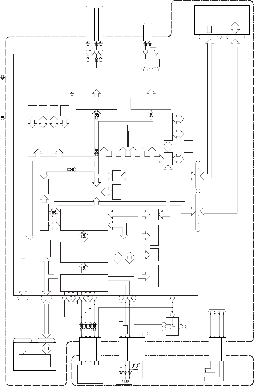
1-10-9
Digital Signal Process Block Diagram
T2202BLD
C16
D18
A17
B15
DVD-LD 8
CD-LD 10
PD-MONI 7
FS(+) 2
FS(-) 3
TS(+) 1
TS(-) 4
CN201
CN201
CN201
IC201
(SW)
IC101 (MICRO CONTROLLER)
FS
FS(+)
CD/DVD
FS(-)
TS(+)
TS(-)
TS
DETECTOR
CD/DVD 19
Q251,Q252
CD DVD
AMP
Q253,Q254
AMP
4
1 3
6
GND(DVD-PD)
6
GND(CD-PD)
5
GND(LD)
9
RF
SIGNAL
PROCESS
CIRCUIT
DVD/CD
FORMATTER
AUDIO
I/F
VIDEO
I/F
NTSC/PAL
ENCODER
DMA
BCU
INST.
ROM 32BIT
CPU
DATA
RAM
INTERRUPT
CONTROLLER
WATCH DOG
TIMER
CPU
I/F
TIMER
DECODER
I/F
CPU
I/F
READ
MEMORY
DATA
RAM
DSP
DECODER
I/O
PROCESSOR
INST.
ROM
DATA
RAM
INST.
ROM
SERIAL
GENERAL
I/O
INTERRUPT
CONTROLLER
TIMER
WATCH DOG
TIMER
REMOTE
CONTROL
32BIT CPU
STREAM
I/F
EXTERNAL
MEMORY
I/F
SDRAM
ECC
UMAC
100
115
116
113
114
106
104
105
103
62
DEBUG
BCU
INST
CACHE
DATA
CACHE
152
151
146
144
SDRAM ADDRESS(0-10)
IC103 (FLASH ROM)
FLASH
ROM
29
36
38
45
~
~
DVD VIDEO SIGNAL
FDQ (0-15)
~
1
9
16
25
48
~
FADR (0-19)
SDRAM DATA(0-15)
PICK-UP
UNIT
TO SYSTEM
CONTROL/SERVO
BLOCK DIAGRAM
DVD MAIN CBA UNIT
IC503 (SDRAM)
SDRAM DATA(0-15)
SDRAM ADDRESS(0-10)
194
209
~
2
13
42
53
~
~
22
26
29
34
~~
159
178
~
99
98
97
21~30 34~42 212
1~4 7~14 17~18 215~216
AUDIO D/A
CONVERTER
131
D/A
D/A
139
Y
C
TO
TV PROCESS
BLOCK
DIAGRAM
<TV/VCR
SECTION>
CN2
CN2A
8 DVD-Y
6 DVD-C
CN2A
TO AUDIO
BLOCK DIAGRAM
<TV/VCR SECTION>
CN2
1 SPDIF
4 DVD-AUDIO(L)
3 DVD-AUDIO(R)
9
DVD-AUDIO-MUTE
DVD AUDIO SIGNAL
1-11-1 X7TN_SC
SCHEMATIC DIAGRAMS / CBA’S AND TEST POINTS
Standard Notes
WARNING
Many electrical and mechanical parts in this chassis
have special characteristics. These characteristics
often pass unnoticed and the protection afforded by
them cannot necessarily be obtained by using
replacement components rated for higher voltage,
wattage, etc. Replacement parts that have these
special safety characteristics are identified in this
manual and its supplements; electrical components
having such features are identified by the mark “#” in
the schematic diagram and the parts list. Before
replacing any of these components, read the parts list
in this manual carefully. The use of substitute
replacement parts that do not have the same safety
characteristics as specified in the parts list may create
shock, fire, or other hazards.
Notes:
1. Do not use the part number shown on these
drawings for ordering. The correct part number is
shown in the parts list, and may be slightly
different or amended since these drawings were
prepared.
2. All resistance values are indicated in ohms
(K = 103, M = 106).
3. Resistor wattages are 1/4W or 1/6W unless
otherwise specified.
4. All capacitance values are indicated in µF
(P = 10-6 µF).
5. All voltages are DC voltages unless otherwise
specified.
1-11-2 X7TN_SC
LIST OF CAUTION, NOTES, AND SYMBOLS USED IN THE SCHEMATIC DIAGRAMS ON
THE FOLLOWING PAGES:
1. CAUTION: FOR CONTINUED PROTECTION AGAINST RISK OF FIRE, REPLACE ONLY
WITH SAME TYPE_A,_V FUSE.
ATTENTION: UTILISER UN FUSIBLE DE RECHANGE DE MÊME TYPE DE_A,_V.
2. CAUTION:
Fixed Voltage (or Auto voltage selectable) power supply circuit is used in this unit.
If Main Fuse (F1601) is blown, first check to see that all components in the power supply circuit are not defec-
tive before you connect the AC plug to the AC power supply. Otherwise it may cause some components in the
power supply circuit to fail.
3. Note:
1. Do not use the part number shown on the drawings for ordering. The correct part number is shown in the
parts list, and may be slightly different or amended since the drawings were prepared.
2. To maintain original function and reliability of repaired units, use only original replacement parts which are
listed with their part numbers in the parts list section of the service manual.
4. Mode: SP/REC
5. Voltage indications for PLAY and REC modes on the schematics are as shown below:
6. How to read converged lines
7. Test Point Information
231 5.0
(2.5)
PLAY mode
STOP mode
5.0
The same voltage for
both PLAY & STOP modes Indicates that the voltage
is not consistent here.
< DVD Section >
231 5.0
(2.5)
< 0 >
PLAY mode
REC mode
DVD mode
5.0
The same voltage for
PLAY, REC & DVD
modes Indicates that the voltage
is not consistent here.
< TV/VCR Section > Unit: Volts
3
2
1
ABCD
1-B1
1-D3
AREA D3
AREA B1
1-D3
Distinction Area
Line Number
(1 to 3 digits)
Examples:
1. "1-D3" means that line number "1" goes to the line number
"1" of the area "D3".
2. "1-B1" means that line number "1" goes to the line number
"1" of the area "B1".
: Indicates a test point with a jumper wire across a hole in the PCB.
: Used to indicate a test point with a component lead on foil side.
: Used to indicate a test point with no test pin.
: Used to indicate a test point with a test pin.
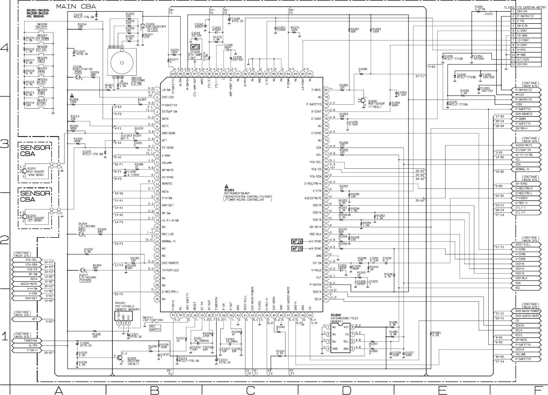
1-11-3
Main 1/6 & Sensor Schematic Diagram < TV/VCR Section >
T2202SCM1
1-11-4 T2202SCM2
Main 2/6 Schematic Diagram < TV/VCR Section >
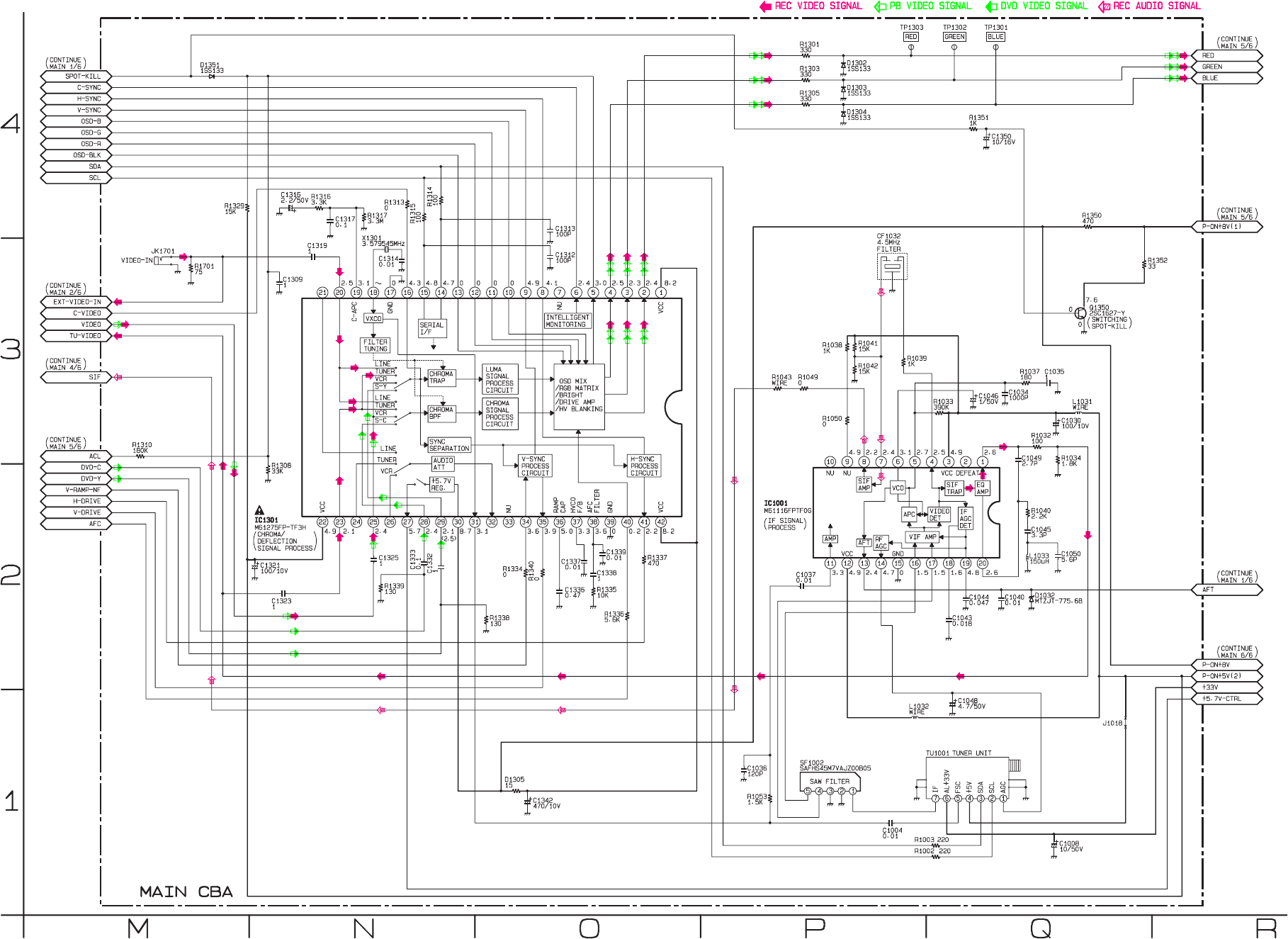
1-11-5 T2202SCM3
Main 3/6 Schematic Diagram < TV/VCR Section >
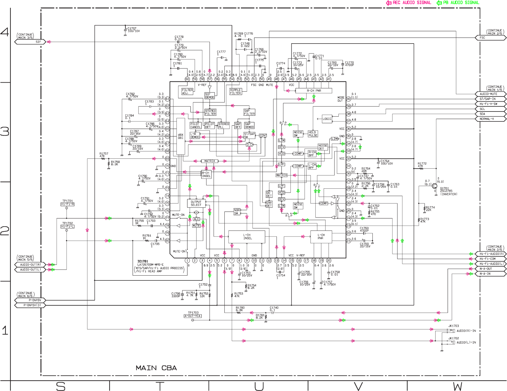
1-11-6
Main 4/6 Schematic Diagram < TV/VCR Section >
T2202SCM4
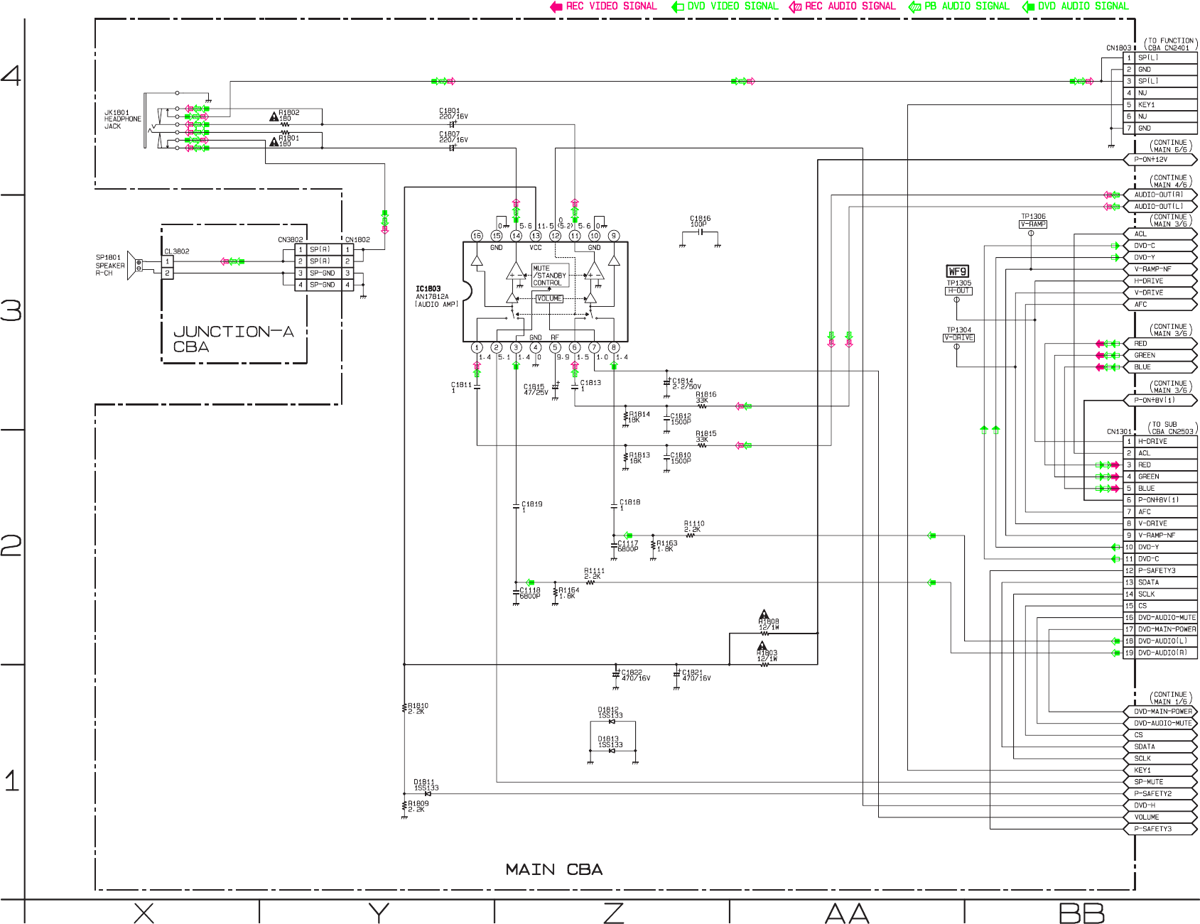
1-11-7 T2202SCM5
Main 5/6 & Junction-A Schematic Diagram < TV/VCR Section >
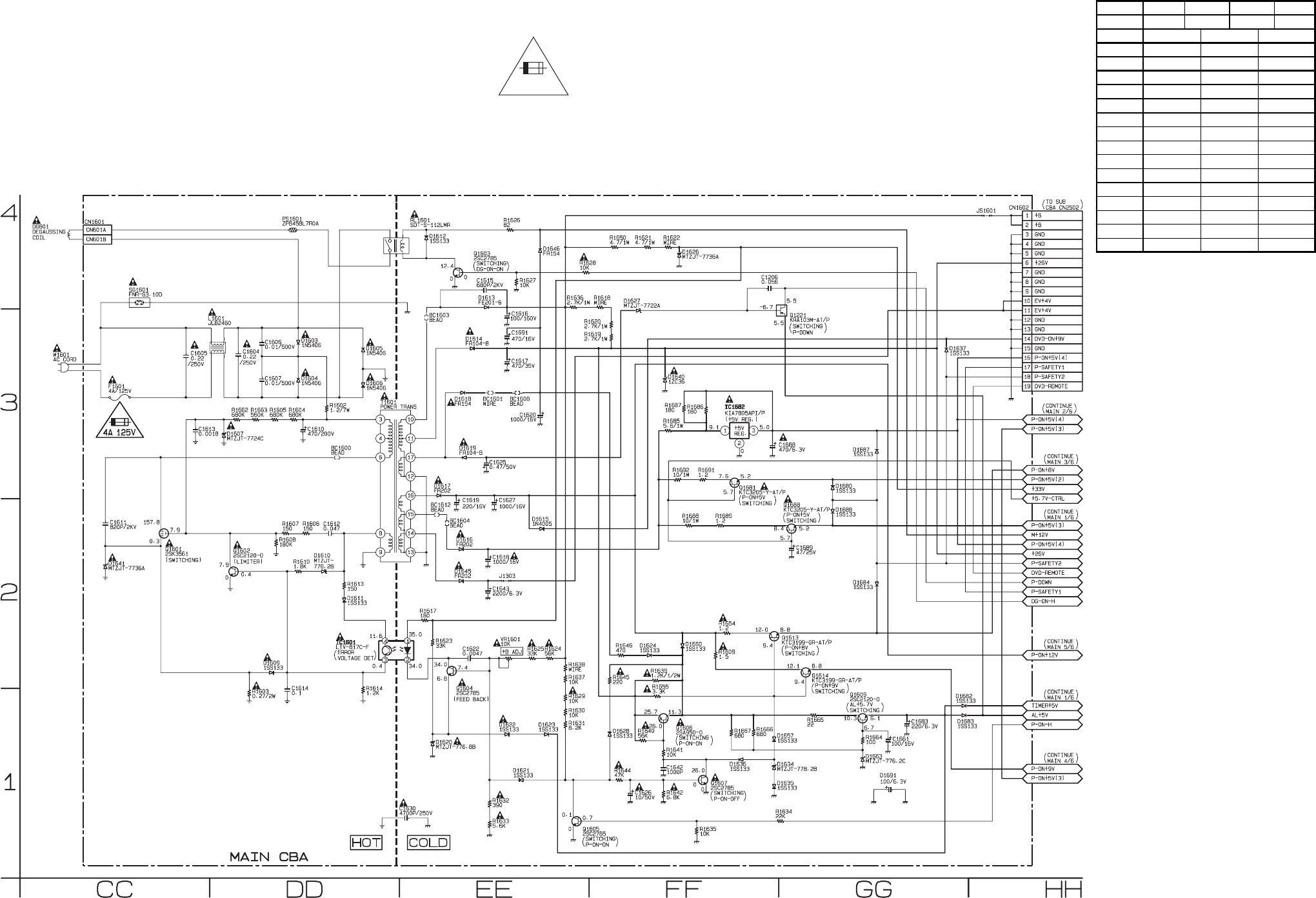
1-11-8 T2202SCM6
Main 6/6 Schematic Diagram < TV/VCR Section >
NOTE:
The voltage for parts in hot circuit is measured using
hot GND as a common terminal.
For continued protection against risk of fire,
replace only with same type 4 A, 125V fuse.
CAUTION ! :
ATTENTION : Utiliser un fusible de rechange de même type de 4A, 125V.
4A 125V
CAUTION !
Fixed voltage (or Auto voltage selectable) power supply circuit is used in this unit.
If Main Fuse (F1601) is blown , check to see that all components in the power supply
circuit are not defective before you connect the AC plug to the AC power supply.
Otherwise it may cause some components in the power supply circuit to fail.
VOLTAGE CHART (Power off mode)
Ref. No. 1 4
IC1601 25.7 1.2
Ref. No.
IC1682
Ref. No.
Q1601
Ref. No.
Q1221
Q1602
Q1604
Q1605
Q1606
Q1607
Q1609
Q1613
Q1614
Q1681
Q1688
23
24.7 0.3
123
3.2 0 1.7
SDG
0 162.8 1.9
ECB
5.2 5.1 4.6
01.90.3
6.7 24.7 7.3
07.90
8.5 8.5 7.8
07.76.6
5.9 8.2 6.5
0.8 4.2 1.4
0.9 4.2 1.4
03.30
03.30
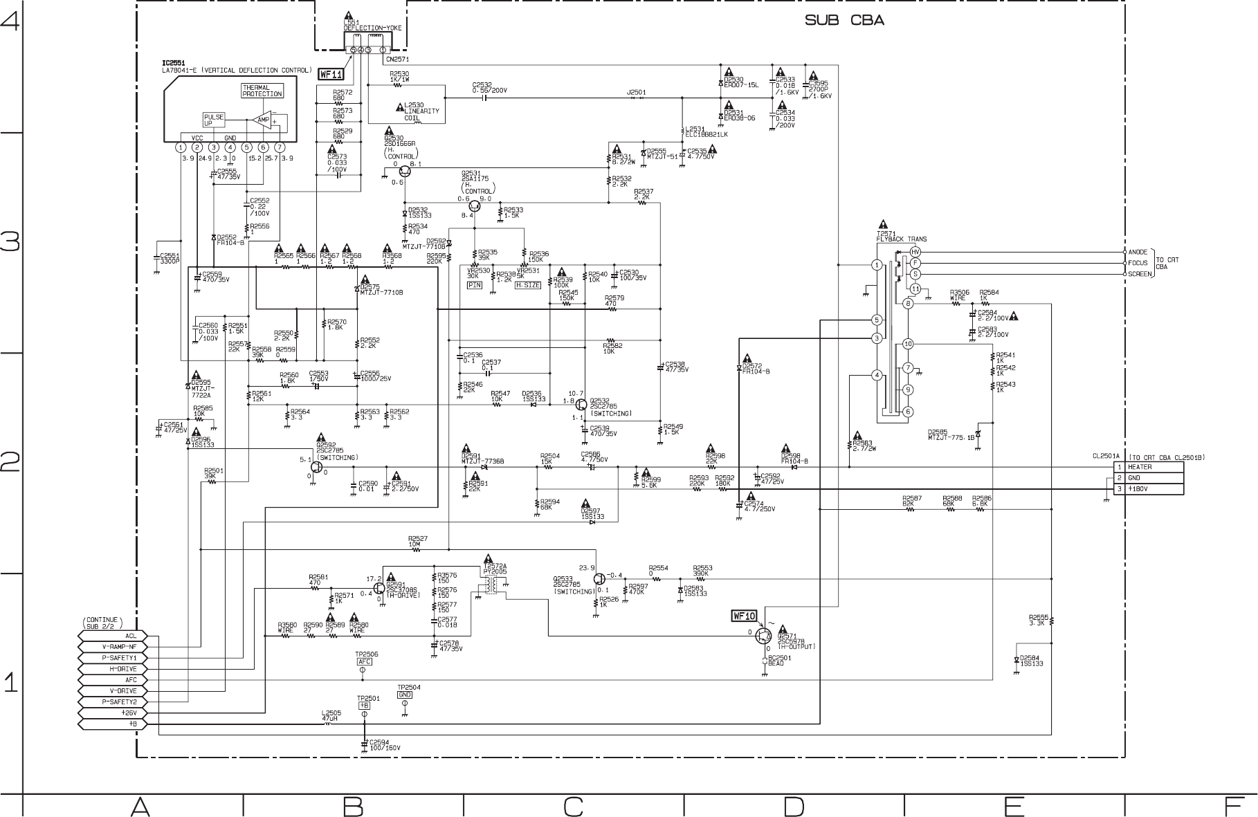
1-11-9 T2202SCSUB1
Sub 1/2 Schematic Diagram < TV/VCR Section >
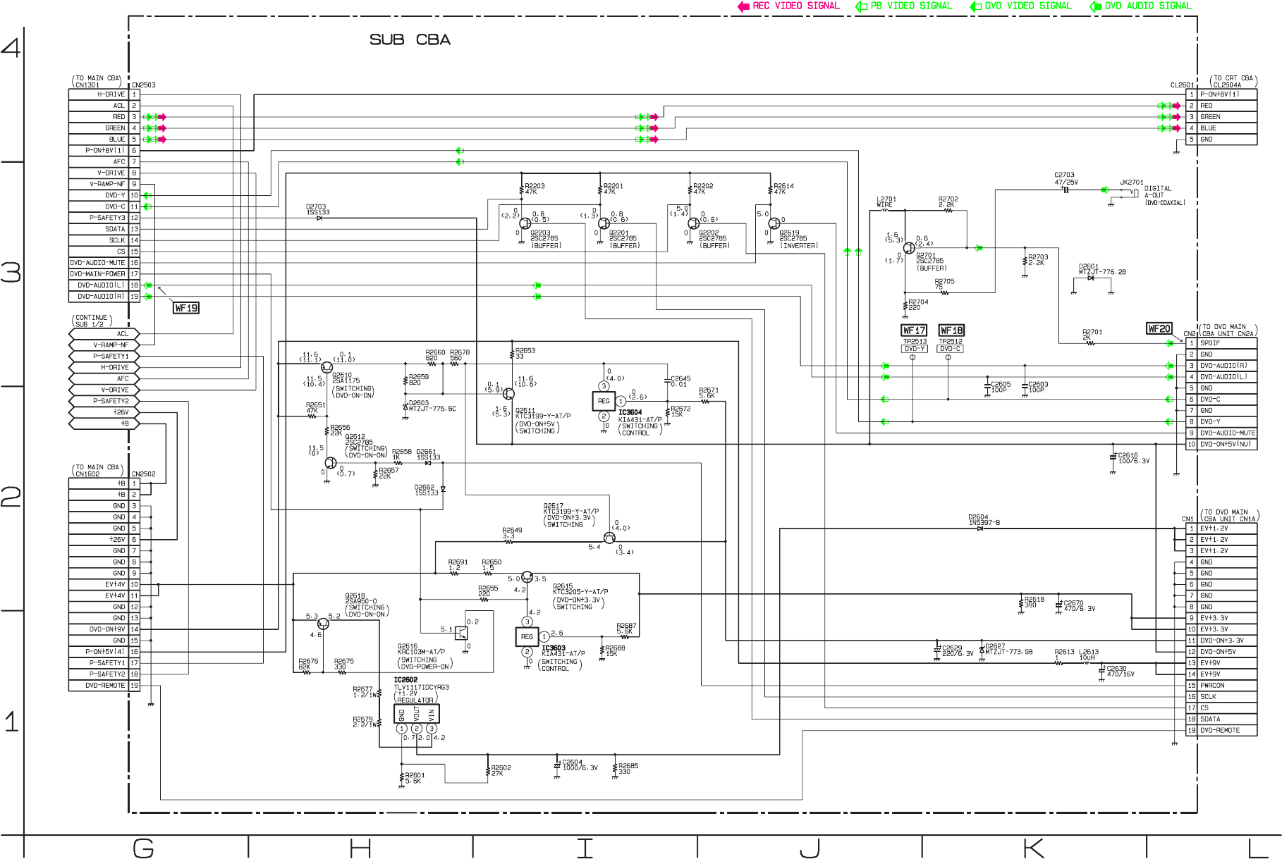
1-11-10
Sub 2/2 Schematic Diagram < TV/VCR Section >
T2202SCSUB2
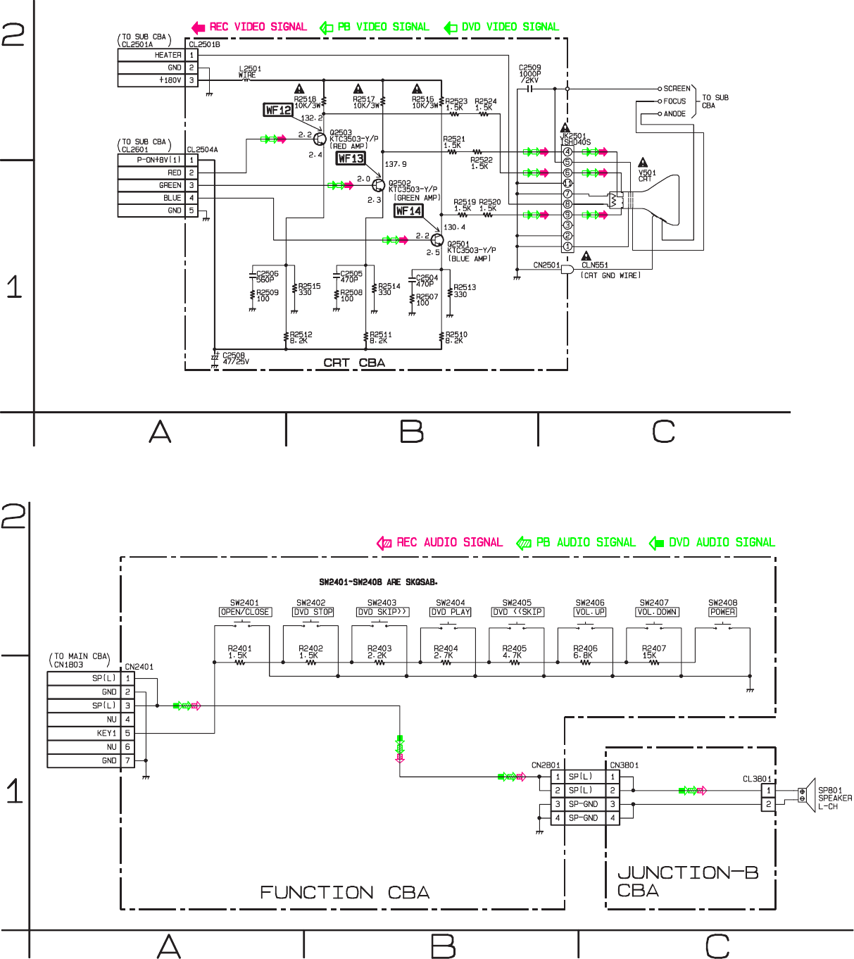
1-11-11
T2202SCCRT
T2202SCF
Function & Junction-B Schematic Diagram < TV/VCR Section >
CRT Schematic Diagram < TV/VCR Section >
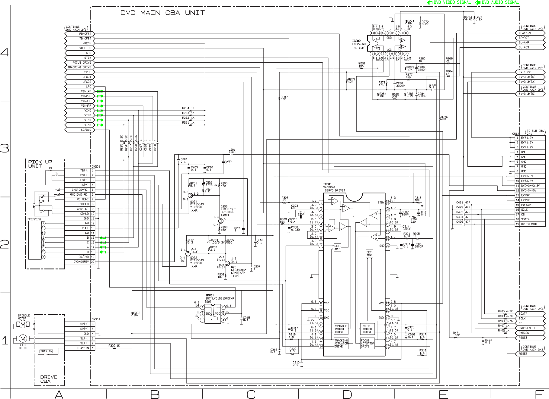
1-11-12 T2202SCD1
DVD Main 1/3 Schematic Diagram < DVD Section >
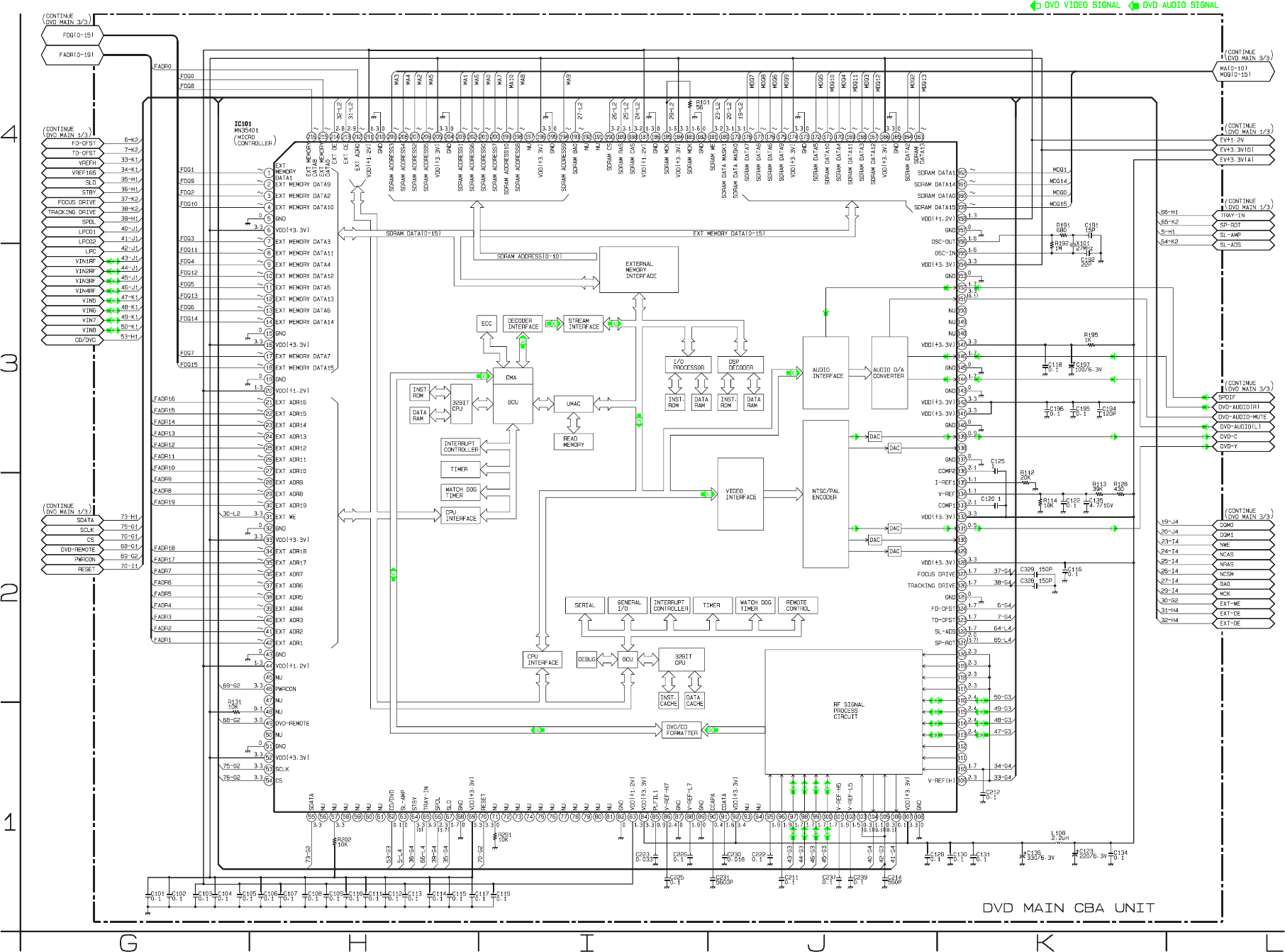
1-11-13 T2202SCD2
DVD Main 2/3 Schematic Diagram < DVD Section >
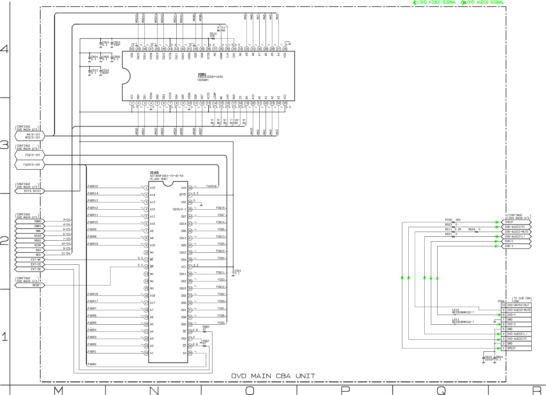
1-11-14 T2202SCD3
DVD Main 3/3 Schematic Diagram < DVD Section >
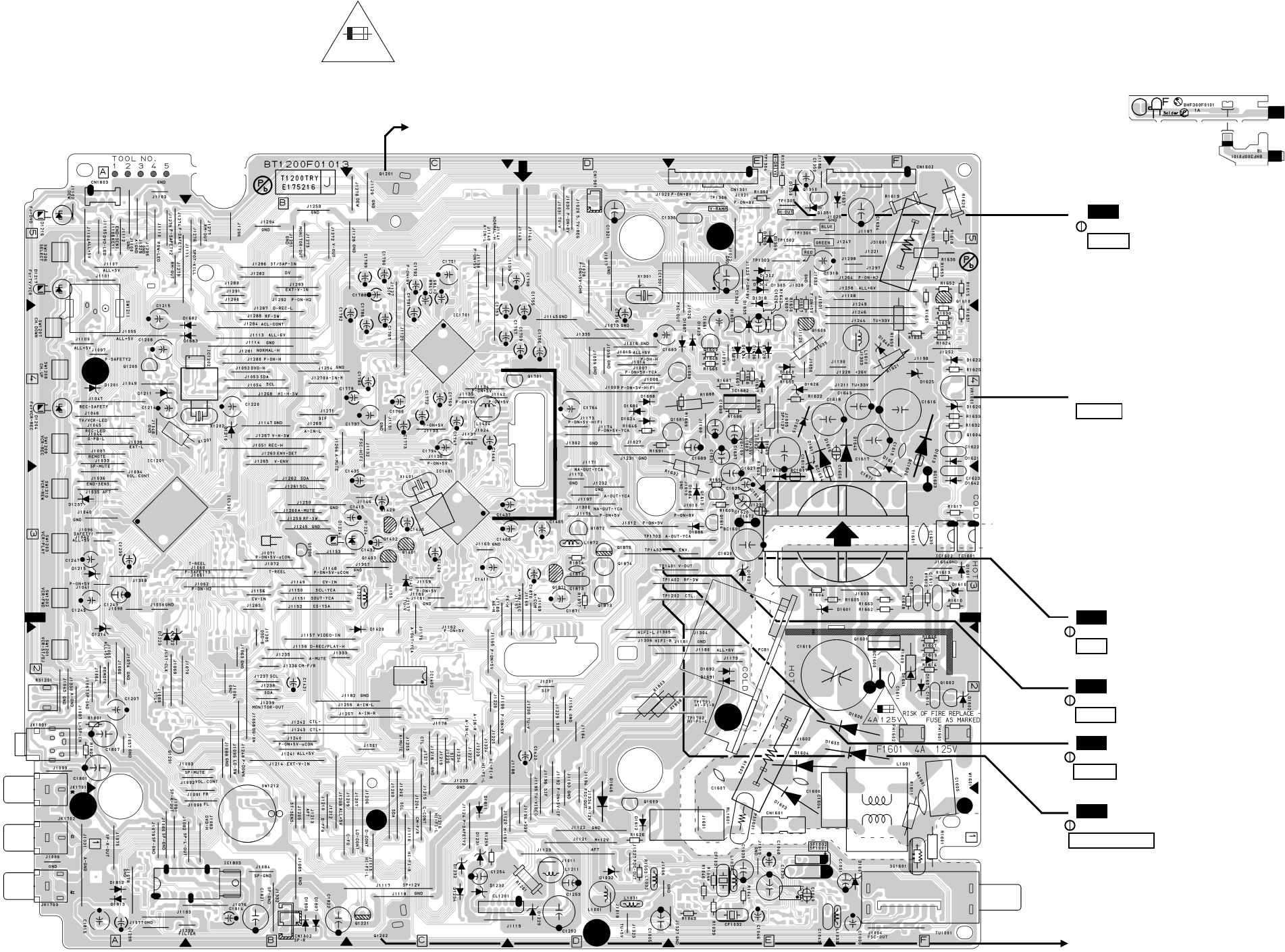
1-11-15
V-OUT
TP1401
WF5
TO SENSOR CBA
(START-SENSOR)
RF-SW
TP1402
WF1
CTL-AMP-OUT
TP1202
WF3
ENV.
TP1403
WF6
+B ADJ
VR1601
H-OUT
TP1305
WF9
TO SENSOR CBA
(END-SENSOR)
Main CBA Top View < TV/VCR Section >
BT1200F01013
Because a hot chassis ground is present in the power
supply circuit, an isolation transformer must be used.
Also, in order to have the ability to increase the input
slowly,when troubleshooting this type power supply
circuit, a variable isolation transformer is required.
NOTE:
The voltage for parts in hot circuit is measured using
hot GND as a common terminal.
For continued protection against risk of fire,
replace only with same type 4 A, 125V fuse.
CAUTION ! :
ATTENTION : Utiliser un fusible de rechange de même type de 4A, 125V.
4A 125V
CAUTION !
Fixed voltage (or Auto voltage selectable) power supply circuit is used in this unit.
If Main Fuse (F1601) is blown , check to see that all components in the power supply
circuit are not defective before you connect the AC plug to the AC power supply.
Otherwise it may cause some components in the power supply circuit to fail.
BHF300F01011A
BHF300F01011B
Sensor CBA Top View
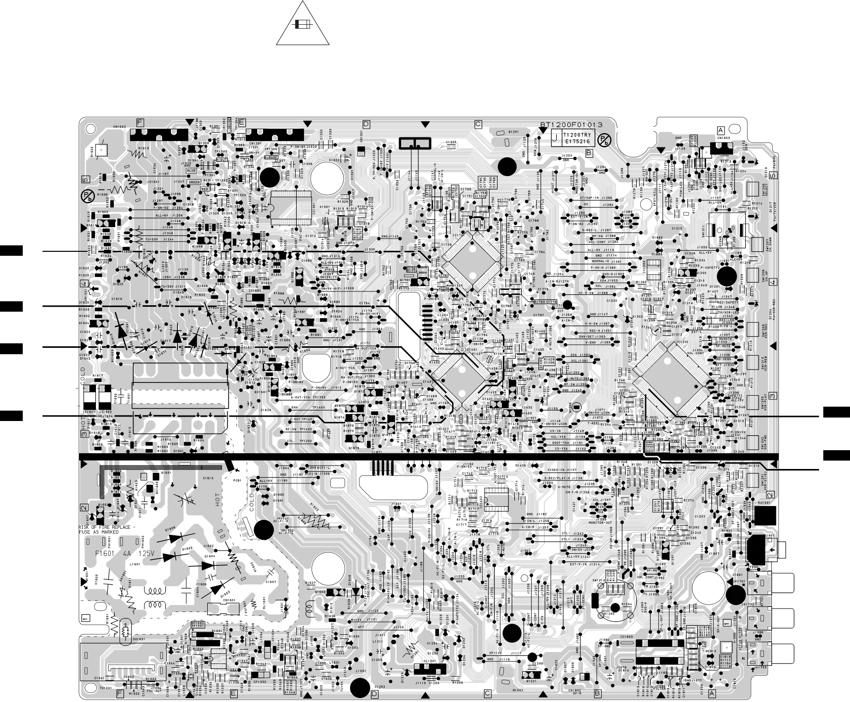
1-11-16
WF7
PIN 49
OF IC1401
PIN 32
OF IC1401
PIN 9
OF IC1401
WF8
WF4
WF2
PIN 10
OF IC1401
PIN 59
OF IC1201
WF16
WF15
PIN 58
OF IC1201
BT1200F01013
Main CBA Bottom View < TV/VCR Section >
Because a hot chassis ground is present in the power
supply circuit, an isolation transformer must be used.
Also, in order to have the ability to increase the input
slowly,when troubleshooting this type power supply
circuit, a variable isolation transformer is required.
NOTE:
The voltage for parts in hot circuit is measured using
hot GND as a common terminal.
For continued protection against risk of fire,
replace only with same type 4 A, 125V fuse.
CAUTION ! :
ATTENTION : Utiliser un fusible de rechange de même type de 4A, 125V.
4A 125V
CAUTION !
Fixed voltage (or Auto voltage selectable) power supply circuit is used in this unit.
If Main Fuse (F1601) is blown , check to see that all components in the power supply
circuit are not defective before you connect the AC plug to the AC power supply.
Otherwise it may cause some components in the power supply circuit to fail.
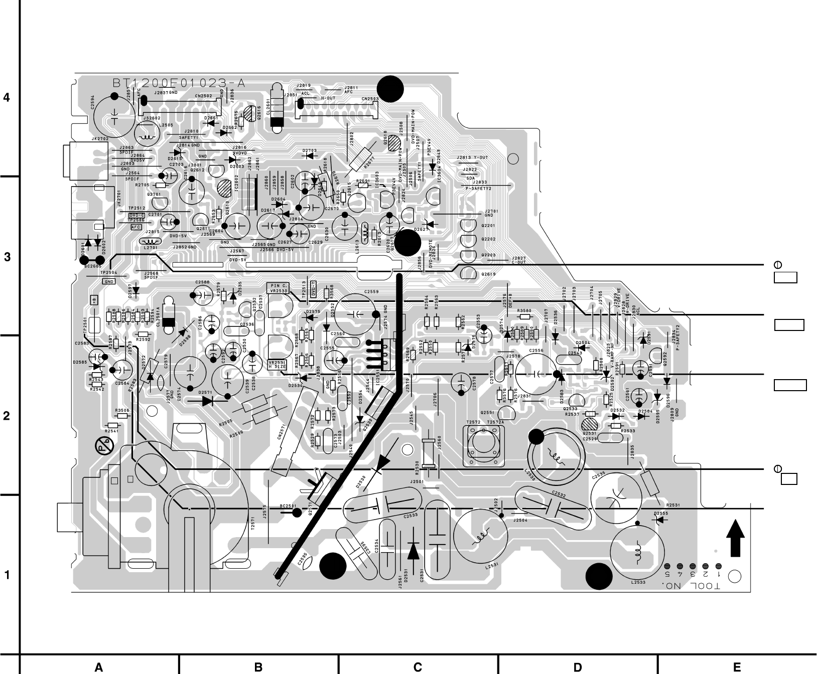
1-11-17
R2583
(H f0 Adjustment)
+B
TP2501
TP2504
GND
H SIZE
VR2531
PIN C.
VR2530
Sub CBA Top View < TV/VCR Section >
BT1200F01023-A
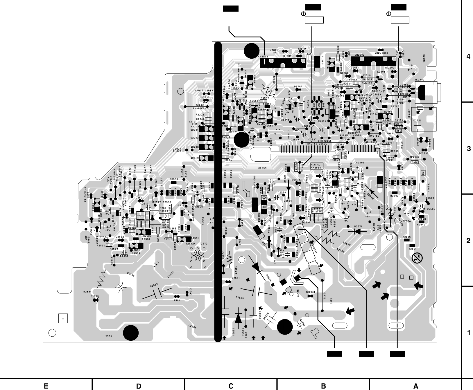
1-11-18
WF11
PIN 5
CN2571
Q2571
Collector
WF10
OF CN2503
PIN18
WF19
WF20
PIN2
OF CN2
DVD-Y
TP2513
WF17
DVD-C
TP2512
WF18
Sub CBA Bottom View < TV/VCR Section >
BT1200F01023-A
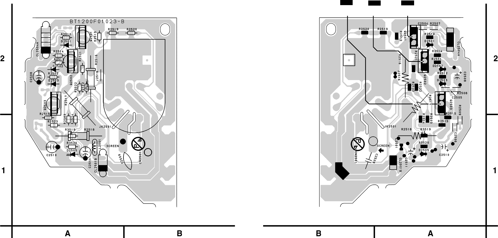
1-11-19
WF13
Q2502
Collector
WF12
Q2503
Collector
WF14
Q2501
Collector
CRT CBA Top View < TV/VCR Section > CRT CBA Bottom View < TV/VCR Section >
BT1200F01023-B
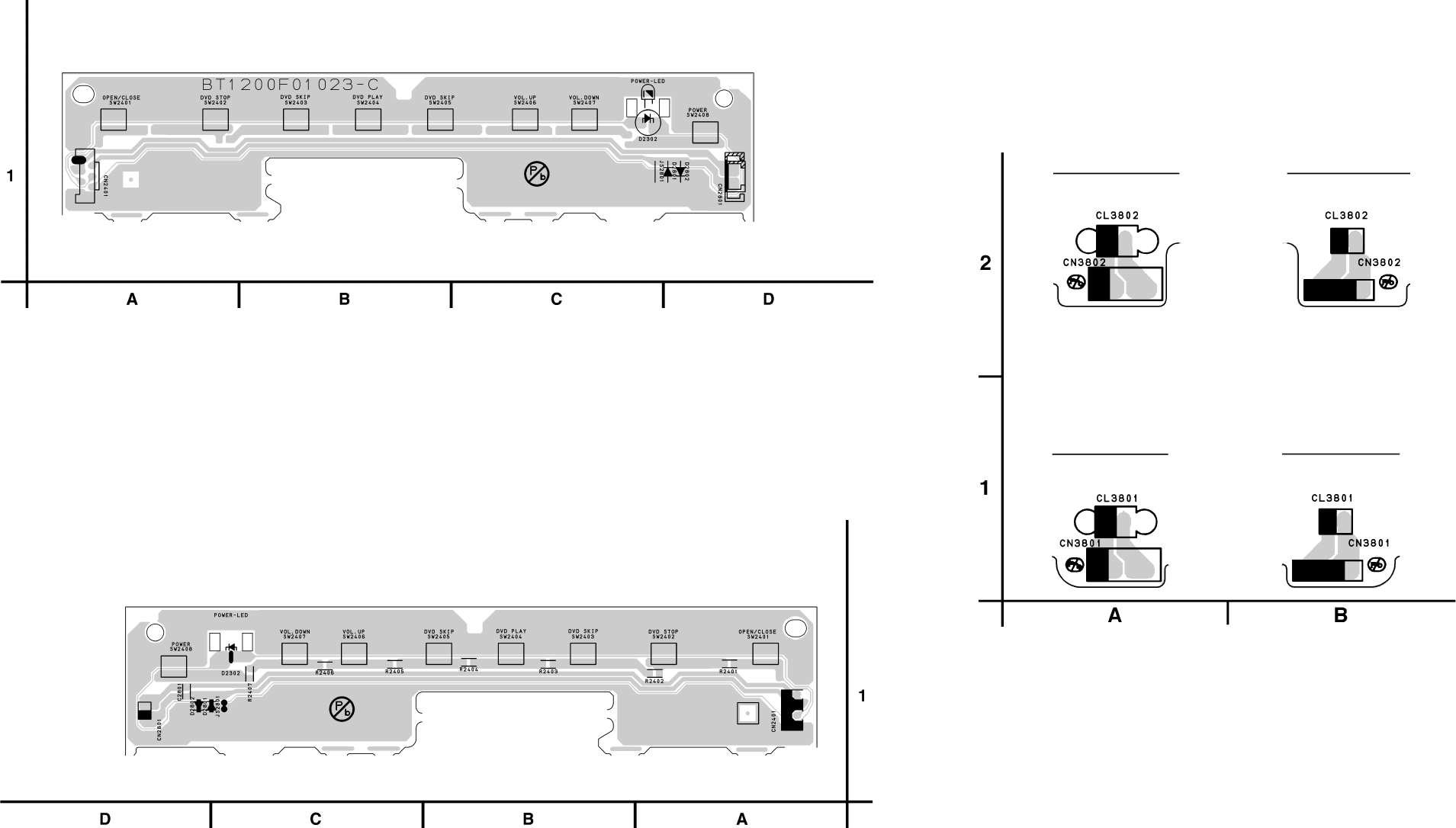
1-11-20
Function CBA Top View < TV/VCR Section >
Junction-B CBA
Top View
< TV/VCR Section >
BT1200F01023-C
Function CBA Bottom View < TV/VCR Section >
Junction-B CBA
Bottom View
< TV/VCR Section >
Junction-A CBA
Top View
< TV/VCR Section >
Junction-A CBA
Bottom View
< TV/VCR Section >
BT1200F01023-D
BT1200F01023-E
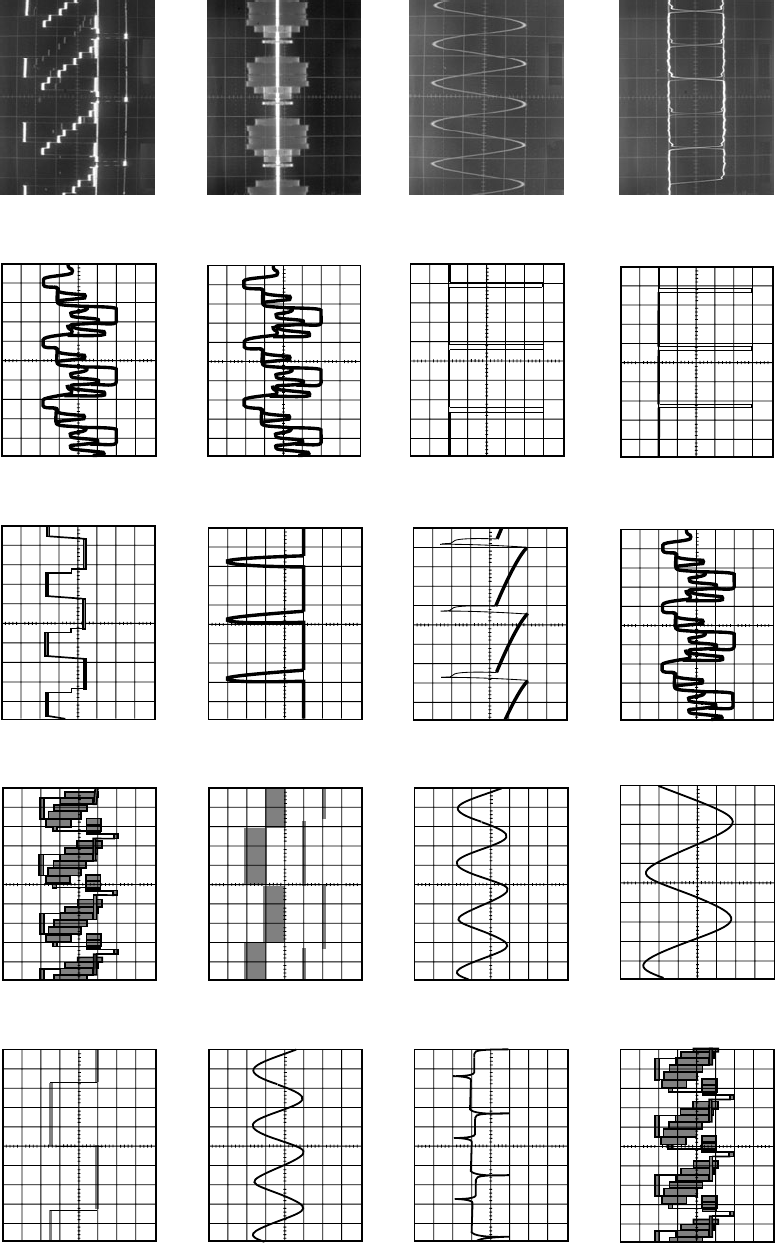
WAVEFORMS
X7TWF
1-12-1
WF2
WF1 WF5
WF4 WF8
WF7
WF3
WF9
WF11
WF13
WF14
WF10
WF15
WF16
WF12
WF18
WF17
WF19
WF20
SPDIF
SPDIF
1V 0.1
0.1
µ
sec
Input: NTSC Color Bar Signal (with 1kHz Audio Signal) --- WF1~WF16
DVD Video (Power on (Stop) MODE) --- WF17, WF18
CD (1KHz Play) --- WF19, WF20
INITIAL POSITION: Unplug unit from AC outlet for at least five minutes,
reconnect to AC outlet and then turn power on.
(Brightness---Center Color---Center Tint --- Center Contrast---Approx 70%)
1DIV: 2V 5ms
TP1402 RF-SW
1DIV: 0.2V 0.1µs
IC1401 Pin 49
1DIV: 1V 10ms
TP1202 CTL-AMP-OUT
1DIV: 0.25V 20 µs
IC1401 Pin 32
1DIV: 0.5V 20 µs
TP1401 V-OUT
Upper: WF6 Lower: WF1
1DIV: 0.2V 2DIV: 5V 5ms
TP1403 ENV.
1DIV: 0.5V 0.5ms
IC1401 PIN9
1DIV: 0.5V 0.5ms
IC1401 PIN10
1DIV: 2V 20µs
TP1305 H-OUT
1DIV: 200V 20µs
Q2571 COLLECTOR
1DIV: 10V 5ms
CN2571 PIN 5
1DIV: 20V 20µs
Q2503 COLLECTOR
1DIV: 20V 20µs
Q2502 COLLECTOR
1DIV: 20V 20µ
Q2501 COLLECTOR
1DIV: 1V 20µs
IC1201 PIN 58
1DIV: 1V 5ms
IC1201 PIN 59
1DIV: 0.2V 20µs
TP2513 DVD-Y
1DIV: 0.2V 20µs
TP2512 DVD-C
1DIV: 0.5V 0.5ms
CN2503 PIN 18
1DIV: 1V 0.1µs
CN2 PIN 1
s
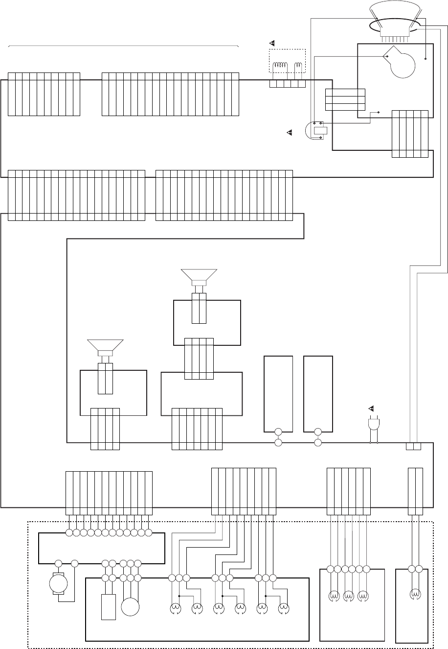
WIRING DIAGRAM < TV/VCR Section >
T2202WIT
1-13-1
1
2
CRT CBA
FOCUS
SCREEN
GND
L551
D.Y.
HD
VD
CL2501A
CL2501B
MAIN CBA
SUB CBA
CN2501
W1601
CN1601
1
2
3
4
5
T2571
FBT
CL2504A
ANODE
CN2571
FULL
ERASE HEAD
CL1403
FE HEAD
AUDIO HEAD
CONTROL
HEAD
ACE HEAD ASSEMBLY
AUDIO ERASE
HEAD
M
LOADING
MOTOR
CYLINDER
ASSEMBLY
1
CM+12V
P-ON+5V(3)
2
3
C-FG
CM-F/R
4
C-CONT
5
FG-GND
6
LD-CONT
7
D-CONT
8
D-PFG
9
M-GND
10
D/L+12V
11
VG+15V
12
CL1201
CL1401
CN1602 CN2502 CN2
CN1
CAPSTAN
MOTOR
Hi-Fi-
AUDIO(L)
HEAD
Hi-Fi-
AUDIO(R)
HEAD
VIDEO
(R)-2
HEAD
VIDEO
(L)-2
HEAD
VIDEO
(L)-1
HEAD
VIDEO
(R)-1
HEAD
CL1402
TO CN1A
TO CN2A
Hi-Fi-AUDIO(L)
9
Hi-Fi-COM
8
Hi-Fi-AUDIO(R)
7
VIDEO(R)-2
6
VIDEO-COM2
5
VIDEO(L)-2
4
VIDEO(L)-1
3
VIDEO-COM1
2
VIDEO(R)-1
1
AE-H
6
AE-H/FE-H
5
AUDIO-COM
4
AUDIO-PB/REC
3
CTL(+)
2
CTL(-)
1
FE-H
1
FE-H-GND
2
P-ON+8V(1)
1
RED
2
GREEN
3
BLUE
4
HEATER
11
GND
22
+180V
33
FUNCTION
CBA
CN2401CN1803
SP(L)
11
GND
22
SP(L)
33
NU
44
KEY1
55
NU
66
GND
77
DVD-AUDIO-MUTE
9
DVD-Y
8
GND
7
DVD-C
6
GND
5
DVD-AUDIO(L)
4
DVD-AUDIO(R)
3
GND
2
SPDIF
1
EV+1.2V
1
EV+1.2V
2
EV+1.2V
3
GND
4
GND
5
GND
6
GND
7
GND
8
PWRCON
15
EV+3.3V
9
EV+3.3V
10
DVD-ON+3.3V
11
DVD-ON+5V
12
EV+9V
14
EV+9V
13
GND
5
11+B
22+B
33GND
44GND
55GND
66+26V
77GND
88GND
99GND
10 10EV+4V
11 11EV+4V
12 12GND
13 13GND
14 14DVD-ON+9V
15 15GND
16 16P-ON+5V(4)
17 17P-SAFETY1
18 18P-SAFETY2
19 19DVD-REMOTE
CN1301 CN2503
11H-DRIVE
22ACL
33RED
44GREEN
55BLUE
66P-ON+8V(1)
99V-RAMP-NF
77AFC
88V-DRIVE
10 10DVD-Y
11 11DVD-C
12 12P-SAFETY3
13 13SDATA
14 14
SCLK
15 15
CS
16 16
DVD-AUDIO-MUTE
17 17
DVD-MAIN-POWER
18 18
DVD-AUDIO(L)
19 19
DVD-AUDIO(R)
SENSOR CBA
(ST-SENSOR)
SENSOR CBA
(END-SENSOR)
M
DRUM
MOTOR
PG
SENSOR
CONTINUE
WIRING DIAGRAM
<DVD SECTION>
WIRING DIAGRAM FOR
DECK MECHANISM SECTION
JUNCTION-A
CBA
SP1801
SPEAKER
R-CH
SP-GND
1SP(R)
2
CL3802
CN3802CN1802
SP(R)
11
SP(R)
22
SP-GND
33
SP-GND
44
JUNCTION-B
CBA
SP801
SPEAKER
L-CH
SP-GND
1SP(L)
2
CL3801
CN3801CN2801
SP(L)
11
SP(L)
22
SP-GND
33
SP-GND
44
DVD-ON+5V(NU)
10
DVD-REMOTE
19
SCLK
16
S D ATA
18
CS
17
1
2
3
4
5
CL2601
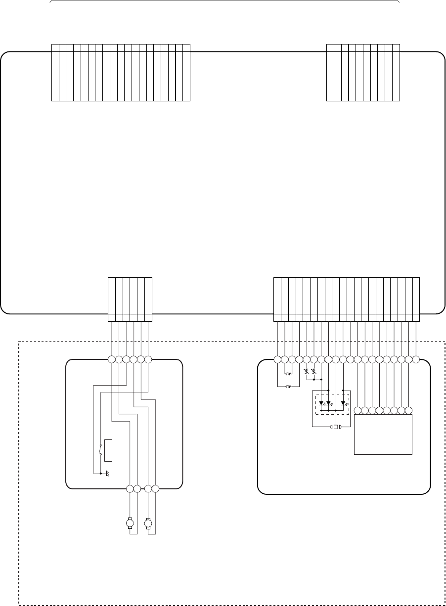
T2202WID
1-13-2
WIRING DIAGRAM < DVD Section >
DVD MAIN CBA UNIT
CONTINUE
WIRING DIAGRAM
<TV/VCR SECTION>
TO CN1
CN301
6
5
GND
SL(-)
SL(+)
4
3
SP(-)
2
SP(+)
1 TRAY-IN
TRAY-IN
DRIVE CBA
M
SLED
MOTOR
M
SPINDLE
MOTOR
EV+1.2V
EV+1.2V
EV+1.2V
GND
GND
GND
GND
1
2
3
4
5
6
7
GND
PWRCON
EV+3.3V
8
15
9
10
11
12
CN1A
PICK UP UNIT
CN201
1
2
3
4
5
6
7
8
9
10
11
12
13
14
15
16
17
18
19
20
TS(+)
TS(-)
FS(-)
CD-LD
FS(+)
GND(DVD-PD)
GND(CD-PD)
PD-MONI
DVD-LD
VREF
NU
GND
B
P-ON+5V
CD/DVD
D
A
C
NU
GND(LD)
DETECTOR
FSTS
7
9
11
2
3
6
5
4
TO CN2
SPDIF
GND
DVD-AUDIO(R)
DVD-AUDIO(L)
GND
1
2
3
4
5
CN2A
DVD-C
DVD-Y
GND
DVD-AUDIO-MUTE
6
7
8
9
EV+3.3V
DVD-ON+3.3V
DVD-ON+5V
EV+9V
14
13
EV+9V
DVD MECHANISM
DVD-ON+5V(NU)
10
16
17
SCLK
CS
S D ATA
19
18
DVD-REMOTE

1-14-1 X7T4HTI
SYSTEM CONTROL TIMING CHARTS
< TV/VCR Section >
Mode SW: LD-SW
Note: EJ RS: Loading FWD (LM-FWD / REV “H”)
RS EJ: Loading REV (LM-FWD / REV “L”)
Stop (A) = Loading
Stop (B) = Unloading
Note:
LD-SW Position detection
A/D Input voltage Limit
(Calculated voltage)
Symbol
3.76 V ~ 4.50 V (4.12 V) EJ
4.51 V ~ 5.00 V (5.00 V) CL
0.00 V ~ 0.25 V (0.00 V) SB
1.06 V ~ 1.50 V (1.21 V) TL
0.66 V ~ 1.05 V (0.91 V) FB
1.99 V ~ 2.60 V (2.17 V) SF
1.51 V ~ 1.98 V (1.80 V) SM
3.20 V ~ 3.75 V (3.40 V) AU
0.26 V ~ 0.65 V (0.44 V) AL
4.51 V ~ 5.00 V (5.00 V) SS
2.61 V ~ 3.19 V (2.97 V) RS
Note:
Symbol Loading Status
EJ Eject
CL Eject ~ REW Reel
SB REW Reel ~ Stop (B)
TL Stop (B) ~ Brake Cancel
FB Brake Cancel ~ FF / REW
SF FF / REW ~ Stop (M), (FF / REW)
SM Stop (M), (FF / REW) ~ Stop (A)
AU Stop (A) ~ Play / REC
AL Play / REC ~ Still / Slow
SS Still / Slow ~ RS (REW Search)
RS RS (REW Search)
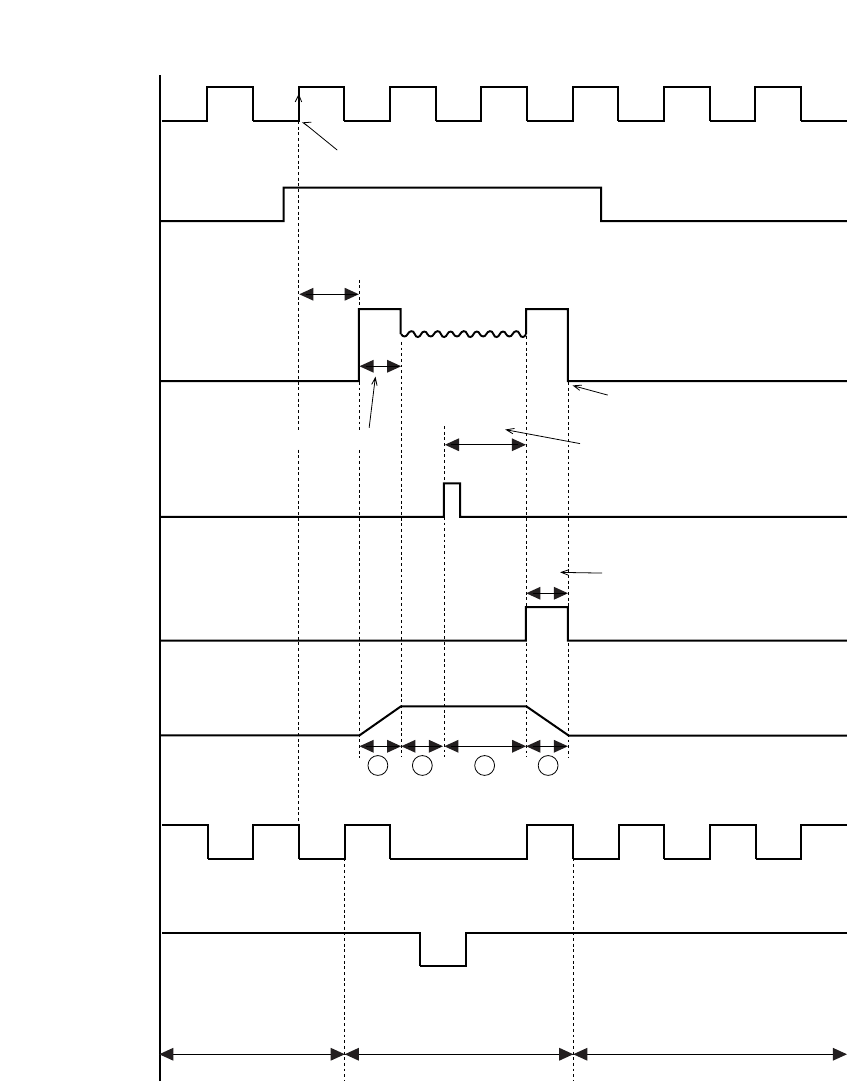
1-14-2 X7T4HTI
Chart 1
18 RF-SW
F-AD
( Internal Signal )
C-DRIVE
PB CTL
66 C-F/R
STILL STILLFRAME ADVANCE
ROLL
COMPENSATION
(DRUM SERVO)
H-A-SW
15 ROTA
AT
The first rise of RF-SW after a rise in F-AD signal.
ST
T1
BL
"H" "H"
T2
"Z"
1) SP MODE
12 3 4
Acceleration Detection
Stop Detection
Slow Tracking Value
Reversal Limit Value
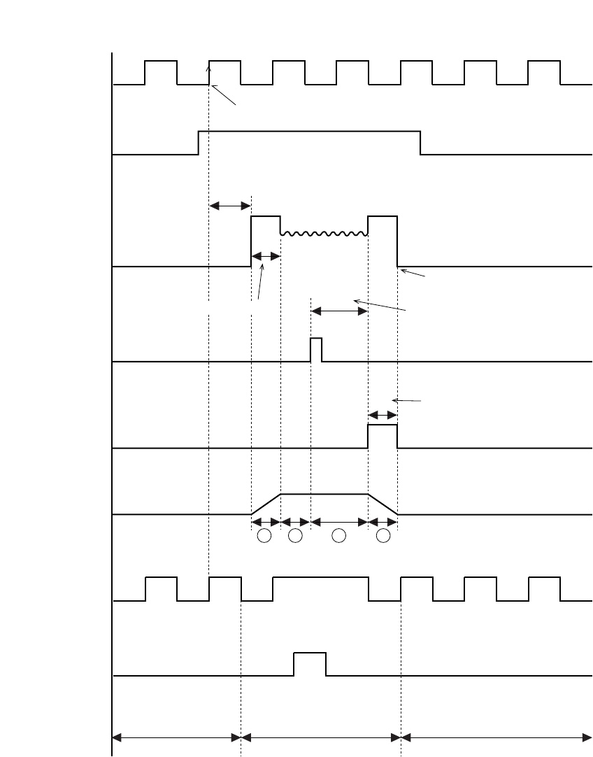
1-14-3 X7T4HTI
Chart 2
18 RF-SW
F-AD
( Internal Signal )
C-DRIVE
PB CTL
66 C-F/R
STILL STILLFRAME ADVANCE
ROLL
COMPENSATION
(DRUM SERVO)
H-A-SW
15 ROTA
AT
The first rise of RF-SW after a rise in F-AD signal.
ST
T1
BL
"H" "H"
T2
"Z"
2) LP/EP MODE
12 3 4
Acceleration Detection
Stop Detection
Slow Tracking Value
Reversal Limit Value
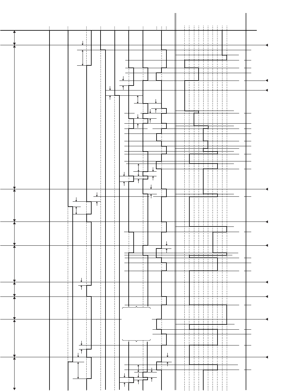
1-14-4 X7T4HTI
Chart 3
+100mS(NTSC)
+620mS(PAL)
1. EJECT (POWER OFF) -> CASSETTE IN (POWER ON) -> STOP(B) -> STOP(A) -> PLAY -> RS -> FS -> PLAY -> STILL/SLOW -> PLAY -> STOP(A)
EJECT
CASS.LOAD
ST-S/
END-S
"OFF"
PLAY
REW
FF
PLAY
PLAY
STOP
/EJECT
0.2S
0.4S
0.2S
LD-FWD
STOP(A)
STOP(A)
LD-FWD
LD-REV
0.2S
LD-FWD
LD-FWD
LD-FWD
LD-FWD
LD-FWD
STILL(SLOW)
RS1(RS2)
FS1(FS2)
PLAY
PLAY
PLAY
0.2S
LD-REV
LD-REV
LD-FWD
LD-REV
LD-REV
LD-REV
0.2S
0.5S
CLEJ SS
SS
AU AU
TL
"Z"
ON
ON
PAUSE
(SLOW)
AU AL AL AU
SF
SM
POWER
-OFF
STOP PLAY RS FS
STILL
(SLOW)
PLAY STOPPLAY
SB TL SB FB SM SMSF AL AL RS AU AL SS AU AL SM
0.8S
0.2S
0.3S
1.0S
0.2S 0.5S 0.12S 1.2S
0.2S
1.2S 0.2S 20mS
0.4S
40mS
0.2S
0.2S
Refer to STILL/
SLOW TIMING
CHART 1, 2.
0.3S
0.2S
20mS
40mS
0.4S
0.2S
0.2S
0.2S
0.3S
REC
SFT-SW
POWER
STOP(B)
PIN NO.
LD-SW
CL/SS
LD-CONT
C-DRIVE
C-F/R
DRUM
ROTATION
P-ON-H
AUDIO-MUTE
D-REC-H
D-PB-H
EJ
AU
RS
SF
SM
TL
FB
AL
SB
1
82
66
31
65
44
DISPLAY
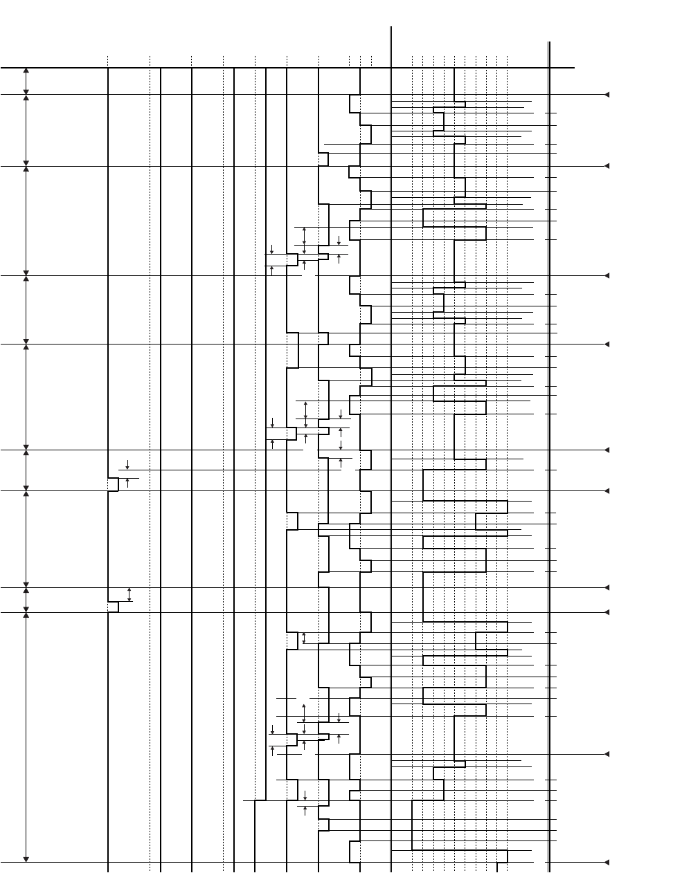
1-14-5 X7T4HTI
Chart 4
PIN NO.
LD-SW
CL/SS
LD-CONT
C-DRIVE
"Z"
ON
ON
C-F/R
DRUM
ROTATION
P-ON-H
AUDIO-MUTE
D-REC-H
D-PB-H
EJ
AU
RS
SF
SM
TL
FB
AL
SB
1
82
66
31
65
44
DISPLAY
ST-S
"ON"
REC
REW
FF
STOP
/EJECT
0.5S
1.0S
0.2S
0.2S
0.5S
0.2S
0.5S
0.5S
0.5S
0.2S
0.2S
0.2S
1.5S
2.5S Short REV
1.0S
0.2S
0.2S
LD-FWD
REV
LD-FWD
STOP(A)
STOP(A)
STOP(A)
CASS. UNLD
EJECT
STOP(A)
LD-REV
FF
LD-REV
LD-REV
LD-FWD
LD-FWD
LD-FWD
LD-FWD
LD-FWD
LD-FWD
LD-FWD
REC PAUSE
REC
REC
REW
LD-REV
LD-REV
LD-REV
LD-REV
LD-REV
LD-REV
LD-REV
PAUSE
REC or
PAUSE
STOP
/EJECT
STOP
/EJECT
STOP
/EJECT
2. STOP(A) -> FF -> STOP(A) -> REW -> STOP(A) -> REC -> PAUSE -> PAUSE or REC -> STOP(A) -> EJECT
STOPFF
STOP
REW STOP REC RECREC PAUSE STOP
TL TL SMSM SF SFAL AL SM AL AL ALAU AU SM TL SB EJRS RSSM
SM SF FB SM AU AU SS
SS SS SF
AU AL AL AUSS FB CL
SF FB SM
FB SF AU AUFB SF
1.0S 1.2S
0.2S
40mS
0.4S
0.2S
0.4S
20mS
40mS
0.2S
20mS
0.2S
0.4S
1.5S(NTSC)
1.0S(PAL)
40mS
20mS 0.1S
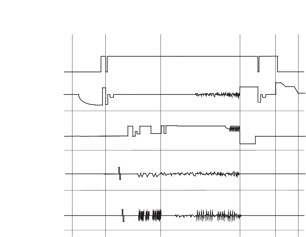
1-14-6 X7T4HTI
< DVD Section >
Tray IN
(TL221)
Sled Drive
(TP303)
Disc Drive
(TP301)
Focus Drive
(TP304)
Tracking Drive
(TP302)
0V
3.3V
0V
1.65V
0V
0V
0V
1.65V
1.65V
1.65V
Tray Close ~ Play / Play ~ Tray Open
Tray
Close
Disc
Rotation Play Disc
Stop
Tray
Open

1-15-1 T2203PIN
IC PIN FUNCTION DESCRIPTIONS
IC1201 (TV/VCR Micro Controller IC)
“H” ≥ 4.5 V, “L” ≤ 1.0 V
Pin
No.
IN/
OUT
Signal
Name Function
1 IN LD-SW Loading Switch Input
2 OUT DVD-LED DVD LED Control Output
3IN
P-SAFETY
2Power Supply Failure
Detection 2
4 IN ST/SAP-IN Tuner Stereo/Sap Detector
Signal Input
5 IN KEY0 Key Input 0
6 IN KEY1 Key Input 1
7 IN END-SENS End-Sensor
8 IN AFT AFT Voltage Input
9 IN ST-SENS Start-Sensor
10 IN V-ENV Video Envelope Input
11 OUT VOLUME Volume Control Signal
Output
12 OUT SP-MUTE Speaker Mute Signal Output
13 OUT DV-SYNC Artificial Vertical Sync Output
14 IN REMOTE Remote Control Signal Input
15 OUT ROTA Color Phase Rotary
Changeover Signal
16 OUT V-H-SW Video Head Amp Switching
Pulse
17 IN ENV-DET Envelope Comparator Signal
18 OUT RF-SW Video Head Switching Pulse
19 OUT Hi-Fi-H-SW HiFi Audio Head Switching
Pulse
20 - NU Not Used
21 OUT REC-LED REC LED Control Signal
22 IN NORMAL-
HAudio Mode Input Signal
23 - NU Not Used
24 - NU Not Used
25 OUT DVD-
REMOTE Remote Control Signal
Output to DVD
26 OUT TV/VCR-
LED TV/VCR LED Control Signal
27 - NU Not Used
28 - NU Not Used
29 OUT D-REC
/PB-L Delayed Record/Playback
Control Signal
30 - NU Not Used
31 OUT P-ON-H Power On Signal at High
32 - NU Not Used
33 IN REC-
SAFETY Record Protection Tab
Detection
34 IN RESET System Reset Signal (Reset
= “L”)
35 IN XC-IN Sub Clock (32kHz)
36 OUT XC-OUT Sub Clock (32kHz)
37 - TIMER+5V Vcc
38 IN X-IN Main Clock (10.6MHz)
39 OUT X-OUT Main Clock (10.6MHz)
40 - GND GND
41 OUT SPOT-KILL Counter Measure for Spot
42 IN DVD-MAIN-
POWER Power On Signal at High for
DVD
43 IN CLKSEL Clock Select (GND)
44 OUT D-REC-H Delayed Record Control
Signal
45 IN I2C-OPEN Chip Select
46 - GND GND
47 IN DVD-
AUDIO-
MUTE DVD Audio Mute Signal
48 OUT DVD-H DVD at High
49 - GND GND
50 IN CS DVD Interface Chip Select
51 IN SCLK DVD Interface Serial Clock
52 IN SDATA DVD Interface Serial Data
53 - P-ON+5V OSD Vcc
54 - HLF Horizontal Filter
55 IN V-HOLD Vertical Hold
56 IN CV-IN Composite Video Signal
Input
57 - GND GND
58 IN H-SYNC Horizontal SYNC Input
59 IN V-SYNC Vertical SYNC Input
60 OUT OSD-BLK Output for Picture Cut off
61 OUT DG-ON-H Degaussing Coil Control
Signal
62 OUT OSD-B Blue Signal Output
63 OUT OSD-G Green Signal Output
64 OUT OSD-R Red Signal Output
65 OUT AUDIO-
MUTE Audio Mute Signal Output
Pin
No.
IN/
OUT
Signal
Name Function

1-15-2 T2203PIN
66 OUT C-F/R Capstan Motor FWD/REV
Control Signal
67 OUT D-REC
/PB-H Delayed Record/Playback
Control Signal
68 OUT YCA-SDA YCA Serial Data
69 OUT YCA-CS YCA Chip Select
70 OUT YCA-SCL YCA Serial Clock
71 OUT SCL Serial Clock
72 IN/
OUT SDA Serial Data
73 - NU Not Used
74 IN C-SYNC Composite Sync Input
75 - NU Not Used
76 OUT C-CONT Capstan Motor Control
Signal
77 OUT D-CONT Drum Motor Control Signal
78 IN P-SAFETY
3Power Supply Failure
Detection 3
79 - NU Not Used
80 IN T-REEL Take Up Reel Rotation
Signal
81 - NU Not Used
82 OUT LD-CONT Loading Motor Control Signal
83 - NU Not Used
84 IN P-DOWN Power Voltage Down
Detector Signal
85 - NU Not Used
86 - NU Not Used
87 IN C-FG Capstan Motor Rotation
Detection Pulse
88 - GND GND (AMP)
89 - NU Not Used
90 IN D-PFG Drum Motor Pulse Generator
91 - NU Not Used
92 IN AMP-
VREF-IN Standard Voltage Input
93 - C Ext. Capacitor Connection
Port for Analog Amp
94 IN/
OUT CTL (-) Record/Playback Control
Signal (-)
95 IN/
OUT CTL (+) Record/Playback Control
Signal (+)
96 - AMPC Amp Capacitor
97 OUT CTL-AMP-
OUT Control Amp Output
98 - P-ON+5V Power Supply for AMP
Pin
No.
IN/
OUT
Signal
Name Function
99 - AL+5V A/D, D/A Standard Voltage
100 IN P-SAFETY
1Power Supply Failure
Detection 1
Pin
No.
IN/
OUT
Signal
Name Function
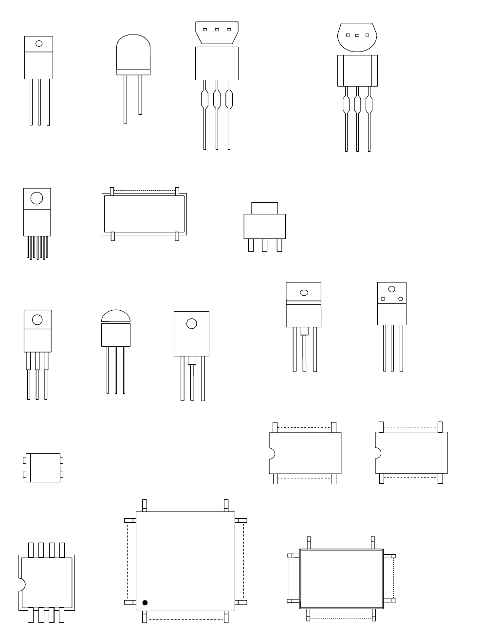
1-16-1 T2202LE
LEAD IDENTIFICATIONS
80 51
81
100
130
50
31
5
4
8
1
E
C
60
21
40
41
20
1
80
61
42 22
21
1
20 11
10
1
S D G
16
9
1
8
17
1
2
4
3
1: A
2: K
3: E
4: C
123
1: R
2: A
3: K
ECB ECB
123
1: GND
2: Vout
3: Vin
B C E B C E
ECB
KIA7805API/P
LTV-817C-F
M3776AMCH-BA4GP
CAT24WC02WI-TE13
MID-32A22F
LA71205M-MPB-E
LA72670BM-MPB-E
KIA431-AT/P
M61275FP-TF3H
M61116FP TF0G
KTC3503-Y/P
2SK3561
AN17812A
Note:
A: Anode
K: Cathode
E: Emitter
C: Collector
B: Base
R: Reference
S: Source
G: Gate
D: Drain
LA78041-E
1: IN
2: GND
3: OUT
123
2SC2785(F)
KRA103M-AT/P
KRC103M-AT/P
KTC3199-GR-AT/P
KTC3199-Y-AT/P
KTC3205-Y-AT/P
2SA1175(F)
2SA950-O(TE2 F T)
2SC2120-O(TE2 F T)
2SC1627-Y(TE2.F.T)
2SC3331(T)
2SC3708S
TLV1117IDCYRG3
2SC5978 2SD1666R
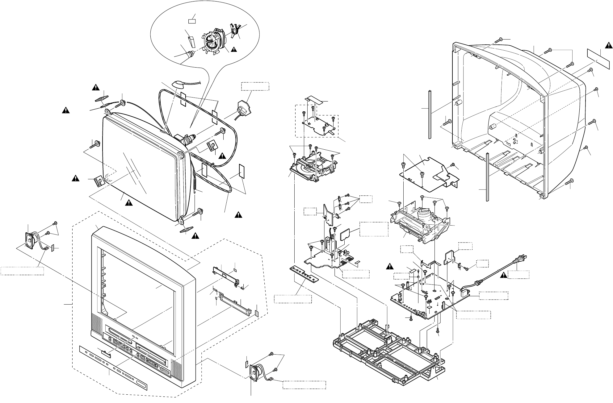
1-17-1 T2202CEX
EXPLODED VIEWS
Cabinet
V501-1
L551
Details for L551
and surrounding parts
SHINWHA
TAPE SGT-730
(WHITE)
SHINWHA
TAPE SGT-730
(BLACK)
V501-2
CRT CBA
DVD Main
CBA Unit
Sub CBA
Function CBA Main CBA
W1601
1B1
1B2
DG601
Scotch
Tape #880
Scotch
Tape #880
Scotch
Tape #880
Sensor CBA
CLN551CLN551CLN551
V501
TB1
TB17
TL18
TB13
TB3
TL1-3
TL14
TL1-1
TL1-1
TL4
TL4
L1
L1
L1
L1
A2 A3
L1
L3-2
L3-1
TL1-1
TL1-2
TL1-2
DL2
DB2
TL1-2
TL1-3
B5
B5
L2
B2
B2
B2
B2
B4
B4
B4
B4
B1
A1-7 A1-9
A1-8
A1-5
A1-6
A1-4
A1-3
A1-1
A1-2
B7
TL3
TL3
TB2
TB18
TB19 TL6
TL1-3
A1X
L4
B6
Junction-A CBA
SP1801
L4
B6
SP801
Junction-B CBA
DVD Mechanical Parts
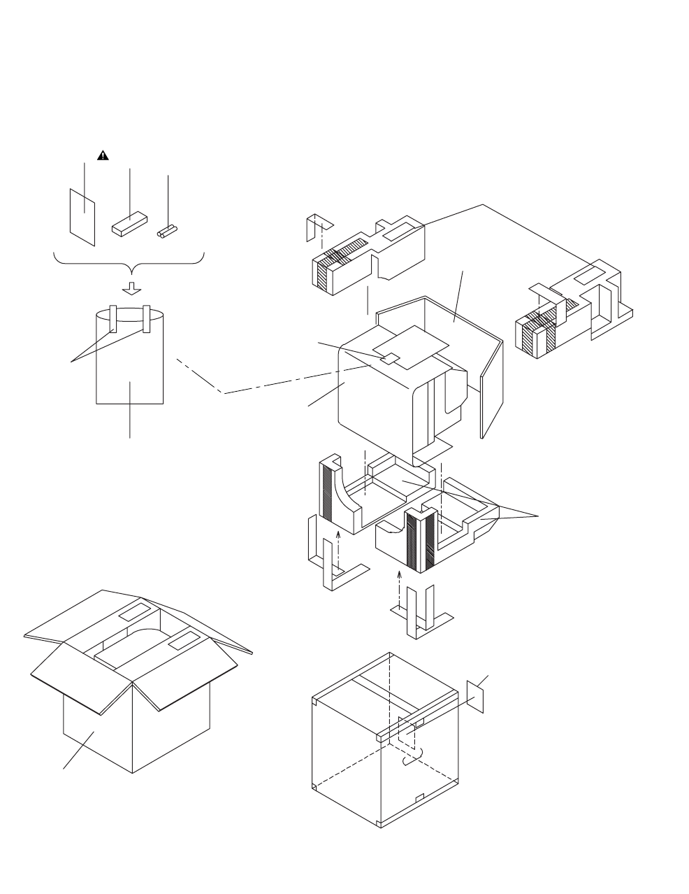
1-17-2 T2203PEX
Packing
FRONT
S4
S1
X1
Tape
X4
X2 X3
S3
S6
S7
S2
Packing Tape
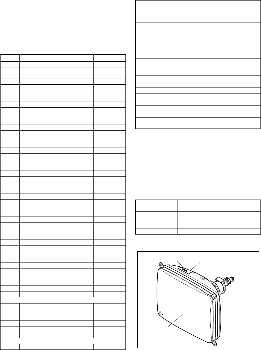
20060325 1-18-1 T2202CA
MECHANICAL PARTS LIST
PRODUCT SAFETY NOTE: Products marked with a
# have special characteristics important to safety.
Before replacing any of these components, read
carefully the product safety notice in this service
manual. Don't degrade the safety of the product
through improper servicing.
NOTE: Parts that are not assigned part numbers
(---------) are not available.
Table 1 (V501 and L551 Combination)
Note 1: Purity and Convergence Adjustments must be
performed following CRT replacement. Refer to
Electrical Adjustment Instructions.
Note 2: Please confirm CRT Type No. on the CRT
Warning Label which is located on the CRT. Then See
the Table 1 for V501 and L551 combination chart.
Please refer this CRT, Deflection Yoke combination
chart for parts order.
CRT Warning Label Location
Ref. No. Description Part No.
A1X FRONT CABINET ASSEMBLY T2202UC 1EM121336
A1-1 FRONT CABINET T2202UC 1EM121337
A1-2 CONTROL PLATE T2202UC 1EM221102
A1-3 BADGE BRAND T7310UL ~MAGNAVOX~ 0EM407275
A1-4 CASSETTE DOOR T2100UA 1EM320170A
A1-5 SPRING DOOR T1200UA 1EM422903
A1-6 CLOTH(4X7XT0.7) T5000UA 0EM404974
A1-7 TRAY PANEL T2100UA 1EM320169
A1-8 TRAY SPRING TD707UH 0EM408552
A1-9 CLOTH(10X20XT 0.3) T2100UA 1EM421154
A2 REAR CABINETT T2200UA 1EM020688
A3#RATING LABEL T2202UC ----------
1B1 DECK ASSEMBLY CZD014/VM2466 N2466FT
1B2 DVD MECHA X7 TRIPLE N79U1KVM N79U1KVM
B1 SPRING TENSION B0080B0 EM40808 26WH006
B2 SCREW M7 CRT(D22) T7205UF 0EM406573A
B4#HOLDER DEGAUSS L1200UA 0EM405869
B5 CLOTH 190X15XT0.5 TS7623
B6 CLOTH(10X30XT0.5) B5900UA 0EM404486
B7 CLOTH(15X10XT0.5) L9700UA 0EM405038
CLN551#WIRE CRT GND WX1L6240-005 WX1L6240-005
DG601#DEGAUSSING COIL LLBH00ZTM048 LLBH00ZTM048
L1 SCREW P-TIGHT 4X18 BIND HEAD + GBJP4180
L2 SCREW TAPPING M4X14 DBT14140
L3-1 SCREW P-TIGHT 3X10 BIND HEAD+ GBHP3100
L3-2 SCREW P-TIGHT 3X10 BIND HEAD+ GBHP3100
L4 SCREW P-TIGHT 3X10 BIND HEAD+ GBJP3100
SP801 SPEAKER S0407F01A DSD0807XQ001
SP1801 SPEAKER S0407F01A DSD0807XQ001
TB1 TRAY CHASSIS T1200UA 1EM020548
TB2 TOP SHIELD T5500UA 0EM201787
TB18 LASER CAUTION LABEL T8200UA ----------
TB19#24V CHASSIS NO. LABEL TJ T2200UA ----------
TL1-1 SCREW P-TIGHT 3X12 WASHER HEAD+ GCJP3120
TL1-2 SCREW P-TIGHT 3X12 WASHER HEAD+ GCJP3120
TL1-3 SCREW P-TIGHT 3X12 WASHER HEAD+ GCJP3120
TL3 SCREW S-TIGHT M3X4 BIND HEAD GBJS3040
TL4 SCREW P-TIGHT 3X20 BIND HEAD + GBJP3200
TL14 SCREW B-TIGHT D3X8 BIND HEAD+ GBJB3080
TL18 SCREW P-TIGHT M3X8 BIND HEAD+ BLK GBHP3080
V501-2 WEDGE FT-00110W XV10000T4001
PACKING
S1 CARTON T2202UC 1EM423156
S2 STYROFOAM TOP T2200UA 1EM020890
S3 STYROFOAM BOTTOM T2200UA 1EM020891
S4 SERIAL NO. LABEL T2202UC ----------
S6 SHEET SET PCEC 003502019816 0EM403887
S7 HOLD PAD T2200UA 1EM423082
ACCESSORIES
X1 BAG POLYETHYLENE 235X365XT0.03 0EM408420A
X2#OWNERS MANUAL T2202UC 1EMN21690
X3 REMOTE CONTROL NF104UD 151/ECNX701/
NF104UD NF104UD
X4 DRY BATTERY(SUNRISE) R6SSE/2S XB0M451MS002
Note:
1. V501 (CRT) HAS COUPLE OF SUBSTITUTIONAL PARTS AND EACH PARTS
ALSO HAS MATCHING COMBINATION WITH L551.
PLEASE SEE TABLE 1 FOR DETAILS OF MATCHING COMBINATION.
2. L551 (DEFLECTION YOKE) HAS MATCHING COMBINATION WITH V501.
PLEASE SEE TABLE 1 FOR DETAILS OF MATCHING COMBINATION.
CRT TYPE A
L551#DEFLECTION YOKE CDY-F2518F LLBY00ZQS016
V501#CRT A59KPR84X TCRT190SM029
V501-1 PCM JH88DTA XM04000BV010
CRT TYPE B
L551#DEFLECTION YOKE 6150Z-1030X LLBY00ZGS007
V501#CRT A59KYL220X TCRT190GS040
V501-1 PCM JH88DTA XM04000BV010
CRT TYPE C
V501#CRT A59KPR84X01 S TCRT190SM037
CRT TYPE D
V501#CRT(BARE+DY) A59ELN011X007 TCRT190TMS01
V501-1 PCM JH88DTA XM04000BV010
V501: CRT Type No. V501: CRT Part No. L551: Deflection
Yoke Part No.
A59KPR84X TCRT190SM029 LLBY00ZQS016
A59KYL220X TCRT190GS040 LLBY00ZGS007
A59KPR84X01 S TCRT190SM037 --------------------
A59ELN011X007 TCRT190TMS01 --------------------
Ref. No. Description Part No.
CRT
CRT Warning Label
CRT Type No.
20060325 1-19-1 T2202EL
ELECTRICAL PARTS LIST
PRODUCT SAFETY NOTE: Products marked with a
# have special characteristics important to safety.
Before replacing any of these components, read
carefully the product safety notice in this service
manual. Don't degrade the safety of the product
through improper servicing.
NOTES:
1. Parts that are not assigned part numbers (---------)
are not available.
2. Tolerance of Capacitors and Resistors are noted
with the following symbols.
DVD MAIN CBA UNIT
MMA CBA
MAIN CBA
C.....±0.25% D.....±0.5% F.....±1%
G.....±2% J......±5% K.....±10%
M.....±20% N.....±30% Z.....+80/-20%
Ref. No. Description Part No.
DVD MAIN CBA UNIT N79T1KUP
Ref. No. Description Part No.
MMA CBA
Consists of the following: 1ESA12613
MAIN CBA
SENSOR CBA ----------
1ESA12193
Ref. No. Description Part No.
MAIN CBA
Consists of the following: ----------
CAPACITORS
C1004 CHIP CERAMIC CAP. F Z 0.01µF/50V CHD1JZ30F103
C1008 ELECTROLYTIC CAP. 10µF/50V M H7 CE1JMAVSL100
C1030 ELECTROLYTIC CAP. 100µF/10V M CE1AMASDL101
C1034 CHIP CERAMIC CAP.(1608) B K 1000pF/50V CHD1JK30B102
C1035 CHIP CERAMIC CAP. F Z 1µF/10V CHD1AZ30F105
C1036 CHIP CERAMIC CAP. CH J 120pF/50V CHD1JJ3CH121
C1037 CHIP CERAMIC CAP. F Z 0.01µF/50V CHD1JZ30F103
C1040 CHIP CERAMIC CAP.(1608) B K 0.01µF/50V CHD1JK30B103
C1043 FILM CAP.(P) 0.018µF/50V J CMA1JJS00183
C1044 CHIP CERAMIC CAP.(1608) B K 0.047µF/50V CHD1JK30B473
C1045 CHIP CERAMIC CAP. CJ C 3.3pF/50V CHD1JC3CJ3R3
C1046 ELECTROLYTIC CAP. 1µF/50V M H7 CE1JMAVSL1R0
C1048 ELECTROLYTIC CAP. 4.7µF/50V M H7 CE1JMAVSL4R7
C1049 CERAMIC CAP.(AX) CH K 2.7pF/50V CCA1JKTCH2R7
C1050 CHIP CERAMIC CAP.(1608) CH D 5.6pF/50V CHD1JD3CH5R6
C1117 CHIP CERAMIC CAP.(1608) B K 6800pF/50V CHD1JK30B682
C1118 CHIP CERAMIC CAP.(1608) B K 6800pF/50V CHD1JK30B682
C1203 CHIP CERAMIC CAP.(1608) F Z 0.1µF/50V CHD1JZ30F104
C1206 CHIP CERAMIC CAP. B K 0.056µF/50V CHD1JK30B563
C1207 ELECTROLYTIC CAP. 47µF/6.3V M H7 CE0KMAVSL470
C1208 ELECTROLYTIC CAP. 47µF/6.3V M H7 CE0KMAVSL470
C1210 CHIP CERAMIC CAP. F Z 1µF/10V CHD1AZ30F105
C1212 CHIP CERAMIC CAP.(1608) CH J 22pF/50V CHD1JJ3CH220
C1213 CHIP CERAMIC CAP.(1608) CH J 22pF/50V CHD1JJ3CH220
C1214 ELECTROLYTIC CAP. 47µF/6.3V M H7 CE0KMAVSL470
C1217 CHIP CERAMIC CAP.(1608) CH D 10pF/50V CHD1JD3CH100
C1218 CHIP CERAMIC CAP. CH J 15pF/50V CHD1JJ3CH150
C1222 CHIP CERAMIC CAP. B K 2200pF/50V CHD1JK30B222
C1223 CHIP CERAMIC CAP. F Z 1µF/10V CHD1AZ30F105
C1224 CHIP CERAMIC CAP.(1608) B K 1000pF/50V CHD1JK30B102
C1225 CHIP CERAMIC CAP. CH J 560pF/50V CHD1JJ3CH561
C1227 CHIP CERAMIC CAP.(1608) CH J 100pF/50V CHD1JJ3CH101
C1228 CHIP CERAMIC CAP.(1608) CH J 100pF/50V CHD1JJ3CH101
C1234 CHIP CERAMIC CAP.(1608) F Z 0.1µF/25V CHD1EZ30F104
C1235 CHIP CERAMIC CAP.(1608) B K 0.022µF/50V CHD1JK30B223
C1239 ELECTROLYTIC CAP. 22µF/16V M H7 CE1CMAVSL220
C1240 CHIP CERAMIC CAP. CH J 560pF/50V CHD1JJ3CH561
C1241 CHIP CERAMIC CAP.(1608) B K 4700pF/50V CHD1JK30B472
C1242 CHIP CERAMIC CAP.(1608) B K 1000pF/50V CHD1JK30B102
C1243 ELECTROLYTIC CAP. 22µF/16V M LL CE1CMASLH220
C1245 ELECTROLYTIC CAP. 47µF/6.3V M H7 CE0KMAVSL470
C1247 ELECTROLYTIC CAP. 47µF/6.3V M H7 CE0KMAVSL470
C1251 CHIP CERAMIC CAP.(1608) B K 2700pF/50V CHD1JK30B272
C1252 ELECTROLYTIC CAP. 100µF/16V M CE1CMASDL101
C1253 ELECTROLYTIC CAP. 100µF/10V M CE1AMASDL101
C1254 ELECTROLYTIC CAP. 47µF/25V M CE1EMASDL470
C1264 CHIP CERAMIC CAP. F Z 0.047µF/50V CHD1JZ30F473
C1299 ELECTROLYTIC CAP. 4.7µF/50V M H7 CE1JMAVSL4R7
C1309 CHIP CERAMIC CAP. F Z 1µF/10V CHD1AZ30F105
C1312 CHIP CERAMIC CAP.(1608) CH J 100pF/50V CHD1JJ3CH101
C1313 CHIP CERAMIC CAP.(1608) CH J 100pF/50V CHD1JJ3CH101
C1314 CHIP CERAMIC CAP.(1608) B K 0.01µF/50V CHD1JK30B103
C1316 ELECTROLYTIC CAP. 0.47µF/50V M H7 CE1JMAVSLR47
C1317 CHIP CERAMIC CAP.(1608) F Z 0.1µF/25V CHD1EZ30F104
C1319 CHIP CERAMIC CAP. F Z 1µF/10V CHD1AZ30F105
C1321 ELECTROLYTIC CAP. 100µF/10V M CE1AMASDL101
C1323 CHIP CERAMIC CAP. F Z 1µF/10V CHD1AZ30F105
C1325 CHIP CERAMIC CAP. F Z 1µF/10V CHD1AZ30F105
C1332 CHIP CERAMIC CAP. F Z 1µF/10V CHD1AZ30F105
C1333 CHIP CERAMIC CAP.(1608) F Z 0.1µF/50V CHD1JZ30F104
C1336 STACKED FILM CAP. 0.47µF/50V J CMA1JJS00474
C1337 CHIP CERAMIC CAP.(1608) B K 0.01µF/50V CHD1JK30B103
C1338 CHIP CERAMIC CAP. F Z 1µF/10V CHD1AZ30F105
C1339 CHIP CERAMIC CAP.(1608) B K 0.01µF/50V CHD1JK30B103
C1342 ELECTROLYTIC CAP. 470µF/10V M CE1AMASDL471
C1350 ELECTROLYTIC CAP. 10µF/16V M H7 CE1CMAVSL100
C1410 CHIP CERAMIC CAP. F Z 1µF/10V CHD1AZ30F105
C1411 ELECTROLYTIC CAP. 100µF/10V M H7 CE1AMAVSL101
C1413 CHIP CERAMIC CAP.(1608) CH J 390pF/50V CHD1JJ3CH391
C1414 CHIP RES.(1608) 1/10W 0 ΩRRXAZR5Z0000
C1415 ELECTROLYTIC CAP. 100µF/6.3V H7 CE0KMAVSL101
C1417 CHIP CERAMIC CAP. CH J 220pF/50V CHD1JJ3CH221
C1418 CHIP CERAMIC CAP. F Z 1µF/10V CHD1AZ30F105
C1419 CHIP CERAMIC CAP. F Z 1µF/10V CHD1AZ30F105
C1420 ELECTROLYTIC CAP. 22µF/16V M H7 CE1CMAVSL220
C1421 ELECTROLYTIC CAP. 4.7µF/50V M H7 CE1JMAVSL4R7
C1422 CHIP CERAMIC CAP. F Z 1µF/10V CHD1AZ30F105
C1423 ELECTROLYTIC CAP. 4.7µF/50V M H7 CE1JMAVSL4R7
C1424 CHIP CERAMIC CAP. F Z 1µF/10V CHD1AZ30F105
C1425 CHIP CERAMIC CAP. F Z 1µF/10V CHD1AZ30F105
C1426 ELECTROLYTIC CAP. 22µF/16V M H7 CE1CMAVSL220
C1427 CHIP CERAMIC CAP.(1608) B K 0.01µF/50V CHD1JK30B103
Ref. No. Description Part No.

20060325 1-19-2 T2202EL
C1428 CHIP CERAMIC CAP.(1608) B K 0.01µF/50V CHD1JK30B103
C1429 ELECTROLYTIC CAP. 47µF/6.3V M H7 CE0KMAVSL470
C1430 CHIP CERAMIC CAP.(1608) B K 0.01µF/50V CHD1JK30B103
C1431 CHIP CERAMIC CAP. F Z 1µF/10V CHD1AZ30F105
C1432 ELECTROLYTIC CAP. 1µF/50V M H7 CE1JMAVSL1R0
C1435 ELECTROLYTIC CAP. 1µF/50V M H7 CE1JMAVSL1R0
C1436 CHIP CERAMIC CAP.(1608) B K 0.01µF/50V CHD1JK30B103
C1437 ELECTROLYTIC CAP. 22µF/16V M H7 CE1CMAVSL220
C1438 CHIP CERAMIC CAP. F Z 1µF/10V CHD1AZ30F105
C1439 CHIP CERAMIC CAP.(1608) B K 0.01µF/50V CHD1JK30B103
C1441 CHIP CERAMIC CAP.(1608) F Z 0.1µF/25V CHD1EZ30F104
C1442 CHIP CERAMIC CAP.(1608) F Z 0.1µF/25V CHD1EZ30F104
C1443 CHIP CERAMIC CAP.(1608) F Z 0.1µF/25V CHD1EZ30F104
C1444 ELECTROLYTIC CAP. 22µF/16V M H7 CE1CMAVSL220
C1445 CHIP CERAMIC CAP.(1608) B K 0.01µF/50V CHD1JK30B103
C1452 CHIP CERAMIC CAP.(1608) B K 0.01µF/50V CHD1JK30B103
C1463 CHIP CERAMIC CAP. CH J 820pF/25V CHD1EJ3CH821
C1464 CHIP CERAMIC CAP.(1608) B K 2700pF/50V CHD1JK30B272
C1465 ELECTROLYTIC CAP. 4.7µF/50V M H7 CE1JMAVSL4R7
C1466 CHIP CERAMIC CAP.(1608) B K 0.01µF/50V CHD1JK30B103
C1468 ELECTROLYTIC CAP. 33µF/16V M H7 CE1CMAVSL330
C1469 CHIP CERAMIC CAP.(1608) B K 0.01µF/50V CHD1JK30B103
C1604#METALIZED FILM CAP. 0.22µF/250V CT2E224MS037
C1605#METALIZED FILM CAP. 0.22µF/250V CT2E224MS037
C1606 CERAMIC CAP. F Z 0.01µF/500V CCD2JZP0F103
C1607 CERAMIC CAP. F Z 0.01µF/500V CCD2JZP0F103
C1610 ELECTROLYTIC CAP. 470µF/200V LX CA2D471S6017
C1611 CERAMIC CAP. BN 820pF/2KV CCD3DKA0B821
C1612 FILM CAP.(P) 0.047µF/50V J CMA1JJS00473
C1613 FILM CAP.(P) 0.0018µF/50V J CMA1JJS00182
C1614 FILM CAP.(P) 0.1µF/50V J CMA1JJS00104
C1615 CERAMIC CAP. BN 680pF/2KV CCD3DKA0B681
C1616 ELECTROLYTIC CAP. 100µF/160V M CE2CMZPDL101
C1617 ELECTROLYTIC CAP. 470µF/35V M CE1GMASDL471
C1618#ELECTROLYTIC CAP. 1000µF/16V M CE1CMZPDL102
C1619 ELECTROLYTIC CAP. 220µF/16V M CE1CMASDL221
C1620 ELECTROLYTIC CAP. 1000µF/16V M CE1CMZPDL102
C1622 FILM CAP.(P) 0.0047µF/50V J CMA1JJS00472
C1625 ELECTROLYTIC CAP. 0.47µF/50V M H7 CE1JMAVSLR47
C1626#ELECTROLYTIC CAP. 10µF/50V M CE1JMASDL100
C1627 ELECTROLYTIC CAP. 1000µF/16V M CE1CMZPDL102
C1630#SAFETY CAP. 4700pF/250V KX CA2E472MR050
C1642 CHIP CERAMIC CAP.(1608) B K 1000pF/50V CHD1JK30B102
C1643 ELECTROLYTIC CAP. 2200µF/6.3V CE0KMASDL222
C1661 ELECTROLYTIC CAP. 100µF/16V M H7 CE1CMAVSL101
C1683 ELECTROLYTIC CAP. 220µF/6.3V M H7 CE0KMAVSL221
C1688#ELECTROLYTIC CAP. 470µF/6.3V M CE0KMASDL471
C1689 ELECTROLYTIC CAP. 47µF/25V M CE1EMASDL470
C1691 ELECTROLYTIC CAP. 470µF/16V M CE1CMASDL471
C1740 CHIP CERAMIC CAP.(1608) F Z 0.1µF/25V CHD1EZ30F104
C1747 ELECTROLYTIC CAP. 4.7µF/50V M H7 CE1JMAVSL4R7
C1748 CHIP CERAMIC CAP.(1608) B K 0.022µF/50V CHD1JK30B223
C1752 CHIP CERAMIC CAP. F Z 1µF/10V CHD1AZ30F105
C1753 ELECTROLYTIC CAP. 10µF/25V M H7 CE1EMAVSL100
C1754 CHIP CERAMIC CAP. F Z 1µF/10V CHD1AZ30F105
C1755 ELECTROLYTIC CAP. 22µF/16V M H7 CE1CMAVSL220
C1756 ELECTROLYTIC CAP. 10µF/25V M H7 CE1EMAVSL100
C1757 ELECTROLYTIC CAP. 4.7µF/50V M H7 CE1JMAVSL4R7
C1758 CHIP CERAMIC CAP.(1608) B K 0.01µF/50V CHD1JK30B103
C1759 ELECTROLYTIC CAP. 22µF/16V M H7 CE1CMAVSL220
C1760 CHIP CERAMIC CAP.(1608) B K 4700pF/50V CHD1JK30B472
C1762 CHIP CERAMIC CAP.(1608) B K 0.01µF/50V CHD1JK30B103
C1763 CHIP CERAMIC CAP.(1608) B K 0.01µF/50V CHD1JK30B103
Ref. No. Description Part No.
C1764 ELECTROLYTIC CAP. 100µF/10V M H7 CE1AMAVSL101
C1766 ELECTROLYTIC CAP. 2.2µF/50V M H7 CE1JMAVSL2R2
C1769 ELECTROLYTIC CAP. 22µF/16V M H7 CE1CMAVSL220
C1770 CHIP CERAMIC CAP.(1608) B K 4700pF/50V CHD1JK30B472
C1771 CHIP CERAMIC CAP.(1608) B K 0.01µF/50V CHD1JK30B103
C1772 ELECTROLYTIC CAP. 4.7µF/50V M H7 CE1JMAVSL4R7
C1773 ELECTROLYTIC CAP. 10µF/25V M H7 CE1EMAVSL100
C1774 CHIP CERAMIC CAP. F Z 1µF/10V CHD1AZ30F105
C1775 CHIP CERAMIC CAP. F Z 1µF/10V CHD1AZ30F105
C1776 CHIP CERAMIC CAP. F Z 1µF/10V CHD1AZ30F105
C1777 CHIP CERAMIC CAP. F Z 1µF/10V CHD1AZ30F105
C1778 CHIP CERAMIC CAP.(1608) B K 0.01µF/50V CHD1JK30B103
C1779 ELECTROLYTIC CAP. 2.2µF/50V M H7 CE1JMAVSL2R2
C1780 ELECTROLYTIC CAP. 4.7µF/50V M H7 CE1JMAVSL4R7
C1781 CHIP CERAMIC CAP. F Z 1µF/10V CHD1AZ30F105
C1782 ELECTROLYTIC CAP. 4.7µF/50V M H7 CE1JMAVSL4R7
C1783 CHIP CERAMIC CAP. F Z 1µF/10V CHD1AZ30F105
C1784 CHIP CERAMIC CAP.(1608) F Z 0.1µF/50V CHD1JZ30F104
C1786 ELECTROLYTIC CAP. 4.7µF/50V M H7 CE1JMAVSL4R7
C1787 ELECTROLYTIC CAP. 22µF/16V M H7 CE1CMAVSL220
C1788 ELECTROLYTIC CAP. 4.7µF/50V M H7 CE1JMAVSL4R7
C1789 ELECTROLYTIC CAP. 22µF/16V M H7 CE1CMAVSL220
C1790 ELECTROLYTIC CAP. 4.7µF/50V M H7 CE1JMAVSL4R7
C1791 ELECTROLYTIC CAP. 4.7µF/50V M H7 CE1JMAVSL4R7
C1792 ELECTROLYTIC CAP. 4.7µF/50V M H7 CE1JMAVSL4R7
C1793 CHIP CERAMIC CAP. F Z 1µF/10V CHD1AZ30F105
C1794 ELECTROLYTIC CAP. 10µF/25V M H7 CE1EMAVSL100
C1795 CHIP CERAMIC CAP. F Z 1µF/10V CHD1AZ30F105
C1796 CHIP CERAMIC CAP.(1608) B K 3300pF/50V CHD1JK30B332
C1797 ELECTROLYTIC CAP. 100µF/10V M H7 CE1AMAVSL101
C1801 ELECTROLYTIC CAP. 220µF/16V M CE1CMASDL221
C1807 ELECTROLYTIC CAP. 220µF/16V M CE1CMASDL221
C1810 CHIP CERAMIC CAP. B K 1500pF/50V CHD1JK30B152
C1811 CHIP CERAMIC CAP. F Z 1µF/10V CHD1AZ30F105
C1812 CHIP CERAMIC CAP. B K 1500pF/50V CHD1JK30B152
C1813 CHIP CERAMIC CAP. F Z 1µF/10V CHD1AZ30F105
C1814 ELECTROLYTIC CAP. 2.2µF/50V M H7 CE1JMAVSL2R2
C1815 ELECTROLYTIC CAP. 47µF/25V M H7 CE1EMAVSL470
C1816 CHIP CERAMIC CAP.(1608) CH J 100pF/50V CHD1JJ3CH101
C1818 CHIP CERAMIC CAP. F Z 1µF/10V CHD1AZ30F105
C1819 CHIP CERAMIC CAP. F Z 1µF/10V CHD1AZ30F105
C1821 ELECTROLYTIC CAP. 470µF/16V M CE1CMASDL471
C1822 ELECTROLYTIC CAP. 470µF/16V M CE1CMASDL471
C1870 ELECTROLYTIC CAP. 47µF/6.3V M H7 CE0KMAVSL470
C1871 ELECTROLYTIC CAP. 100µF/16V M H7 CE1CMAVSL101
C1872 CERAMIC CAP. B K 470pF/100V CCD2AKS0B471
C1873 FILM CAP.(P) 0.018µF/100V J CMA2AJS00183
CONNECTORS
CN601A TERMINAL PRINTBORD PIN MS-PIN155155 JTEA001CHY01
CN601B TERMINAL PRINTBORD PIN MS-PIN155155 JTEA001CHY01
CN1301 BOARD CONNECTOR 19P(PB FREE)
127301119K2 JCTWA19TG004
CN1602 BOARD CONNECTOR 19P(PB FREE)
127301119K2 JCTWA19TG004
CN1802 242 SERIES CONNECTOR 224202104W1 J322C04TG001
CN1803 TWG CONNECTOR 07P TWG-P07P-A1 J3TWA07TG001
DIODES
D1032 ZENER DIODE MTZJT-775.6B QDTB0MTZJ5R6
D1204 LED LTL-4214M1 NPQZLTL4214M
D1211 ZENER DIODE MTZJT-776.2B QDTB0MTZJ6R2
D1215 ZENER DIODE MTZJT-776.2B QDTB0MTZJ6R2
D1216 LED LAMP 333GT/F45-50 NPWZ3GTF4550
D1217 LED LTL-4214M1 NPQZLTL4214M
Ref. No. Description Part No.

20060325 1-19-3 T2202EL
D1224 LED SIR-563ST3F P QPQPS1R563ST
D1229 ZENER DIODE MTZJT-7715B QDTB00MTZJ15
D1230 ZENER DIODE MTZJT-7715B QDTB00MTZJ15
D1231 ZENER DIODE MTZJT-7718A QDTA00MTZJ18
D1237 ZENER DIODE MTZJT-776.8B QDTB0MTZJ6R8
D1302 SWITCHING DIODE 1SS133(T-77) QDTZ001SS133
D1303 SWITCHING DIODE 1SS133(T-77) QDTZ001SS133
D1304 SWITCHING DIODE 1SS133(T-77) QDTZ001SS133
D1305 CARBON RES. 1/4W J 15 ΩRCX4JATZ0150
D1351 SWITCHING DIODE 1SS133(T-77) QDTZ001SS133
D1419 SWITCHING DIODE 1SS133(T-77) QDTZ001SS133
D1420 SWITCHING DIODE 1SS133(T-77) QDTZ001SS133
D1603#DIODE 1N5406 NDLZ001N5406
D1604#DIODE 1N5406 NDLZ001N5406
D1605#DIODE 1N5406 NDLZ001N5406
D1606#DIODE 1N5406 NDLZ001N5406
D1607#ZENER DIODE MTZJT-7724C QDTC00MTZJ24
D1609#SWITCHING DIODE 1SS133(T-77) QDTZ001SS133
D1610 ZENER DIODE MTZJT-776.2B QDTB0MTZJ6R2
D1611 SWITCHING DIODE 1SS133(T-77) QDTZ001SS133
D1612 SWITCHING DIODE 1SS133(T-77) QDTZ001SS133
D1613 FAST RECOVERY DIODE FE201-6 QDLZ00FE2016
D1614#DIODE FR104-B NDLZ000FR104
D1615 RECTIFIER DIODE 1N4005 NDQZ001N4005
D1616#FAST RECOVERY DIODE FR202 NDWZ000FR202
D1617#FAST RECOVERY DIODE FR202 NDWZ000FR202
D1618#DIODE FR154 NDLZ000FR154
D1619#DIODE FR104-B NDLZ000FR104
D1620#ZENER DIODE MTZJT-776.8B QDTB0MTZJ6R8
D1621 SWITCHING DIODE 1SS133(T-77) QDTZ001SS133
D1622#SWITCHING DIODE 1SS133(T-77) QDTZ001SS133
D1623 SWITCHING DIODE 1SS133(T-77) QDTZ001SS133
D1624 SWITCHING DIODE 1SS133(T-77) QDTZ001SS133
D1626 ZENER DIODE MTZJT-7736A QDTA00MTZJ36
D1627 ZENER DIODE MTZJT-7722A QDTA00MTZJ22
D1628 SWITCHING DIODE 1SS133(T-77) QDTZ001SS133
D1634 ZENER DIODE MTZJT-778.2B QDTB0MTZJ8R2
D1635 SWITCHING DIODE 1SS133(T-77) QDTZ001SS133
D1636 SWITCHING DIODE 1SS133(T-77) QDTZ001SS133
D1637 SWITCHING DIODE 1SS133(T-77) QDTZ001SS133
D1640#DIODE 1ZC36(Q) QDLZ001ZC36Q
D1641#ZENER DIODE MTZJT-7736A QDTA00MTZJ36
D1645#FAST RECOVERY DIODE FR202 NDWZ000FR202
D1646 DIODE FR154 NDLZ000FR154
D1657 SWITCHING DIODE 1SS133(T-77) QDTZ001SS133
D1660 SWITCHING DIODE 1SS133(T-77) QDTZ001SS133
D1663 ZENER DIODE MTZJT-776.2C QDTC0MTZJ6R2
D1680 SWITCHING DIODE 1SS133(T-77) QDTZ001SS133
D1682 SWITCHING DIODE 1SS133(T-77) QDTZ001SS133
D1683 SWITCHING DIODE 1SS133(T-77) QDTZ001SS133
D1684 SWITCHING DIODE 1SS133(T-77) QDTZ001SS133
D1687 SWITCHING DIODE 1SS133(T-77) QDTZ001SS133
D1688 SWITCHING DIODE 1SS133(T-77) QDTZ001SS133
D1691 ELECTROLYTIC CAP. 100µF/6.3V M CE0KMASDL101
D1811 SWITCHING DIODE 1SS133(T-77) QDTZ001SS133
D1812 SWITCHING DIODE 1SS133(T-77) QDTZ001SS133
D1813 SWITCHING DIODE 1SS133(T-77) QDTZ001SS133
ICS
IC1001 IC VIF/SIF M61116FP TF0G QSZBA0SHT034
IC1201#MICRO COMPUTER M3776AMCH-BA4GP QSZAA0RHT099
IC1202 IC CAT24WC02WI-TE13 NSZBA0TBG007
IC1301#VCD IC M61275FP-TF3H QSZAD0RMB133
Ref. No. Description Part No.
IC1401 IC Y/C/A LA71205M-MPB-E QSZBA0RSY037
IC1601#PHOTOCOUPLER LTV-817C-F NPEC0LTV817F
IC1682#IC VOLTAGE REGULATOR 5V KIA7805API/P NSZBA0SJY041
IC1701 IC HIFI LA72670BM-MPB-E QSZBA0RSY039
IC1803 IC AN17812A QSZBA0SMS017
COILS
L1031 PCB JUMPER D0.6-P5.0 JW5.0T
L1032 PCB JUMPER D0.6-P5.0 JW5.0T
L1033 INDUCTOR 150µH-J-26T LLAXJATTU151
L1202 INDUCTOR 0.10µH-K-26T LLAXKATTUR10
L1601#LINE FILTER JLB2460 LLBG00ZXB012
L1872 INDUCTOR 47µH-K-5FT LLARKBSTU470
TRANSISTORS
Q1205 TRANSISTOR 2SC2785(F) QQSF02SC2785
Q1206 PHOTO TRANSISTOR MID-32A22F NPWZ1D32A22F
Q1221 RES. BUILT-IN TRANSISTOR KRA103M-AT/P NQSZ0KRA103M
Q1350 NPN TRANSISTOR 2SC1627-Y (TE2.F.T) QQSY2SC1627F
Q1401 TRANSISTOR 2SA1175(F) QQSF02SA1175
Q1402 TRANSISTOR 2SA1175(F) QQSF02SA1175
Q1403 TRANSISTOR 2SA1175(F) QQSF02SA1175
Q1601#MOS FET 2SK3561 QFWZ02SK3561
Q1602#TRANSISTOR 2SC2120-O(TE2 F T) QQS02SC2120F
Q1603 TRANSISTOR 2SC2785(F) QQSF02SC2785
Q1604#TRANSISTOR 2SC2785(F) QQSF02SC2785
Q1605 TRANSISTOR 2SC2785(F) QQSF02SC2785
Q1606#TRANSISTOR 2SA950-O (TE2 F T) QQS002SA950F
Q1607#TRANSISTOR 2SC2785(F) QQSF02SC2785
Q1609 TRANSISTOR 2SC2120-O(TE2 F T) QQS02SC2120F
Q1613 TRANSISTOR KTC3199-GR-AT/P NQS4KTC3199P
Q1614 TRANSISTOR KTC3199-GR-AT/P NQS4KTC3199P
Q1681#TRANSISTOR KTC3205-Y-AT/P NQSYKTC3205P
Q1688#TRANSISTOR KTC3205-Y-AT/P NQSYKTC3205P
Q1701 TRANSISTOR 2SC2785(F) QQSF02SC2785
Q1871 TRANSISTOR 2SA1175(F) QQSF02SA1175
Q1872 TRANSISTOR 2SC2120-O(TE2 F T) QQS02SC2120F
Q1873 TRANSISTOR 2SC3331(T) QSC3331TNPAA
Q1874 TRANSISTOR 2SC3331(T) QSC3331TNPAA
Q1875 RES. BUILT-IN TRANSISTOR KRA103M-AT/P NQSZ0KRA103M
RESISTORS
R1002 CHIP RES. 1/10W J 220 ΩRRXAJR5Z0221
R1003 CHIP RES. 1/10W J 220 ΩRRXAJR5Z0221
R1032 CHIP RES. 1/10W J 100 ΩRRXAJR5Z0101
R1033 CHIP RES. 1/10W J 390k ΩRRXAJR5Z0394
R1034 CHIP RES. 1/10W J 1.8k ΩRRXAJR5Z0182
R1037 CHIP RES. 1/10W J 180 ΩRRXAJR5Z0181
R1038 CHIP RES. 1/10W J 1k ΩRRXAJR5Z0102
R1039 CARBON RES. 1/4W J 1k ΩRCX4JATZ0102
R1040 CHIP RES. 1/10W J 2.2k ΩRRXAJR5Z0222
R1041 CARBON RES. 1/4W J 15k ΩRCX4JATZ0153
R1042 CHIP RES. 1/10W J 15k ΩRRXAJR5Z0153
R1043 PCB JUMPER D0.6-P5.0 JW5.0T
R1049 CHIP RES.(1608) 1/10W 0 ΩRRXAZR5Z0000
R1050 CHIP RES.(1608) 1/10W 0 ΩRRXAZR5Z0000
R1053 CHIP RES. 1/10W J 1.5k ΩRRXAJR5Z0152
R1110 CHIP RES. 1/10W J 2.2k ΩRRXAJR5Z0222
R1111 CHIP RES. 1/10W J 2.2k ΩRRXAJR5Z0222
R1159 CHIP RES. 1/10W J 22k ΩRRXAJR5Z0223
R1160 CHIP RES. 1/10W J 10k ΩRRXAJR5Z0103
R1163 CHIP RES. 1/10W J 1.8k ΩRRXAJR5Z0182
R1164 CHIP RES. 1/10W J 1.8k ΩRRXAJR5Z0182
R1200 CHIP RES. 1/10W J 1k ΩRRXAJR5Z0102
R1201 CHIP RES. 1/16W G 4.7k ΩRRXAGR5Z0472
Ref. No. Description Part No.

20060325 1-19-4 T2202EL
R1202 CHIP RES. 1/16W G 22k ΩRRXAGR5Z0223
R1203 CHIP RES. 1/16W G 470 ΩRRXAGR5Z0471
R1204 CHIP RES. 1/16W G 1.5k ΩRRXAGR5Z0152
R1205 CHIP RES. 1/16W G 3.6k ΩRRXAGR5Z0362
R1206 CHIP RES. 1/16W G 10k ΩRRXAGR5Z0103
R1207 CHIP RES.(1608) 1/10W 0 ΩRRXAZR5Z0000
R1208#CHIP RES. 1/10W J 100k ΩRRXAJR5Z0104
R1209 CHIP RES.(1608) 1/10W 0 ΩRRXAZR5Z0000
R1210 CHIP RES. 1/16W G 15k ΩRRXAGR5Z0153
R1211 CHIP RES. 1/16W G 6.8k ΩRRXAGR5Z0682
R1212 CHIP RES. 1/16W G 4.7k ΩRRXAGR5Z0472
R1213 CHIP RES. 1/10W J 10k ΩRRXAJR5Z0103
R1214 CHIP RES. 1/10W J 10k ΩRRXAJR5Z0103
R1215 CHIP RES. 1/16W G 1.5k ΩRRXAGR5Z0152
R1216 CHIP RES. 1/16W G 1.5k ΩRRXAGR5Z0152
R1217 CHIP RES. 1/10W G 2.2k ΩRRXAGR5Z0222
R1218 CHIP RES. 1/16W G 2.7k ΩRRXAGR5Z0272
R1219 CHIP RES. 1/10W J 1k ΩRRXAJR5Z0102
R1220 CHIP RES. 1/10W J 390k ΩRRXAJR5Z0394
R1221 CHIP RES.(1608) 1/10W 0 ΩRRXAZR5Z0000
R1222 CHIP RES. 1/10W J 390k ΩRRXAJR5Z0394
R1224 CHIP RES. 1/10W J 680 ΩRRXAJR5Z0681
R1225 CHIP RES. 1/10W J 100 ΩRRXAJR5Z0101
R1227 CHIP RES. 1/10W J 270 ΩRRXAJR5Z0271
R1229 CHIP RES. 1/10W J 680 ΩRRXAJR5Z0681
R1231 CHIP RES. 1/10W J 100k ΩRRXAJR5Z0104
R1232 CHIP RES. 1/10W J 6.8k ΩRRXAJR5Z0682
R1233 CHIP RES. 1/10W J 2.2k ΩRRXAJR5Z0222
R1234 CHIP RES. 1/10W J 1.2k ΩRRXAJR5Z0122
R1235 CHIP RES. 1/10W J 47 ΩRRXAJR5Z0470
R1236 CHIP RES. 1/10W J 100k ΩRRXAJR5Z0104
R1237 CHIP RES. 1/10W J 1k ΩRRXAJR5Z0102
R1238 CHIP RES. 1/10W J 470k ΩRRXAJR5Z0474
R1239 CHIP RES. 1/10W J 1k ΩRRXAJR5Z0102
R1240 CHIP RES.(1608) 1/10W 0 ΩRRXAZR5Z0000
R1241 CHIP RES. 1/10W J 4.7k ΩRRXAJR5Z0472
R1243 CHIP RES. 1/10W J 1k ΩRRXAJR5Z0102
R1244 CHIP RES. 1/10W J 1M ΩRRXAJR5Z0105
R1245 CHIP RES. 1/10W J 470 ΩRRXAJR5Z0471
R1246 CHIP RES. 1/10W J 4.7k ΩRRXAJR5Z0472
R1247 CHIP RES. 1/10W J 820 ΩRRXAJR5Z0821
R1248 CHIP RES. 1/10W J 470 ΩRRXAJR5Z0471
R1249 CHIP RES. 1/10W J 3.3k ΩRRXAJR5Z0332
R1250 CHIP RES. 1/10W J 1.5k ΩRRXAJR5Z0152
R1251 CHIP RES. 1/10W J 3.3k ΩRRXAJR5Z0332
R1252 CHIP RES. 1/10W J 1.5k ΩRRXAJR5Z0152
R1253 CHIP RES. 1/10W J 3.3k ΩRRXAJR5Z0332
R1254 CHIP RES. 1/10W J 1.5k ΩRRXAJR5Z0152
R1255 CHIP RES. 1/10W J 100 ΩRRXAJR5Z0101
R1257 CHIP RES.(1608) 1/10W 0 ΩRRXAZR5Z0000
R1258 CHIP RES. 1/10W J 100 ΩRRXAJR5Z0101
R1259 CARBON RES. 1/4W J 1.2k ΩRCX4JATZ0122
R1260 CHIP RES.(1608) 1/10W 0 ΩRRXAZR5Z0000
R1261 METAL OXIDE FILM RES. 1W J 1.2 ΩRN011R2ZU001
R1262 CHIP RES. 1/10W J 680 ΩRRXAJR5Z0681
R1263 CHIP RES. 1/10W J 39k ΩRRXAJR5Z0393
R1267 CHIP RES. 1/10W J 82k ΩRRXAJR5Z0823
R1270 CHIP RES. 1/10W J 100k ΩRRXAJR5Z0104
R1273 CHIP RES. 1/10W J 1.8k ΩRRXAJR5Z0182
R1274 CHIP RES. 1/10W J 1.5k ΩRRXAJR5Z0152
R1277 CHIP RES.(1608) 1/10W 0 ΩRRXAZR5Z0000
R1280 CHIP RES. 1/10W J 100 ΩRRXAJR5Z0101
R1281 CHIP RES. 1/10W J 2.2k ΩRRXAJR5Z0222
Ref. No. Description Part No.
R1283 CHIP RES. 1/10W J 100k ΩRRXAJR5Z0104
R1284 CHIP RES. 1/10W J 220k ΩRRXAJR5Z0224
R1285 CHIP RES. 1/10W J 3.3k ΩRRXAJR5Z0332
R1286 CHIP RES. 1/10W J 3.3k ΩRRXAJR5Z0332
R1287 CHIP RES.(1608) 1/10W 0 ΩRRXAZR5Z0000
R1289 CHIP RES.(1608) 1/10W 0 ΩRRXAZR5Z0000
R1290 CHIP RES.(1608) 1/10W 0 ΩRRXAZR5Z0000
R1298 CHIP RES. 1/10W J 1k ΩRRXAJR5Z0102
R1299 CHIP RES. 1/10W J 10k ΩRRXAJR5Z0103
R1301 CHIP RES. 1/10W J 330 ΩRRXAJR5Z0331
R1303 CHIP RES. 1/10W J 330 ΩRRXAJR5Z0331
R1305 CHIP RES. 1/10W J 330 ΩRRXAJR5Z0331
R1308 CHIP RES. 1/10W J 33k ΩRRXAJR5Z0333
R1310 CHIP RES. 1/10W J 180k ΩRRXAJR5Z0184
R1313 CHIP RES.(1608) 1/10W 0 ΩRRXAZR5Z0000
R1314 CHIP RES. 1/10W J 100 ΩRRXAJR5Z0101
R1315 CHIP RES. 1/10W J 100 ΩRRXAJR5Z0101
R1316 CHIP RES. 1/10W J 3.3k ΩRRXAJR5Z0332
R1317 CHIP RES. 1/10W J 3.3M ΩRRXAJR5Z0335
R1329 CHIP RES. 1/10W J 15k ΩRRXAJR5Z0153
R1334 CHIP RES.(1608) 1/10W 0 ΩRRXAZR5Z0000
R1335 CHIP RES. 1/10W J 10k ΩRRXAJR5Z0103
R1336 CHIP RES. 1/10W J 5.6k ΩRRXAJR5Z0562
R1337 CHIP RES. 1/10W J 470 ΩRRXAJR5Z0471
R1338 CHIP RES. 1/10W J 130 ΩRRXAJR5Z0131
R1339 CHIP RES. 1/10W J 130 ΩRRXAJR5Z0131
R1340 CHIP RES.(1608) 1/10W 0 ΩRRXAZR5Z0000
R1350 CARBON RES. 1/4W J 470 ΩRCX4JATZ0471
R1351 CHIP RES. 1/10W J 1k ΩRRXAJR5Z0102
R1352 CARBON RES. 1/4W J 33 ΩRCX4JATZ0330
R1405 CHIP RES. 1/10W J 10k ΩRRXAJR5Z0103
R1406 CHIP RES. 1/10W J 10k ΩRRXAJR5Z0103
R1407 CHIP RES. 1/10W J 18k ΩRRXAJR5Z0183
R1408 CHIP RES. 1/10W J 18k ΩRRXAJR5Z0183
R1409 CHIP RES. 1/10W J 6.8k ΩRRXAJR5Z0682
R1410 CHIP RES. 1/10W J 10k ΩRRXAJR5Z0103
R1411 CHIP RES. 1/10W J 220 ΩRRXAJR5Z0221
R1412 CHIP RES. 1/10W J 1k ΩRRXAJR5Z0102
R1413 CHIP RES. 1/10W J 22k ΩRRXAJR5Z0223
R1415 CHIP RES. 1/10W J 1.2k ΩRRXAJR5Z0122
R1416 CHIP RES. 1/10W J 330k ΩRRXAJR5Z0334
R1417 CHIP RES. 1/10W J 220 ΩRRXAJR5Z0221
R1418 CHIP RES. 1/10W J 330 ΩRRXAJR5Z0331
R1419 CHIP RES. 1/10W J 330 ΩRRXAJR5Z0331
R1420 CHIP RES. 1/10W J 12k ΩRRXAJR5Z0123
R1421 CHIP RES. 1/10W J 8.2k ΩRRXAJR5Z0822
R1422 CHIP RES. 1/10W J 270 ΩRRXAJR5Z0271
R1424 CHIP RES. 1/10W J 100k ΩRRXAJR5Z0104
R1425 CHIP RES. 1/10W J 82k ΩRRXAJR5Z0823
R1426 CHIP RES. 1/10W J 2.2k ΩRRXAJR5Z0222
R1427 CHIP RES. 1/10W J 820 ΩRRXAJR5Z0821
R1428 CHIP RES. 1/10W J 680k ΩRRXAJR5Z0684
R1429 CHIP RES. 1/10W J 1.2k ΩRRXAJR5Z0122
R1431 CHIP RES. 1/10W J 8.2k ΩRRXAJR5Z0822
R1432 CHIP RES. 1/10W J 1k ΩRRXAJR5Z0102
R1437 CHIP RES. 1/10W J 100k ΩRRXAJR5Z0104
R1438 CHIP RES. 1/10W J 100k ΩRRXAJR5Z0104
R1602 CEMENT RESISTOR 7W K 1.2 Ω H=25MM RW071R2PG002
R1603#METAL OXIDE FILM RES. 2W J 0.27 ΩRN02R27ZU001
R1604 CARBON RES. 1/4W J 680k ΩRCX4JATZ0684
R1605 CARBON RES. 1/4W J 680k ΩRCX4JATZ0684
R1606 CARBON RES. 1/4W J 150 ΩRCX4JATZ0151
R1607 CARBON RES. 1/4W J 150 ΩRCX4JATZ0151
Ref. No. Description Part No.

20060325 1-19-5 T2202EL
R1608 CARBON RES. 1/4W J 180k ΩRCX4JATZ0184
R1609#CARBON RES. 1/4W J 1.5 ΩRCX4JATZ01R5
R1610 CARBON RES. 1/4W J 1.8k ΩRCX4JATZ0182
R1613 CARBON RES. 1/4W J 150 ΩRCX4JATZ0151
R1614 CARBON RES. 1/4W J 1.2k ΩRCX4JATZ0122
R1617 CARBON RES. 1/4W J 180 ΩRCX4JATZ0181
R1618 PCB JUMPER D0.6-P5.0 JW5.0T
R1619 METAL OXIDE FILM RES. 1W J 2.7k ΩRN01272ZU001
R1620 METAL OXIDE FILM RES. 1W J 2.7k ΩRN01272ZU001
R1621 METAL OXIDE FILM RES. 1W J 4.7k ΩRN01472ZU001
R1622 PCB JUMPER D0.6-P5.0 JW5.0T
R1623 CHIP RES. 1/10W J 33k ΩRRXAJR5Z0333
R1624#CARBON RES. 1/4W J 56k ΩRCX4JATZ0563
R1625#CARBON RES. 1/4W J 33k ΩRCX4JATZ0333
R1626 CARBON RES. 1/4W J 82 ΩRCX4JATZ0820
R1627 CHIP RES. 1/10W J 10k ΩRRXAJR5Z0103
R1628#CHIP RES. 1/10W J 10k ΩRRXAJR5Z0103
R1629#CARBON RES. 1/4W J 10k ΩRCX4JATZ0103
R1630 CARBON RES. 1/4W J 10k ΩRCX4JATZ0103
R1631 CARBON RES. 1/4W J 8.2k ΩRCX4JATZ0822
R1632#CARBON RES. 1/4W J 390 ΩRCX4JATZ0391
R1633#CARBON RES. 1/4W J 5.6k ΩRCX4JATZ0562
R1634 CHIP RES. 1/10W J 22k ΩRRXAJR5Z0223
R1635 CHIP RES. 1/10W J 10k ΩRRXAJR5Z0103
R1636 METAL OXIDE FILM RES. 1W J 2.7k ΩRN01272ZU001
R1637 CARBON RES. 1/4W J 10k ΩRCX4JATZ0103
R1638 PCB JUMPER D0.6-P5.0 JW5.0T
R1639#CARBON RES. 1/2W J 1.2k ΩRCX2JZQZ0122
R1640#CHIP RES. 1/10W J 56k ΩRRXAJR5Z0563
R1641 CHIP RES. 1/10W J 10k ΩRRXAJR5Z0103
R1642#CARBON RES. 1/4W J 6.8k ΩRCX4JATZ0682
R1644#CHIP RES. 1/10W J 47k ΩRRXAJR5Z0473
R1645#CHIP RES. 1/10W J 220 ΩRRXAJR5Z0221
R1646 CARBON RES. 1/4W J 470 ΩRCX4JATZ0471
R1650 METAL OXIDE FILM RES. 1W J 4.7k ΩRN01472ZU001
R1654#CARBON RES. 1/4W J 1.2 ΩRCX4JATZ01R2
R1655#CARBON RES. 1/4W J 3.3k ΩRCX4JATZ0332
R1662 CARBON RES. 1/4W J 680k ΩRCX4JATZ0684
R1663 CARBON RES. 1/4W J 560k ΩRCX4JATZ0564
R1664 CHIP RES. 1/10W J 100 ΩRRXAJR5Z0101
R1665 CARBON RES. 1/4W J 22 ΩRCX4JATZ0220
R1666 CARBON RES. 1/4W J 680 ΩRCX4JATZ0681
R1667 CARBON RES. 1/4W J 680 ΩRCX4JATZ0681
R1685 METAL OXIDE FILM RES. 1W J 5.6 ΩRN015R6ZU001
R1686 CARBON RES. 1/4W J 180 ΩRCX4JATZ0181
R1687 CARBON RES. 1/4W J 180 ΩRCX4JATZ0181
R1688 METAL OXIDE FILM RES. 1W J 10 ΩRN01100ZU001
R1689 CARBON RES. 1/4W J 1.2 ΩRCX4JATZ01R2
R1691 CARBON RES. 1/4W J 1.2 ΩRCX4JATZ01R2
R1692 METAL OXIDE FILM RES. 1W J 10 ΩRN01100ZU001
R1701 CHIP RES. 1/10W J 75 ΩRRXAJR5Z0750
R1751 CHIP RES. 1/10W J 4.7k ΩRRXAJR5Z0472
R1752 CHIP RES. 1/10W J 12k ΩRRXAJR5Z0123
R1753 CHIP RES. 1/10W J 47k ΩRRXAJR5Z0473
R1754 CHIP RES. 1/10W J 8.2k ΩRRXAJR5Z0822
R1755 CHIP RES. 1/10W J 470 ΩRRXAJR5Z0471
R1756 CHIP RES. 1/10W J 2.2k ΩRRXAJR5Z0222
R1757 CHIP RES. 1/10W J 47k ΩRRXAJR5Z0473
R1758 CHIP RES. 1/10W J 8.2k ΩRRXAJR5Z0822
R1759 CHIP RES. 1/10W J 1k ΩRRXAJR5Z0102
R1761 CHIP RES. 1/10W J 1k ΩRRXAJR5Z0102
R1764 CHIP RES. 1/10W J 22k ΩRRXAJR5Z0223
R1769 CHIP RES. 1/10W J 4.7k ΩRRXAJR5Z0472
Ref. No. Description Part No.
R1772 CHIP RES. 1/10W J 47k ΩRRXAJR5Z0473
R1773 CHIP RES. 1/10W J 47k ΩRRXAJR5Z0473
R1774 CHIP RES. 1/10W J 22k ΩRRXAJR5Z0223
R1780 CHIP RES. 1/10W J 6.8k ΩRRXAJR5Z0682
R1781 CHIP RES. 1/10W J 8.2k ΩRRXAJR5Z0822
R1801#CARBON RES. 1/4W J 180 ΩRCX4JATZ0181
R1802#CARBON RES. 1/4W J 180 ΩRCX4JATZ0181
R1803#METAL OXIDE FILM RES. 1W J 12 ΩRN01120ZU001
R1808#METAL OXIDE FILM RES. 1W J 12 ΩRN01120ZU001
R1809 CHIP RES. 1/10W J 2.2k ΩRRXAJR5Z0222
R1810 CHIP RES. 1/10W J 2.2k ΩRRXAJR5Z0222
R1813 CHIP RES. 1/10W J 18k ΩRRXAJR5Z0183
R1814 CHIP RES. 1/10W J 18k ΩRRXAJR5Z0183
R1815 CHIP RES. 1/10W J 33k ΩRRXAJR5Z0333
R1816 CHIP RES. 1/10W J 33k ΩRRXAJR5Z0333
R1871 CHIP RES. 1/10W J 1k ΩRRXAJR5Z0102
R1872 CHIP RES. 1/10W J 22k ΩRRXAJR5Z0223
R1873 CHIP RES. 1/10W J 18k ΩRRXAJR5Z0183
R1874 CARBON RES. 1/4W J 100 ΩRCX4JATZ0101
R1875 CHIP RES. 1/10W J 2.2k ΩRRXAJR5Z0222
R1876 CHIP RES. 1/10W J 2.2k ΩRRXAJR5Z0222
R1877 CARBON RES. 1/4W J 820 ΩRCX4JATZ0821
SWITCHES
SW1201 TACT SWITCH SKQSAB SST0101AL038
SW1202 TACT SWITCH SKQSAB SST0101AL038
SW1203 TACT SWITCH SKQSAB SST0101AL038
SW1206 TACT SWITCH SKQSAB SST0101AL038
SW1207 TACT SWITCH SKQSAB SST0101AL038
SW1208 TACT SWITCH SKQSAB SST0101AL038
SW1209 TACT SWITCH SKQSAB SST0101AL038
SW1210 TACT SWITCH SKQSAB SST0101AL038
SW1211 LEAF SWITCH LSA-1142-2AU SSC0101KB014
SW1212 ROTARY MODE SWITCH SSS-53MD SSR0106KB003
MISCELLANEOUS
BC1600 BEAD INDUCTORS FBR07HA121TB-00 LLBF00ZTU021
BC1601#PCB JUMPER D0.6-P5.0 JW5.0T
BC1603 BEADS INDUCTOR FBR07HA121SB-00 LLBF00STU030
BC1604 BEAD CORE B16 RH 3.5X3X1.3 XL03003XM002
BC1608 BEADS INDUCTOR FBR07HA121SB-00 LLBF00STU030
BC1612 BEAD CORE B16 RH 3.5X3X1.3 XL03003XM002
CF1032 CERAMIC SIF FILTER EFCS4R5YS8P FBB455LMS001
CL1201 FMN CONNECTOR TOP 12P 12FMN-BTRK-
A(LF)(SN) JCFNG12JG020
F1601#FUSE 4.00A/125V PAGG20CNG402
FH1601 FUSE HOLDER MSF-015 LF (B110) XH01Z00LY002
FH1602 FUSE HOLDER MSF-015 LF (B110) XH01Z00LY002
J1173 CHOKE COIL 47µH LLBD00PKV022
JC1601 CHIP RES.(1608) 1/10W 0 ΩRRXAZR5Z0000
JK1701 RCA JACK(YELLOW) (PB FREE) AV-3B-54H JXRL010SNJ01
JK1702 JACK RCA PCB L 01 AV1-05-023 JXRL010RP042
JK1703 RCA JACK(RED) (PB FREE) AV-3A-57H JYRL010SNJ01
JK1801 MINIATURE JACK(PB FREE) CKX-035-318AZ4 JYSL010SNJ01
JS1601 PCB JUMPER D0.6-P5.0 JW5.0T
PS1601 THERMISTOR ZPB45BL7R0A QNZZ45BL7R0A
RL1601#POWER RELAY SDT-S-112LMR MRNDC12QN014
RS1201 REMOTE RECEIVER PIC-37042LU USESJRSKK033
SF1002 FILTER CERAMIC BAND PASS
SAFHS45M7VAJZ00B05 FBB456LMR004
SG1601#GAP. FNR-G3.10D FAZ000LD6005
T1601#TRANS POWER BCK-35-0309 LTT3PC0XB002
TB3 HEAD SHIELD T1200UA 1EM321250
TB13 BUSH LED(F) H3700UD 0VM409508
TB17 X7 MAIN HEAT SINK PLG ASSEMBLY T2200UA 1EM422509
Ref. No. Description Part No.
20060325 1-19-6 T2202EL
SENSOR CBA
MPS CBA
SUB CBA
TL6 SCREW B-TIGHT D3X8 BIND HEAD+ GBJB3080
TP1202 PCB JUMPER D0.6-P16.0 JW16.0T
TP1301 PCB JUMPER D0.6-P9.0 JW9.0T
TP1302 PCB JUMPER D0.6-P8.0 JW8.0T
TP1303 PCB JUMPER D0.6-P8.5 JW8.5T
TP1304 PCB JUMPER D0.6-P5.0 JW5.0T
TP1305 PCB JUMPER D0.6-P5.0 JW5.0T
TP1306 PCB JUMPER D0.6-P11.5 JW11.5T
TP1401 PCB JUMPER D0.6-P13.5 JW13.5T
TP1402 PCB JUMPER D0.6-P17.5 JW17.5T
TP1403 PCB JUMPER D0.6-P23.0 JW23.0T
TP1701 PCB JUMPER D0.6-P22.5 JW22.5T
TP1702 PCB JUMPER D0.6-P26.0 JW26.0T
TP1703 PCB JUMPER D0.6-P29.0 JW29.0T
TU1001 TUNER UNIT TEFH9-001A UTUNNTUAL042
VR1601#CARBON P.O.T. VZ067TL1 B103 PB(F) VRCB103HH014
W1601#AC CORD (PB FREE) A0A0280-012 WAC0172LTE12
WT1 LEAD CLAMPER 1790256
X1201 XTAL DT38 32.768kHz FX0323LDS001
X1202 XTAL HC-49/U 10.6MHz FXD106LLN001
X1301 XTAL 3.579545 MHz FXD355LLN003
X1401 XTAL 3.579545MHz(20PPM) FXC355LLN004
Ref. No. Description Part No.
SENSOR CBA
Consists of the following: 1ESA12193
TRANSISTORS
Q1201 PHOTO TRANSISTOR MID-32A22F NPWZ1D32A22F
Q1202 PHOTO TRANSISTOR MID-32A22F NPWZ1D32A22F
Ref. No. Description Part No.
MPS CBA
Consists of the following: 1ESA12616
SUB CBA (MPS-A)
CRT CBA (MPS-B)
FUNCTION CBA (MPS-C)
JUNCTION-A CBA
JUNCTION-B CBA
----------
----------
----------
----------
----------
Ref. No. Description Part No.
SUB CBA (MPS-A)
Consists of the following: ----------
CAPACITORS
C2530 ELECTROLYTIC CAP. 100µF/35V M CE1GMASDL101
C2532 METALIZED FILM CAP. 0.56µF/200V J CT2D564F7003
C2533#P. P. C AP 0 . 0 1 8 µF/1.6KV J CA3C183VC011
C2534#P. P. C A P. 0 . 0 3 3 µF/200V K CBP2DKD00333
C2535#ALMINIUM ELECTRIC CAPACITOR
UHA1H4R7KHD CA1J4R7NC235
C2536 FILM CAP.(P) 0.1µF/50V J CMA1JJS00104
C2537 FILM CAP.(P) 0.1µF/50V J CMA1JJS00104
C2538 ELECTROLYTIC CAP. 47µF/35V M CE1GMASDL470
C2539 ELECTROLYTIC CAP. 470µF/35V M CE1GMASDL471
C2551 CHIP CERAMIC CAP.(1608) B K 3300pF/50V CHD1JK30B332
C2552 FILM CAP.(P) 0.22µF/100V J CMA2AJS00224
C2553 ELECTROLYTIC CAP. 1µF/50V LL CE1JMASLH1R0
C2555 ELECTROLYTIC CAP. 47µF/35V M CE1GMASDL470
C2556 ELECTROLYTIC CAP. 1000µF/25V M CE1EMZPDL102
C2559 ELECTROLYTIC CAP. 470µF/35V M CE1GMASDL471
Ref. No. Description Part No.
C2560 FILM CAP.(P) 0.033µF/100V J CMA2AJS00333
C2561 ELECTROLYTIC CAP. 47µF/25V M CE1EMASDL470
C2573#FILM CAP.(P) 0.033µF/100V J CMA2AJS00333
C2574#ELECTROLYTIC CAP. 4.7µF/250V M CE2EMASDL4R7
C2577 FILM CAP.(P) 0.018µF/50V J CMA1JJS00183
C2578 ELECTROLYTIC CAP. 47µF/35V M CE1GMASDL470
C2583 ELECTROLYTIC CAP. 2.2µF/100V M CE2AMASDL2R2
C2584#ELECTROLYTIC CAP. 2.2µF/100V M CE2AMASDL2R2
C2586 ELECTROLYTIC CAP. 4.7µF/50V M CE1JMASDL4R7
C2590 CHIP CERAMIC CAP. F Z 0.01µF/50V CHD1JZ30F103
C2591#ELECTROLYTIC CAP. 2.2µF/50V M CE1JMASDL2R2
C2592 ELECTROLYTIC CAP. 47µF/25V M CE1EMASDL470
C2594 ELECTROLYTIC CAP. 100µF/160V M CE2CMZNDL101
C2603 CHIP CERAMIC CAP.(1608) CH J 100pF/50V CHD1JJ3CH101
C2604 ELECTROLYTIC CAP. 1000µF/6.3V M CE0KMASDL102
C2605 CHIP CERAMIC CAP.(1608) CH J 100pF/50V CHD1JJ3CH101
C2616 ELECTROLYTIC CAP. 100µF/6.3V M CE0KMASDL101
C2629 ELECTROLYTIC CAP. 220µF/6.3V M CE0KMASDL221
C2630 ELECTROLYTIC CAP. 470µF/16V M CE1CMASDL471
C2645 CHIP CERAMIC CAP.(1608) B K 0.01µF/50V CHD1JK30B103
C2670 ELECTROLYTIC CAP. 470µF/6.3V M CE0KMASDL471
C2703 ELECTROLYTIC CAP. 47µF/25V M CE1EMASDL470
C3595#PP CAP. 0.0027µF/1.6KV J CT3C272MS039
CONNECTORS
CN2502 TWG CONNECTOR 19P TWG-P19P-A1 J3TWA19TG001
CN2503 TWG CONNECTOR 19P TWG-P19P-A1 J3TWA19TG001
CN2571 CONNECTOR PRINT OSU 5P RTB-1.5-5P (LF) J3RTC05JG002
DIODES
D2530#DIODE ERD07-15L QD4ZERD0715L
D2531#FAST RECOVERY DIODE ERD38-06 QDQZ0ERD3806
D2532 SWITCHING DIODE 1SS133(T-77) QDTZ001SS133
D2536 SWITCHING DIODE 1SS133(T-77) QDTZ001SS133
D2552 DIODE FR104-B NDLZ000FR104
D2555 ZENER DIODE MTZJ-51 QDTZ00MTZJ51
D2572#DIODE FR104-B NDLZ000FR104
D2575#ZENER DIODE MTZJT-7710B QDTB00MTZJ10
D2583 SWITCHING DIODE 1SS133(T-77) QDTZ001SS133
D2584 SWITCHING DIODE 1SS133(T-77) QDTZ001SS133
D2585 ZENER DIODE MTZJT-775.1B QDTB0MTZJ5R1
D2591#ZENER DIODE MTZJT-7736B QDTB00MTZJ36
D2592 ZENER DIODE MTZJT-7710B QDTB00MTZJ10
D2595#ZENER DIODE MTZJT-7722A QDTA00MTZJ22
D2596#SWITCHING DIODE 1SS133(T-77) QDTZ001SS133
D2597#SWITCHING DIODE 1SS133(T-77) QDTZ001SS133
D2598#DIODE FR104-B NDLZ000FR104
D2601 ZENER DIODE MTZJT-776.2B QDTB0MTZJ6R2
D2603 ZENER DIODE MTZJT-775.6C QDTC0MTZJ5R6
D2604 DIODE 1N5397-B NDLZ001N5397
D2627 ZENER DIODE MTZJT-773.9B QDTB0MTZJ3R9
D2661 SWITCHING DIODE 1SS133(T-77) QDTZ001SS133
D2662 SWITCHING DIODE 1SS133(T-77) QDTZ001SS133
D2703 SWITCHING DIODE 1SS133(T-77) QDTZ001SS133
ICS
IC2551 IC VERTICAL OUTPUT LA78041-E QSZBA0SSY006
IC2602 VOLTAGE REGULATOR TLV1117IDCYRG3 NSZBA0TTY219
IC3603 IC SHUNT REGULATOR KIA431-AT/P NSZBA0TJY036
IC3604 IC SHUNT REGULATOR KIA431-AT/P NSZBA0TJY036
COILS
L2505 CHOKE COIL 47µH LLBD00PKV022
L2530#LINEARITY COIL STS007 LLBD00ZY2002
L2531 CHOKE COIL ELC18B821LK LLC821KMS001
L2613 INDUCTOR 10µH-K-5FT LLARKBSTU100
Ref. No. Description Part No.

20060325 1-19-7 T2202EL
L2701 PCB JUMPER D0.6-P5.0 JW5.0T
TRANSISTORS
Q2201 TRANSISTOR 2SC2785(F) QQSF02SC2785
Q2202 TRANSISTOR 2SC2785(F) QQSF02SC2785
Q2203 TRANSISTOR 2SC2785(F) QQSF02SC2785
Q2530#TRANSISTOR 2SD1666R QQER02SD1666
Q2531 TRANSISTOR 2SA1175(F) QQSF02SA1175
Q2532 TRANSISTOR 2SC2785(F) QQSF02SC2785
Q2533 TRANSISTOR 2SC2785(F) QQSF02SC2785
Q2571#TRANSISTOR 2SC5978 QQZZ02SC5978
Q2591#TRANSISTOR 2SC3708S QQSS02SC3708
Q2592#TRANSISTOR 2SC2785(F) QQSF02SC2785
Q2610 TRANSISTOR 2SA1175(F) QQSF02SA1175
Q2611 TRANSISTOR KTC3199-Y-AT/P NQSYKTC3199P
Q2612 TRANSISTOR 2SC2785(F) QQSF02SC2785
Q2615 TRANSISTOR KTC3205-Y-AT/P NQSYKTC3205P
Q2616 NPN TRANSISTOR KRC103M-AT/P NQSZKRC103MP
Q2617 TRANSISTOR KTC3199-Y-AT/P NQSYKTC3199P
Q2618 TRANSISTOR 2SA950-O (TE2 F T) QQS002SA950F
Q2619 TRANSISTOR 2SC2785(F) QQSF02SC2785
Q2701 TRANSISTOR 2SC2785(F) QQSF02SC2785
RESISTORS
R2201 CHIP RES. 1/10W J 47k ΩRRXAJR5Z0473
R2202 CHIP RES. 1/10W J 47k ΩRRXAJR5Z0473
R2203 CHIP RES. 1/10W J 47k ΩRRXAJR5Z0473
R2501 CHIP RES. 1/10W J 39k ΩRRXAJR5Z0393
R2504 CHIP RES. 1/10W J 15k ΩRRXAJR5Z0153
R2526 CHIP RES. 1/10W J 1k ΩRRXAJR5Z0102
R2527 CHIP RES. 1/10W J 10M ΩRRXAJR5Z0106
R2529 CARBON RES. 1/4W J 680 ΩRCX4JATZ0681
R2530 METAL OXIDE FILM RES. 1W J 1k ΩRN01102ZU001
R2531#METAL OXIDE FILM RES. 2W J 8.2 ΩRN028R2ZU001
R2532 CHIP RES. 1/10W J 2.2k ΩRRXAJR5Z0222
R2533 CARBON RES. 1/4W J 1.5k ΩRCX4JATZ0152
R2534 CHIP RES. 1/10W J 470 ΩRRXAJR5Z0471
R2535 CHIP RES. 1/10W J 39k ΩRRXAJR5Z0393
R2536 CHIP RES. 1/10W J 150k ΩRRXAJR5Z0154
R2537 CARBON RES. 1/4W J 2.2k ΩRCX4JATZ0222
R2538 CHIP RES. 1/10W J 1.2k ΩRRXAJR5Z0122
R2539#CHIP RES. 1/10W J 100k ΩRRXAJR5Z0104
R2540 CHIP RES. 1/10W J 10k ΩRRXAJR5Z0103
R2541 CARBON RES. 1/4W J 1k ΩRCX4JATZ0102
R2542 CARBON RES. 1/4W J 1k ΩRCX4JATZ0102
R2543 CARBON RES. 1/4W J 1k ΩRCX4JATZ0102
R2545 CHIP RES. 1/10W J 150k ΩRRXAJR5Z0154
R2546 CHIP RES. 1/10W J 22k ΩRRXAJR5Z0223
R2547 CHIP RES. 1/10W J 10k ΩRRXAJR5Z0103
R2549 CHIP RES. 1/10W J 1.5k ΩRRXAJR5Z0152
R2550 CARBON RES. 1/4W J 2.2k ΩRCX4JATZ0222
R2551 CHIP RES. 1/10W J 1.5k ΩRRXAJR5Z0152
R2552 CARBON RES. 1/4W J 2.2k ΩRCX4JATZ0222
R2553 CHIP RES. 1/10W J 390k ΩRRXAJR5Z0394
R2555 CHIP RES. 1/10W J 3.3k ΩRRXAJR5Z0332
R2554 CHIP RES.(1608) 1/10W 0 ΩRRXAZR5Z0000
R2556 CARBON RES. 1/4W J 1 ΩRCX4JATZ01R0
R2557 CHIP RES. 1/10W J 22k ΩRRXAJR5Z0223
R2558 CHIP RES. 1/10W J 39k ΩRRXAJR5Z0393
R2559 CHIP RES.(1608) 1/10W 0 ΩRRXAZR5Z0000
R2560 CHIP RES. 1/10W J 1.8k ΩRRXAJR5Z0182
R2561 CHIP RES. 1/10W J 12k ΩRRXAJR5Z0123
R2562 CARBON RES. 1/4W J 3.3 ΩRCX4JATZ03R3
R2563 CARBON RES. 1/4W J 3.3 ΩRCX4JATZ03R3
Ref. No. Description Part No.
R2564 CARBON RES. 1/4W J 3.3 ΩRCX4JATZ03R3
R2565#CARBON RES. 1/4W J 1 ΩRCX4JATZ01R0
R2566#CARBON RES. 1/4W J 1 ΩRCX4JATZ01R0
R2567#CARBON RES. 1/4W J 1.2 ΩRCX4JATZ01R2
R2568#CARBON RES. 1/4W J 1.2 ΩRCX4JATZ01R2
R2570 CARBON RES. 1/4W J 1.8k ΩRCX4JATZ0182
R2571 CHIP RES. 1/10W J 1k ΩRRXAJR5Z0102
R2572 CARBON RES. 1/4W J 680 ΩRCX4JATZ0681
R2573 CARBON RES. 1/4W J 680 ΩRCX4JATZ0681
R2576 CARBON RES. 1/4W J 150 ΩRCX4JATZ0151
R2577 CARBON RES. 1/4W J 150 ΩRCX4JATZ0151
R2579 CARBON RES. 1/4W J 470 ΩRCX4JATZ0471
R2580#PCB JUMPER D0.6-P5.0 JW5.0T
R2581 CHIP RES. 1/10W J 470 ΩRRXAJR5Z0471
R2582 CHIP RES. 1/10W J 10k ΩRRXAJR5Z0103
R2583#METAL RESISTER. 2W J 2.7 ΩRN022R7ZU001
R2584 CARBON RES. 1/4W J 1k ΩRCX4JATZ0102
R2585 CHIP RES. 1/10W J 10k ΩRRXAJR5Z0103
R2586 CARBON RES. 1/4W J 6.8k ΩRCX4JATZ0682
R2587 CARBON RES. 1/4W J 82k ΩRCX4JATZ0823
R2588 CARBON RES. 1/4W J 68k ΩRCX4JATZ0683
R2589#CARBON RES. 1/4W J 27 ΩRCX4JATZ0270
R2590 CARBON RES. 1/4W J 27 ΩRCX4JATZ0270
R2591#CARBON RES. 1/4W J 22k ΩRCX4JATZ0223
R2592 CARBON RES. 1/4W J 180k ΩRCX4JATZ0184
R2593 CARBON RES. 1/4W J 220k ΩRCX4JATZ0224
R2594 CARBON RES. 1/4W J 68k ΩRCX4JATZ0683
R2595 CHIP RES. 1/10W J 220k ΩRRXAJR5Z0224
R2597 CHIP RES. 1/10W J 470k ΩRRXAJR5Z0474
R2598#CHIP RES. 1/10W J 22k ΩRRXAJR5Z0223
R2599#CHIP RES. 1/10W J 5.6k ΩRRXAJR5Z0562
R2601 CHIP RES. 1/10W J 5.6k ΩRRXAJR5Z0562
R2602 CHIP RES. 1/10W J 27k ΩRRXAJR5Z0273
R2613 CARBON RES. 1/4W J 1 ΩRCX4JATZ01R0
R2614 CHIP RES. 1/10W J 47k ΩRRXAJR5Z0473
R2618 CARBON RES. 1/4W J 390 ΩRCX4JATZ0391
R2649 CHIP RES. 1/10W J 3.3 ΩRRXAJR5Z03R3
R2650 CARBON RES. 1/4W J 1.5 ΩRCX4JATZ01R5
R2651 CHIP RES. 1/10W J 47k ΩRRXAJR5Z0473
R2653 CARBON RES. 1/4W J 33 ΩRCX4JATZ0330
R2655 CHIP RES. 1/10W J 220 ΩRRXAJR5Z0221
R2656 CHIP RES. 1/10W J 22k ΩRRXAJR5Z0223
R2657 CHIP RES. 1/10W J 22k ΩRRXAJR5Z0223
R2658 CHIP RES. 1/10W J 1k ΩRRXAJR5Z0102
R2659 CHIP RES. 1/10W J 820 ΩRRXAJR5Z0821
R2660 CHIP RES. 1/10W J 820 ΩRRXAJR5Z0821
R2671 CHIP RES. 1/10W F 5.6k ΩRRXAFR5Z5601
R2672 CHIP RES. 1/10W F 15k ΩRRXAFR5Z1502
R2675 CARBON RES. 1/4W J 330 ΩRCX4JATZ0331
R2676 CHIP RES. 1/10W J 82k ΩRRXAJR5Z0823
R2677 METAL OXIDE FILM RES. 1W J 1.2 ΩRN011R2ZU001
R2678 CHIP RES. 1/10W J 560 ΩRRXAJR5Z0561
R2679 METAL OXIDE FILM RES. 1W J 2.2 ΩRN012R2ZU001
R2685 CHIP RES. 1/10W J 330 ΩRRXAJR5Z0331
R2687 CHIP RES. 1/10W G 5.6k ΩRRXAGR5Z0562
R2688 CHIP RES. 1/16W G 15k ΩRRXAGR5Z0153
R2691 CARBON RES. 1/4W J 1.2 ΩRCX4JATZ01R2
R2701 CHIP RES. 1/10W J 2k ΩRRXAJR5Z0202
R2702 CHIP RES. 1/10W J 2.2k ΩRRXAJR5Z0222
R2703 CHIP RES. 1/10W J 2.2k ΩRRXAJR5Z0222
R2704 CHIP RES. 1/10W J 220 ΩRRXAJR5Z0221
R2705 CARBON RES. 1/4W J 75 ΩRCX4JATZ0750
R3506 PCB JUMPER D0.6-P5.0 JW5.0T
Ref. No. Description Part No.
20060325 1-19-8 T2202EL
CRT CBA
FUNCTION CBA
JUNCTION-A CBA
JUNCTION-B CBA
R3568#CARBON RES. 1/4W J 1.2 ΩRCX4JATZ01R2
R3576 CARBON RES. 1/4W J 150 ΩRCX4JATZ0151
R3580 PCB JUMPER D0.6-P5.0 JW5.0T
MISCELLANEOUS
BC2501 BEAD INDUCTORS FBA04HA600VB-00 LLBF00STU026
CL2601 LEAD WIRE 5P 370MM WX1T3221-001
DB2 X7 H/V HEAT SINK PLH ASSEMBLY T2200UA 1EM422510
DL2 SCREW B-TIGHT D3X8 BIND HEAD+ GBJB3080
JK2701 JACK RCA PCB L MSP-241V-05 NI LFW/O JXRL010LY148
T2571#TRANS FBT JF0501-2167-G LTF00CPXB050
T2572A#HORIZONTAL DRIVE TRANS(PB FREE
PY2005 LTH00CPY2005
TP2501 PCB JUMPER D0.6-P10.5 JW10.5T
TP2504 PCB JUMPER D0.6-P12.5 JW12.5T
TP2506 PCB JUMPER D0.6-P10.0 JW10.0T
TP2512 PCB JUMPER D0.6-P22.0 JW22.0T
TP2513 PCB JUMPER D0.6-P9.0 JW9.0T
VR2530 CARBON P.O.T. VZ067TL1 B303 PB(F) VRCB303HH014
VR2531 CARBON P.O.T. VZ067TL1 B502 PB(F) VRCB502HH014
Ref. No. Description Part No.
CRT CBA (MPS-B)
Consists of the following: ----------
CAPACITORS
C2504 CHIP CERAMIC CAP. B K 470pF/50V CHD1JK30B471
C2505 CHIP CERAMIC CAP. B K 470pF/50V CHD1JK30B471
C2506 CHIP CERAMIC CAP. B K 560pF/50V CHD1JK30B561
C2508 ELECTROLYTIC CAP. 47µF/25V M CE1EMASDL470
C2509 CERAMIC CAP. B K 1000pF/2KV CCD3DKP0B102
CONNECTOR
CN2501 CONNECTOR PIN 1P RT-01N-2.3A 1730688
COIL
L2501 PCB JUMPER D0.6-P5.0 JW5.0T
TRANSISTORS
Q2501 TRANSISTOR(PB FREE) KTC3503-Y/P NQEYKTC3503P
Q2502 TRANSISTOR(PB FREE) KTC3503-Y/P NQEYKTC3503P
Q2503 TRANSISTOR(PB FREE) KTC3503-Y/P NQEYKTC3503P
RESISTORS
R2507 CHIP RES. 1/10W J 100 ΩRRXAJR5Z0101
R2508 CHIP RES. 1/10W J 100 ΩRRXAJR5Z0101
R2509 CHIP RES. 1/10W J 100 ΩRRXAJR5Z0101
R2510 CARBON RES. 1/4W J 8.2k ΩRCX4JATZ0822
R2511 CARBON RES. 1/4W J 8.2k ΩRCX4JATZ0822
R2512 CARBON RES. 1/4W J 8.2k ΩRCX4JATZ0822
R2513 CARBON RES. 1/4W J 330 ΩRCX4JATZ0331
R2514 CARBON RES. 1/4W J 330 ΩRCX4JATZ0331
R2515 CARBON RES. 1/4W J 330 ΩRCX4JATZ0331
R2516#FIXED METAL OXIDE FILM RE S. 3W J 10k ΩRN03103DP005
R2517#FIXED METAL OXIDE FILM RE S. 3W J 10k ΩRN03103DP005
R2518#FIXED METAL OXIDE FILM RE S. 3W J 10k ΩRN03103DP005
R2519 CARBON RES. 1/4W J 1.5k ΩRCX4JATZ0152
R2520 CARBON RES. 1/4W J 1.5k ΩRCX4JATZ0152
R2521 CARBON RES. 1/4W J 1.5k ΩRCX4JATZ0152
R2522 CARBON RES. 1/4W J 1.5k ΩRCX4JATZ0152
R2524 CARBON RES. 1/4W J 1.5k ΩRCX4JATZ0152
R2523 CARBON RES. 1/4W J 1.5k ΩRCX4JATZ0152
MISCELLANEOUS
CL2501 LEAD WIRE 3P 420MM WX1T1000-001
JK2501#CRT SOCKET ISHD40S JSCC290PK008
Ref. No. Description Part No.
Ref. No. Description Part No.
FUNCTION CBA (MPS-C)
Consists of the following: ---------
CONNECTORS
CN2401 BOARD CONNECTOR 07P(PB FREE)
127301107K2 JCTWA07TG004
CN2801 242 SERIES CONNECTOR 224202104W1 J322C04TG001
RESISTORS
R2401 CHIP RES. 1/16W G 1.5k ΩRRXAGR5Z0152
R2402 CHIP RES. 1/16W G 1.5k ΩRRXAGR5Z0152
R2403 CHIP RES. 1/10W G 2.2k ΩRRXAGR5Z0222
R2404 CHIP RES. 1/16W G 2.7k ΩRRXAGR5Z0272
R2405 CHIP RES. 1/16W G 4.7k ΩRRXAGR5Z0472
R2406 CHIP RES. 1/16W G 6.8k ΩRRXAGR5Z0682
R2407 CHIP RES. 1/16W G 15k ΩRRXAGR5Z0153
SWITCHES
SW2401 TACT SWITCH SKQSAB SST0101AL038
SW2402 TACT SWITCH SKQSAB SST0101AL038
SW2403 TACT SWITCH SKQSAB SST0101AL038
SW2404 TACT SWITCH SKQSAB SST0101AL038
SW2405 TACT SWITCH SKQSAB SST0101AL038
SW2406 TACT SWITCH SKQSAB SST0101AL038
SW2407 TACT SWITCH SKQSAB SST0101AL038
SW2408 TACT SWITCH SKQSAB SST0101AL038
Ref. No. Description Part No.
JUNCTION-A CBA
Consists of the following: ----------
CONNECTOR
CN3802 242 SERIES CONNECTOR TUC-P04X-B1 WHT
ST JCTUB04TG002
MISCELLANEOUS
CL3802 WIRE ASSEMBLY 2P 180MM WX1T9200-005
Ref. No. Description Part No.
JUNCTION-B CBA
Consists of the following: ----------
CONNECTOR
CN3801 242 SERIES CONNECTOR TUC-P04X-B1 WHT
ST JCTUB04TG002
MISCELLANEOUS
CL3801 WIRE ASSEMBLY 2P 180MM WX1T9200-005
MWC24T5
T2202UC
2006-04-06
