Sharp 902sh Service Manual
User Manual: Manual Sharp - Schematics & Service Manuals PDF
Open the PDF directly: View PDF ![]() .
.
Page Count: 121 [warning: Documents this large are best viewed by clicking the View PDF Link!]
- FRONT
- SERVICING CONCERNS
- GENERAL DESCRIPTION
- ADJUSTMENTS, PERFORMANCE CHECK, AND FIRMWARE UPGRADE
- [1] SHARP Programme Support Tool (SPST)
- [2] Test points
- [3] Troubleshooting
- 1. No voice is heard and playback is impossible.
- 2. Voice transmission/recording is impossible.
- 3. Power dose not turn on.
- 4. Battery does not charge/Charging does not complete.
- 5. System settings are reset.
- 6. Clock settings are reset.
- 7. Vibrator does not work.
- 8. Speaker does not work.
- 9. The display does not appear on Main Display.
- 10. The display does not appear on Sub Display.
- 11. Camera does not operate.
- 12. Sub Camera does not operate.
- 13. The display backlight does not turn on.
- 14. The Key backlight does not turn on.
- 15. Mobile Light does not turn on.
- 16. Out-of-range appears and no transmission/reception is available.
- 17. SD memory card is not recognised.
- 18. Music on SD memory card cannot be played.
- 19. USIM card is not recognised.
- 20. Bluetooth communication is impossible.
- DISASSEMBLY AND REASSEMBLY
- DIAGRAMS
- SCHEMATIC DIAGRAM AND WIRING SIDE OF P.W.BOARD
- OTHERS
- PARTS GUIDE

CONFIDENTIAL
SERVICING CONCERNS
CHAPTER 1. GENERAL DESCRIPTION
[1] Specifications ................................................. 1-1
[2] Names of parts ............................................... 1-3
[3] List of Menu Functions ................................... 1-5
[4] Optional Accessories ..................................... 1-5
CHAPTER 2. ADJUSTMENTS,
PERFORMANCE CHECK, AND
FIRMWARE UPGRADE
[1]
SHARP Programme Support Tool (SPST)
........ 2-1
[2] Test points .................................................... 2-18
[3] Troubleshooting............................................ 2-25
CHAPTER 3. DISASSEMBLY AND REASSEMBLY
[1] Servicing Concerns ........................................ 3-1
[2] Disassembly and reassembly ........................ 3-3
[3] Precautions for installing the thin coaxial........ 3-6
CHAPTER 4. DIAGRAMS
[1] Block diagram ................................................4-1
CHAPTER 5. SCHEMATIC DIAGRAM AND
WIRING SIDE OF P.W.BOARD
[1] Notes on schematic diagram .........................5-1
[2] Types of transistor and LED ..........................5-1
[3] Waveforms of circuit ......................................5-2
[4] Schematic diagram/
Wiring side of P.W.Board .............................5-7
CHAPTER 6. OTHERS
[1] Function table of IC........................................6-1
[2] Function table of Display .............................6-33
Parts Guide
INTERNAL
MODEL
NAME
SELEC-
TION
CODE
DESTINATION INTERNAL
MODEL
NAME
SELEC-
TION
CODE
DESTINATION
JNJ300BW B Hungary JNJ300KW K Austria
JNJ300CW C Switzerland JNJ300PW P Portugal
JNJ300DW D Greece JNJ301PW PP Portugal (Prepaid)
JNJ300EW E U.K. JNJ300RW R Ireland
JNJ301EW EP U.K. (Prepaid) JNJ300SW S Spain
JNJ300FW F France JNJ300TW T Italy
JNJ300GW G Germany JNJ300UW U Belgium
JNJ301GW GP Germany (Prepaid) JNJ300WW W Sweden
JNJ300HW H Netherlands JNJ300ZW Z New Zealand
SERVICE MANUAL
902SH
No. S0422JNJ300/W
3G(UMTS)/GSM/GPRS PHONE
902SH
MODEL
SHARP CORPORATION
CONTENTS
Parts marked with " " are important for maintaining the safety of the set. Be sure to replace these parts with specified ones for
maintaining the safety and performance of the set.
This document has been published to be used
for after sales service only.
The contents are subject to change without notice.
• In the interests of user-safety the set should be restored to its
original condition and only parts identical to those specified
should be used.
• Caution
Risk of explosion if battery is replaced by an incorrect type,
dispose of used batteries according to the instruction.
902SH
i
CONFIDENTIAL
Phone902SHService ManualService ManualMarketE
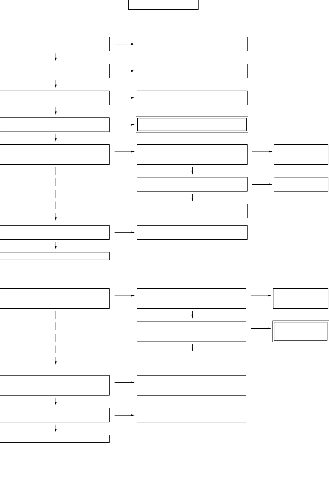
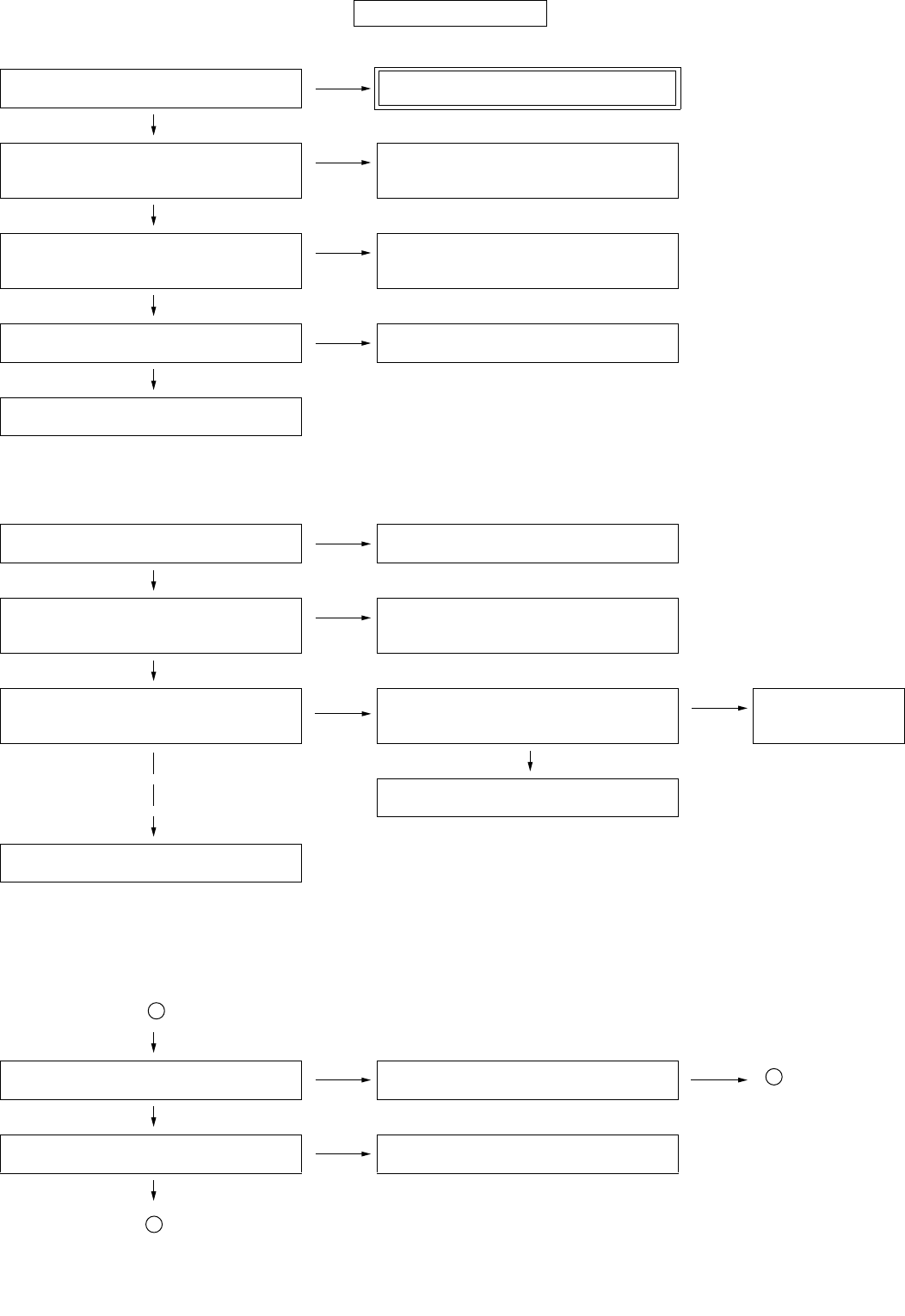
SERVICING CONCERNS
1. When requested, back up user’s handset data using SPST (SHARP Programme Support Tool). Otherwise, before servicing, warn the user that
data in the memory may be lost during repairs.
2. Upgrade the firmware to the latest version using SPST before returning the handset to the customer.
3. After repairs, inspect the handset (phone) according to the following flowchart.
4. When storing or transporting a PWB, put it into a conductive bag or wrap it in aluminum foil. (C-MOS IC may be damaged by electrostatic
charges.)
5. Do not leave fingerprints, etc. on ornamental parts including a cabinet, especially clear windows for main and sub displays. Wear fingerstalls to
avoid this.
Also, ensure not to leave fingerprints on the surface of main and sub display panels.
6. To prevent oxidation which causes connection problems, do not touch any terminals on the electric board, microphone, vibrator, earpiece and
speaker.
When handling these parts, wear fingerstalls. Should you touch these parts, clean them with a soft dry cloth.
Always wear fingerstalls when handling a shield case on the electric board. Otherwise oxidation may occur causing handset performance deterio-
ration.
7. The FPC is a precision device. Handle it carefully to prevent any damages.
8. Do not expose the moisture sensor to liquids.
If the sheet gets wet, red ink runs. In this case, replace the sheet with a new one.
Be careful about your perspiration.
9. Before you disassemble or reassemble handset, make sure to remove the Li-Ion battery.
10.Be sufficiently careful with static electricity of integrated circuits and other circuits. Wear static electricity prevention bands whilst servicing.
Repairs are completed.
(Fixed parts have been checked for proper operation.)
Check IMEI NO./Operator code (Destination)/
Firmware version by Identity function of SPST.
Inspect each device using performance check
adjustment function of SPST.
Carry out RF performance check with SPST.
All completed.
902SH
ii
CONFIDENTIAL
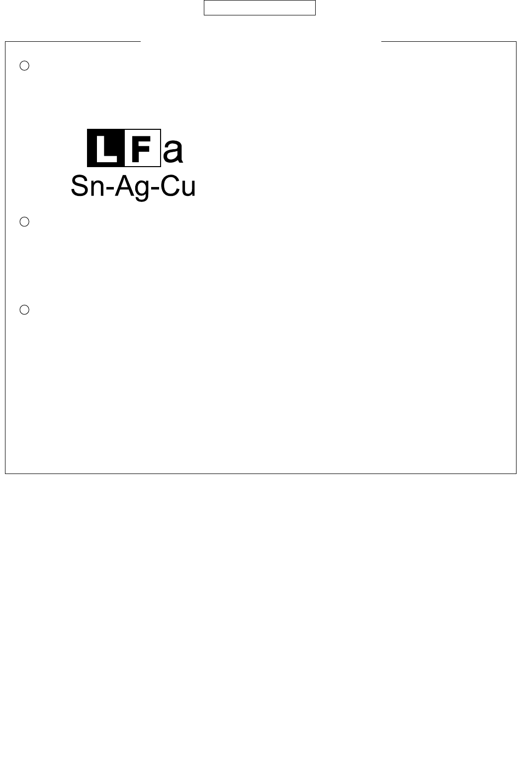
Employing lead-free solder
This model employs lead-free solder.
This is indicated by the “LF” symbol printed on the PWB and in the service manual.
The suffix letter indicates the alloy type of the solder.
Example:
Indicates lead-free solder of tin, silver and copper.
Using lead-free solder
When repairing a PWB with the “LF” symbol, only lead-free solder should be used. (Using normal tin/lead alloy solder may
result in cold soldered joints and damage to printed patterns.)
As the melting point of lead-free solder is approximately 40ºC higher than tin/lead alloy solder, it is recommended that a
dedicated bit is used, and that the iron temperature is adjusted accordingly.
Soldering
As the melting point of lead-free solder (Sn-Ag-Cu) is higher and has poorer wettability (flow), to prevent damage to the land
of the PWB, extreme care should be taken not to leave the bit in contact with the PWB for an extended period of time.
Remove the bit as soon as a good flow is achieved.
The high content of tin in lead free solder will cause premature corrosion of the bit.
To reduce wear on the bit, reduce the temperature or turn off the iron when it is not required.
Leaving different types of solder on the bit will cause contamination of the different alloys, which will alter their
characteristics, making good soldering more difficult.
It will be necessary to clean and replace bits more often when using lead-free solder. To reduce bit wear, care should be
taken to clean the bit thoroughly after each use.
PRECAUTIONS FOR USING LEAD-FREE SOLDER
1
2
3

902SH
1 – 1
CONFIDENTIAL
Phone902SHService ManualService ManualMarketE
CHAPTER 1. GENERAL DESCRIPTION
[1] Specifications
FOR A COMPLETE DESCRIPTION OF THE OPERATION OF THIS UNIT, PLEASE
REFER TO THE OPERATION MANUAL.
General: Quad - band (W-CDMA/GSM 900 MHz/
DCS 1800 MHz/PCS 1900MHz)
GPRS-enabled
WAP, MMS, SMS
Dimensions
(folded, exclud-
ing the aerial)
(W x H x D): 50 x 102 x 26 mm
Weight: 149 g
Battery operating
temperature: 0°C - 40°C
Main display: Display dimensions: 2.4 inch
Resolution: 240 x 320 pixels
LCD display: TFT 262,144 colours with backlight
LCD back light: LED back light white colour LEDs
Sub display: Resolution: 72 x 12 pixels
LCD display: STN B/W LCD with back light
Camera: CCD 2M pixels built-in camera
Zoom: Wide and zoom mode
[Supported 40 (when image size is
160 x 320 pixels) x zoom]
Lens: (Wide) F3.3, f = 4.85 mm
(Tele) F4.9, f = 9.7 mm
Sub Camera: CMOS 110K pixels built-in camera
Lens: F2.8, f = 1.7 mm
Sound: 64-polyphonic ring melodies
Stereo Speakers
Mobile light: 3 colours (RGB)
External DC
supply voltage: 5.2 V
Battery: 3.7 V, 870 mAh, Li-Ion
Standby time: Up to 240 hours (3G mode)
Up to 250 hours (GSM mode)
Talk time: Up to 150 minutes (3G mode))
Up to 240 minutes (GSM mode)
Others: Side key
Infrared port 1.2 L/P (maximum distance 20 cm)
Connector for AC charger and data cable
Battery running time depends on the battery and SIM card as well as
the network conditions and usage.
Specifications for this model are subject to change without prior
notice.
902SH
1 – 2
CONFIDENTIAL
Licensed by Inter Digital Technology Corporation under one or more of the
following United States Patents and/or their domestic or foreign
counterparts and other patents pending, including U.S. Patents:
4,675,863: 4,779,262: 4,785,450: 4,811,420: 5,228,056: 5,420,896:
5,799,010: 5,166,951: 5,179,571 & 5,345,467
Powered by Mascot Capsule /Micro3D Edition
Mascot Capsule is a registered trademark of HI Corporation
2002-2004 HI Corporation. All Rights Reserved.
Powered by JBlend Copyright 1997-2004 Aplix
Corporation. All rights reserved.
JBlend and all JBlend-based trademarks and logos
are trademarks or registered trademarks of Aplix
Corporation in Japan and other countries.
SD logo is a trademark.
Bluetooth is a trademark of the Bluetooth SIG, Inc.
T9 Text Input is licensed under one or more of the following: U.S. Pat. Nos.
5,818,437, 5,953,541, 5,187,480, 5,945,928, and 6,011,554;
Australian Pat. No. 727539; Canadian Pat. No. 1,331,057; United
Kingdom Pat. No. 2238414B; Hong Kong Standard Pat. No. HK0940329;
Republic of Singapore Pat. No. 51383; Euro. Pat. No. 0 842 463
(96927260.8) DE/DK, FI, FR, IT, NL,PT.ES,SE,GB; Republic of Korea Pat.
Nos. KR201211B1 and KR226206B1; and additional patents are pending
worldwide.
The Bluetooth word mark and logos are owned by the Bluetooth SIG, Inc.
and any use of such marks by Sharp is under license. Other trademarks
and trade names are those of their respective owners.
Contains Macromedia Flash technology by Macromedia, Inc.
Copyright 1995-2004 Macromedia, Inc. All rights reserved.
Macromedia, Flash, Macromedia Flash, and Macromedia Flash Lite are
trademarks or registered trademarks of Macromedia, Inc. in the United
States and other countries.
Licensed by QUALCOMM Incorporated under one or more of the following
United States Patents and/or their counterparts in other nations ;
4,901,307 5,490,165 5,056,109 5,504,773 5,101,501
5,506,865 5,109,390 5,511,073 5,228,054 5,535,239
5,267,261 5,544,196 5,267,262 5,568,483 5,337,338
5,600,754 5,414,796 5,657,420 5,416,797 5,659,569
5,710,784 5,778,338
This product is licensed under the MPEG-4 Visual Patent Portfolio License for the personal
and non-commercial use of a consumer to (i) encode video in compliance with the MPEG-4
Video Standard (“MPEG-4 Video”) and/or (ii) decode MPEG-4 Video that was encoded by a
consumer engaged in a personal and non-commercial activity and/or was obtained from a
licensed video provider. No license is granted or implied for any other use.
Additional information may be obtained from MPEG LA. See http://www.mpegla.com.
This product is licensed under the MPEG-4 Systems Patent Portfolio License for encoding
in compliance with the MPEG-4 Systems Standard, except that an additional license and
payment of royalties are necessary for encoding in connection with (i) data stored or
replicated in physical media which is paid for on a title by title basis and/or (ii) data which is
paid for on a title by title basis and is transmitted to an end user for permanent storage
and/or use. Such additional license may be obtained from MPEG LA, LLC. See
http://www.mpegla.com for additional details.
CP8 PATENT
TM
R
R
TM
C
TM
R
C
902SH
1 – 3
CONFIDENTIAL
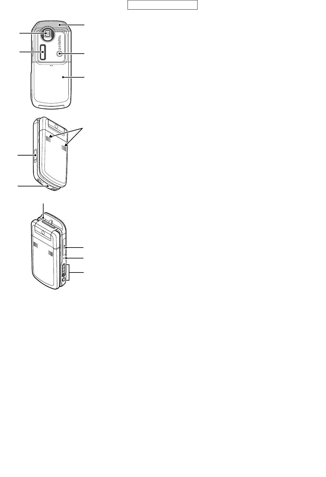
[2] Names of parts
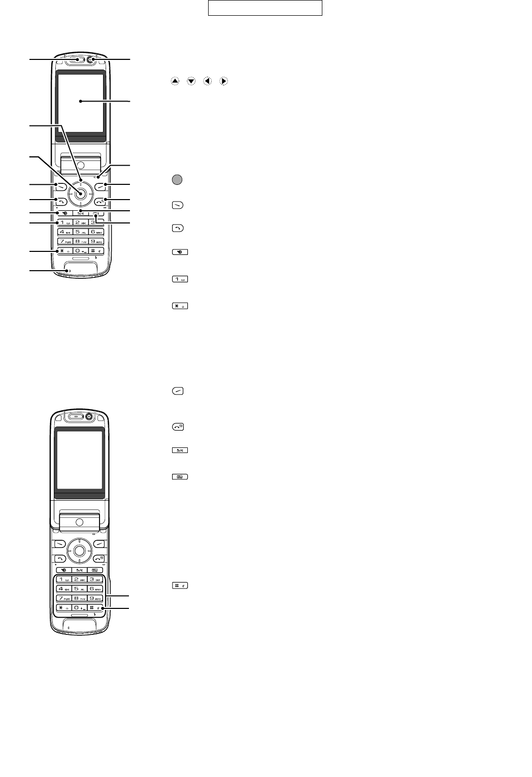
1. Earpiece
2. Navigation Keys (Arrow Keys):
Moves cursor to highlight a menu item, etc.
Up/Down arrow keys: Displays the Contacts List when pressed during stand-by.
Left arrow key:
Right arrow key:
Displays the message inbox when pressed during
stand-by.
Displays the monthly calendar when pressed during
stand-by.
3. Centre Key: Displays Main menu when pressed during stand-by,
then executes a function highlighted.
4. Left Soft Key: Executes a function at the bottom left of the screen.
Press during stand-by to display the Messaging screen.
5. Send/Redial Key: Makes or accepts calls, displays the All Calls screen in
stand-by mode.
6. Shortcut Key: Press to open the shortcut menu to access the desired
applications.
7. Voice Mail Key: Press and hold to connect to the Voice mail centre
automatically. (Depending on the SIM card.)
8. * /Shift Key: Switches character case between four modes: Abc, ABC,
123 and abc on the text entry screen.
Press to enter P, ?, – or * in stand-by mode.
1
2
3
4
5
6
7
8
9
11
10
12
13
14
15
16
9. Microphone
10. Sub Camera (Internal Camera)
11. Main Display
12. Microphone (for the viewer style of the display)
13. Right Soft Key: Executes the function at the bottom right of the screen.
Shortcut to “Vodafone live!” by opening the browser.
Press during stand-by.
14. End/Power Key: Ends a call and turns power on/off.
15. Clear/Back Key: Clears the characters before the cursor, returns to the
previous screen, etc.
16. Multimedia Key: Opens the Media Player screen.
17. Keypad:
1 key: Shortcut to the Voice mail centre. (Depending on the SIM
card.) Press and hold during stand-by.
2-9 keys: Press and hold during stand-by to display each speed dial
phone number.
0 key: Press and hold to enter +.
18. #/Flash Light Key: Switches symbol screens on the text entry screen.
Press and hold to switch languages on the text entry
screen.
Turns the flash/auxiliary light on or off in camera mode.
Press and hold during stand-by to switch Profiles settings
between the mode most recently activated and Silent
mode.
17
18
902SH
1 – 4
CONFIDENTIAL
19. Camera (External Camera)
20. Sub Display
21. Built-in Aerial: Warning: Do not cover the top of the phone with your hand
when in use as this may interfere with the performance of
the built-in aerial.
22. Mobile Light: Used as a flash or an auxiliary light in camera mode.
23. Battery Cover
24. VIDEO OUT/Handsfree Microphone Connector
25. External Connector: Used to connect either the charger or a USB data cable.
26. Stereo Speakers
19
20 22
23
21
24
25
26
27
28
29
30
27. Infrared Port: Sends and receives data via infrared.
28. Memory Card Slot Cover
29. Small Light: Used as a battery charge indicator.
30. Side Keys (Side-Up/Side-Down/Camera/Cancel):
Side-Up/Side-Down: (These two keys work in reverse with the viewer
position of the display.)
Moves the highlight up or down.
Press during stand-by or during a call to increase or
decrease the earpiece volume.
Press in camera mode to increase or decrease the
zooming ratio.
Camera Key: Displays the Main menu when pressed during stand-by,
then executes a highlighted function. Press and hold to
activate the camera.
Press and hold to display the Options menu.
Press during an incoming call to answer the call.
Press during a call to display the Call options.
Press halfway to lock the focus in camera mode.
Press (and hold) to take a picture with the camera.
Cancel Key: Press to return to the previous screen.
Press and hold to reject an incoming call.
Press during an incoming call to send a busy tone
to the caller.
Press to end the call.

902SH
1 – 5
CONFIDENTIAL
[3] List of Menu Functions
[4] Optional Accessories
Menu No./
Main Menu
1 Games & More
1 Games
2 Screensavers
3 Settings
4 Java Information
2 Vodafone live!
3 Media Player
4 Messages
1 Create New
2 Inbox
3 Drafts
4 Templates
5 Sent
6 Outbox
7 live! Studio
8 Messenger
9 Voice Mail
10 Cell Broadcasts
11 Area Info
12 Settings
13 Memory Status
5 Camera
6 My Items
1 Pictures
2 Videos
3 Sounds & Ringtones
4 Games & More
5 Bookmarks
6 My Saved Page
7 Text Templates
8 Other Documents
7 Organiser
1 Calendar
2 Alarms
3 Calculator
4 Voice Recorder
5 Scanner
6 Stopwatch
7 Tasks
8 World Clock
9 Countdown Timer
10 Expenses Memo
11 Phone Help
8 Contacts
1 Contacts List
2 Manage Group
3 Speeddial List
4 My Contact Details
5 Advanced
9 SIM Application
10 Connectivity
1 Bluetooth
2 Infrared
3 Network Settings
4 Internet Settings
5 Backup/Restore
11 Call Log
1 All Calls
2 Missed Calls
3 Received Calls
4 Dialled Numbers
5 Call Timers
6 Call Costs
12 Settings
1 Profiles
2 Display Settings
3 Sound Settings
4 Time&Date
5 Language
6 Call Settings
7 Video Call Settings
8 Security Settings
9 Memory Settings
10 Master Reset
Menu No./
Sub Menu1
Menu No./
Main Menu
Menu No./
Sub Menu1
TM
Lithium Ion Battery (XN-1BT90)
Cigarette Lighter Charger (XN-1CL30)
USB Data Cable (XN-1DC30)
AC Charger (XN-1QC30, XN-1QC31, XN-1QC32)
External Antenna Cable (XN-1AT90)
Audio Remote-Controller (XN-1AR90)
Car Holder (XN-1CH90)
Desktop Holder (XN-1DH90)
Stereo Headset (XN-1HS90)
Handsfree Microphone Unit (XN-1HU90)
Video Cable (XN-1VC90)
The above accessories may not be available in all regions.
For details, please contact your dealer.

902SH
2 – 1
CONFIDENTIAL
Phone902SHService ManualService ManualMarketE
CHAPTER 2. ADJUSTMENTS, PERFORMANCE CHECK, AND FIRMWARE
UPGRADE
SPST (SHARP Programme Support Tool) allows you to adjust settings, conduct performance checks, and upgrade the firmware.
[1] SHARP Programme Support Tool (SPST)
1. Installation/uninstallation
• Do not change the installation structures (see “2. Structure”).
• SPST cannot be installed on a PC if Windows Installer is not supported.
• The SPST installer does not include MFC that is required to run SPST. If not already installed, install MFC (DLLs including MFC42.DLL).
1.1. System requirements
The following are required for installation.
• OS: Windows 2000 Professional (SP3 or SP4) or Windows XP Home/Professional (SP1) *1
• PC: IBM/PC compatible *2
• HDD: 200 MB available space (or more)
• RAM: 256 MB or more (512 MB recommended)
• COM port: Windows compatible serial port
• Display resolution
XGA or higher
Basically use the default settings in Display Properties, however, small system font size is recommended. *3
(Display Properties → Settings → Advanced → General → Display → Font size)
• Recommended devices for serial connection between a PC and handsets (phones): *4, *5
The PC’s serial port
PCI serial expansion card
USB-UART serial conversion cable *6
Note
[Important] Restrictions for stable operation of Windows/PC (IBM/PC compatible)
When using multiple USB-UART conversion cables, do not connect more than 2 cables (IO-DATA) or 3 cables (NEC) to a USB-HUB/BUS, and do not
change the connection of cables.
Do not connect other USB devices to the PC.
Whilst the PC is in use, avoid connecting/disconnecting cables and USB devices for stable serial communication for Windows/driver.
* SPST may run in other environments, however, the system may become unstable.
1.2. Procedure
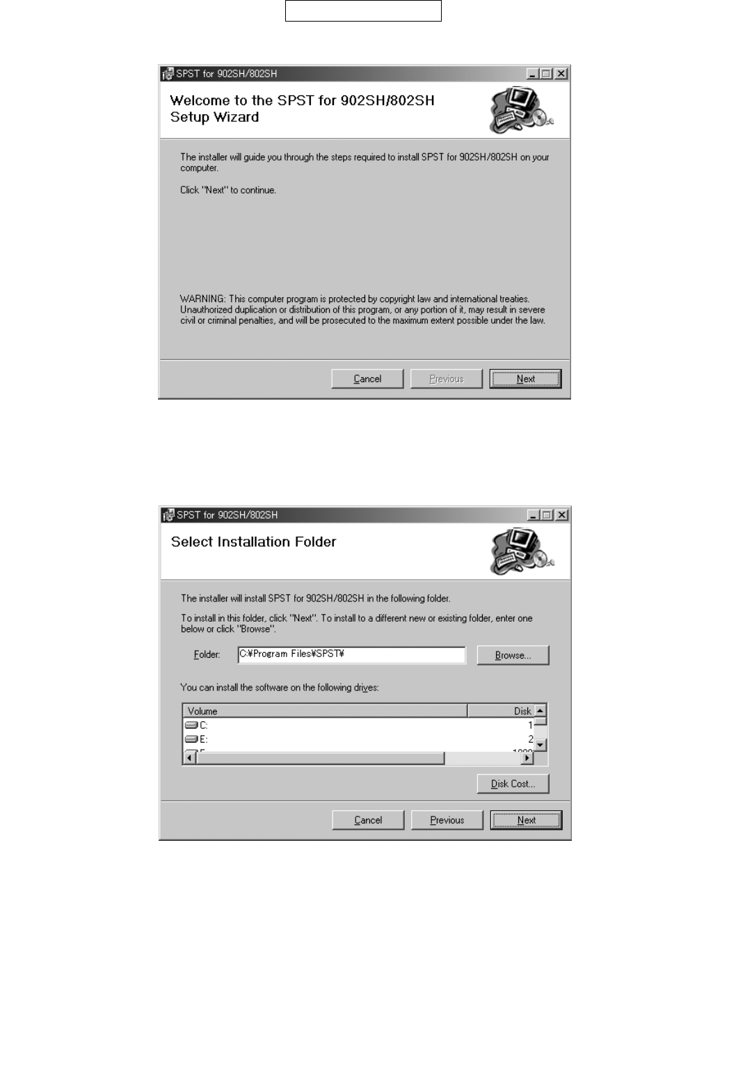
1.2.1 Installing SPST
Execute the “SPST.msi”.
Figure 1
[Caution]
When an older version of SPST has already been installed, uninstall it first as follows:
Through “Add/Remove Programs” in the Control Panel, remove the “SPST for 902SH/802SH”.
*1: SPST does not run on Windows 95, 98, 98 SE, and Me. The behaviour is not guaranteed on Windows XP Media Center Edition/Tablet Edition
and in the Virtual PC environment. Also, its compatibility with upcoming operating systems and service packs is not guaranteed.
*2: A brand name product is recommended. Minimum requirements: 1 GHz Pentium III processor and 256 MB of RAM, and compatibility with USB
2.0 specification for use of USB-UART serial conversion cables.
*3: Depending on the font size, the screen layout may change or some portions and characters may not be displayed on a XGA screen.
*4: Use only the specified PCI serial expansion card and USB-UART cables. Currently, no specific PCMCIA card is recommended.
*5: Transfer rate is 115 Kbps when using a PC’s standard serial port. When using a PCI/PCMCIA card or USB-UART conversion cable, its maxi-
mum transfer rate (115 Kbps, 230 Kbps or 460 Kbps) can be selected.
*6: Use cables of either manufacturer only.
902SH
2 – 2
CONFIDENTIAL
1) Setup screen
Figure 2
• Click “Next” to proceed.
• To cancel the installation, click “Cancel”.
2) Location selection screen
Figure 3
• Click “Next” to proceed.
• To cancel the installation, click “Cancel”.
[Caution]
Do not change the folder.
902SH
2 – 3
CONFIDENTIAL
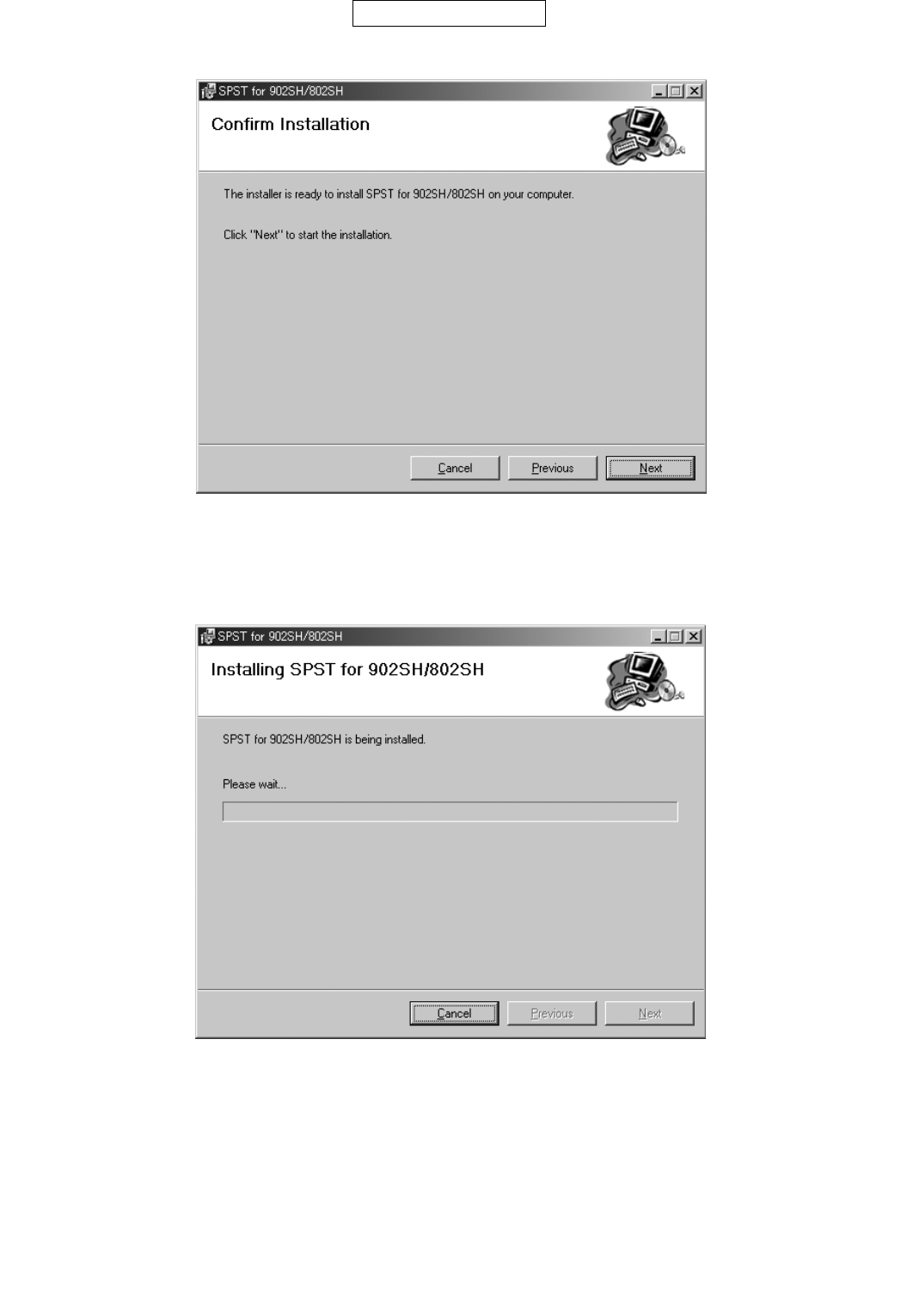
3) Confirmation screen
Figure 4
• Click “Next” to proceed.
• To cancel the installation, click “Cancel”.
4) Progress screen
Figure 5
• Wait until the installation is completed.
• To cancel the installation, click “Cancel”.
902SH
2 – 4
CONFIDENTIAL
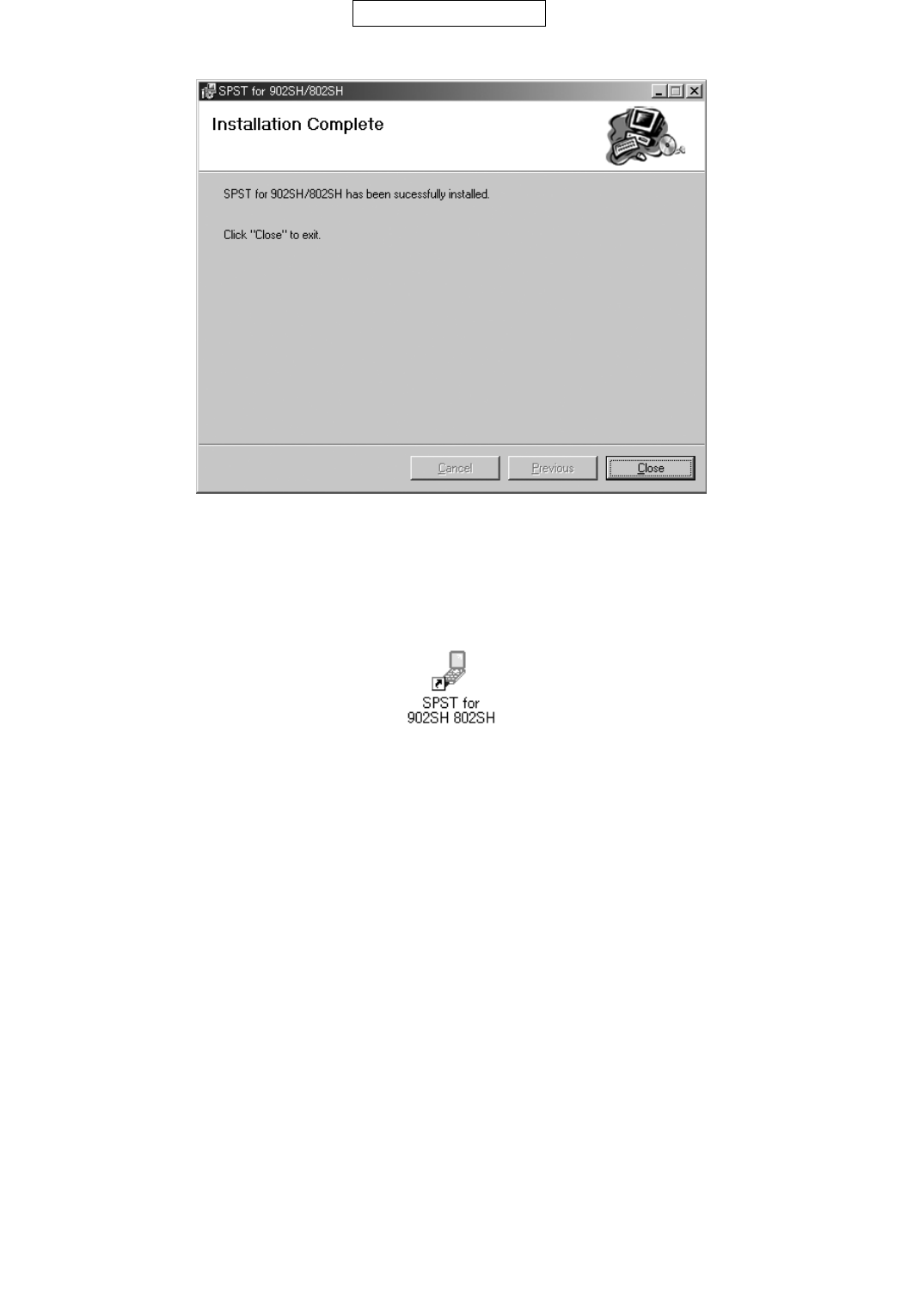
5) Complete screen
Figure 6
• The above screen appears when the installation has been successfully completed.
• Click “Close” to exit.
1.2.2 Starting SPST
• When the installation has been completed, the shortcut icon shown below is created on your desktop.
Figure 7
• Double-click the icon to start SPST.
2. Structure
• Tool structure
3. Start-up
Connect a dongle to the PC.
Double-click the icon “SPST for 902SH/802SH” to launch.
SPST Ver.1.0: Main application
SHDownLoader Ver.3.0: Handset (Phone) software and data update utility
SHDiag Ver.1.0: Handset (Phone) adjustment and inspection utility
SHInfoView Ver.1.0: Handset (Phone) information display utility
SHPwdReset Ver.1.0: Handset (Phone) password reset utility
902SH
2 – 5
CONFIDENTIAL
4. Function (screen example)
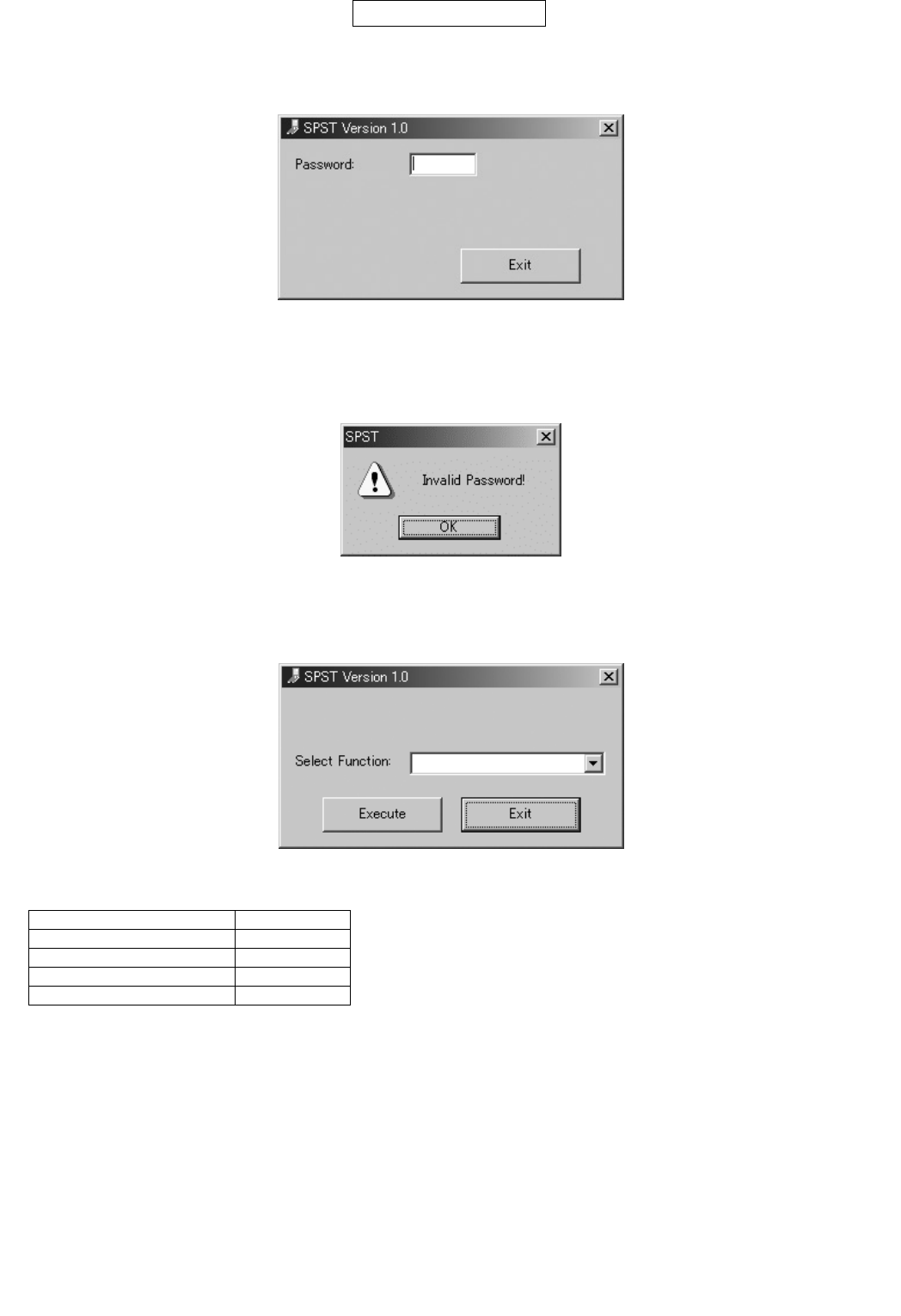
4.1. Password entry screen (after SPST start-up)
Figure 8
• Type in the specified password and press “Enter” on the keyboard.
• Click “Exit” on the screen to quit.
The screen below appears if the password is incorrect. Click “OK” and enter the password again.
Figure 9
4.2. Function selection (after entering SPST password)
• Function selection screen.
Figure 10
• Select one of the following functions from the combo box and click “Execute”.
• Click “Exit” to quit.
Selecting “SHDownLoader” See page 2-6
Selecting “SHDiag” See page 2-10
Selecting “SHInfoView” See page 2-13
Selecting “SHPwdReset” See page 2-15
Selecting “Change Password” See page 2-17
902SH
2 – 6
CONFIDENTIAL
4.3. Functions
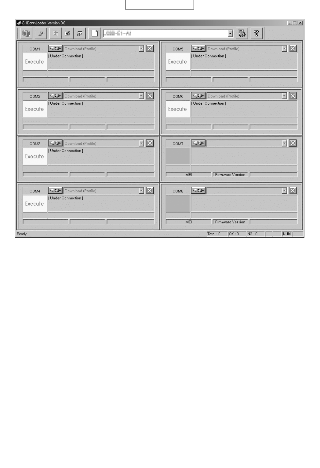
4.3.1 SHDownLoader
1) Basic functions
• SHDownLoader is the updating tool that is supported in Windows 2000/XP and designed for 902SH.
• SHDownLoader allows simultaneous updating operation via serial communication for up to 8 handsets (phones). *1
• A PC and handsets (phones) can be connected via serial connection by using the PC’s serial port, serial ports added by using PCI/PCMCIA cards
or USB-UART serial conversion cables.
• Batteries can be used to power handsets (phones), however, we recommend that you use chargers.
Note
2) Screen description
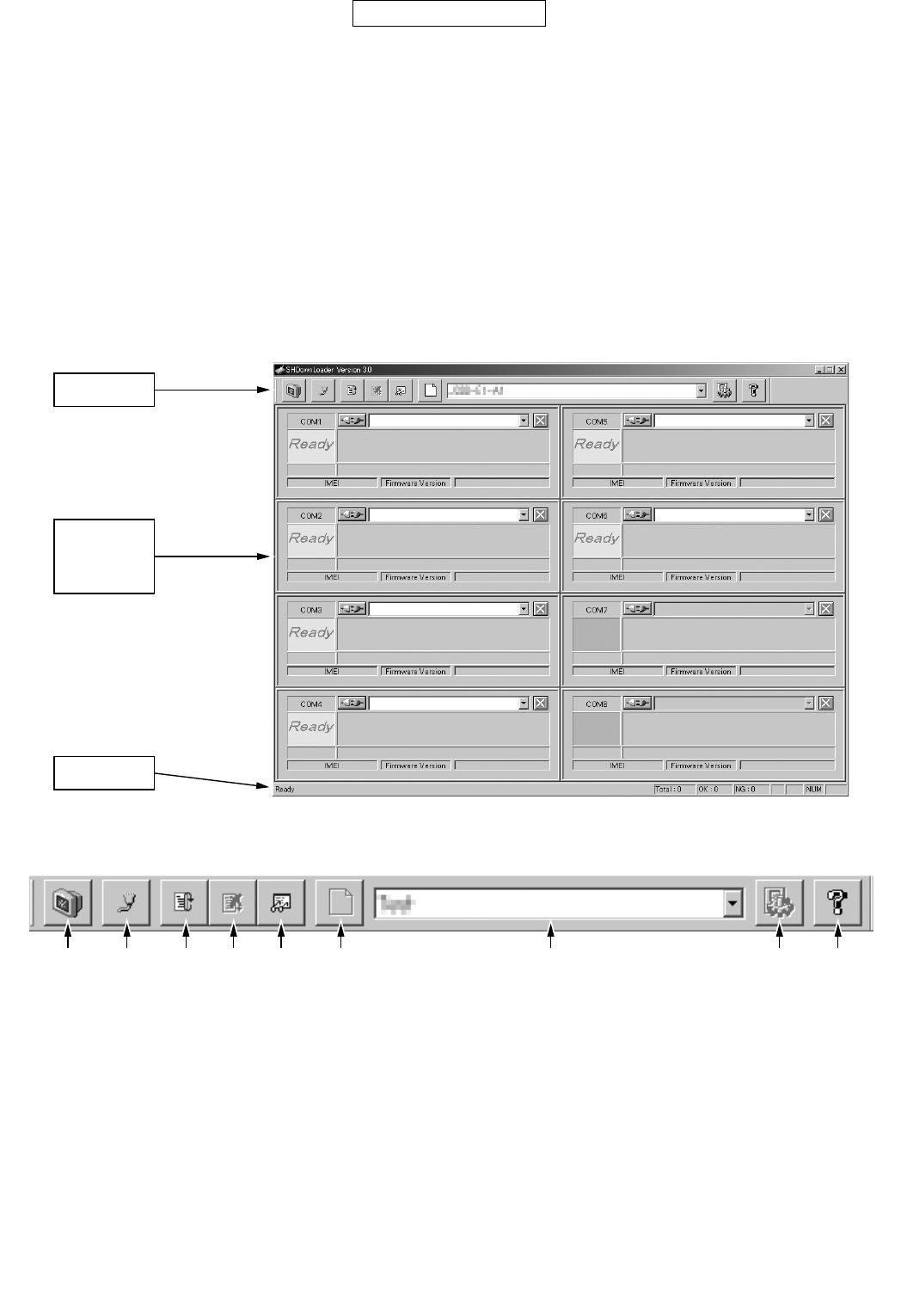
2) - 1. Main screen
Figure 11
2) - 2. Tool bar
Figure 12
*1: The maximum number of handsets (phones) may vary depending on the PC’s performance, devices used to add serial ports, etc. For details,
refer to the restrictions in “Important” below.
1. Exit Application: Close SHDownLoader.
2. Setup Option: Adjust optional settings.
3. Start All Ports: Start the operation for all the ports at once.
4. Stop All Ports: Stop the operation for all the ports at once.
5. View Actual Result: The operation result appears.
6. Create Profile: Create a new profile.
7. Select Profile: Select a profile.
8. Edit Profile: Edit a profile.
9. View Application Information: Show the version of SHDownLoader, etc.
Tool Bar
Status Bar
Port Field
[for up to
8 handsets
(phones)]
1 2 3 4 5 6 7 8 9
902SH
2 – 7
CONFIDENTIAL
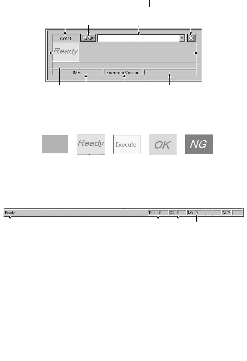
2) - 3. Port field
Figure 13
2) - 4. Status bar
Figure 14
1. Port Name: The (logical) port name appears.
2. Connect: Execute a selected function for the port only.
3. Select Function: Select a function for the port only.
4. Stop: Terminate an ongoing operation for the port only.
5. Status The operation status appears (see below).
6. Information: Show details of the operation, error, etc.
7. Rate/Progress: The progress bar appears with %.
8. IMEI: IMEI of the handset (phone) appears.
9. Firmware Version: Show information for handset (phone) identification.
10. Profile The last executed profile name appears whilst a profile is in progress. When the profile is completed, the dis-
play changes to its name.
1. Move the mouse cursor to “Tool Bar” items to see Tips (descriptions).
2. Show the total number of updated handsets (phones).
3. Show the total number of successfully updated handsets (phones).
4. Show the total number of handsets (phones) with update failure.
1
78 9 10
5 6
32 4
Unavailable Cancelled/failedCompletedIn progressReady
1 2 3 4
902SH
2 – 8
CONFIDENTIAL
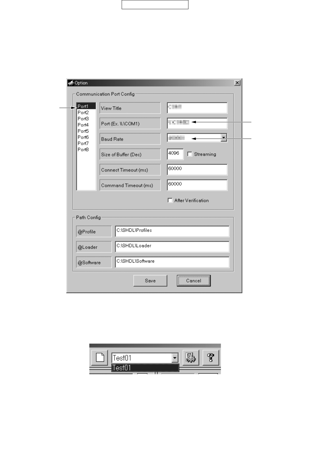
3) Option Settings
Adjust settings in Option when you use SHDownLoader for the first time or when the serial port connection is changed. Click “Setup Option” on “Tool
Bar” to open the screen and follow the procedures below.
1. Select a port from the list on the left.
2. In the field next to “Port (Ex. \\.\COM1)”, enter the corresponding serial port name.
3. Set a value for “Baud Rate” according to the serial port.
After performing these procedures for all the required ports, click “Save” to save the settings.
* Do not change settings in other fields.
Figure 15 Option Screen
When the settings are correct, “Ready” appears in the corresponding Port Field on Main Screen.
* When a USB-UART serial conversion cable is in use, assigned COM ports may vary as the system environment changes.
4) Procedures
Updating handsets (phones)
Figure 16
• From the “Select Profile” (combo box) on “Tool Bar”, select a profile.
• Click “Start All Ports” on “Tool Bar”. According to the selected profile, all handsets (phones) will be updated via the corresponding ports set up in
“Option”.
• When you select a function from “Select Function” in “Port Field” and click “Connect”, handsets (phones) will be updated according to the profile
specified for the port.
1
2
3
902SH
2 – 9
CONFIDENTIAL
Figure 17
• When you start updating, “Status/Information” in “Port Field” changes to “Execute/Under Connection” as shown above, and then handsets
(phones) become ready for connection or power-on. Connect chargers to the handsets (phones).
• To stop updating all at once, click “Stop All Ports” on “Tool Bar”.
• To stop updating individually, click “Stop” in “Port Field”.
Note
* Depending on the handset (phone) status, it may take up to 1 minute before updating stops after you click “Stop All Ports” / “Stop” button.
* To restart updating for ports disabled due to an error, etc., follow the procedure above (click “Start All Ports” on “Tool Bar” and click “Connect” in
“Profile Field”).
5) Basic rewriting procedure for handset (phone)
1. Preparation
<When you start SHDownLoader for the first time>
1) Add a serial port to a PC.
2) Start SHDownLoader and adjust settings of serial ports in “Option”.
2. Rewriting procedure
<Preparation>
1) Start a PC after connecting all the necessary cables and other devices.
* When using a USB-UART conversion cable, make sure not to change the connection port. Otherwise the corresponding COM port will also
change.
* Communication may be disrupted if you connect cables or devices after starting a PC.
2) Start SHDownLoader.
* Always select the latest profile.
902SH
2 – 10
CONFIDENTIAL
<Rewriting>
1) Remove batteries from all the handsets (phones).
2) Connect communication cables to all the handsets (phones).
3) Click “Start All ME” to start rewriting for all the handsets (phones).
4) Connect a charger to all the handsets (phones).
5) After the rewriting is completed, disconnect the chargers and communication cables from the handsets (phones).
<Initialisation>
After the rewriting operation, initialise each handset (phone).
1) Install a battery to the handset (phone).
2) Press the “End/Power” key for approx. 2 seconds.
3) The display indicates initialisation is in progress, and in approx. 8 minutes, indicates the completion.
4) Press the “End/Power” key until the display turns off.
5) Press the “End/Power” key for approx. 2 seconds.
6) Wait until the stand-by screen appears.
7) Press the “End/Power” key until the display turns off.
<After completing the operation>
• When this application is finished, the SPST function selection screen returns.
• Turn off the PC and disconnect the cables and other devices.
If you disconnect them before turning off the PC, Windows may not shot down.
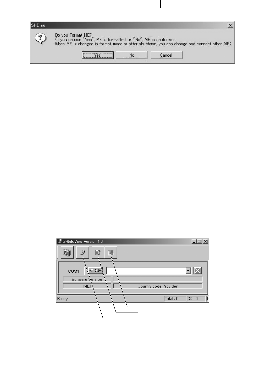
4.3.2 SHDiag
1) Overview
SHDiag allows you to perform various adjustments for handsets (phones) and to protect/unprotect the handset (phone) to be adjusted.
2) Operation screen
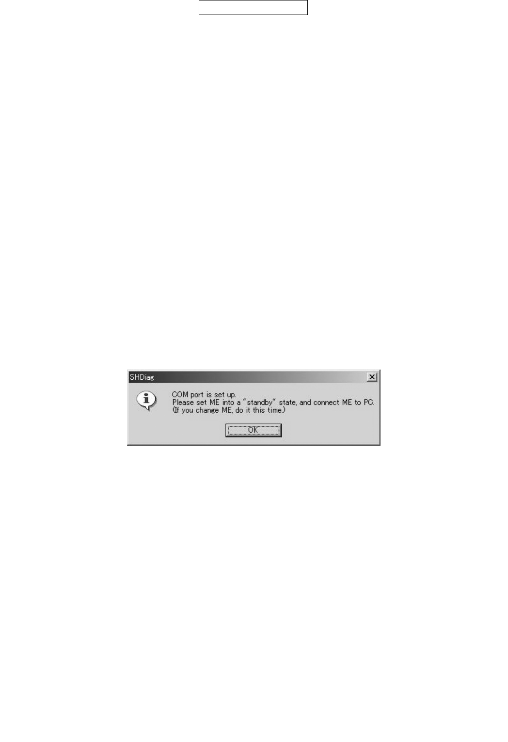
1. Connection confirmation window
Figure 18
At the start-up of SHDiag, the above window prompts you to connect a handset (phone) (ME). Connect a handset (phone) to be adjusted to a PC.
[User action]
1) Turn on a handset (phone) and set it to the stand-by mode. *1
2) Connect the handset (phone) to a PC.
3) Click “OK” on the window.
* When SHDiag is started unintentionally, click “OK” on the above window, and then click “Cancel” on the next COM port settings window.
[Caution]
Once a handset (phone) is connected, never disconnect/operate the handset (phone) or let the battery run out before exiting SHDiag.
*1: In the stand-by mode, one of the following screens appears.
•The main screen that appears after the start-up animation (Vodafone logo and Openwave logo), including the clock setting screen and the
network setup screen.
•The white background screen with “TEST PROGRAM” displayed.
902SH
2 – 11
CONFIDENTIAL
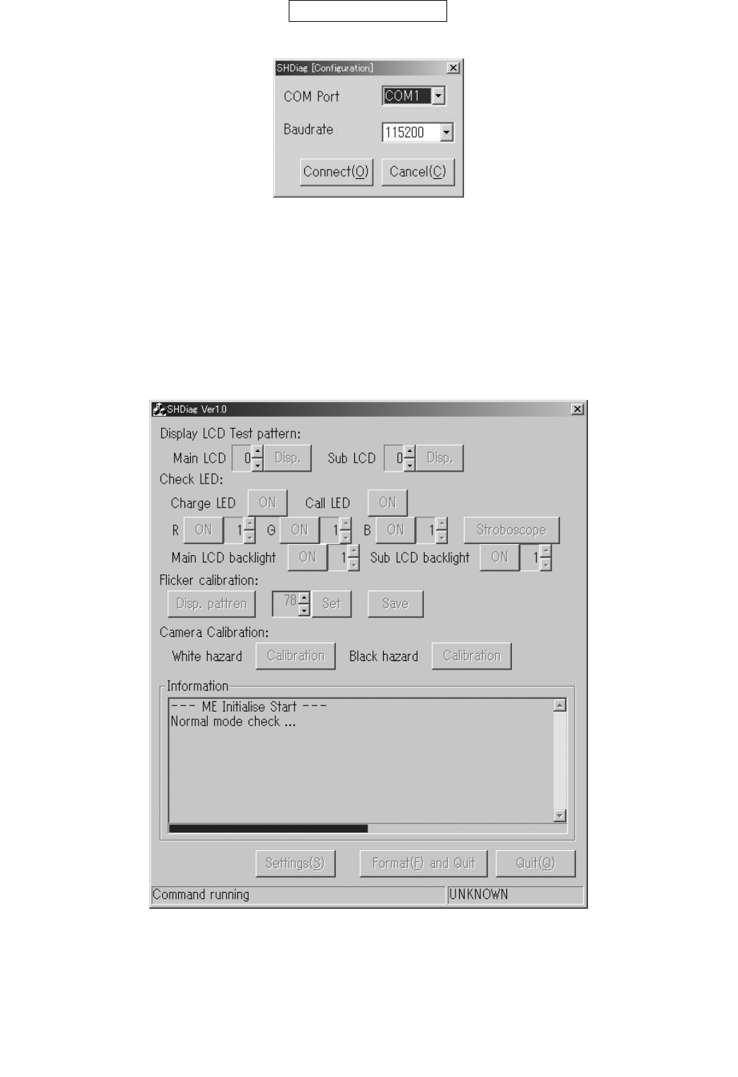
2. COM port settings window
Figure 19
After the connection confirmation window, the above window appears. From the list boxes, select a transfer rate (set to 115200 by default) and the
PC COM port that is connected to the handset (phone).
[User action]
1) Select the COM port connected to the handset (phone) from the “COM Port” list box.
2) Select a transfer rate for the PC to handset (phone) communication from the “Baudrate” list box (set to 115200 by default).
3) Click “Connect”.
* When SHDiag is started unintentionally, click “Cancel”.
3. Main window
Figure 20
After the COM port settings window, the main window above appears. The handset (phone) initial settings are performed, adjustment values are
obtained, and then adjustments are performed.
902SH
2 – 12
CONFIDENTIAL
[User action]
1) Wait until “--- ME Initialise Complete ---” is displayed.
2) Carry out adjustments.
• [Display LCD Test pattern]: Displays a test pattern on the handset (phone) display.
“Main LCD” is for the [main display] display, and “Sub LCD” for the [sub display] display.
Click the spin button (up or down arrow) to select a test pattern number. Click “Disp.” to display the test pattern on the handset (phone) dis-
play.
• [Check LED]: Turns on/off or controls brightness of the charge LED [red light on the side of the handset (phone)], call LED [green light on
the side of the handset (phone)], three-colour LED, and the display backlight.
To turn on/off the charge LED or call LED, click “ON” / “OFF” next to “Charge LED” or “Call LED” respectively.
For the three-colour LED, use “R”, “G”, or “B” to control each colour. To turn on/off the LED, click “ON” / “OFF”. To change the brightness,
click the spin button (up or down arrow). To check the strobe light, click “Stroboscope” with the three-colour LED illuminated.
As for the display backlight, “Main LCD backlight” is for the main display, and “Sub LCD backlight” for the sub display. To turn on/off the
backlight, click “ON” / “OFF”. To change the brightness, click the spin button (up or down arrow).
• [Flicker Calibration]: Adjusts the flicker of the main display.
Click “Disp. Pattern” to display the flicker calibration screen.
Click the spin button to change the flicker calibration value.
Click “Set” to temporarily use the value for the handset (phone).
Click “Save” to apply the value.
• [Camera Calibration]: Automatically corrects bright and dark defects.
To perform the bright defect correction, click “Calibration” next to “White hazard”.
To perform the dark defect correction, click “Calibration” next to “Black hazard”.
3) To initialise the handset (phone) and exit SHDiag after completing adjustments, click “Format and Quit”.
• To change handsets (phones), click “Settings”. After the necessary operation on the handset (phone) change confirmation window, the con-
nection confirmation window appears. Change handsets (phones) here.
• To exit SHDiag without handset (phone) initialisation, click “Quit”.
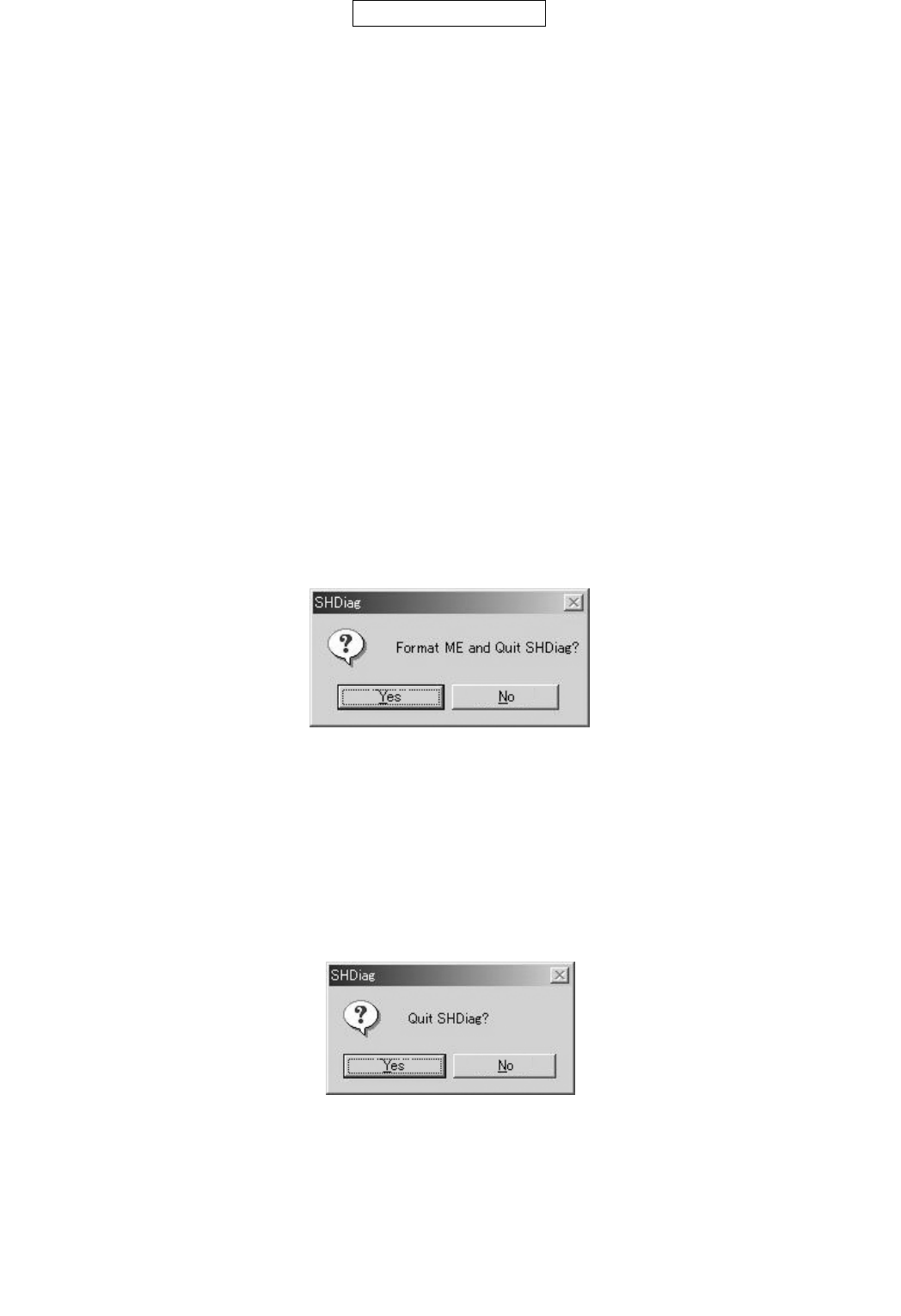
4. Quit confirmation window 1
Figure 21
The above window appears when “Format and Quit” is clicked on the main window. Handset (Phone) initialisation starts and SHDiag closes.
[User action]
1) To initialise the handset (phone) and exit SHDiag, click “Yes”.
• Click “No” not to exit SHDiag.
• When “Yes” is clicked, initialisation starts and SHDiag closes. Now, disconnect the handset (phone) and the PC.
5. Quit confirmation window 2
Figure 22
The above window appears when “Quit” is clicked on the main window. The handset (phone) turns off and SHDiag closes.
[User action]
1) To turn off the handset (phone) and exit SHDiag, click “Yes”.
• Click “No” not to exit SHDiag.
• When “Yes” is clicked, the handset (phone) turns off and SHDiag closes. Now, disconnect the handset (phone) and the PC.
902SH
2 – 13
CONFIDENTIAL
6. Handset (Phone) change confirmation window
Figure 23
The above window appears when “Settings” is clicked on the main window. Before changing handsets (phones), specify whether to initialise the
handset (phone) or not. After initialisation or handset (phone) change, make communication settings again.
[User action]
1) Click “Yes” to initialise the handset (phone) and make communication settings again.
• Click “No” to turn off the handset (phone) and make communication settings again.
• Click “Cancel” not to make communication settings.
• When “Yes” is clicked, initialisation starts and the connection confirmation window appears. Now, disconnect the handset (phone) and the
PC, and connect another handset (phone).
• When “No” is clicked, the handset (phone) turns off and the connection confirmation window appears. Now, disconnect the handset (phone)
and the PC, and connect another handset (phone).
• When this application is finished, the SPST function selection screen returns.
4.3.3 SHInfoView
1) Function
Handset (Phone) information appears on the screen.
• Displayed information:
IMEI
Software version
Country code
Provider name
* For a screen example, refer to “Appendix 1: Handset (Phone) information”.
• Batteries can be used to power handsets (phones), however, we recommend that you use chargers.
2) Operation
Figure 24
* The initial setting file and the option file are created during the start-up process if they do not exist.
Stop
Start
Option
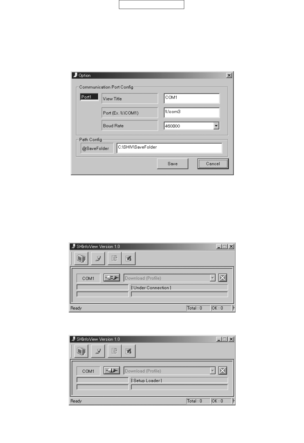
902SH
2 – 14
CONFIDENTIAL
1. Change the option settings if necessary.
Default settings, when the tool is started for the first time, are as follows:
Port1
View Title COM1
Port
Baud Rate 115200bps
Make sure to set the “Port” at the first start after the installation.
Example: COM3 port at 460,800 bps
Figure 25
* Set following to restore the PC settings.
Port \\.\COM1
Baud Rate 115200
After completing changes, click “Save”.
2. Connect the communication cable to the handset (phone).
* 10-pin flat cable which connects the PC’s serial port and the handset’s (phone’s) handsfree microphone connector.
3. Click “Start”.
Figure 26 Waiting for connection
4. Supply power to the handset (phone).
Figure 27 Loading information
Refer to Appendix 1 for the display after loading information.
5. When this application is finished, the SPST function selection screen returns.

902SH
2 – 15
CONFIDENTIAL
Appendix 1: Handset (Phone) information
Figure 28 Screen example
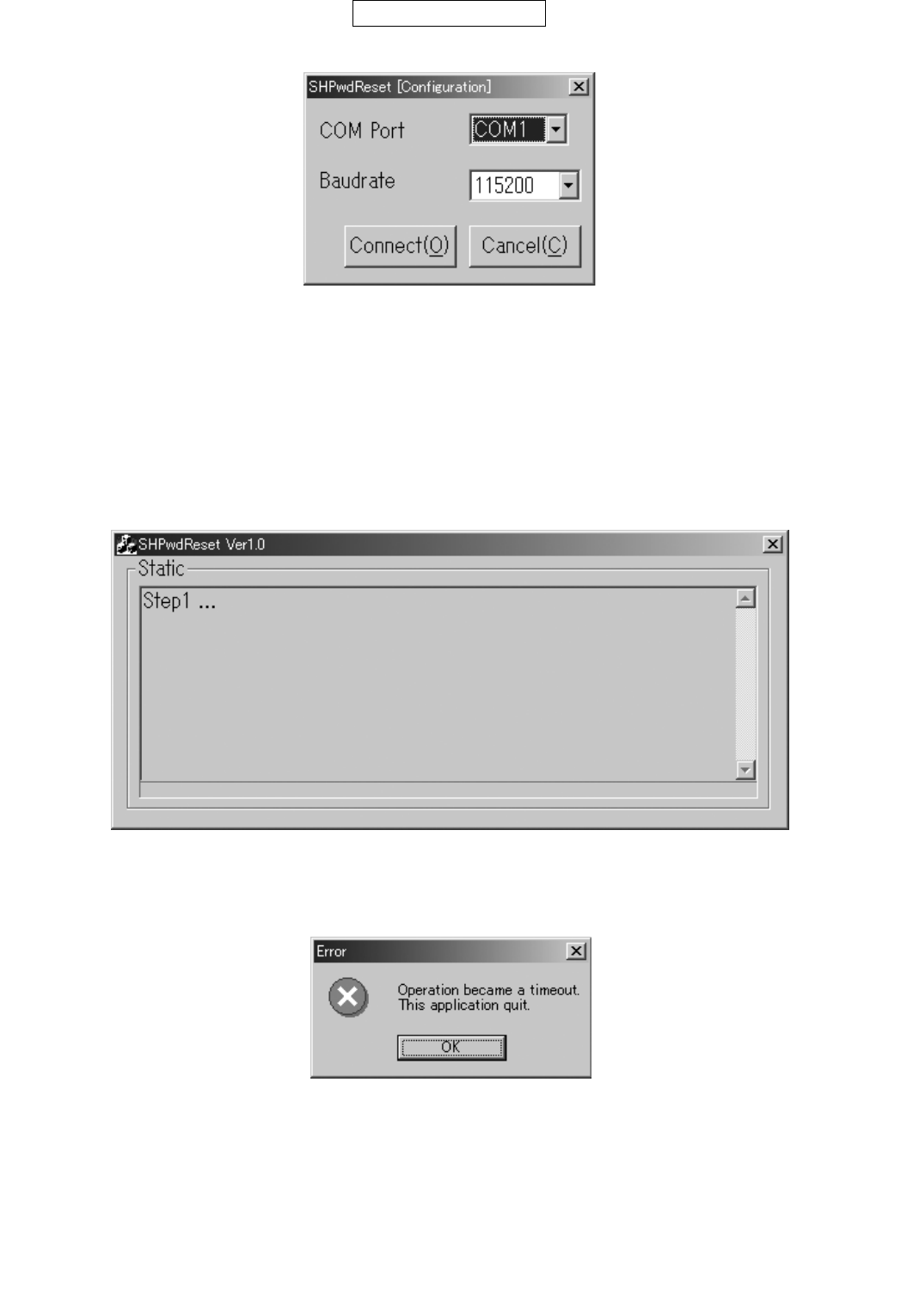
4.3.4 SHPwdReset
1) Overview
SHPwdReset allows you to reset all the handset (phone) passwords to the factory defaults.
2) Operation Screen
1. Connection Confirmation Window
Figure 29
At the start-up of SHPwdReset, the above window prompts you to connect a handset (phone) (ME). Connect a handset (phone) to be adjusted to
a PC.
[User Action]
1) Turn on a handset (phone) and set it to the stand-by mode. *1
2) Connect the handset (phone) to a PC.
3) Click “OK” on the window.
* When SHPwdReset is started unintentionally, click “OK” on the above window, and then click “Cancel” on the next COM port settings window.
[Caution]
Once a handset (phone) is connected, never disconnect/operate the handset (phone) or let the battery run out before exiting
SHPwdReset.
*1: In the stand-by mode, one of the following screens appears.
•The main screen that appears after the start-up animation (Vodafone logo and Openwave logo), including the clock setting screen and the
network setup screen.
•The white background screen with “TEST PROGRAM” displayed.
Countr
y
code: Provider nameSoftware VersionIMEI
902SH
2 – 16
CONFIDENTIAL
2. COM port settings window
Figure 30
After the connection confirmation window, the above window appears. From the list boxes, select a transfer rate (set to 115200 by default) and the
PC COM port that is connected to the handset (phone).
[User Action]
1) Select the COM port connected to the handset (phone) from the “COM Port” list box.
2) Select a transfer rate for the PC to handset (phone) communication from the “Baudrate” list box (set to 115200 by default).
3) Click “Connect”.
* When SHPwdReset is started unintentionally, click “Cancel”.
3. Main Window
Figure 31
When the COM port settings window closes, SHPwdReset starts to reset the handset (phone) passwords immediately.
If the connection fails, the error message below appears.
Figure 32
On the above window or when the operation is successfully completed, click “OK” to exit SHPwdReset and return to the SPST function selection
screen.

902SH
2 – 17
CONFIDENTIAL
4.3.5 Change Password
Figure 33 Password change screen
• Enter a new password, enter it again for confirmation, and click “Setting”.
• Click “Cancel” to quit.
• After completing or cancelling the operation, the SPST function selection screen returns.
* For allowable symbols and alphanumeric characters, see “Password entry screen (after SPST start-up)”.

902SH
2 – 18
CONFIDENTIAL
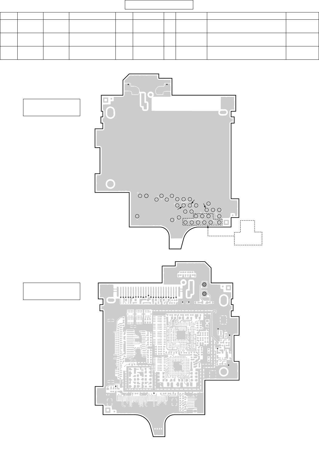
[2] Test points
Main PWB
No. Checker Ref. Name φOutput Input Function Remarks
1 TP1002 BANDSEL_1 0.3 IC1000 →Band switching Back-up
2 O TP1003 VRTC15 1.2 IC1204 →IC1000 RTC 1.5 V power supply
3 TP1004 PCMDATA–B 0.3 IC1001,
IC1200
→IC1000 PCM data
4 TP1005 PCMDATA–A 0.3 IC1000 →IC1001,
IC1200
PCM data
5 O TP1006 RTCCLK 1.2 IC1000 →IC1001,
IC1200,
IC1400
32.768 kHz output
6 O TP1007 SYSCLK2 1.2 IC1000 →13MHz
7 TP1008 M_LCD_I2CCLK 0.3 IC1000 →IC3000 I2C clock
8 TP1009 SYSCLK0 1.2 IC1000 →IC1001 13MHz Back-up
9 TP1010 M_LCD_I2CDAT 0.3 IC1000 ↔IC3000 I2C data
10 TP1011 PCMCLK 0.3 IC1000 →IC1001,
IC1200
PCM clock
11 TP1012 PCMSYN 0.3 IC1000 →IC1001,
IC1200
PCM sync
12 O TP1013 TP-IN 1.2 →IC1000 Mandatory test mode
13 O TP1014 SYSCLK1 1.2 IC1000 →IC1500,
IC1502,
IC1600
13MHz
14 TP1015 UARTRX3 0.3 IC1001 →IC1000 Bluetooth UART Rx
15 TP1016 UARTTX3 0.3 IC1000 →IC1001 Bluetooth UART Tx
16 TP1017 UARTCTS3 0.3 IC1001 →IC1000 Bluetooth UART CTS
17 TP1018 UARTRTS3 0.3 IC1000 →IC1001 Bluetooth UART RTS
18 TP1019 KeyCK1 1.2 CN1000 →Key FPC
unit
Check for the key unit insertion
19 TP1020 KeyCK2 1.2 CN1000 →Key FPC
unit
Check for the key unit insertion
20 O TP1021 VBT29 1.2 IC1002 →IC1001 Bluetooth IC power supply (2.9 V)
21 TP1022 RRESOUT2 0.3 IC1000 →IC1001 Bluetooth IC reset
22 TP1023 CLKREQ 0.3 IC1000 →IC1001,
IC1200,
IC1400
CLK request signal
23 TP1024 WP_N 1.2 IC1000 →IC1100 VPP Back-up
24 O TP1200 VBATT 1.2 CN1200 →Handset (Phone) power supply
(battery terminal)
25 O TP1201 VBATT 1.5 CN1200 →Handset (Phone) power supply
(battery terminal)
26 O TP1202 VBATT 1.5 CN1200 →Handset (Phone) power supply
(battery terminal)
27 O TP1203 PRGDET 1.2 JK1600 →Q1204,
Q1205
Action trigger (Insert the socket to
turn on the power.)
ONSWB_N
28 TP1204 VCHG 1.2 Q1212 →Q1206 External supply power (at normal
voltage)
29 TP1205 CHPEG 1.2 IC1200 →Q1200 FET gate signal
30 O TP1206 SERVICE_N 1.2 Q1205 →IC1000 Rewrite mode and log mode
31 TP1207 BDATA 1.2 CN1200 →IC1200 Battery sense terminal
32 O TP1209 GND 1.2 GND →Earth
33 O TP1210 GND 1.5 GND →Earth
34 O TP1211 VBATIB 1.2 CN1200,
IC1202
→Handset (Phone) power supply
(BB)
35 O TP1212 GND 1.5 GND →Earth
36 O TP1213 ONSWB_N 0.5 Q1204,
Q1215
→IC1200 Action trigger (Insert the socket to
turn on the power.)
37 O TP1215 BEARP 1.2 IC1200 →TP3055 Earpiece
38 O TP1216 BEARN 1.2 IC1200 →TP3054 Earpiece
39 O TP1217 PWRRST_N 1.2 IC1200 →IC1000 Power reset signal
40 O TP1218 SIMVCC 1.2 IC1200 →CN1201 Power supply for USIM

902SH
2 – 19
CONFIDENTIAL
41 O TP1219 SIMVCC 1.2 IC1200 →CN1201 Power supply for USIM
42 O TP1220 SIM I/O 1.2 IC1200 ↔CN1201 USIM data
43 O TP1221 SIM CLK 1.2 IC1200 →CN1201 USIM clock
44 O TP1222 SIM RESET 1.2 IC1200 →CN1201 USIM reset
45 O TP1223 VSRAM18 1.2 IC1206 →IC1101 SRAM power supply (1.8 V)
46 O TP1225 GND 1.2 GND →Earth
47 O TP1226 VCCR 1.2 IC1206 →CN3003 Back-up power supply
48 O TP1227 VANA15 1.2 IC1205 →Analogue power supply (1.5 V)
49 O TP1228 ONSWA_N 1.2 Key FPC
unit
→IC1200 Action trigger (Switch the key to
turn on the power.)
50 O TP1229 LEDR 1.2 LED1200 →IC1200 Charge LED
51 O TP1230 LEDG 1.2 LED1200 →IC1200 Incoming notifications LED
52 O TP1231 VMEM18 1.2 IC1200 →IC1100,
IC1101
Power supply for memory (1.8 V)
53 O TP1232 VDIG275 1.2 IC1200 →Digital power supply (2.75 V)
54 O TP1233 VDDB 1.2 IC1200 →RF power supply (2.75 V)
55 O TP1234 VDDA 1.2 IC1200 →RF power supply (2.75 V)
56 O TP1235 VCORE15 1.2 IC1200 →Core power supply (1.5 V)
57 O TP1236 LED1 1.2 LED1200 →IC1200 Charge LED
58 O TP1237 LED2 1.2 LED1200 →IC1200 Incoming notifications LED
59 O TP1301 VDCIO 1.2 CN1300 →Q1212 External supply power
60 TP1302 CTS (Rx voice) 1.2 CN1300 →IC1300 CTS (hands free Rx voice)
61 O TP1303 Manufacture
Specific
1.5 CN1300 →Q1301 UART detection signal
62 TP1304 RTS (Tx voice) 1.2 IC1300 →CN1300 RTS (hands free Tx voice)
Synchronisation Clock
63 O TP1305 TXD
USB D–
1.2 IC1300 →CN1300 UART1 Tx
USB D– line
64 O TP1306 RXD
USB D+
1.2 CN1300 →IC1300 UART1 Rx
USB D+ line
65 O TP1307 VBUS 1.2 CN1300 →IC1303 External USB VBUS
66 O TP1308 VUSB33 1.2 IC1303 →IC1300,
IC1000
USB power supply (3.3 V), USB
detection signal
67 TP1400 TSFRM 0.3 IC1500 →TS I/F frame sync signal GPIO Back-up
68 O TP1500 VDCDC 1.2 IC1504 →IC1504 DCDC power supply (1.5 to 2.5 V)
69 O TP1501 VTRAM25 1.2 IC1504 →IC1500 T4G RAM power supply (2.5 V)
70 O TP1502 VTRAM15 1.2 IC1504 →IC1500 T4G RAM power supply (1.5 V)
71 O TP1503 VDIG29 1.2 IC1504 →Digital power supply (2.9 V)
72 O TP1504 VTLVDS25 1.2 IC1504 →IC1500 T4G LVDS power supply (2.5 V)
73 O TP1505 VTLVDS15 1.2 IC1504 →IC1500 T4G LVDS power supply (1.5 V)
74 O TP1506 T4G NC1 1.2 IC1500 →IC1500 Check for peeling of T4G
75 O TP1507 T4G NC2 1.2 IC1500 →IC1500 Check for peeling of T4G
76 TP1600 A0 0.3 →Adress 0 Back-up
77 O TP1601 MIC2+ 1.2 MIC200 →IC1200 Mic bias2
78 O TP1602 MIC- 1.2 MIC201 →Mic earth
79 O TP1603 MIC1+ 1.2 Key FPC
unit
→IC1200 Mic bias1
80 O TP1604 JMIC 1.2 JK1600 →IC1200 Connector microphone
81 O TP1605 JEARR 1.2 IC1600 →JK1600 Connector EAR R-ch
82 O TP1606 JEARL 1.2 IC1600 →JK1600 Connector EAR L-ch
83 O TP1607 VAMP 1.2 IC1701 →JK1600 TV signal output
84 O TP1608 SP-L1 1.2 IC1603 →CN3003 Speaker 1 L-ch
85 TP1609 VVIB 1.2 IC1601 →VIB1600 Vibrator power supply
86 O TP1610 SP-R1 1.2 IC1603 →CN3003 Speaker 1 R-ch
87 O TP1611 SP-L2 1.2 IC1603 →CN3003 Speaker 2 L-ch
88 O TP1612 SP-R2 1.2 IC1603 →CN3003 Speaker 2 R-ch
89 O TP1613 UART0TX 1.2 IC1000 →JK1600 UART Tx software rewrite and log
90 O TP1614 UART0RX 1.2 JK1600 →IC1000 UART Rx software rewrite and log
91 O TP1800 BECLK 1.2 IC1500 →IC1800 27MHz clock output
No. Checker Ref. Name φOutput Input Function Remarks
902SH
2 – 20
CONFIDENTIAL
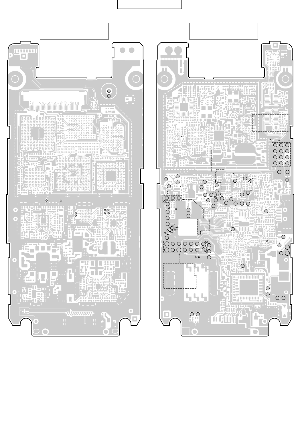
Figure 34 TEST POINT
MIC200
MIC201
SP031 SP032
SP012
SP014 SP001
SP002SP003
SP004
TP1013
TP1015
TP1016
TP1017
TP1018
TP1204
TP1205
TP1207
TP1603
TP1019 TP1020
TP1301
TP1200
TP1201
TP1202
TP1203
TP1506
TP1213
TP1614
TP1503
TP1601TP1608TP1234
TP1400
TP1215
TP1216
TP1602
TP1604 TP1605
TP1606
TP1607
TP1800 TP1611
VIB1600
VIB1601
TP1609
TP1600
TP1211
TP1507
TP1023
TP1236
TP1237 TP1504
TP1024
TP1004
TP1007
TP1012
TP1014
TP1002
TP1008
TP1010
TP1610
TP1612
TP1230
TP1232
TP1233
TP1235
SP019
SP020
SP028
TP1003
TP1229
SP027
TP1227
TP1501
TP1226
TP1502
TP1505
TP1009
TP1206
TP1225
TP1613
TP1308
TP1005 TP1011
TP1223
TP1217
TP1500
TP1006
TP1022
TP1209
SP009
SP015
SP016
SP017
SP018
TP1210
TP1228
TP1303
TP1212
TP1219
TP1220
TP1221
TP1222
TP1231
SP029
TP1302
TP1304
TP1021
TP1218
SP021
SP023
TP1305
TP1306
TP1307
SP008
SP022
MAIN PWB-A
(FRONT SIDE)
MAIN PWB-A
(REAR SIDE)

902SH
2 – 21
CONFIDENTIAL
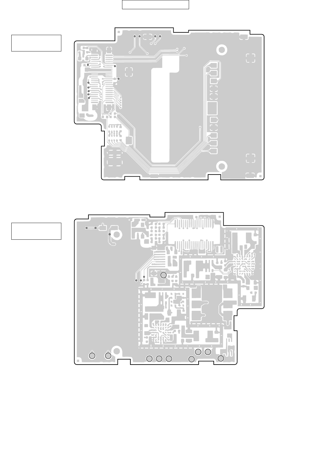
Display PWB
No. Checker Ref. Name φOutput Input Function Remarks
1 TP3002 VDON 1.2 IC1500 →IC3000 VD-LINK ON/OFF setting
2 TP3003 LCDCLK 1.2 IC1500 →IC3000 Display clock (6.5 MHz)
3 TP3004 VBATIB 1.2 CN1200,
IC1202
→Handset (Phone) power supply
(BB)
4 TP3005 GND 1.2 GND →Earth
5 TP3007 GND 0.3 GND →Earth
6 TP3008 BLED+ 1.2 IC2005 →TP3008 Main display/Sub display backlight
+, white LED boost output
7 TP3009 BLED – 1.2 TP3009 →IC2005 Main display backlight –, white
LED feedback circuit
8 TP3010 DUMMY1 0.3 IC3000 →IC3000 Check for peeling of LCDC
9 TP3011 DUMMY2 0.3 IC3000 →IC3000 Check for peeling of LCDC
10 TP3012 LVSYN 1.2 IC3000 →IC1500 VSYNC output signal
11 TP3018 VDD2 0.3 Main
display
→DC/DC convertor output
12 TP3019 VCCR 1.2 IC1206 →CN3003 Back-up power supply
13 TP3024 FLIP_R 0.3 CN3003 →IC1000 Rotation detection
14 TP3025 BLED+ 1.2 IC2005 →TP3008 Main display/Sub display backlight
+, white LED boost output
15 O TP3026 VUDIG29 0.3 IC3001 →Digital power supply (2.9 V)
16 O TP3027 VUDIG18 0.3 IC3002 →Digital power supply (1.8 V)
17 O TP3028 VUDIG25 0.3 IC3004 →Digital power supply (2.5 V)
18 TP3031 VDWAIT 1.2 IC3000 →IC1500 WAIT signal
19 TP3032 M_LCD_I2CDATA 1.2 IC1000 ↔IC3000 I2C data
20 TP3033 M_LCD_I2CDCLK 1.2 IC1000 →IC3000 I2C clock
21 TP3034 PDW_ECO 1.2 IC1000 →IC3001,
IC3002,
IC3004
REG ECO mode signal
22 TP3035 PDW_CE 1.2 IC1200 →IC3001,
IC3002,
IC3004
REG enable signal
23 TP3036 LCDRST 1.2 IC1500 →IC3000 Display RST signal
24 TP3037 LCDINT 1.2 IC3000 →IC1500 Display INT signal
25 TP3048 TXDTP 1.2 IC1500 →IC3000 VD-LINK operational data input
26 TP3049 TXDTN 1.2 IC1500 →IC3000 VD-LINK operational data input
27 TP3050 TXCKP 1.2 IC1500 →IC3000 VD-LINK operating clock input
28 TP3051 TXCKN 1.2 IC1500 →IC3000 VD-LINK operating clock input
29 O TP3053 BLED – 1.2 TP3009 →IC2005 Display backlight –, white LED
feedback circuit
30 TP3054 BEARN 0.3 IC1200 →TP3054 Earpiece
31 TP3055 BEARP 0.3 IC1200 →TP3055 Earpiece
32 TP3056 CDAT0 1.2 SUB
CAMERA
→IC1500 Sub camera DATA0
33 TP3057 CDAT1 1.2 SUB
CAMERA
→IC1500 Sub camera DATA1
34 TP3058 CDAT2 1.2 SUB
CAMERA
→IC1500 Sub camera DATA2
35 TP3059 CDAT3 1.2 SUB
CAMERA
→IC1500 Sub camera DATA3
36 TP3060 CDAT4 1.2 SUB
CAMERA
→IC1500 Sub camera DATA4
37 TP3061 CDAT5 1.2 SUB
CAMERA
→IC1500 Sub camera DATA5
38 TP3062 CDAT6 1.2 SUB
CAMERA
→IC1500 Sub camera DATA6
39 TP3063 CDAT7 1.2 SUB
CAMERA
→IC1500 Sub camera DATA7
40 TP3064 VSYNC 1.2 IC1500 →SUB
CAMERA
Horizontal sync signal
41 TP3065 HSYNC 1.2 IC1500 →SUB
CAMERA
Vertical sync signal
902SH
2 – 22
CONFIDENTIAL
Figure 35 TEST POINT
42 TP3066 PCLK 1.2 IC1500 →SUB
CAMERA
Sub camera clock
43 TP3067 I2CCLKA 1.2 IC1500 →SUB
CAMERA
I2C clock
44 TP3068 I2CDATA 1.2 IC1500 ↔SUB
CAMERA
I2C data
No. Checker Ref. Name φOutput Input Function Remarks
TP3002
TP3003
TP3004
TP3005
TP3012
TP3019
TP3025
TP3031
TP3032
TP3033
TP3034
TP3035
TP3036
TP3037
TP3048
TP3049
TP3050
TP3051
TP3053
TP3056
TP3057
TP3058
TP3059
TP3060
TP3061
TP3062
TP3063
TP3064
TP3065
TP3066
TP3067
TP3068
TP3008
TP3009
TP3010 TP3026
TP1
TP2
TP3
TP4
TP5
TP6
TP7
TP8
TP9
TP10
TP11
TP12
TP13
TP14
TP15
TP16
TP17
TP18
TP19
TP20
TP21
TP22
TP23
TP3007
TP3011
TP3027
TP3028
TP3018
TP3024
TP3054
TP3055
DISPLAY PWB-B
(FRONT SIDE)
DISPLAY PWB-B
(REAR SIDE)

902SH
2 – 23
CONFIDENTIAL
SD PWB
No. Checker Ref. Name φOutput Input Function Remarks
1 O TP2000 VPLUS2 1.2 IC2005 →LED2005 Three-colour LED power supply
anode
2 O TP2001 VPLUS1 1.2 IC2005 →IC2005 White LED boost output
3 TP2002 BLED – 0.3 TP3009 →IC2005 Sub display backlight –, white LED
feedback circuit
4 O TP2003 VDD3 1.2 IC2002 →CN2002 Camera power supply (15 V)
5 O TP2004 VOUT2 1.2 IC2002 →CN2002 Digital power supply (1.8 V)
6 O TP2005 VDD4 1.2 IC2002 →CN2002 Camera power supply (–8 V)
7 O TP2006 VGIG29 1.2 IC2002 →CN2002 Digital power supply (2.9 V)
8 TP2007 BLED+ 0.3 IC2005 →TP3008 Main display/Sub display backlight
+, white LED boost output
9 TP2008 BLED – 0.3 TP3009 →IC2005 Sub display backlight –, white LED
feedback circuit
10 TP2009 I2CCLKB 0.3 IC1500 →CN2002 I2C clock
11 TP2010 I2CDATB 0.3 IC1500 →CN2002 I2C data
12 TP2011 TXON 0.3 IC1000 →IC2005 LED control signal
13 TP2012 FLOW 0.3 IC1500 →CN2002 FLOW control signal
14 TP2013 GAINT 0.3 CN2002 →IC1500 Camera INT signal
15 TP2014 LEDLD 0.3 IC1500 →IC2005 LED control select signal
16 TP2015 SEOO 0.3 IC1500 →IC2002,
IC2005
Data
17 TP2016 SECLK 0.3 IC1500 →IC2002,
IC2005
Clock
18 TP2017 SL_CDCE 0.3 IC1500 →Sub Display Sub display chip enable signal
19 TP2018 SL_CDDC 0.3 IC1500 →Sub Display Sub display data/command select
signal
20 TP2019 BDRST 0.3 IC1500 →IC2002 Camera power supply, reset signal
21 TP2020 BDCE 0.3 IC1500 →IC2002 Camera power supply, control
select signal
22 TP2021 SLCDRST 0.3 IC1500 →Sub Display Sub display reset signal
23 TP2022 LEDRST 0.3 IC1500 →IC2005 LED reset
24 TP2023 RSTGA 0.3 IC1500 →CN2002 Camera reset signal
25 O TP2024 VOUT1 1.2 IC2002 →CN2002 Digital power supply (3.0 V)
26 O TP2025 LEDR 1.2 LED2005 →IC2005 Three-colour LED red cathode
27 O TP2026 VDDD 1.2 IC2004 →CN2002 Camera driver power supply
(3.1 V)
28 O TP2027 VSD29 1.2 IC2001 →CN2001 SD power supply (2.9 V)
902SH
2 – 24
CONFIDENTIAL
Figure 36 TEST POINT
TP2009
TP2010
TP2012
TP2013
TP2011
TP2014
TP2015
TP2017
TP2019
TP2020
TP2023
TP2022
TP2002
TP2008
TP2007
TP2006
TP2016
TP2018
TP2021
TP2000
TP2003
TP2004 TP2005
TP2024 TP2025
TP2027
TP2001
TP2026
SD PWB-C
(FRONT SIDE)
SD PWB-C
(REAR SIDE)
902SH
2 – 25
CONFIDENTIAL
[3] Troubleshooting
1. No voice is heard and playback is impossible.
Earpiece
Handsfree Microphone Unit
1. No voice is heard and playback is impossible. See page 2-25
2. Voice transmission/recording is impossible. See page 2-26
3. Power dose not turn on. See page 2-26
4. Battery does not charge/Charging does not complete. See page 2-27
5. System settings are reset. See page 2-28
6. Clock settings are reset. See page 2-28
7. Vibrator does not work. See page 2-29
8. Speaker does not work. See page 2-29
9. The display does not appear on Main Display. See page 2-30
10. The display does not appear on Sub Display. See page 2-31
11. Camera does not operate. See page 2-31
12. Sub Camera does not operate. See page 2-32
13. The display backlight does not turn on. See page 2-32
14. The Key backlight does not turn on. See page 2-33
15. Mobile Light does not turn on. See page 2-33
16. Out-of-range appears and no transmission/reception is available. See page 2-33
17. SD memory card is not recognised. See page 2-39
18. Music on SD memory card cannot be played. See page 2-39
19. USIM card is not recognised. See page 2-40
20. Bluetooth communication is impossible. See page 2-40
Are signals sent to TP3054 and TP3055? Earpiece is defective. Or earpiece is in a poor
contact with TP3054 and TP3055.
Are signals sent to R3000 and R3037? R3017A and R3016A are defective.
Are signals sent to L1566 and L1567? R3000 and R3037, or the thin coaxial is defec-
tive. Otherwise, the thin coaxial and the con-
nector is in poor contact.
Are signals sent to TP1215 and TP1216? L1566 and L1567 are defective.
R1241 and R1242 are defective.
Or IC1200 is defective.
Are signals sent to TP1605 and TP1606? JK1600 handsfree earpiece, L1600, L1601,
C1674 and C1675 are defective.
Are signals sent to R1625 and R1626? C1629, C1630, C1671 and C1672 are defec-
tive.
Is signal sent to R1612? IC1600, R1625 and R1626 are defective.
IC1200, R1612 and C1614 are defective.
YES
NO
YES
NO
YES
NO
YES
NO
YES
NO
YES
NO
YES
NO
902SH
2 – 26
CONFIDENTIAL
2. Voice transmission/recording is impossible.
Built-in microphones 1 and 2
Handsfree Microphone Unit
3. Power dose not turn on.
Is 2.2 V or more applied to TP1601 and
TP1603?
Is 2.2 V or more applied to C1673? C1673 or IC1200 is
defective.
C1633, C1634, R1661, IC1200 or microphone
are defective.
R1643, R1648, R1649, R1650, R1651, R1658,
C1642, C1646, Q1604 and Q1605 are defec-
tive.
Is 2.2 V or more applied to R1639? Is 2.2 V or more applied to C1673? C1673 or IC1200 is
defective.
L1602, R1654, C1644 and JK1600 handsfree
microphone are defective. Or earpiece is in a
poor contact with JK1600 and socket.
R1638, R1639 and C1637 are defective.
Is the voltage of the battery 3.6 V or more? The battery is dead, defective, or deteriorated.
Is 3.6 V or more on TP1200? The battery terminal CN1200 is mounted
improperly or in poor contact.
Is 3.6 V or more on TP1211? Fuse FS1200 is blown, resistance R1219 is
defective, or power amplifier IC300 is defective.
Does MCLK (R760) oscillate at 13 MHz? IC400 and peripheral circuits are defective.
Is 1.5 V applied to TP1235 when the Power key
is pressed?
IC1200 and Q1210 are defective or mounted
improperly.
Is 1.5 V supplied from TP1003? IC1204 is defective or mounted improperly.
Is 32.768kHz supplied from RTCCLK
(TP1006)?
IC1000 and X1000 are defective or mounted
improperly.
IC1000, IC1100 and IC1200 are defective or
mounted improperly.
NO NO
YES YES
NO NO
YES YES
NO
YES
NO
YES
NO
YES
NO
YES
NO
YES
NO
YES
NO
YES
902SH
2 – 27
CONFIDENTIAL
4. Battery does not charge/Charging does not complete.
4.1. Battery does not charge.
4.2. Charging does not complete.
When the AC charger is connected, is the volt-
age of TP1301 higher than that of the battery?
The AC charger is defective. CN1300 is
mounted improperly or in poor contact.
Is 7.0 V or lower on TP1301? The AC charger is defective.
Is the voltage of TP1204 is higher than that of
the battery?
Q1212, IC1201, R1200, R1201, R1261, C1241
and C1200 are defective.
Does the handset (phone) turn on? Go to the section “3. Power dose not turn on.”
(see page 2-26)
Is the voltage of TP1211 is higher than that of
the battery?
Is the red LED (LED1200) flashing? IC1200 is defective,
and charge parame-
ter data is corrupted
Is the ambient temperature between 5 and
35°C?
Temperature abnor-
mality.
IC501 and IC1200 are defective or mounted
improperly.
Is the resistance between TP1207 and GND
(TP1209) 82 k ohms?
S terminal of the Li-Ion battery is defective.
CN1200 is in poor contact.
LED1200 and R1248 are defective.
Is 4.2 V or more on TP1211? Is the temperature of the front cabinet (key
side) below 35°C?
Depending on the
temperature, charg-
ing may take longer.
Is 5.0 V or lower on TP1301? Go to the section
“4.1. Battery does not
charge.”
The Li-Ion battery is defective, charge parame-
ter data is corrupted, or IC1200 is defective.
Is 4.2 V or more on TP1211 for over 30 min-
utes?
Charging time depends on handset (phone)
use, or the degree of the battery deterioration.
(Wait for more than 30 seconds.)
Is the temperature of the front cabinet (key
side) below 35°C?
Depending on the temperature, charging may
take longer.
Charge parameter data is corrupted.
NO
YES
NO
YES
NO
YES
NO
YES
NO NO
YES YES
NO
YES
NO
YES
NO NO
YES YES
NO
YES
NO
YES
NO
YES

902SH
2 – 28
CONFIDENTIAL
5. System settings are reset.
6. Clock settings are reset.
Is TP1217 at high level (2.75 V) when the
Power key is pressed with 3.7 V applied to the
battery terminals (VBATT:TP:1200, TP1201,
and TP1202)?
Is 1.8 V applied to TP1231?
Is 2.75 V applied to TP1232,TP1233 and
TP1234?
Go to the section
“3. Power dose not
turn on.”
(see page 2-26)
IC1200 is defective.
Is the resistance between GND (TP1210) and
TP1207 82 k ohms?
Is there conduction between the battery termi-
nals and TP1207?
Battery terminal
(CN1200) is mounted
improperly.
IC1200 or the battery is defective.
Is the USIM card recognised? Connection to the USIM card is instantaneously
interrupted.
Are the battery terminals clean? Connection to the battery terminal is instanta-
neously interrupted.
The software has a problem, or IC1100 parts
are defective.
Is 1.8 V applied to TP1223 with 3.7 V applied to
the battery terminal (TP1200)?
IC1206, C1239 and R1247 are defective or
mounted improperly.
Is 1.0 V or more on TP1226 with the battery ter-
minal (TP1200) disconnected?
Is the voltage of the back-up battery 1.0 V or
more?
The back-up battery is
defective or deterio-
rated, or earth short
circuit.
Is 1.0 V or more on TP3019? The back-up battery is
mounted improperly.
The flexible PWB is
broken
CN3001 and CN1501 are defective, or the thin
coaxial is broken.
Is 1.0 V or more on TP1223 with the battery ter-
minal (TP1200) disconnected?
IC1204 or peripheral circuits are defective or
short-circuited. IC1206 is defective.
Is 1.5 V applied to TP1003 with 3.7 V applied to
the battery terminal (TP1200)?
IC1204 is defective or mounted improperly
IC1000 is defective
NO NO
YES YES
NO NO
YES YES
NO
YES
NO
YES
NO
YES
NO NO
YES YES
NO
YES
NO
YES
NO
YES
902SH
2 – 29
CONFIDENTIAL
7. Vibrator does not work.
8. Speaker does not work.
• When both voice and ring tones are not heard from the speaker, check the items of 8.1.
• When ring tones are heard from the speaker but voice is not, check the items of 8.2.
• When voice is heard from the speaker but ring tones are not, check the items of 8.3.
8.1. Both voice and ring tones are not heard from the speaker.
Is 3.0 V on TP1609 when the vibrator is
removed and then activated?
At this time, is 1.6 V or more on IC1601 pin 1? IC1600 is defective.
IC1601, CA1609, and D1600 are defective,
mounted improperly, or short-circuited
Is 3.0 V on TP1609 when the vibrator is fixed
and then activated?
Vibrator is defective.
The vibrator is defective, or there is clogging
caused by foreign objects.
Is there contact between the FPC land and the
speaker spring?
Poor contact.
Is the impedance between speaker terminals
approx.8 ohms?
Speaker parts are defective.
Is there conduction between each speaker
FPC land and the corresponding pair (C3004,
C3005, C3010, or C3011)?
The speaker FPC is defective or in poor contact
with CN3003.
Does each of R3051, R3052, R3053, and
R3054 have 1 ohm of resistance?
R3051, R3052, R3053, R3054, R3000A,
R3001A, R3002A and R3003A are defective.
Is there conduction between R3051/R3052/
R3053/R3054 and the corresponding pair
(TP1608/TP1610/TP1611/TP1612)?
The thin coaxial is defective. Otherwise, the
thin coaxial and CN1501 or CN3001 have poor
contact
IC1603, C1632, C1620, R1613, R1614, R1615,
R1616, R1642 and R1646 are defective.
Are signals sent to R1642 and R1646? Is the battery voltage applied to R1656 and
R1624? Also is the voltage 2.9 V applied to
R1645?
The main PWB or the
power supply system
is defective.
Are signals sent to C1621 and C1622? Is the battery voltage applied to R1607? Also is
the voltage 1.8 V applied to R1602 and 2.9 V to
R1606 and R1609?
IC1600 is defective.
C1621, C1622, C1625, C1626, R1617, R1618,
R1619, R1620, R1631 and IC1600 are defec-
tive.
The main PWB or the power supply system is
defective.
NO NO
YES YES
NO
YES
NO
YES
NO
YES
NO
YES
NO
YES
NO
YES
YES
YES NO
NO
NO YES
YES NO
902SH
2 – 30
CONFIDENTIAL
8.2. Ring tones are heard from the speaker but voice is not.
8.3. Voice is heard from the speaker but ring tones are not.
9. The display does not appear on Main Display.
Is signal sent to R1612? IC1600 is defective.
IC1200 is defective.
Is the volume set to zero? Is sound heard after turning up the volume? OK.
Is clock sent to R1673? R1673 is defective.
Or IC1600 is defective.
IC1200 is defective.
Is the flexible PWB of the display securely
locked to CN3000?
Unlock it, and then reinsert and lock it.
Replace Main Display.
Does the display appear?
Are the following display parts in good condi-
tion?
C3050, C3053, C3055, C3056, C3057, C3058,
C3059, C3060, C3062, C3063, C3064, C3066,
C3067, C3068, C3069, C3070, D3000, D3003,
IC3006, R3019, R3021, R3062, R3063, R3018,
C3044
The display parts are
not mounted properly.
Main Display unit is defective. The battery is defec-
tive or not set; the
PWB is defective; the
battery needs to be
charged; the thin
coaxial cable socket is
mounted improperly or
broken; the main PWB
is defective; R3019
and R3063 are
mounted improperly;
or the display PWB is
defective.
Is 2.9 ± 0.1 V applied to TP3026 and R3019?
Is 1.85 ± 0.1 V applied to TP3027 and R3063?
Is the waveform from R3018 a 6.5 MHz pulse
wave?
Is the waveform from RA3010, RA3011,
RA3012, RA3013, R3017, and R3024 a pulse
wave?
RA3010, RA3011,
RA3012, RA3013,
R3017 and R3024 are
defective or mounted
improperly.
CN3000 socket parts are defective, or the dis-
play PWB pattern is broken.
The thin coaxial cable
is broken, or the thin
coaxial cable socket is
in poor contact.
Is 3.2 V or more applied to TP3004?
Is the waveform of TP3002 a rectangular
wave?
R3008A is mounted
improperly, or the dis-
play PWB and the
main PWB are defec-
tive.
IC3000 is defective.
YES
NO
YES YES
NO NO
YES
NO
NO
YES
NO NO
YES
YES
NO
YES
NO
YES
NO
YES
NO
YES
NO
YES

902SH
2 – 31
CONFIDENTIAL
10. The display does not appear on Sub Display.
11. Camera does not operate.
Is 2.9 ± 0.1 V applied to R2005? FPC or connector for the SD P.W.B. connect
FPC is connected improperly.
Does the display appear after replacing the
Sub Display?
Sub Display unit is defective.
Does the display appear after replacing the SD
PWB and the SD P.W.B. connect FPC?
The SD PWB is defective.
IC1500 or peripheral parts are defective.
The camera does not operate. Enter the test
mode.
Replace the camera module to a properly work-
ing one, and activate the camera.
Is the image through the camera lens properly
displayed?
The camera module is defective.
Replace the SD PWB to a properly working
one, and activate the camera.
Is the image through the camera lens properly
displayed?
The SD PWB is defective.
Replace the the flexible PWB connected to the
SD PWB to a properly working one, and acti-
vate the camera.
Is the image through the camera lens properly
displayed?
The SD P.W.B. connect FPC is defective.
Replace the main PWB to a properly working
one, and activate the camera.
Is the image through the camera lens properly
displayed?
The main PWB is defective.
NO
YES
YES
NO
YES
NO
YES
NO
YES
NO
YES
NO
YES
902SH
2 – 32
CONFIDENTIAL
12. Sub Camera does not operate.
13. The display backlight does not turn on.
Replace the display PWB to a properly working
one, and activate the sub camera.
Is the image through the sub camera lens prop-
erly displayed?
The display PWB is defective. Find the cause.
Replace the thin coaxial to a non-defective one,
and activate the sub camera.
Is the image through the sub camera lens prop-
erly displayed?
The thin coaxial is defective.
Replace the main PWB to a properly working
one, and activate the sub camera.
Is the image through the sub camera lens prop-
erly displayed?
The main PWB is defective.
The display PWB is defective.
Is fuse FS2001 mounted properly, and is there
conduction?
FS2001 is mounted improperly, or the fuse is
blown.
Is the voltage applied to FS2001 when the volt-
age is applied to the battery terminals?
CN1501 and CN2000 are in poor contact with
the flexible PWB, or the flexible PWB is broken.
Is the LED FPC unit properly soldered to
TP3008 and TP3009?
The LED FPC unit is soldered improperly.
Is 10 - 16 V sent to TP2001? IC2005, L2001, D2000, D2002, R2008, C2019,
C2009 and C2012 are defective or mounted
improperly.
Is 10 - 16 V sent to TP3025? CN2000 and CN3001 are defective, mounted
improperly, or in poor contact. The thin coaxial
is broken.
LED is defective. LED FPC unit is defective.
IC2005 is defective.
YES
NO
YES
NO
YES
NO
NO
YES
NO
YES
NO
YES
NO
YES
NO
YES
902SH
2 – 33
CONFIDENTIAL
14. The Key backlight does not turn on.
15. Mobile Light does not turn on.
16. Out-of-range appears and no transmission/reception is available.
In the Japan mode (W-CDMA), “out-of-range” appears, and no transmission/reception is available.
Does the power turn on? Go to the section "3. Power dose not turn on."
(see page 2-26)
Do all the Key backlight LEDs remain off? The disabled LEDs are defective. Otherwise,
the resistances corresponding to the disabled
LEDs are mounted improperly.
Is there 2.75 V of electric potential difference
between both ends of R1046 when trying to
turn on the Key backlight?
IC1000 is defective or mounted improperly.
Is the voltage 0 V on CN1000 pin 18? Q1002 is defective or mounted improperly.
CN1000 is defective or mounted improperly.
The key FPC unit is broken or in poor contact.
Is fuse FS2002 mounted properly, and is there
conduction?
FS2002 is mounted improperly, or the fuse is
blown.
Is the voltage applied to FS2002 when the volt-
age is applied to the battery terminals?
CN1501 and CN2000 are in poor contact with
the flexible PWB. Otherwise, the flexible PWB
is broken.
Try the white light and see whether only the red
turns on or none does.
Is the voltage 4.2 V or lower on TP2000? IC2005 and LED2005
are defective or
mounted improperly.
IC2005, Q2005, L2003, D2004, R2009 and
C2007 are defective or mounted improperly.
IC2005 and LED2005 are defective or mounted
improperly.
[Reception system]
Is the system setting in the network settings is
set to “Auto” or “3G”?
Set the system setting to “Auto” or “3G”.
Is the USIM inserted? Insert the USIM.
(To page 2-34)
NO
YES
NO
YES
NO
YES
NO
YES
NO
YES
NO
YES
Only the red
turns on
NO
None does. YES
A
NO
A
YES
NO
YES
B
902SH
2 – 34
CONFIDENTIAL
(From page 2-33)
Does Error occur when the command VERS =
1 is entered? (*1)
The file system or SRAM is defective.
Use the wire method for measurement.
In the test mode, can synchronisation be estab-
lished with a simulator, etc.? (ANT terminal
input: -90 dBm)
Use the PUCA command. (*2)
In mandatory reception mode (*3), is MCLK
output sent correctly?
VCXO circuit or IC400 is defective.
In mandatory reception mode (*3), is the RSSI
value normal?
Are the appropriate signals for SP015, SP016,
SP017, and SP018 displayed on an oscillo-
scope?
FL001 and IC400 or
PWB are defective.
IC1400 or PWB is defective. IC1400 or PWB is defective.
*1: The command input procedure will be described later.
*2: Check both “Yes” and “No” items when the PUCA command is not available due to the lack of a simulator (such as MT8820A made by Anritsu)
or other necessary devices.
*3: The command input procedure will be described later.
[Transmission system]
Use the PUCA command. (*2)
Are the appropriate signals for SP001, SP002,
SP003, and SP004 displayed on an oscillo-
scope?
IC1400 is defective.
Is the transmission frequency correct? Is the voltage approx. 1 V on both ends of
C710?
IC400 is defective.
Is the transmission waveform normal?
(At maximum output, ACLR ± 5 MHz is –34 dBc
or less, occupied bandwidth is 4.3 MHz or less,
and modulation accuracy is 12% or less.)
IC700 is defective.
Is the output level is correct?
(21 to 25 dBm, at maximum output)
At maximum output, is the voltage on IC630 pin
1 acceptable (approx. 2.6 V)?
IC630 or IC1200 is
defective.
The aerial circuit and parts are defective. At maximum output, is the voltage 3 V or more
on both ends of C627?
IC630 or IC620 is
defective.
FL001 and IC700 or PWB are defective.
B
YES
NO
YES
C
NO
NO
YES
NO NO
YES YES
C
NO
YES
NO YES
YES NO
NO
YES
NO NO
YES YES
NO
YES

902SH
2 – 35
CONFIDENTIAL
Additional information 1: Out-of-range display for W-CDMA
<Setting examples for MT8820A>
Parameter group Parameter Setting Remarks
Common Call Processing Off
Test Loop Mode Off
UL Frequency 9887ch 1977.4MHz Measurement-dependent
DL Frequency 10837ch 2167.4MHz Measurement-dependent
Frequency Separation 190MHz
Input Level 25dBm (at maximum output) Level is measurement-dependent
Output Level -70dBm Level is measurement-dependent
AWGN Off
Sequential Output Off
External Loss(Main DL) On Offset required
External Loss(Main UL) On Offset required
External Loss(Aux) Off
Channel Coding reference measurement channel
DTCH Data Pattern PN9
DCCH Data Pattern PN9
Prioritised RABs DL Max. Rate 12.2kbps
Physical Channel Parameter Primary Scramble Code 8 Changeable
Channel Level Unit Ior
CPICH Power(CPICH_Ec/Ior) -3.3dB On
P-CCPCH Power(P-CCPCH_Ec/Ior) -5.3dB On
SCH Power(SCH_Ec/Ior) -5.3dB On
PICH Power(PICH_Ec/Ior) -8.3dB On
Channelization Code 100
DPCH Power(DPCH_Ec/Ior) -10.3dB On
Secondary Scrambling Code
Stand Alone DCCH 0
RAB 0
Timing Offset 0
Channelization Code
Stand Alone DCCH 30
RAB 5
S-CCPCH Off
AICH Off
Uplink Physical Channel
PRACH Preamble Scrambling Code 0
DPCH Scrambling Code 1
Scrambling Code Type Long
Call Processing Parameter OFF
Tx Measurement Setup Parameter Occupied Bandwidth
Detect Mode Average
OBW Ratio 99%
Spectrum Emission Mask
Detect Mode Average
Template [Template Setup]
Level of RBW : 30kHz
2.5MHz -35dBc
3.5MHz -50dBc
Level of RBW : 1MHz
3.5MHz -35dBc
7.5MHz -49dBc
Lower Limit -50dBm/3.84MHz
Additional limit Non
Modulation Analysis
Storage Mode Latest
Long Span Code Search OFF
Measuring Object W-CDMA

902SH
2 – 36
CONFIDENTIAL
Additional information 2: Out-of-range display for W-CDMA
1) VERS command
<Start the test programme.>
VERS = 1
<Check the response.>
2) PUCA command
<Start the test programme.>
MODE=4
WWDL=0
WWDL=1
WWDL=2
WRST=1
PUCA = 1,10837,0,2,5,8,15
(* When MT8820A is used, set up the measurement equipment according to the setting examples for MT8820A.)
<Measurement.>
PUCA = 0 (Measurement is complete.)
WRST = 0
POFF
<Turn off the power.>
3) Mandatory reception mode
<Send CW, 2167.4 MHz from SG.>
<Start the test programme.>
MODE=4
WWDL=0
WWDL=1
WWDL=2
WRXC=10832
TCMP=2,0
RXPW=0
<Check RSSI.>
WRST = 0 (Measurement is complete.)
POFF
<Turn off the power.>
Parameter group Parameter Setting Remarks
Rx Measurement Setup Parameter Bit Error Rate
Number of Sample 10000 bit
BER Upper Limit 10%
Measurement Input RF Loopback
Ext.BER.Input Polarity Not used
Ext.BER.Input Clock Not used
Voice Channel Not used
Block Error Rate Not used
BER/BLER Timeout Length 10sec
Fundamental Measurement
Parameter
Power measurement On Average count 1
Frequency Error On Average count 1
Occuupied Bandwidth On Average count 1
Specturm Emission Mask On Average count 1
Adjacent Channel Power On Average count 1
Modulation Analysis On Average count 1
Peak Code Domain Error On Average count 1
BER On
BLER Off
902SH
2 – 37
CONFIDENTIAL
In the overseas mode (GSM), “out-of-range” appears, and no transmission/reception is available.
Is the system setting set to “Auto” or “GSM”? Change the setting in the network settings to
“Auto” or “GSM”.
Is the USIM inserted? Insert the USIM.
[Reception system]
Are 4 reception bars displayed?
* Set the BCCH/TCH level of a simulator to -80
dBm in EGSM band.
Is the voltage approx. 2.75 V applied to VCCA/
VCCB line?
IC1000, IC1200 and Main PWB-A are defec-
tive.
Is the EGSM band received signal sent to
IC100 pins 4 and 5?
IC100, IC101 and IC1000 are defective.
Is the EGSM band received signal sent from
FL001 pin 1?
FL110 is defective.
s the EGSM band received signal sent to
FL001 pin 7?
FL001 is defective.
Is the EGSM band received signal sent to
FL003 pin 3?
FL003 is defective.
CN1300 is defective.
[Transmission system]
Does IC100 oscillate at the frequency of the
EGSM band transmitted signal?
IC100, IC400, X770 and IC1000 are defective.
Is the IQ signal sent to IC100 pins 49, 50, 51,
and 52?
IC100 and Main PWB-A are defective.
Is the EGSM band transmitted signal sent to
IC300 pin 5?
IC100 and FL330 are defective.
Is the EGSM band transmitted signal sent to
FL001 pin 13?
IC300 and IC1200 are defective.
Is the EGSM band transmitted signal sent to
FL003 pin 1?
FL001 is defective.
Is the EGSM band transmitted signal sent to
FL003 pin 3?
FL003 is defective.
CN1300 is defective.
NO
YES
NO
YES
YES
D
NO
NO
YES
YES
NO
YES
NO
YES
NO
YES
NO
D
NO
YES
NO
YES
NO
YES
NO
YES
NO
YES
NO
YES

902SH
2 – 38
CONFIDENTIAL
In the overseas mode (DCS/PCS), “out-of-range” appears, and no transmission/reception is available.
Is the system setting set to “Auto” or “GSM”? Change the setting in the network settings to
“Auto” or “GSM”.
Is the USIM inserted? Insert the USIM.
[Reception system]
Are 4 reception bars displayed?
* Set the BCCH/TCH level of a simulator to -80
dBm in DCS (PCS) band.
Is the voltage approx. 2.75 V applied to VCCA/
VCCB line?
IC1000, IC1200 and Main PWB-A are defec-
tive.
Is the DCS (PCS) band received signal sent to
IC100 pins 13 and 21 (1 and 2)?
IC100, IC101 and IC1000 are defective.
Is the DCS (PCS) band received signal sent
from FL001 pin 2 (3)?
FL100 (FL120) is defective.
Is the DCS (PCS) band received signal sent to
FL001 pin 7?
FL001 is defective.
Is the DCS (PCS) band received signal sent to
FL003 pin 3?
FL003 is defective.
CN1300 is defective.
[Transmission system]
Does IC100 oscillate at the frequency of the
DCS (PCS) band transmitted signal?
IC100, IC400, X770 and IC1000 are defective.
Is the IQ signal sent to IC100 pins 49, 50, 51,
and 52?
IC1000 and Main PWB-A are defective.
Is the DCS (PCS) band transmitted signal sent
to IC300 pin 1?
IC100 and FL331 are defective.
Is the DCS (PCS) band transmitted signal sent
to FL001 pin 12?
IC300 and IC1200 are defective.
Is the DCS (PCS) band transmitted signal sent
to FL003 pin 1?
FL001 is defective.
Is the DCS (PCS) band transmitted signal sent
to FL003 pin 3?
FL003 is defective.
CN1300 is defective.
NO
YES
NO
YES
YES
E
NO
NO
YES
YES
NO
YES
NO
YES
NO
YES
NO
E
NO
YES
NO
YES
NO
YES
NO
YES
NO
YES
NO
YES
902SH
2 – 39
CONFIDENTIAL
17. SD memory card is not recognised.
18. Music on SD memory card cannot be played.
[Music is not heard through the headphones]
Prepare the SD memory card. [*1] [*1] Use the specified, formatted SD card for 902SH.
It does not matter if data exists or not.
Put the SD memory card. Is it recognised? SD memory card is defective.
Check for proper fit of CN2001. Is there any
problem?
CN2001 has poor fit.
Is 2.9 V applied to TP2027? IC2001 is defective.
Are signals sent to R2000, R2001, R2002,
R2003 and R2022?
CN2001 is defective.
Are signals sent to R1528, R1529, R1530,
R1531, R1532 and R1533?
The SD PWB or its flexible PWB is defective.
Otherwise, CN2000 and CN1500 are defective.
IC1500 is defective.
Is music heard from the speaker? The headphones are defective, JK1600 is
defective, or the headphone socket fails to be
detected. C1674, C1675, L1600, and L1601
are defective.
Is the audio waveform sent to TP1605 and
TP1606?
The headphones are defective, JK1600 is
defective, or the headphone socket fails to be
detected. C1674, C1675, L1600, and L1601
are defective.
Are signals sent to R1625 and R1626? C1629, C1630, C1671, C1672, R1625, R1626,
Q1601 and Q1602 are defective.
Is the rectangular wave is sent to R1565,
R1571, and R1572?
IC1600 is defective.
IC1500 is defective.
YES
NO
NO
YES
NO
YES
YES
NO
YES
NO
YES
NO
YES
NO
YES
NO
YES
NO
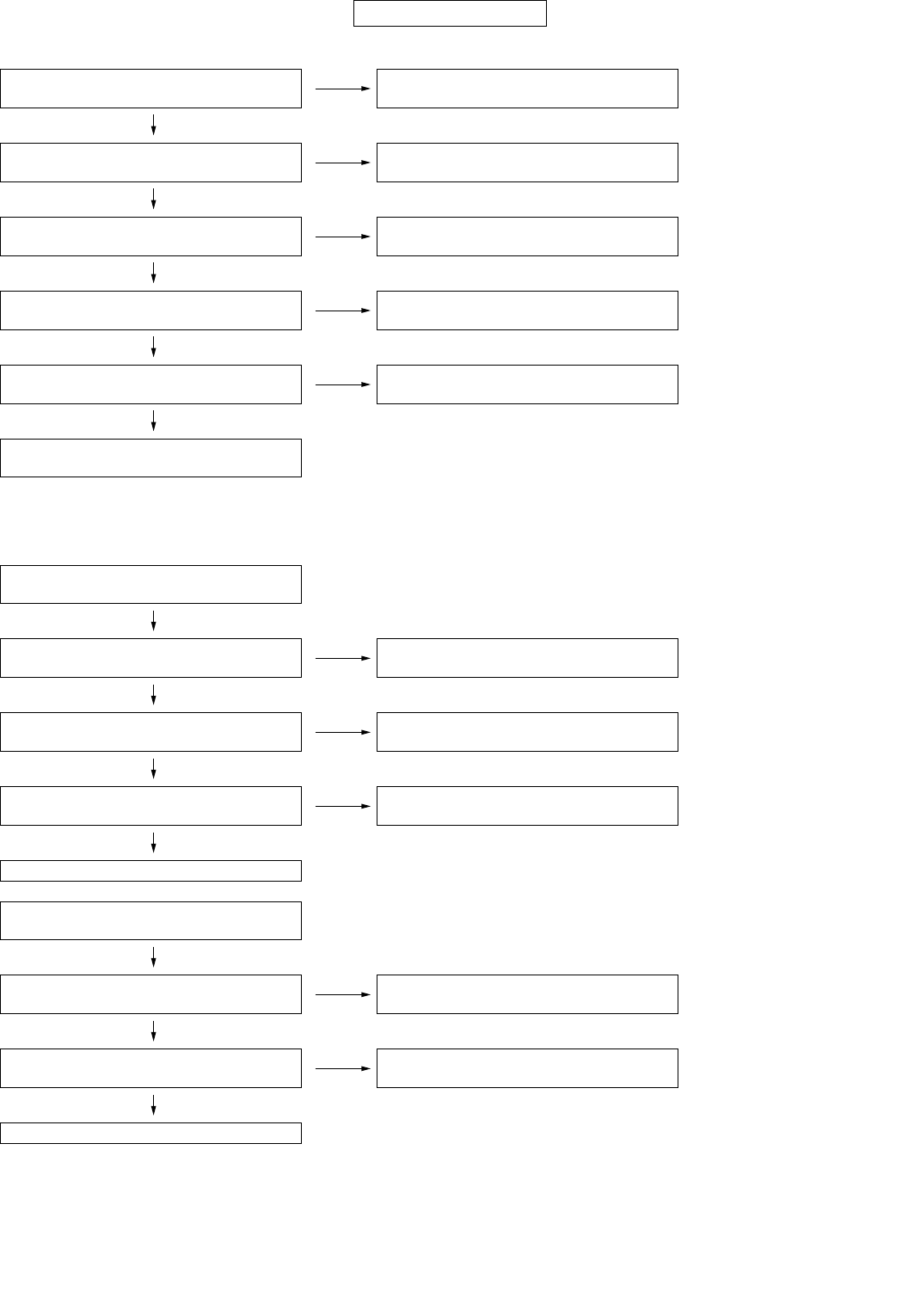
902SH
2 – 40
CONFIDENTIAL
19. USIM card is not recognised.
20. Bluetooth communication is impossible.
Is the USIM card inserted and securely locked? The USIM card is not properly inserted.
Is the USIM card recognised when inserted to a
properly working handset (phone)?
USIM card is defective.
Is “Insert SIM Card” displayed when the power
is turned on without the USIM card?
The software has a problem.
Is the voltage 3.0 V on TP1218 and TP1219? IC1200 is defective.
Does R1232 oscillate? IC1000, IC1200, and R1232 are defective or
mounted improperly.
IC1000, IC1200, R1230, R1231 and R1232 are
defective or mounted improperly.
A connection cannot be established via Blue-
tooth.
Is the voltage approx. 2.9 V applied to TP1021? IC1002 is defective.
TP1022 (RESET signal)always at “High”? IC1000 is defective.
Are pulse signals sent to TP1016
(BT_UARTTX signal)?
IC1000 is defective.
IC1001 is defective.
Phone can be connected to Bluetooth head-
set,but sound is not heard.
Is the signal waveform sent to TP1004 (PCM-
DATB)?
IC1000 is defective.
Is the signal waveform sent to TP1005 (PCM-
DATA)?
IC1001 is defective.
IC1000 is defective. Or IC1001 is defective.
NO
YES
NO
YES
NO
YES
NO
YES
NO
YES
NO
YES
NO
YES
NO
YES
NO
YES
NO
YES
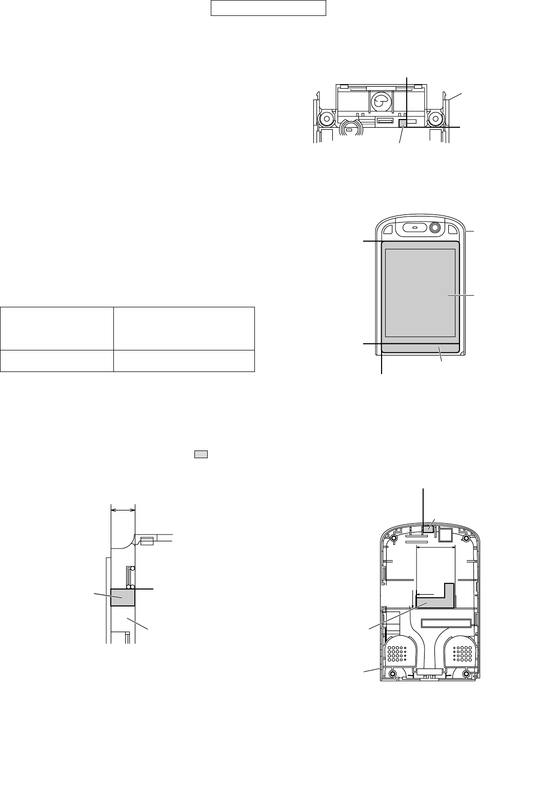
902SH
3 – 1
CONFIDENTIAL
Phone902SHService ManualService ManualMarketE
CHAPTER 3. DISASSEMBLY AND REASSEMBLY
[1] Servicing Concerns
1. For disassembling
1. Do not remove the board of baseband section by pulling external
interface connector not to damage the board.
2. Shield case is attached on shield case holder with no space.
Do not remove together with shield case holder. If you do, you can-
not attach it again because they are soldered and in such a case,
you should take the electric pattern on the board as well.
2. For reassembling
1. Make sure that all ornamental parts have no scratch and clean.
2. Make sure that you can open and close handset (phone) smoothly
and hear hinges click.
3. Make sure that display panel is placed in a proper position without
inclination.
4. Make sure that all three battery terminals protrude evenly.
5. Make sure that the pawl of aerial is upside.
•FASTENING TORQUE (Referential Value)
The reference value is measured when an electric screwdriver
(HIOS CL4000) is used.
•SOLDERING SPECIFICATION
Soldering iron must be set to 380° C for 5 seconds.
•STANDARD POSITION OF ATTACHMENT
When replacing the following labels (marked with ), be sure to
place new ones on the specified positions.
[Sensor, Moisture (Small)]
[Sensor, Moisture (Small)]
[Panel, Main Display/Screw Cover, Display (Bottom)]
[Spacer Cushion, Back Cabinet (Display)/
Sensor, Moisture (Large)]
• Back Cabinet (Key)/
Front Cabinet (Key)
13.8 to 15.7 N • cm
(1.4 to 1.6 Kgf • cm)
• Back Cabinet (Display)/
Front Cabinet (Display)
• Hinge Unit 9.8 to 11.8 N • cm
(1.0 to 1.2 Kgf • cm)
No protrusion
Standard
position
Holder, SD PWB
Sensor, Moisture
(Small)
Sensor Moisture (Small):
Deleted in the middle of October production.
Standard position
Standard position
Front Cabinet
(Key)
Panel,
Main Display
Standard position
Screw Cover, Display (Bottom)
Front Cabinet
(Display)
Standard position
Standard position
Move up to this line.
Attach the cover as
shown (leave no
gap between the
cover and Main
Display panel).
To the left reference position on the
front cabinet (Main Display side).
Spacer Cushion,
Back Cabinet (Display)
Put on
the rib.
Sensor, Moisture (Large):
Deleted in the middle of
October production.
Standard position
Attach within the rib area on the
rear cabinet (Main Display side).
Back Cabinet
(Display)
Standard
position
To the
left
edge
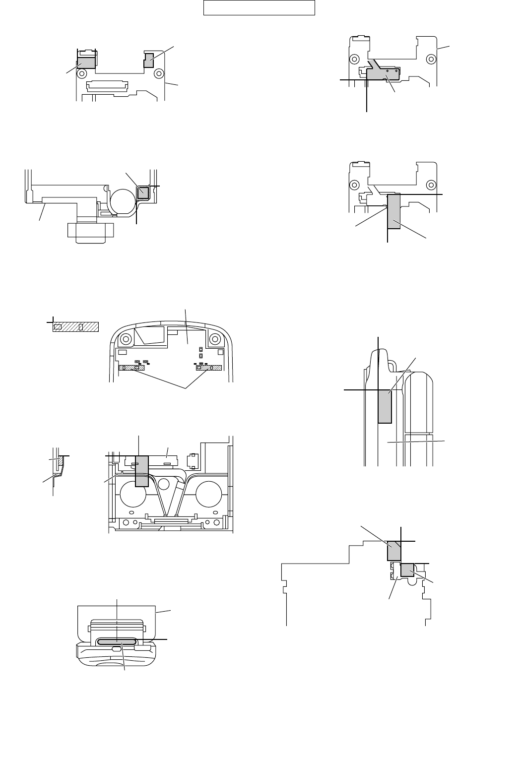
902SH
3 – 2
CONFIDENTIAL
[Holder, Hinge/Cushion, Hinge]
[Cushion, Coaxial Cable]
[Cushion, Display PWB/Kapton, Handling]
[Screw Cover, Side]
[Thin Coaxial (Earth FPC)/FPC Retainer Kapton]
[Label, Qualcomm]
[Kapton, Display PWB/Cushion, LED FPC Unit]
Standard
position
Standard
position
No protrusion
from the PWB
Attach along
the resist line.
Main PWB-A
Holder, Hinge
Cushion, Hinge
Standard position
No contact with the circle
Standard position
Cushion, Coaxial Cable
Holder,
Main PWB
Do not go beyond
the rib. Attach within
the shaded area.
Kapton, Handling
Cushion,
Display PWB
Standard
position
Standard
position
(Left side view)
Connector
Connector
Standard position
Rib Rib
Display PWB-B
Regist
(Attach within the shaded
area.)
Put on the left corner,
without protrusion from
the register.
Standard position
Screw Cover, Side
Front Cabinet,
Hinge
Standard position: Centre
Standard
position
FPC Retainer Kapton
Thin Coaxial (Earth FPC)
Main PWB-A
Do not place on
the BBK shield
case cover. Standard position
To the centre of the marking on
the BBK shield case cover.
No protrusion from the marking.
Standard position
Do not go beyond
the thin coaxial
(flexible earth)
Standard position
To the centre of
the thin coaxial
(Earth FPC)
Do not get into
the cutout area.
Standard
position
Standard position
Label, Qualcomm
Front Cabinet
(Key)
Kapton, Display PWB
Cushion,
LED FPC Unit
Display PWB-B
Standard position
Standard position
Standard position
LED FPC Unit PWB-F Deleted in the
December production.
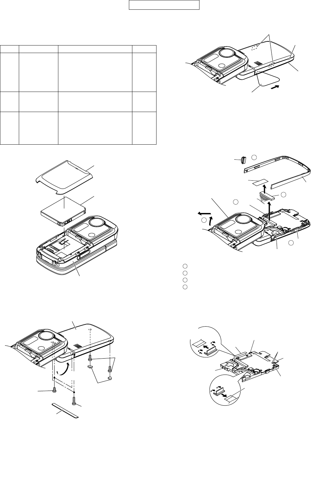
902SH
3 – 3
CONFIDENTIAL
[2] Disassembly and reassembly
• To reassemble, reverse the procedure.
Note that the aerial cover needs to be installed after assembling the
back cabinet (key side).
Figure 1
Figure 2
Figure 3
Figure 4
Figure 5
STEP REMOVAL PROCEDURE FIGURE
1 Back Cabinet
(Display)
Assembly
1.Battery Cover........
2.Li-Ion Battery.........
3.Screw Cover..........
4.Screw....................
5.Hook.....................
(A1)x1
(A2)x1
(A3)x3
(A4)x6
(A5)x2
1
2
3
2 Main Display
Holder Unit
1.Socket...................
2.Hook.....................
(B1)x1
(B2)x2
4
3 Display
PWB-B
1.Solder....................
2.Flat Cable..............
3.Hook.....................
4.Hook.....................
(C1)x2
(C2)x2
(C3)x1
(C4)x1
5
(A1) x 1
(A2) x 1
Back Cabinet (Key)
(A3) x 1
(A4) x 2
M1.4 x 2.8mm
(A4) x 2
M1.7 x 6.0mm
(A4) x 2
M1.7 x 4.5mm,
Black
(A3) x 2
Open
Back Cabinet (Display)
Top belt
(A5) x 2
Insert a jig into the gap between the Top belt and front cabinet
(Main Display side), and slide it to remove the hook A5.
Slide
Front Cabinet
(Display)
Jig
(Use something flat and hard,
for example guitar picks.)
(B2) x 1
(B1) x 1
Top belt
Protect Cover,
Cabinet
Front/Back Cabinet
(Key)
Main Display Holder Unit
Kapton, Handling
Remove the cabinet protection and Top belt.
Remove the handling kapton, and then the socket B1.
Lift and pull off the front/back cabinet (key side).
Remove the hook B2.
1
2
1
2
3
4
3
4
(B2) x 1
4
Display PWB-B
Main Display
Holder Unit
Set it
upright.
(C4)x1*
(C2)x1
(C2)x1
(C3)x1*
(C1)x2
Remove the hook C3,
and then the hook C4.
*
Pull and
set it upright.
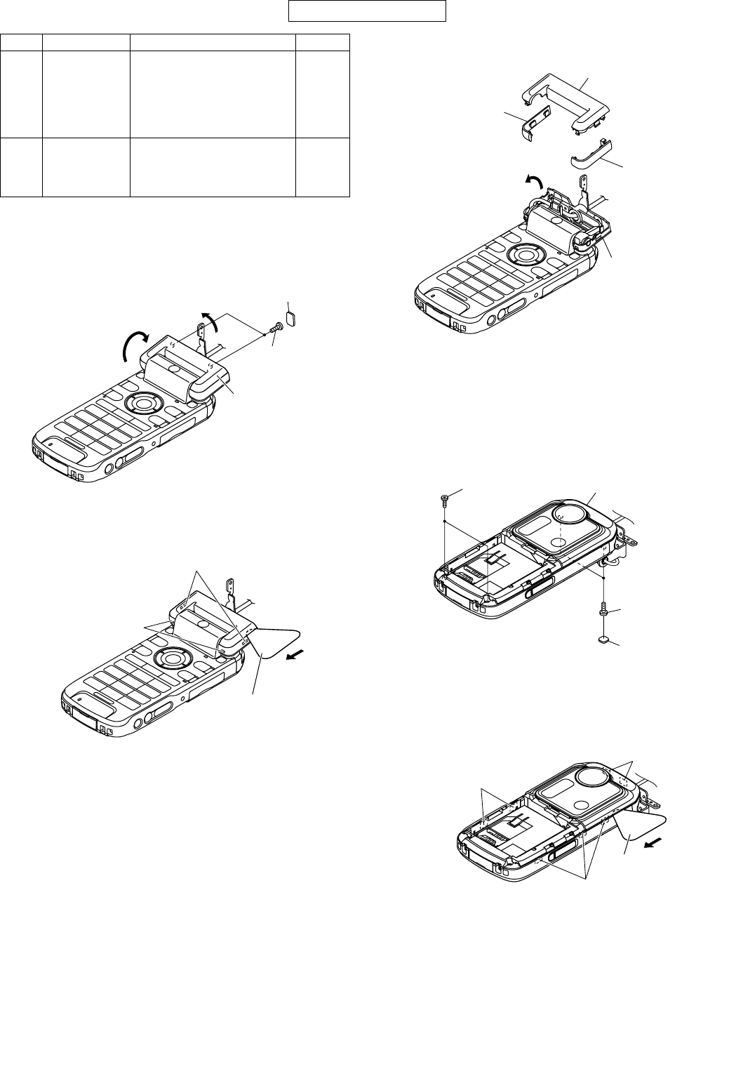
902SH
3 – 4
CONFIDENTIAL
For removal of the hinge unit, refer to “Precautions for installing the
thin coaxial” (3-8).
Figure 6
Figure 7
Figure 8
Figure 9
Figure 10
STEP REMOVAL PROCEDURE FIGURE
4 Hinge Cabinet 1.Screw Cover..........
2.Screw....................
3.Hook.....................
4.Hinge Belt Left......
5.Hinge Belt Right....
(D1)x2
(D2)x2
(D3)x4
(D4)x1
(D5)x1
6
7
8
5 Back Cabinet
(Key)
Assembly
1.Screw Cover..........
2.Screw....................
3.Hook.....................
(E1)x2
(E2)x4
(E3)x7
9
10
(D1)x2
Back Cabinet,
Hinge
(D2)x2
M1.4x2.8mm
Rotate 90
degrees.
Set it
upright.
(D3)x2
(D3)x2
Insert a jig and slide it to remove the hook D3.
Jig
Slide
(D4)x1
(D5)x1
Back Cabinet, Hinge
Front Cabinet, Hinge
*
Set it upright
90 degrees.
* Set it upright as shown and remove the front cabinet (hinge).
(E2)x2
M1.7x5.5mm,
Black
(E2)x2
M1.7x7.5mm
(E1)x2
Back Cabinet (Key)
(E3)x2
(E3)x2
(E3)x3
Slide
Jig
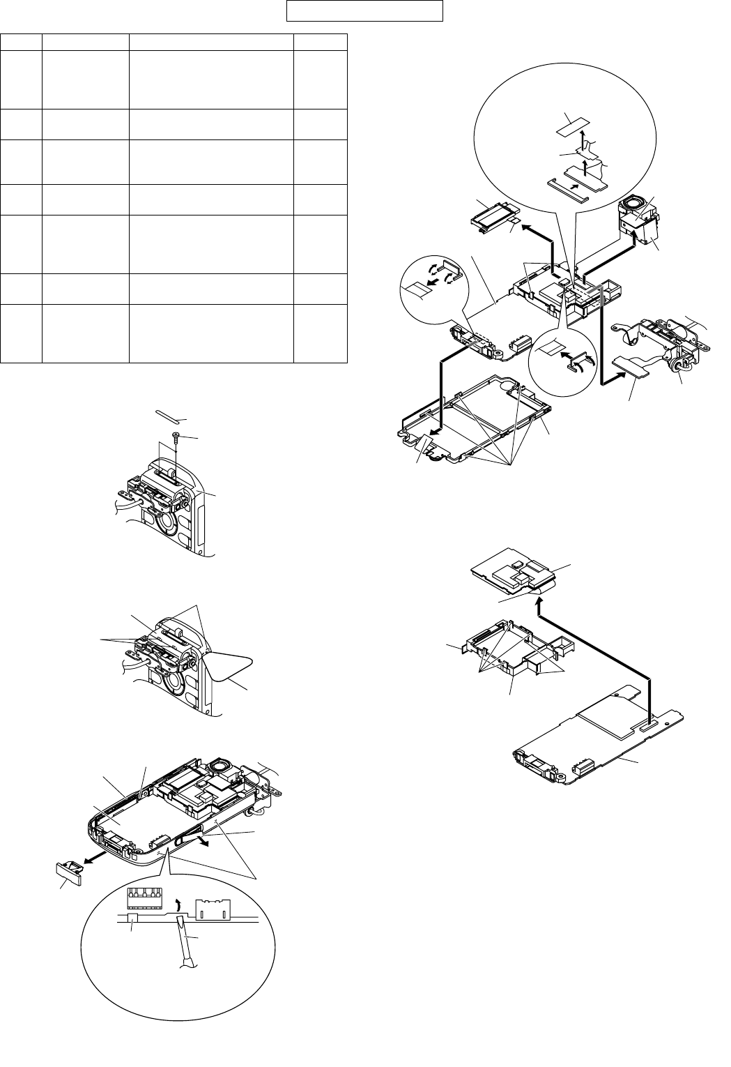
902SH
3 – 5
CONFIDENTIAL
For assembly of the camera, refer to “Assembly procedure for the
camera” (3-7).
Figure 11
Figure 12
Figure 13
Figure 14
Figure 15
STEP REMOVAL PROCEDURE FIGURE
6 Aerial Cover 1.Screw Cover..........
2.Screw....................
3.Hook.....................
(F1)x1
(F2)x2
(F3)x4
11
12
7 Main PWB-A 1.Hook..................... (G1)x3 13
8 Sub Display
Holder Unit
1.Hook.....................
2.Flat Cable..............
(H1)x2
(H2)x1
14
9 Camera
Assembly
1.Socket................... (J1)x1 14
10 Key FPC Unit
PWB-E/
Holder, Main
PWB
1.Hook.....................
2.Flat Cable..............
(K1)x5
(K2)x1
14
11 Hinge Unit 1.Socket................... (L1)x1 14
12 SD PWB-C 1.Hook.....................
2.Socket...................
3.Hook.....................
(M1)x3
(M2)x1
(M3)x4
15
Aerial Cover
(F1)x1
(F2)x2
M1.4x1.6mm
(F3)x2
(F3)x2
Jig
Aerial Cover
(G1)x1
(G1)x2
Cover, External
Connector
Front Cabinet (Key)
Main PWB-A
VIDEO OUT/
Handsfree
Microphone
Connector
Open
Minus
Driver
Hook(G1)
Insert a small flat head screw-
driver and lift off the main PWB-
A to remove the hook G1.
(K2)x1 (K1)x5
(L1)x1
(J1)x1
(H1)x2
(H2)x1
Sub Display
Holder Unit
Camera
Assembly
Key FPC Unit PWB-E/
Holder, Main PWB
Main
PWB-A
Hinge Unit
Set it
upright.
Set it
upright.
Thin Coaxial
(Earth FPC)
Remove the FPC
retainer kapton.
(M2)x1
(M3)x4 (M1)x2
(M1)x1
Main PWB-A
SD PWB-C
Holder, SD PWB
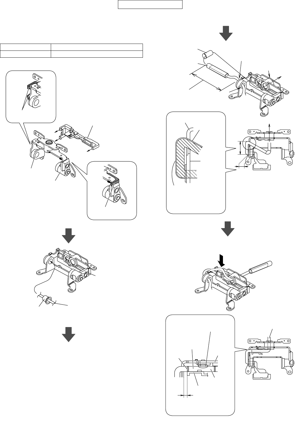
902SH
3 – 6
CONFIDENTIAL
[3] Precautions for installing the thin coax-
ial
Attach the connector cover before installing the thin coaxial.
After the installation, leave the connector cover off.
Part Code Description
PCOVPA003AFZZ Cover, Connector
Hinge Unit
Blue
Wire Holder B
Fix Holder, Hinge
Hole B
Hinge Unit
Fit the hooks of the
hinge holder.
Fit the hooks of the
hinge holder.
The thin coaxial connector
should be routed through the
wire holders A and B
beforehand.
Holder, Hinge
Hole A
Hole B
Hinge Unit
Cover,
Connector
Thin Coaxial
(Earth FPC)
Thin Coaxial
(Cable)
a
b
A
Thin Coaxial
Fix the "A" part and bend the
thin coaxial into an N shape to
insert the hole A. This prevents
twisting of the thin coaxial (ca-
ble/earth FPC).
Hinge Unit
Earth FPC
When routing through the hole
B, straighten the thin coaxial and
continue to make arcs with it.
Sagging must be
out of the hole B.
Position the thin coaxial
(earth FPC) outside the
thin coaxial (cable). Pay
special attention to the
sections "a" and "b".
Adjusting the length, insert the
thin coaxial into the hinge holder.
The earth FPC must
be in contact with the
hinge unit.
Nitoflon
overlap
area
End face
of the
earth
FPC
The end face of the
earth FPC
must be within this range.
(Keep it inside the hinge.)
Yellow
Wire Holder A

902SH
3 – 7
CONFIDENTIAL
– MEMO –
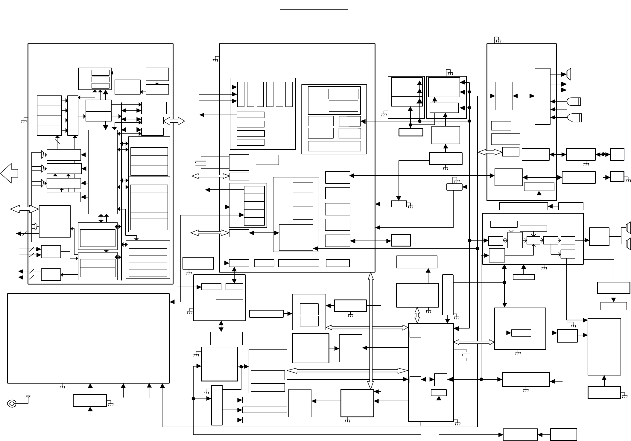
CONFIDENTIAL
4
--
1 4
--
2
Figure 1 MAIN BLOCK DIAGRAM
CHAPTER 4. DIAGRAMS
[1] Block diagram
902SH 902SH
Rake
Fingers
Rake
Fingers
Rake
Fingers
Rake
Fingers
DSP
RRMA
RAM
DPL L
EMI F
Combiner
TFCI
decorder
IO-Bus
System
Cont APLL
Clock
square
HSSL
Sleep
Contlor
UART
HSSL
Memory
Controller
3wire
Serial bus
To IC400/
IC700
RXIA/IB
RXQA/QB
TXI/IBAR
TXQ/QBAR
To
IC1200
DAC BUS
To RF Block
20, 23, 24,
27, 34, 41,
45, 48, 67,
70, 83, 87,
94, 104, 109,
120, 127, 135,
138, 139, 156,
179, 181
126, 145
144, 160
124, 174
142, 173
A/D
D/A
RF-I/F
AGC
Pow
Control
TIMING
Generator
Code
Generator
Path
Searcher
Cell
Searcher
Interleaver
Rate
Matching
TX-Stage2
TX-Stage3
Waveform
Gen
Interleaver
Turbo Coder
Viterbi Coder
CRC
Ciphering
TX-Stage1
De-interleaver
Rate dematching
Viterbi Decorder
Turbo Decoder
CRC
De-ciphering
RX-Stage2
De-interleaver
Phys.CH
Transport.C
De-seg H
De-multiplex
RX-Stage1
CH Codec
IC1001
BGB202
BLUETOOTH
CN061
2.9 V
REGULATOR
IC1002
R1162D291D
BATT+B : 4.0V
BLUETOOTH
AERIAL
MCK RTCCLK
PCM
EXTERNAL
CONNECTOR CN1300
SUB BACKLIGHT
MOBILE LIGHT LED
MAIN BACKLIGHT
REGULATOR
CAMERA
(2MPixel)
CAM Cont
CCD sensor
LVD S
MAIN
DISPLAY
LCD3000
DISPLAY
CONTROLLER
I2C
SIO
SIO
IC3000
LR38866
T4C
PLL
IC2003
BD6030
COMPOUND
POWER
SUPPLY 3
IC2004
XC640231
IC1500
TC3525XBG
MULTIMEDIA
ACCELERATOR
SDI/F
LVD S
PCM
I/F PCM
IC1300
BU7880GU
EXTERNAL
INTERFACE
UART USB
Handsfree
MCPC MUX
IC1303
XC6219C332DR
X1000
32.768KHz
I2C
HSSL
IDATA
QDATA
DCLK
From
IC101
MOD
[A-D]
3.3 V
REGULATOR
JK1600
VIDEO OUT/
HANDSFREE
MICROPHONE
CONNECTOR
I2C
RTC TIMER
RXIF
EQU
NODI
4 x CHD
DIRMOD
SERCON
CLKCON
TIMGEN
CRYPTO
FCHDET
GSM/GPRS
GPIO
UART0
UART1
UART2
UART3
UART4
HSSL
USB I/F CAM I/F IrDALCD I/F
SYS
CONTROL
KEYPAD
SIM I/F
INTCON
MMC
SARAM
DARAM
ROM
DSP
LEAD3
Speech Codec
Audio
Algorithm
etc
IC1000
D751668AZZG
BASEBAND
MANAGEMENT
CPU
BOOT
ROM EMIF
ARM946E
RAM
RAM
DMA
Interconnect Matrix
SUB CAMERA
CAM
Cont
CCD
sensor
2.9V
REGULATOR
REGULATOR
IC3001
R1162D291D
IC3004
R1162D251D
I2C I2C
I2C
IC1504
FA3727R
PCM
KEY
MATRIX
PSRAM
(64Mbit)
PSRAM
(128Mbit)
IC1100
LHF65NZ1
FRASHMEMORY1
IC1101
MB82R6A5C
FRASHMEMORY2
BAT1200
BACK-UP
BATTERY
1.8V
REGULATOR
IC1206
R1163D181B
1.8V
IC1200
TWL93004CZQW
POWER SUPPLY
/RF CONTROL
1.5V
1.5V
2.9V
REGULATOR
IC1205
S-817A15APF
POWER SUPPLY
IC1205
S-817A15APF
POWER SUPPLY
IC1204
S-817A15APF
POWER SUPPLY
SRAM
(8Mbit)
FLASH
(128Mbit)
FLASH
(256Mbit)
FLASH
(256Mbit)
I2C
PCM
BATTERY TERMINALCN1200 BATTERY BATT+B : 4.0V
Audio
I/F
IC1200
TWL93004CZQW
POWER SUPPLY
/RF CONTROL
SIM
Level
sift
Charger
Control
OSC
Sleep
Con
I2C
LDOA/B/D
PCM
I/F MIC
To HP Receiver
MIC200
EP1000
EARPIECE
To PCM CODEC
From HP MIC
MIC201
MIC
SIM
CONNECTOR
CHARGER
CIRCUIT
CN1201
IC1202
TK73840BDB
REGULATOR AC CHARGER
2.0V
IC1201
XC61CC20C2NR
VOLTAGE DETECTOR
MA5
IC1600
YMU783C
MOBILE
AUDIO
I/F
ADPCM
LOGIC
DA MIX
FM
SY
N
AMP
PCM
I/F AMP
PCM
SP2000
SPEAKER
SP2001
SPEAKER
AGC
STEREO
AMP.
IC1603
AN12974A
VIBRATOR
VIBRATOR
REGULATOR
VIB001
IC1601
BH30FB1WHFV
1.8V
IC1200
TWL93004CZQW
POWER SUPPLY
/RF CONTROL
SD CARD
CONNECTOR
CN2001
SD POWER
CONTROL
IC2001
R1161D291D
PCM
CODEC
IC1700
AK4569
From
IC1200
PCM
IC1602
R1163D291B
JK1600
VIDEO OUT/
HANDSFREE
MICROPHONE
CONNECTOR
2.9V
IC1400
D751980CZPH
W-CDMA MODEM
4
2, 5
3
12, 13,
28, 43
2, 5
2
12, 28
5, 7
3130
163~166
220,
260
238,
258
246
226
75, 83,
84, 123
133
144
132
2, 13, 66~69, 76, 77,
86, 92, 94, 95, 108,
138, 143, 148, 154,
191, 193, 212, 223,
227, 233, 229, 244,
248,271, 276, 284
183, 230, 231,
250~253, 270,
272, 285, 286
218, 236
8, 16,
77, 78,
81~84
169~171
56, 82
9, 10,
74, 80 58
121
3
3
5
3
2
283
196
3
10
3, 11, 25
111, 112, 117,
125, 127, 139,
172, 177,
206~208, 235,
236, 240, 242,
314, 334
32, 50,
51, 68
54~56, 59, 61, 69, 76, 85, 92,
101, 108, 116, 118, 120, 122
11, 12, 23 5
5
3
4
1
18, 28, 56,
64, 69
50
10
48,
54
28,
30
10, 12,
13, 15
4
2
5, 6
8, 9
71
84,
85,
98 61, 72,
73, 86
38,
39,
49
139
138
122,
135
30, 42~44, 52~58, 64~68, 75~80,
88~92, 111, 112, 115,
2
2
5
8, 9
SUB
DISPLAY
LCD2000
IC2005
BD6015GU
COMPOUND
POWER
SUPPLY 1
POWER CONTROL
INFRARED
REMOTE
Tx CONTROLLER
LSI
IC1502
BU7876GL
LED1503
INFRARED PORT
Encode
29~31
I2C
IC1800
AK8813P
NTSC ENCODER
10, 12, 15,
28, 35, 48, 51
17, 18
3
5
55
X1500
27MHz
200
279,
296
213
VIDEO
AMP
IC1701
MM1671XN
42
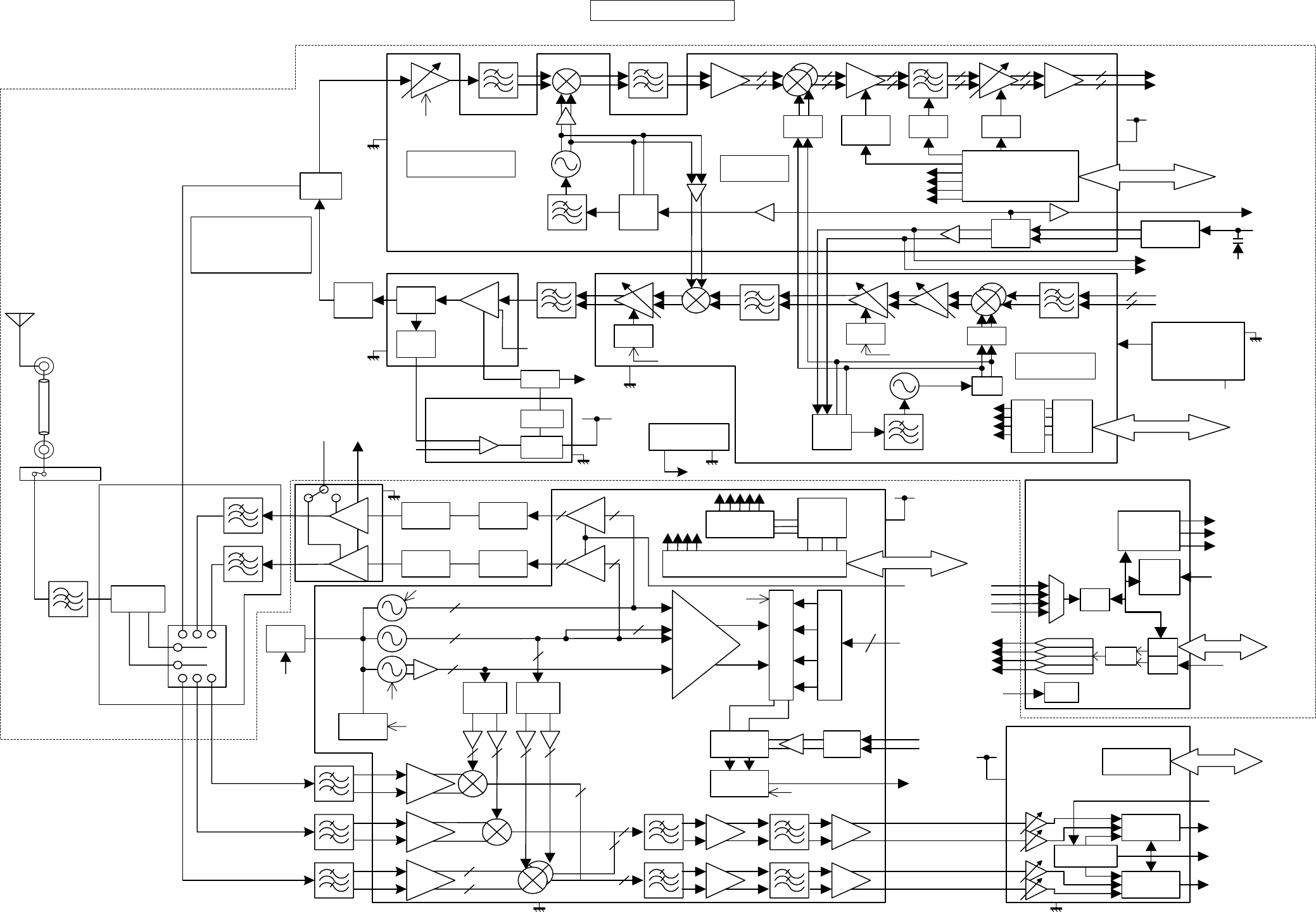
CONFIDENTIAL
4
--
3 4
--
4
Figure 2 RF BLOCK DIAGRAM
902SH 902SH
TRANSMITTER
fTx: 1922.6~1977.4MHz
RECEIVER
fRx: 2112.6~2167.4MHz
CPL
TEMPERATURE
SENSOR
RF
PLL
VCO TUNE
RF VCO
ISO-
LATOR
DET π/2 0
IF
PLL
IF VCO
1520MHz
Rx SERIAL IF
Tx
SERIAL
IF
MCPC_I/F
2ndLO
fL2:760MHz
RXIA/RXIB
RXQA/RXQB
TXI/TXIBAR
TXQ/TXQBAR
fIF_Tx=380MHz
GLNA
RXON
PLLCTRL
MCLK
XO
TXRFVGA
TXIFVGA
VCXOCTRL
PLLCTRL
TXRFVGA
VGA
CTRL
VGA
CTRL
LPF
TUNE
GAIN
TOL.
KILLER
TXIFVGA
FILTER
SWITCH
PWM
/PFM
DAC1 REF
FB
VBAT
LX
DAC4
LOGIC
DIV
90 0
DIV
90 0
GSM (900MHz)
LOOP
FILTER
HYBRID
BALUN
897.5MHz
HYBRID
BALUN
1.810MHz
ATT
ATT
DELAY
VCO
TEST
DCS (1800MHz)
PCS (1900MHz)
PHD
CHARGE
PUMP
XO
PHDOUT
PHDOUT
BUSINTERFACE
CURR.REQ.
SIGMA
DELTA
SIGMA
DELTA
CLOCK
SQUARER
I2C SERIAL
CONTROL
LOGIC
VTUNE
MOD[A-D]
Rx VCO High
(4G)
Tx High Rx Low (2G)
Tx VCO Low (1G)
RFHA
RFHB
RFHC
RFHD
RFLA
RFLB
PCTL
PRESCALER
IRA
IRB
QRA
QRB
IDATA
QDATA
DAC2
I2C
DCLK
SYSCLK2
IPOS
INEG
QPOS
QNEG
XOOB
XOOC
13MHz
DIPLEXER
1/2
1/2
DAC3
FL002
DUP-
LEXER
FL400 FL420
IC400
OM5954ET
RECEIVER IC FOR W-CDMA
X770
FL001
ANT SW
MODULE
IC620
MAX1820XEBC
DC/DC
FL650
IC630
RF9266
W-CDMA POWER AMP.
IC700
OM5955ET
W-CDMA
TRANSMIT-
TER IC
CN1300
EXTERNAL
CONNEC-
TOR
IC501
LM20SITLX
IC300
CX77313
POWER AMP.
MODULE (FOR GSM)
FL330
FL331
IC100
OM5952AET
RECEIVER/
TRANSMISSION IC
FOR GSM
FL100
RX-SAW
FL120
RX-SAW
FL110
RX-SAW
IC101
AB1011
GSM CODEC
IC800
LP3981ILD
2.8 V
REGULATOR
IC1200
TWL93004CZQW
POWER
SUPPLY
/RF CONTROL
CRYSTAL
13MHz
GPA0
GPA3
FL500
8bit DAC
11bit DAC
8bit DAC
8bit DAC
MCLK
VDD_B
LDO
VDD_A
LDOA
LDOB
LDOD
1MHz
OSC
GPADC
I2C
M
U
X
GP
ADC
DAC01
DAC02
DAC03
DAC04
PA
CONT
GPA0
GPA2
GPA3
GPA4
XOOC
XOOB
BUILT-IN
AERIAL
To IC1000
To IC1000
From IC1000
IF BPF
13MHz
D770
GLNA
2ndLO
fL2: 760MHz
1stLO
fL1: 2302.6~2357.4MHz
Rx_IF AMP
fIF_Rx=190MHz Rx LPF Rx AGC AMP
CN901
Tx LPF
From IC1000
[W-CDMA RF]
[GSM RF]
DAC BUS
From IC1400
From IC1400
From IC1400
To IC1400
From IC1400
REG
To IC1000
I2C
VCCPA
VDD_B
VDD_D
VDD_D
VDD_A
3WIRE SERIAL BUS
3WIRE SERIAL BUS
3WIRE SERIAL BUS
I/QDEM
I/QMOD
LNA
FL003
ESD DEVICE
CN902
COAXIAL CABLE
VCCPA
PA
π/2 0
1/4
13
44
21
2
3, 11, 12, 14, 19, 23, 25, 27,
28, 31, 32, 38, 39, 41, 43
1
5
4
11
+B
13
9
37
2, 27, 29
31, 33, 40~45
48
1
5
10
8
31, 8
5, 6, 10
4
7, 15, 16
18, 19
21 48
49
9, 14, 16, 17, 19, 20,
22~24, 30, 31, 34,
38~42, 43, 46, 50
36 32
29 25
29, 33
45, 47
3, 6, 9,
11~14, 17
20, 22, 23
7, 8, 10, 12
14, 15, 17
1, 9, 17, 18, 20, 28, 39, 40,
46, 47, 51, 52, 54, 63, 64
7
8
9
10
46
55
54
49~52
34
141
117
130
118
17
82
94
83
2, 13, 15,
45, 48, 62
8
7
6
529
21
4
56
25, 27
21, 32
116
142
11
24
9, 10
7, 8
18
4, 3
1, 2
8, 10, 28
33, 36, 44
24
20
2319
46
56
37
45
4, 7
7
32
2
+B
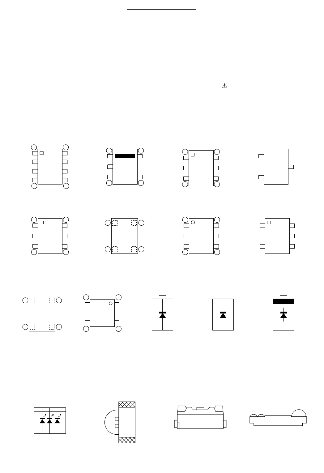
902SH
5 – 1
CONFIDENTIAL
Phone902SHService ManualService ManualMarketE
CHAPTER 5. SCHEMATIC DIAGRAM AND WIRING SIDE OF P.W.BOARD
[1] Notes on schematic diagram
•Resistor:
Letters K and M are prefixed to ohm (unit of resistance).
K means 1000 ohms and M means 1000 kohms.
• Capacitor:
P is an abbreviation for “pico” and a farad (unit of capacitance)
without P means “microfarad”. Expressions “capacitance/withstand
voltage” are used for electrolytic capacitors.
(CH), (RH), (UJ): Temperature compensation
(ML): Mylar type
(S): Styrol type
(PP): Polypropylene type
• The voltage of each section is obtained by measuring between the
section and chassis using a digital multimeter [handset (phone) out
of range].
• Conditions: SIM card inserted, power on, in stand-by mode
(opened)
• Schematic diagram and Wiring Side of P.W. Board for this model
are subject to change for improvement without prior notice.
• Parts marked with “ ” are important for maintaining the safety of
the set. Be sure to replace these parts with specified ones for main-
taining the safety and performance of the set.
[2] Types of transistor and LED
TOP VIEW
1SS389F
RB520S30
RB521G30
RB521S30
RB551V30
BBY58-02V
B
(3)
(G) C
(2)
(D)
E
(1)
(S)
DTC114 YM
DTC123 EM
TOP
VIEW
RN47A4 JEF
E1
B1
E2
C1,B2
C2
TOP
VIEW
1
3
5
4
1
(D)
3
(D)
2
(G)
2
(D)
3
(D)
1
(S)
TOP
VIEW
1
3
6
4
MCH6413
EMT1
1
(E)
3
(B)
2
(C)
2
(C)
3
(B)
1
(E)
TOP
VIEW
1
3
6
4
HN1C03 FUZ
1
(D)
2
(D)
3
(G)
6
(D)
5
(D)
4
(S)
TOP
VIEW
1
3
6
4
SCH1302
SI1555 DL
EC4404 C
G
S
D
D
TOP
VIEW
1
2
4
3
EC3201 C
C
C
B
E
TOP
VIEW
4
3
1
2
1
(E)
2
(B)
3
(C)
6
(C)
5
(B)
4
(E)
TOP
VIEW
FDG312 P
TOP VIEW
NECW008A
123
654
GM56281A
TOP VIEW TOP VIEW
BRPY121F
TOP
VIEW
ECH8603
2
(D)
1
(D)
1
(D)
2
(D)
1
4
8
5
2
(G)
1
(S)
1
(G)
2
(S)
TOP VIEW
CUS02Z
SB0503EJ
TOP VIEW
SB0203EJ
TOP VIEW
GP2W3240
TOP
VIEW
EC4301 C
EC4401 C
1
2
4
3
G
S
D
D
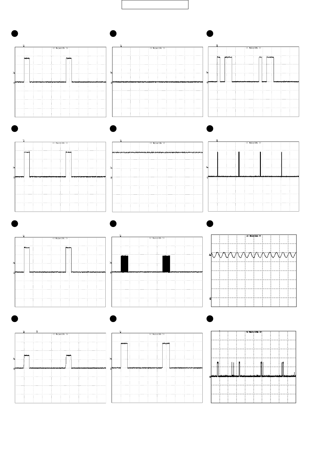
902SH
5 – 2
CONFIDENTIAL
[3] Waveforms of circuit
1C001 EGSM (Talking)
(CH1=1V, 1ms/div)
2C002 DCS (Talking)
(CH1=1V, 1ms/div)
3C003 DCS (Talking)
(CH1=1V, 1ms/div)
4C327 EGSM/DCS/PCS (Talking)
(CH1=1V, 1ms/div)
5C331 EGSM (Talking)
(CH1=1V, 1ms/div)
9
SP032 EGSM·DCS·PCS (Stand-by)
(CH1=1V, 1ms/div)
6C331 DCS/PCS (Talking)
(CH1=1V, 1ms/div)
10
SP032 EGSM·DCS·PCS (Out-of-range)
(CH1=1V, 200ms/div)
7
R213 (IC2100 side) EGSM/DCS/PCS (Talking)
(CH1=1V, 1ms/div)
8SP031 EGSM/DCS/PCS (Talking)
(CH1=1V, 1ms/div)
11
R760 MCLK (13MHz)
(CH1=500mV,100ns/div)
12
TP1023 RF_CLKREQ (
Stand-by
)
(CH1=1V, 1s/div)
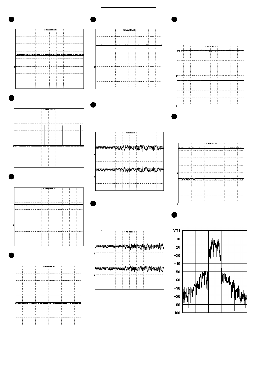
902SH
5 – 3
CONFIDENTIAL
13
TP1023 RF_CLKREQ (Talking)
(CH1=1V, 1s/div)
14
SP023 RX_ON (Stand-by)
(CH1=1V, 1s/div)
15
SP023 RX_ON (Talking)
(CH1=1V, 1s/div)
16
SP029 TX_ON (Stand-by)
(CH1=1V, 1s/div)
17
SP029 TX_ON (Talking)
(CH1=1V, 1s/div)
21
SP003
TXQA
(Transmitting W-CDMA modulated waves)
SP004
TXQB
(Transmitting W-CDMA modulated waves)
(CH1, CH2=200mV, 10µs/div)
18
SP015
RXIA
(Receiving W-CDMA modulated waves)
SP016
RXIB
(Receiving W-CDMA modulated waves)
(CH1, CH2=200mV, 5µs/div)
22
CN1300 (RF output)
(9862ch, Pout=23dBm)
19
SP017
RXQA
(Receiving W-CDMA modulated waves)
SP018
RXQB
(Receiving W-CDMA modulated waves)
(CH1, CH2=200mV, 5µs/div)
20
SP001
TXIA
(Transmitting W-CDMA modulated waves)
SP002
TXIB
(Transmitting W-CDMA modulated waves)
(CH1, CH2=200mV, 10µs/div)
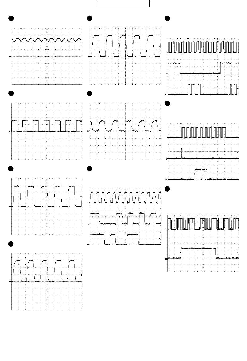
902SH
5 – 4
CONFIDENTIAL
25
TP1014 SYSCLK1 (Display is turned on)
(CH1=1V, 40ns/div)
26
R1517 LCDCLK (Display is turned on)
(CH1=1V, 80ns/div)
27
R1522 CAMCLK (Camera is active)
(CH1=1V, 80ns/div)
TP1221 SIMCLK
(Accessing SIM after power-on)
TP1220 SIMDAT
(Accessing SIM after power-on)
(CH1, CH2=2V, 2µs/div)
28
TP1800 BECLK (Sending video call image)
(CH1=2V, 20ns/div)
29
R1533 SDCLK (Playing Music)
R1532 SDDATA0 (Playing Music)
R1528 SDCMD (Playing Music)
(CH1, CH2, CH3=2V, 80ns/div)
31
R1058 PCMCLK (Talking)
R1057 PCMSYN (Talking)
R1025 PCMDATA (Talking)
(CH1, CH2, CH3=2V, 10µs/div)
30
R1572 BICK (Playing Music)
R1571 LRCK (Playing Music)
R1565 ADSDO (Playing Music)
(CH1, CH2, CH3=2V, 2µs/div)
23
C1031 MCLK (Talking)
(CH1=1V, 80ns/div)
24
TP1006 RTCCLK (Power ON)
(CH1=1V, 20µs/div)
32
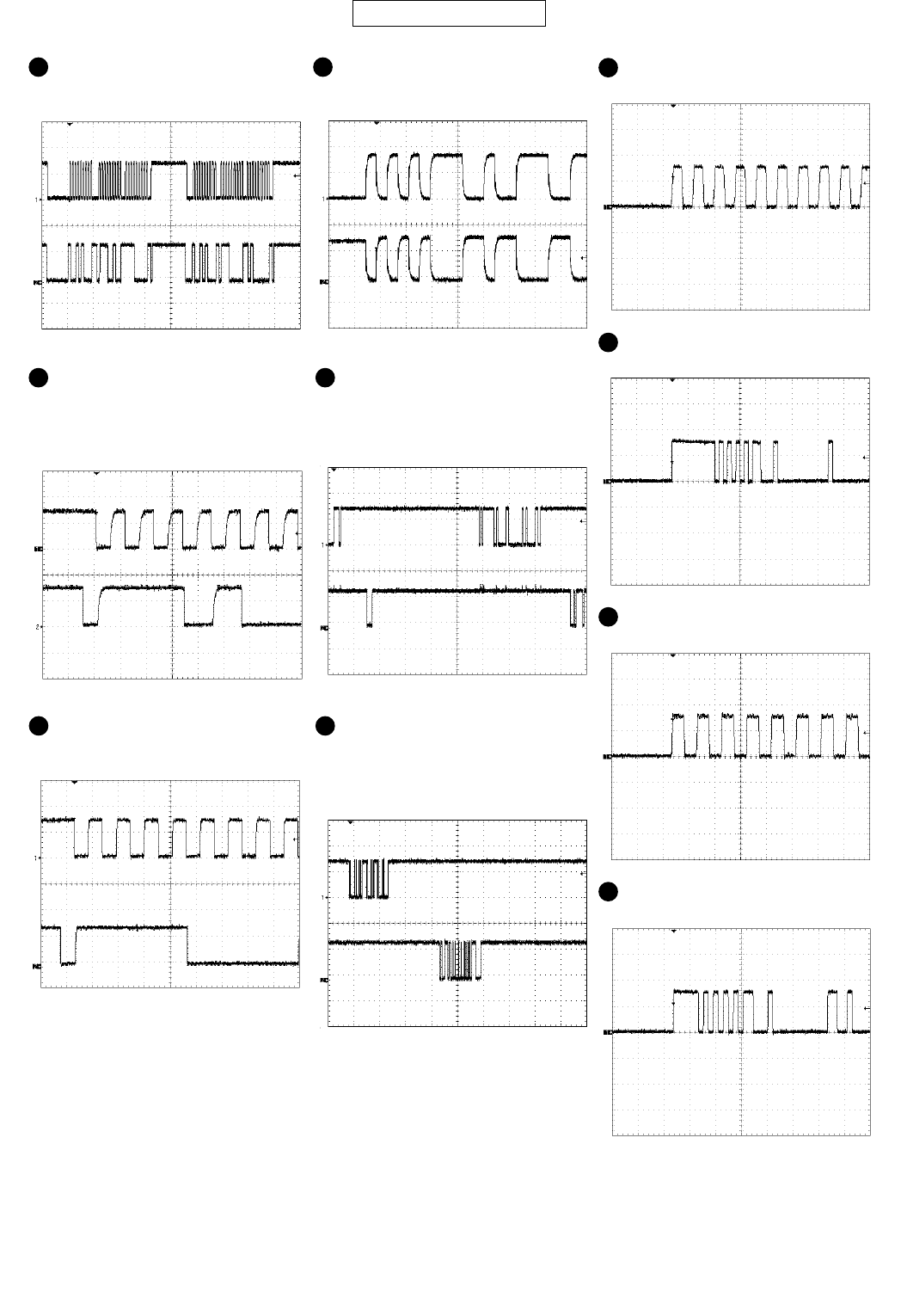
902SH
5 – 5
CONFIDENTIAL
35
R1542 I2CDATB (Camera is active)
R1543 I2CCLKB (Camera is active)
(CH1, CH2=2V, 4µs/div)
36
TP1305 USBDM (Connected to PC)
TP1306 USBDP (Connected to PC)
(CH1, CH2=2V, 200ns/div)
37
TP1613 UARTOTX
(Display remote is active)
TP1614 UARTORX
(Display remote is active)
(CH1, CH2=2V, 1ms/div)
38
TP1016 BT_UARTTX
(Turning on the power)
TP1015 BT_UARTRX
(Turning on the power)
(CH1, CH2=2V, 400µs/div)
39
RA1018 HSSLTXCLK (Talking)
(CH1=1V, 80ns/div)
40
RA1018 HSSLTX (Talking)
(CH1=1V, 400ns/div)
42
RA1018 HSSLRX (Talking)
(CH1=1V, 400ns/div)
41
RA1018 HSSLRXCLK (Talking)
(CH1=1V, 80ns/div)
33
R1041 M_I2CCLK (Display is turned on)
R1042 M_I2CDAT (Display is turned on)
(CH1, CH2=2V, 2µs/div)
34
R1544 I2CDATA
(Video call: Sub camera is active)
R1545 I2CCLKA
(Video call: Sub camera is active)
(CH1, CH2=2V, 4µs/div)
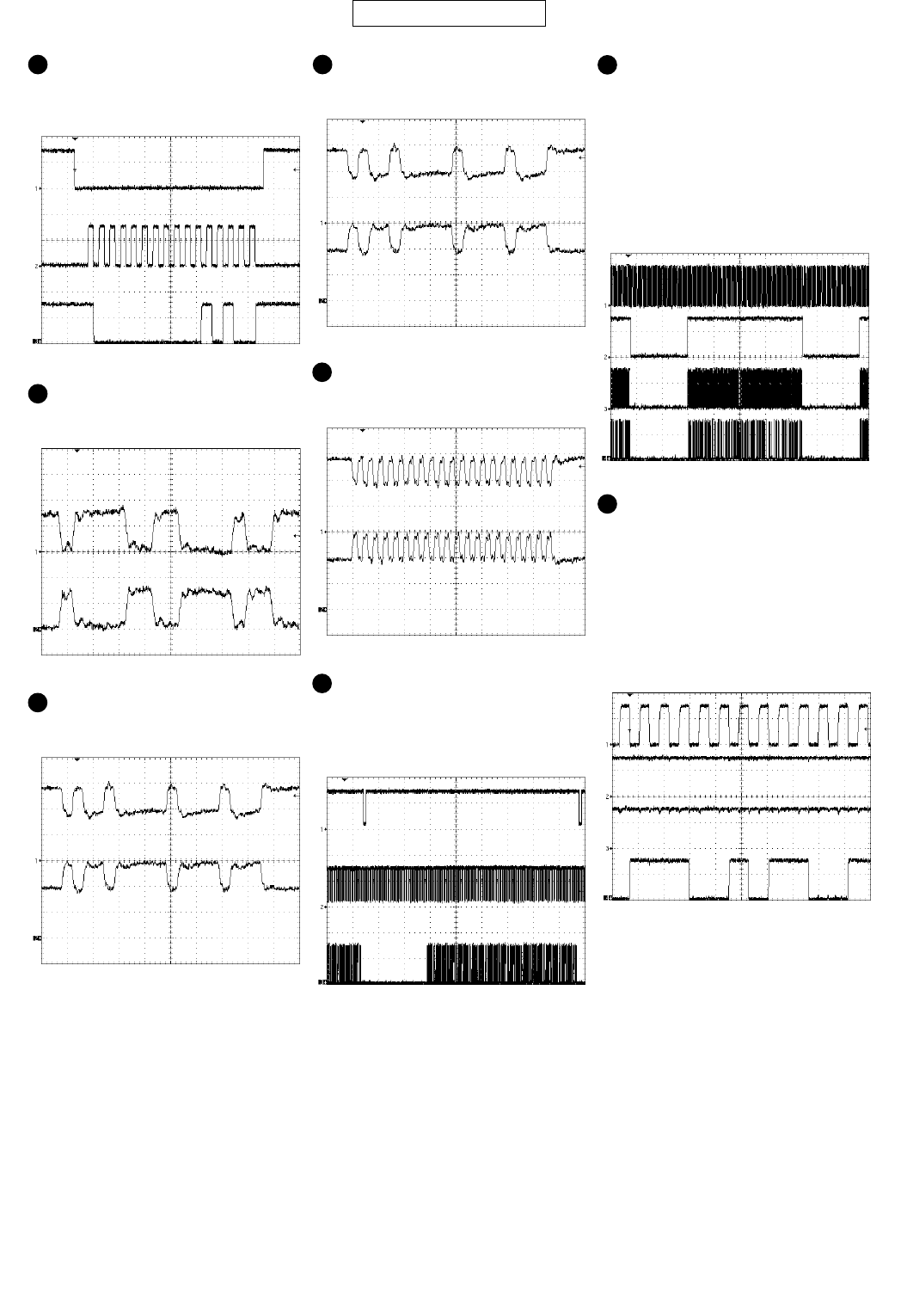
902SH
5 – 6
CONFIDENTIAL
47
L3011
VTX1CKP (Display is turned on)
L3012
VTX1CKN (Display is turned on)
(CH1, CH2=500mV, 20ns/div)
48
RA1800 BEVSYNC
(Sending video call image)
RA1800 BEHSYNC
(Sending video call image)
(CH1, CH2, CH3=2V, 2ms/div)
49
Pressure-welded flexible PWB of sub camera
PCLK
(During video call, with sub camera active)
VSYNC
(During video call, with sub camera active)
HSYNC
(During video call, with sub camera active)
D0
(During video call, with sub camera active)
(CH1, CH2, CH3, CH4=2V, 10ms/div)
50
Pressure-welded flexible PWB of sub camera
PCLK
(During video call, with sub camera active)
VSYNC
(During video call, with sub camera active)
HSYNC
(During video call, with sub camera active)
D0
(During video call, with sub camera active)
(CH1, CH2, CH3, CH4=2V, 400ns/div)
45
C1554 VRX2CKP (Camera is active)
C1554 VRX2CKN (Camera is active)
(CH1, CH2=100mV, 20ns/div)
46
L3009
VTX1DP (Display is turned on)
L3010
VTX1DN (Display is turned on)
(CH1, CH2=500mV, 20ns/div)
R1506
LEDLD (Backlight ON: Key is pressed)
R1503
SECLK (Backlight ON: Key is pressed)
R1504
SEDO (Backlight ON: Key is pressed)
(CH1, CH2, CH3=2V, 1µs/div)
43
C1555 VRX2DP (Camera is active)
C1555 VRX2DN (Camera is active)
(CH1, CH2=100mV, 20ns/div)
44
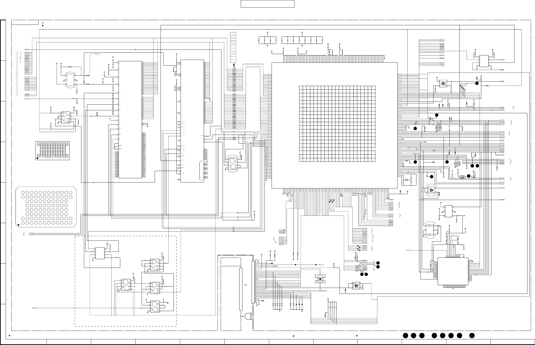
CONFIDENTIAL
5
--
7 5
--
8
Figure 1 SCHEMATIC DIAGRAM (1/9)
902SH 902SH
A
B
C
D
E
F
G
H
12345 6789
10 11 12
NOTES ON SCHEMATIC DIAGRAM can be found on page 5-1. Waveform numbers of
12
to,
13
,
4238
to
2523
,
31
,,
33
are shown on pages 5-2 to 5-5.( ) : Not Mount
[4] Schematic diagram/Wiring side of P.W.Board
MAIN PWB-A(1/6)
NC
NC
NC
NC
NC
NC
NC
NC
NC
NC
NC
NC
NC
NC
NC
NC
NC
NC
NC
NC
NC
NC
NC
NC
NC
NC
NC
NC
NC
NC
NC
NC
NC
NC
NC
NC
NC
,
13
12
41
38
31
23
24
31
4042
39
33
25
MODB
MODD
MODA
MODC
PCTL
ANTSW2
RXON
ANTSW1
ANTSW0
TXON
RADSTR
RADDAT
RADCLK
BSEL0
ISSYNC
ISEVENT
PWRREQ_N
PWRRST_N
ONSWC
ADCSTR
DACSTR
DACCLK
DACDAT
RTCCLK
RESOUT1_N
RESOUT0_N
ANTSW3
TDO
TRST_N
TMS
TCK
TDI
RESHERTA
QDATA
DCLK
IDATA
HSSLRXCLK
HSSLRX
HSSLTX
HSSLTXCLK
HIFIDET_N
T4G_PLLLD_N
T4G_PLLEN
FLIP_R
UARTSENSE
CAMINT
SERVICE_N
JACKDET_N
JACKPOWEN
ONSWPUEN
SYSCLK2
RF_CLKREQ
CLKREQ
NC
NC
NC
NC
NC
NC
NC
NC
NC
NC
NC
NC
NC
NC
NC
NC
NC
NC
NC
NC
PWRRST_N
NC
NC
VMEM18
NC
NC
NC
NC
NC
NC
NC
NC
D5
A5
D6
A4
D12
A6
D13
A8
D14
A7
D8
A10
D15
D0
D11
D1
A9
D9
D2
D10
D3
A1
D4
A2
D7
A3
T4G_HINT
RTCK
153
176
200
222
63
78
254
108
14
274
127
154
181
202
45
223
252
107
59
272
10
133
155
14
180
203
233
4
251
109
269
44
131
158
13
182
205
62
31
232
245
111
270
80
15
132
157
178
204
52
231
89
244
112
282
68
134
159
179
28
206
74
228
90 237
110
284
64
10
275
19
135
156 183
208
227
91
236
113
281
49
25
16
46
12
137
160
186
50
207
71
229
16
92
256
286
19
57
136
161
187
61
32
209
26
17 10
230
12
AAABC D E F G H J K L MN P RT U VWY
ABC D E F G H J K L MN P RT U VWY
99
257
67
285
83
12
18
72
114
138
69
162
66
185
210
235
97
259
289
84
1
17
116
140
165
184
211
234
262
277
85
101 117 139
9
47
21
164
188
15
212
24
238
17
81
261
279
88
94
103
115
141
163
191
215
249
82
20
14
7
260
280
87
93
3
102 118
142
166
40
189
19
213
22
250
263
29
278
86
42
95
105
54
6
121
143
48
167
190
214
79 253
264
287
96
106
36
120
145
169
192
216
13
241
70
30
13
258
21
288
98
73
37
104
65
122
39
11
144
33
170
197
56
219
18 240
77
38
266
53
283
100
58
43
35
119
146
168
193
218
23
242
AA
265
20
124
149
171
196
217
51
243
276
123
147
172
194
226
255
273
76
60
125
148
34
177
198
225
239
11
268
126
20
150
174
195
224
8
246
21
275
11
130
151 173
201
221
18
248
271
5
4
4
2
1
9
9
7
7
3
2
1
3
6
6
8
8
5
5
27
128
152
175
199
15
220
247 267
55
16
129
41
D15
VSSE112
VDDE112
GPIO43
GPIO45/SIMOFF
VDDE110
D0
VDDC11
VDDE104
VDDC16
VDDE106
VSSE209
VDDC14
PDID4/UARTRX6
D11
D14
D8
VDDC13
VDDE209
VDDE108
MEMADV_N
PDID7/UARTRTS6
D1
PDID0/UARTRX5
VDDC06
CS2_N
A6
VDDE208
A2
PDID3/UARTRTS5
VDDE102
A12
D5
A9
VDDC17
D9
D6
A5
D13
A13
D2
D4
A21
A4
A16
A10
A19
WE_N
MEMBE0_N
A24
VDDE101
PDIC2
PDIC3
A18
PDIC0
CS3_N
MEMBE1_N
MEMWAIT_N
D7
VSSE104
OE_N
A22
D3
D12
A1
D10
PDID2/UARTCTS5
PDID1/UARTTX5
PDIC1
PDIRES_N
VSSE102
A8
VSSE210
RESOUT1_N
USBPUEN
CS1_N
RFCLK
VDDUSB
CID7
A17
SERVICE_N
VSSE110
CIVSYNC
RFSTR
VSSE100
KEYBALL
RXON
A20
CID4
PDID5/UARTTX6
MSBS
USBDM
MSSCLK
VSSDM
VSSMC
VSSE108
VSSE208
CIHSYNC
A11
TXON
ANTSW1
CIRES_N
MSSDI0
PDIC4
VDDC10
MMCCMD
VSSUSB
DIRMOD1
DIRMOD3
RFDAT
VSSE106
BANDSEL0
ANTSW3
CID2
RESOUT0_N
ANTSW0
ANTSW2
CS0_N
DCLK
CID3
VDDMC
VDDE200
DIRMOD2
VSSE200
A3
A23
CID0
A14
QDATA
A7
CIPCLK
VDDC15
IDATA
VDDDM
VSSE00
MEMCLK
CID1
DIRMOD0
PDID6/UARTCTS6
CID6
CID5
BANDSEL1
USBDP
MMCDAT
VDDC05
VSSE211
SIMCLK0
RTCDCON
ISEVENT_N
SIMCLK1
IRTX
VSSE203
SIMRST1_N
TEMU0_N
DACDAT
MCLK
VSSE202
RESOUT4_N
GPIO41/USBPUEN
GPIO04
VDDC18
DACSTR
ISSYNC_N
SIMDAT1
MMCCLK
GPIO30/UARTRX4
VDDC12
VSSRTC
SYSCLK1
GPIO01/PWM8
GPIO03
VDDA2
HSSLRX
VDDE201
VDDE00
RESOUT3_N
SIMRST0_N
HSSLRXCLK
VDDC01
HSSLTX
GPIO31/UARTTX4
GPIO40/USBVBUS
TM S
KEYOUT0_N
SIMDAT0
DACCLK
SYSCLK2
GPIO34/JOGXA
GPIO24/UARTRX3
HSSLTXCLK
CLKREQ
GPIO02/PWM10
GPIO23/UARTRTS3
PWRREQ_N
TSYP
VSSE201
GPIO22/UARTCTS2
GPIO37
RESOUT2_N
PCTL
ADCSTR
VDDE207
IRCTRL
GPIOO0/FM
GPIO33/UARTRTS4
NC0
VDDC02
GPIO36
GPIO32/UARTCTS4
SYSCLK0
VDDC07
RESPOW_N
VSSE01
VDDE01
VDDC04
GPIO35
GPIO17/UARTRTS1
TSXM
VDDA0
GPIO20/UARTRX2
VDDE205
VSSA1
GPIO46
GPIO13/UARTRTS0
TDO
GPIO16/UARTCTS1
GPIO26/UARTCTS3
VSSE204
GPIO11/UARTTX0
GPIO10/UARTRX0
VDDE202
RTCCLK
GPIO44/MMCPOW
VSSE206
GPIO15/UARTTX1
GPIO21/UARTTX2
KEYIN1_N
TDI
GPIO05
I2CSDA
KEYOUT2_N
RTCK
RTCBDIS_N
I2CSCL
GPIO12/UARTCTS0
VDDC09
VSSA0
RTCIN
KEYIN3_N
TEMU1_N
TSYM
KEYOUT5_N
KEYIN4_N
PCMDATA
PCMCLK
KEYIN2_N
KEYOUT1_N
VSSE205
KEYOUT3_N
PCMSYN
TCK
VDDRTC
VDDA1
VSSE02
KEYOUT4_N
IRQ0_N
KEYIN0_N
VDDE203
TSXP
GPIO42/MSINS
VDDE204
VSSE207
VSSA2
RTCOUT
GPIO06/PWMTESTMODE
GPIO25/UARTTX3
TRST_N
GPIO27/UARTRTS3
VDDE02
PCMDATB
GPIO07/TGBUZ
VDDE206
GPIO14/UARTRX1
VDDC03
GPIO47
VDDC08
VDDC00
A15
IRRX
10
11
12
13
2
14
15
16
17
18
19
20
5
21
22
23
24
25
26
27
28
29
30
31
32
33
34
35
36
37
38
39
40
41
42
43
44
45
46
47
48
49
50
51
52
53
54
55
56
57
58
59
60
61
62
63
64
65
66
67
68
69
70
71
72
73
74
6
9
3
4
7
8
75
76
77
78
79
80
81
82
83
84
85
86
87
88
89
90
91
92
93
94
95
96
97
98
99
100
101
102
103
104
105
106
107
108
109
110
111
112
113
114
115
116
117
118
119
120
121
122
123
124
125
126
127
128
129
130
131
132
133
134
135
136
137
138
139
140
141
142
143
144
145
146
147
148
149
150
151
152
153
154
155
156
157
158
159
160
161
162
163
164
165
166
167
168
169
170
171
172
173
174
175
176
177
178
179
180
181
182
183
184
185
186
187
188
189
190
191
192
193
194
195
196
197
198
199
200
201
202
203
204
205
206
207
208
209
210
211
212
213
214
215
216
217
218
219
220
221
222
223
224
225
226
227
228
229
230
231
232
233
234
235
236
237
238
239
240
241
242
243
244
245
246
247
248
249
250
251
252
253
254
255
256
257
258
259
260
261
262
263
264
265
266
267
268
269
270
271
272
273
274
275
276
277
278
279
280
281
282
283
284
285
286
287
288
289
UART1CTS
UART0TX
IRQ0_N
UART0RX
UART1RTS
SIMDAT0
UART1TX
SIMCLK0
UART1RX
SIMRST0_N
USBDP
USBPUEN
USBDM
USBSENSE
SYSCLK1
IRCTRL
IRTX
IRRX
ONSWA_N
USBCHGEN
VDIG275
M_I2CCLK
M_I2CDAT
SDDET_N
CHGBYPASS_N
VCORE15
IRRIRQ_N
M_LCD_I2CCLK
M_LCD_I2CDAT
1
2
3
4
5678
1
2
3
4
56 78
1
2
3
4
5678
NC
NC
PCMSYN
PCMDATB
NC
NC
NC
PCMDATA
PCMCLK
NC
NC
NC
NC
NC
NC
NC
VDIG275
PS
PD
PG
PD
12
3
4
LPMODE_N
HCS1_N
NC
OE_N
MCLK
12
3
4
A19
A20
1
2
3
456
TP1021
T4G_MEMADV_N
5-11 (3-D)
5-13 (2-B)
5-13 (2-B)
5-11 (3-D~F)
5-8 (12-E)
5-13 (4-H)
5-8 (12-B)
5-11 (3-B)
NC
MIC1_BIAS
BT_ANT
VDDs
A1
A2
A3
A4
A5
A6
A7
A8
A9
A10
A11
A12
A13
A14
A15
A16
A17
A18
A19
A20
A21
DQ10
DQ1
DQ4
DQ8
DQ3
DQ6
DQ11
DQ13
DQ9
DQ12
DQ7
DQ2
DQ5
DQ14
DQ15
CE1s
WE
A0
OE
DQ16
NC
NC
NC
NC
NC
NC
NC
NC
NC
NC
ADV
NC
NC
NC
NC
NC
NC
NC
WAIT
NC
NC
NC
NC
NC
NC
NC
NC
NC
NC
NC
NC
NC
NC
NC
NC
NC
NC
NC
NC
NC
NC
NC
NC
NC
NC
NC
NC
NC
NC
NC
NC
VSS
VSS
VDDf_2
VDDQf_1
VDDf_1
CE2s
CE1f_1
CE1f_2
CE2f_2
CE2f_1
CLK
UB
LB
A22
1
2
3
4
56
7
89
10
11
1213
14
15
16
17
18 19
20
21
2223
24
25
26
27 2829
30 31
32
33
34 35
36
37
38
39 40
41
42
43
44 45
46
47
48
49 50
51
52
53
54 5556 57
5859
60
61
62
63
64
65
66
67 68697071727374
75
7677
80 81
82838485 86 8788
89 9091
92939495
969799
100
101
102
103
104
105106
107
78 79
98
1
2
3
456
LPMODE_N
C-PINB0.3
TP1015
C-PINB0.3
TP1016
C-PINB0.3
TP1017
C-PINB0.3
TP1018
TP1002
TP1003
TP1004
TP1005 TP1011 TP1012
TP1008 TP1010
TP1006
TP1014 TP1007
TP1009
TP1013
NC
TP1019
TP1020
NS
ND NG
ND
1
2
34
10
9
8
7
6
5
4
3
2
1
11
12
13
14
15
16
17
18
19
20
21
22
23
24
25
26
27
28
29
1
2
3
4
5678
1
2
3
4
5678
NC
T4G_HDREQ
YMUINT_N
1
2
3
4
5678
1
23
4
1
2
3
4
5
6
7
8
1
2
3
4
5
6
7
8
1
2
3
4
5
6
7
8
1
2
3
4
5
6
7
8
1
2
3
4
5
6
7
8
1
2
3
4
5
6
7
8
1
2
3
4
5
6
7
8
1
2
3
4
5
6
7
8
1
2
3
4
5
6
7
8
1
2
3
4
5
6
7
8
1
2
3
4
5
6
7
8
1
2
3
4
Y_RESOUT0_N
TP1022
TP1023
1
2
3
4
5
6
7
8
1
2
3
4
1
2
3
45
6
7
8
MIC_GND
TP1024
1
2
3
4
5678
VMEM18
1
2
3
456
NC
VANLI
GPIO[0]
XTAL1_LPO
GPIO[1]
VANLO
GPIO[10]
GPIO[13]
GPIO[11]
1.8V DECOUP
GPIO[8]/DCLK_IP
GND
GND
GPIO[6]/DA_IP
GND
GPIO[9]/DB_IP
ANT
GPIO[7]/FSC_IP
GPIO[14]
GND
GPIO[12]
REF_CLK
XTAL1_SYS
GND
XTAL2_SYS
POR_DISABLE
GND
GND
GND
TCK_JTAG
TDI_JTAG
GND
TDO_JTAG
TMS_JTAG
RESET_N
GND
1.8V DECOUP
GPIO[4]/TXD_UART
VDD18
GPIO[2]/CTS_UART
GND
GPIO[3]/RTS_UART
GPIO[5]/RXD UART
GND
VDDIORF
VREG18
GND
GND
GND
VBAT
GP_CLK
VDD_IOV
XTAL2_LPO
GND
1
2
3456789
10 11 12 13 14
15
16
17
18 19
20 21
22
23 24 25
26
27 28 29
30
31
32 33
34 35
36
37
3839 40
41
42 43 44
45
46
47 48 49 50
51 52 53
F1-VCC
F2-VCC
A1
A2
A3
A4
A5
A6
A7
A8
A9
A10
A11
A12
A13
A14
A15
A16
A17
A18
A19
A20
A21
A22
DQ10
DQ1
DQ4
DQ8
DQ3
DQ6
DQ11
DQ13
DQ9
DQ12
DQ7
DQ0
DQ2
DQ5
DQ14
DQ15
DU
VCCQ
VSS
P1-CS
S-CS1
F2-CE
S-CS2
F1-CE
R-OE
F2-OE
R-WE
F-WE
R-UB
R-LB
F-VPP
F-WP
F-RST
A0
VSS
VSS
A23
A24
A25
F1-OE
VCCQ
VSS
S-VCC
VCCQ
P-VCC
VSS
CLK
ADV
P-Mode/PCRE
WAIT
VSS
VSS
VSS
F1-VCC
F2-VCC
F3-CE
P2-CS
1
2
3
4
5
6
7
8
9
10
11
12
13
14
15
16
17
18
19
20
21
22
23
24
25
26
27
28
29
30
31
32
33
34
35
36
37
38
39
40
41
42
43
44
45
46
47
48
49
50
51
52
53
54
55
56
57
58
59
60
61
62
63
64
65
66
67
68
69
70
71
72
73
74
75
76
77
78
79
80
81
82
83
84
85
86
87
88
NC
NC
NC
NC
NC
NC
NC
NC
NC
NC
NC
NC
NC
NC
NC
NC
NC
NC
NC
NS
ND NG
ND
1
2
34
PWRRST_N
WE_N
VMEM18
NC
NC
1
2
3
4
56 78
SYSCLK0
M_HSSLTX
M_HSSLRX
M_HSSLTXCLK
M_HSSLRXCLK
DCLK
QDATA
IDATA
TM S
TRST_N
TCK
TDI
TDO
KEYIN4
KEYIN2
KEYIN3
KEYIN0
KEYIN1
KEYOUT5
KEYOUT0
KEYOUT1
KEYOUT2
KEYOUT4
KEYOUT3
RTCK
D0
D12
D10
D6
D14
D5
D15
D9
D8
D4
D2
D7
D1
D3
D11
D13
UARTSENSE
CAMINT
YMUINT_N
T4G_HINT
JACKPOWEN
ONSWPUEN
JACKDET_N
FLIP_R
T4G_PLLEN
T4G_PLLLD_N
HIFIDET_N
SDDET_N
CHGBYPASS_N
M_HSSLTXCLK
ISEVENT
M_HSSLRX
M_HSSLRXCLK
ISSYNC
M_HSSLTX
ANTSW0
RADDAT
PCTL
MODD
MODB
MODC
MODA
BSEL0
RADCLK
TXON
RXON
ANTSW2
RADSTR
ANTSW1
ANTSW3
RTCGND
D0
M_A21
M_A22
A21_A22
BT_UARTCTS
BT_UARTRTS
BT_UARTTX
BT_UARTRX
M_A23
WP_N
P-MODE_N
M_A24
CSROM3_N
CSROM3_N
M_A24
A1
A2
A3
A4
A5
A6
A7
A8
A9
A10
A11
A12
A13
A14
A15
A16
A17
A18
A19
A20
A21
A22
A23
A1
A2
A3
LPMODE
CSPS2_N
CSPS1_N
M_OE_N
M_WE_N
M_D14
M_D8
M_D6
M_D7
M_D4
M_D11
M_D3
M_D13
M_D3
M_D4
M_D6
M_D7
M_D8
M_D11
M_D13
M_D14
M_D0
M_D1
M_D2
M_D5
M_D9
M_D10
M_D12
M_D15
M_A24
M_A18
M_A16
M_A23
M_A21
M_A21
M_A23
M_A18
M_A16
M_A1
M_A2
M_A4
M_A3
M_A6
M_A7
M_A8
M_A5
M_A11
M_A10
M_A12
M_A9
M_A13
M_A15
M_A14
M_A17
M_A20
M_A19
M_A22
M_A20
M_A14
M_A13
M_A10
M_A5
M_A4
M_A11
M_A1
M_D15
M_D12
M_D5
M_D9
M_D10
M_D2
M_D0
M_D1
M_A24
M_A22
M_A12
M_A19
M_A17
M_A9
M_A7
M_A8
CS1_N
CS1_N
CS0_N
CS0_N
CS3_N
M_A6
M_A2
M_A15
M_A3
MEMBE1_N
D8
D11
D13
D14
D3
D4
D7
D6
A18
A16
A23
A21
A10
A13
A14
A20
A1
A11
A4
A5
D9
D5
D12
D15
D1
D0
D2
D10
A19
A12
A24
A22
A7
A17
A9
A8
A15
A6
A2
A3
MEMBE0_N
BT_UARTRX
BT_UARTTX
BT_UARTCTS
BT_UARTRTS
K_CANCEL
K_ZOOM2
K_SHUTTER1
K_SHUTTER2
TEMU0_N
TEMU1_N
KEYIN0
K_ZOOM1
K_ZOOM2
K_CANCEL
K_SHUTTER1
K_SHUTTER2
KEYBL
CSSRAM_N
M_A23
M_CS3_N
M_MEMBE1_N
M_MEMBE0_N
M_MEMWAIT
M_CS0_N
M_CS1_N
K_ZOOM1
M_T4G_HDREQ
M_T4G_HDREQ
K_ZOOM1
K_ZOOM2
K_SHUTTER1
K_SHUTTER2
KEYBL
M_CS2_N
MEMWAIT
MEMWAIT
MS_WP_N
M_MEMADV_N
M_MEMCLK
ONSWA_N
KEYOUT5
KEYOUT4
FLIPDET_N
KEYIN0
KEYIN1KEYIN1
KEYIN2
KEYIN3
KEYIN4
KEYOUT0
KEYOUT1
KEYOUT2
KEYOUT3
A4
A5
A6
A7
A8
A9
A10
A11
A12
A13
A14
A15
A16
A17
A18
A19
A20
A21
A22
A23
A24
D1
D2
D3
D4
D5
D6
D7
D8
D9
D10
D11
D12
D13
D14
D15
MEMCLK
M_MEMADV_N_2
M_MEMADV_N_2
WE_N
WE_N
WE_N
WE_N
OE_N
OE_N
OE_N
OE_N
F-VPP
VBT29
RESOUT0_N
S_WP_N
WP_N
P-MODE_N
S_WP_N
BT_RTCCLK
K_CANCEL
KEYBL_N
VCC
GND
Y0
G
A1
GND
Y1
VCC
A0
Y2
VCC
GND
Address Decoder
15
22
8030
56
47
E
33
49 69
88
103
40
55
31
78
A
100
10 13
67
83
28
32
5
38
39
87
54
7
95
94
37
51
K
44
71 81
35
14
6
62
66
M
Top
29
58
84
101
104
42
59
3
79
96
G
9
52
4
48
1
68
91
98
106
C
45
36
92
24
61
65
77
D
2
27
19
12
70
86
50
41
57
72
34
J
43
64 74
F
53
25
8
10
75
99
11
89
97
105
17
L
21
82
76
B
46
H
9323
18
20 60
85
102
107
16 26
63 73
90
CE
GND
VDD
ECO
Vout
GND
IC1101
Vout
CE
GND GND
VDD
ECO
GND
VCC
GND
VDD
VccA
A1
A2
GND DIR
B2
B1
VccB
VCC
GND
F-KEY
KI3
GND
S-KEY
FLIPDET
KO5
KI1
MIC_GND
ZOOMOUT
KI0
MIC
KI2
VDIG275
KO4
KO2
ONSW_A
S-KEY2
CK
ZOOMIN
(KI5)
KO1
CK
KO3
KO0
KI4
BATIB
KEYBL
GND VCC
43
5
51
50
38
23
13
44F
17
46 47
3
J
18
77
39
62
48
28
82
16
61
B
Top
7
42
K
1
L
7
58
22
88
72
29
40
79
6
20
81
74
11
25
A
15
56
68
9
C
70
3
IC1100
80
66
28
26D
63
76
45 52
4
33
19
M
67
86
8
69
E
64
12
G
59
34
14
53
87
41
2724
75
10
21
60
83
H
49
35
84
6
54
71
51
37
30 31
2
85
55
65
32
4
78
36
73
57
GND
VDD
VBATIB VMEM18
VDIG275
VDIG275
VMEM18
VSRAM18
VMEM18
VDIG29
VMEM18
VMEM18
VMEM18
VMEM18
VMEM18 VMEM18
VMEM18
VMEM18
VDIG275
VBATIB VDIG29
VDIG275
VDIG275
VCORE15
VDIG275
VBT29
VBATIB
VDIG275
VRTC15
VDIG275
VDIG275
VDIG275 VMEM18
VDIG275
VDIG275
VDIG275
VMEM18 VANA15
VDIG275 VCORE15
VDIG275_M VCORE15_M
VCORE15_M
VDIG275_M
VUSB33
VMEM18
VMEM18
MIC201
MICROPHONE
KEY FPC UNIT
PWB-E
5-11 (3-D)
5-13 (2-B)
5-11 (3-D)
5-11 (1-F)
5-9 (2-D)
5-14 (8-E)
5-14 (8-F)
5-11 (3-F)
5-12 (11-E)
5-9 (6-F)
5-13 (2-D)
5-11 (3-D)
5-11 (3-D)
5-11 (1-E)
5-14 (8-F)
5-11 (3-F)
5-11 (3-F)
5-13 (2-D)
5-12 (11-E)
5-7 (3-A)
5-11 (3-B)
5-13 (4-H)
5-14 (8-G), 5-9 (2-B)
5-10 (8-B)
5-12 (9-B)
5-9 (3-B)
5-9 (6-A)
5-17 (6-C)
5-10 (8-E)
5-9 (6-H)
5-10 (10-G), 5-10 (8-D)
5-17 (1-C)
5-9 (2-F)
5-10 (8-D)
5-9 (3-A)
5-10 (8-E)
5-7 (1-B)
5-10 (8-E)
5-15 (3-A)
5-15 (4-H)
5-9 (6-A)
5-14 (8-F)
5-9 (6-G)
5-9 (6-F)
5-9 (6-G)
5-9 (3-A)
5-9 (5-F)
5-9 (5-H)
5-9 (5-G)
5-9 (5-F)
5-9 (2-E)
5-17 (6-G)
5-16 (11-A)
5-16 (11-H)
5-16 (11-A)
5-16 (12-A)
5-16 (9-A)
5-10 (8-C)
5-9 (3-A)
5-14 (11-D)
5-17 (6-C)
5-17 (6-D)
5-17 (3-F)
5-14 (8-E)
5-14 (8-E)
5-14 (8-F)
5-14 (11-D)
5-9 (3-F)
5-9 (3-A)
5-17 (6-C)
5-10 (8-D~E)
5-13 (2-D), 5-11 (2-A)
RECEPTION SIGNAL
TRANSMISSION SIGNAL
5-12 (9-B)
R1103
240K
R1104
470K
IC1005
AUC2G32Z
LOGIC
R1017
1M
R1101
1M
R1102
1M
R1127
0
IC1101
MB82R6A5C
FLASH MEMORY 2
R1112
0
C1106
1
R1111
0
C1104
0.1
R1109
0
R1110
0
C1108
1
C1107
1
R1106
0
C1110
0.1
R1108
100
IC1103
LVC1G29Z
LOGIC
LOGIC
R1107
100
R1128
100
IC1105
AUC2G08Z
C1111
0.1
R1100
22
IC1003
AUC2G00Z
LOGIC
C1017
0.1
R1049
100
C1113
0.1
IC1106
AUC2G08Z
LOGIC
R1119
0
IC1104
AUC2G32Z
LOGIC
R1045
100
R1114
22
C1112
0.1
CN1000
R1077
0
V1045
15P
V1047
15P
R1067
1M R1068
1M
R1069
1M R1070
1M
R1071
1M
Q1002
EC4401 C
V1117
650P
R1046
1M
D1000
SB0203EJ
R1060
3.3M
RA1018
22
RA1017
100K
C1029
330P
IC1001
BGB202
BLUETOOTH
R1040
20K
C1038
10
R1130
1
C1037
0.1
C1036
0.1
R1052
0
C1035
0.1
C1034
0.1
R1053
0
C1041
2.2
R1051
0
C1040
1
IC1002
R1162D291D
2.9 V REGULATOR
C1116
100P(CH)
R1038
100
R1029
220
R1076
10K
R1075
1M
C1050
0.1
C1051
0.1
IC1004
LVC2T45Z
LOGIC
R1035
100K
R1050
3.3M
Q1000
EC4301 C
R1033
3.3K
R1032
3.3K
R1034
100K
RA1027
100K
R1026
0
R1025
470
R1057
0
R1058
0
R1016
100
C1003
1
C1002
0.1
C1028
22P(CH)
R1023
390K
C1032
10P (CH)
R1021
47
C1030
10P
(CH)
X1000
32.768kHz
C1031
330P
R1020
22 R1024
22
C1000
0.1
C1001
0.1
C1004
0.1
R1056
0
R1055
0
R1013
0
R1047
0
C1009
0.1
C1010
0.1
C1011
0.1
C1012
0.1
C1008
0.1
C1006
0.1
C1005
0.1
C1007
0.1
C1014
0.1
C1013
0.1
C1015
0.1
C1016
0.1
R1120
1M
R1064
0
R1062
100
R1065
100
R1054
220
R1012
100
R1066
100 R1048
0
RA1000
47
RA1002
47
RA1001
47
RA1003
47
RA1006
47
RA1009
47
RA1004
47
RA1007
47
RA1005
47
RA1008
47
R1074
0
RA1010
47
R1063
22
R1073
27
R1061
22
IC1100
LHF65NZ1
FLASH MEMORY 1
R1121
0
C1052
0.1
C1053
2.2
C1109
0.1
R1115
0
R1011
22
R1036
100K
R1030
100K
R1031
130K
R1041
3.3K
R1042
3.3K
R1039
4.7K
R1037
4.7K
Q1001
EC3201 C
RA1028
100K R1059
100K
IC1000
D751668AZZG
BASEBAND MANAGEMENT
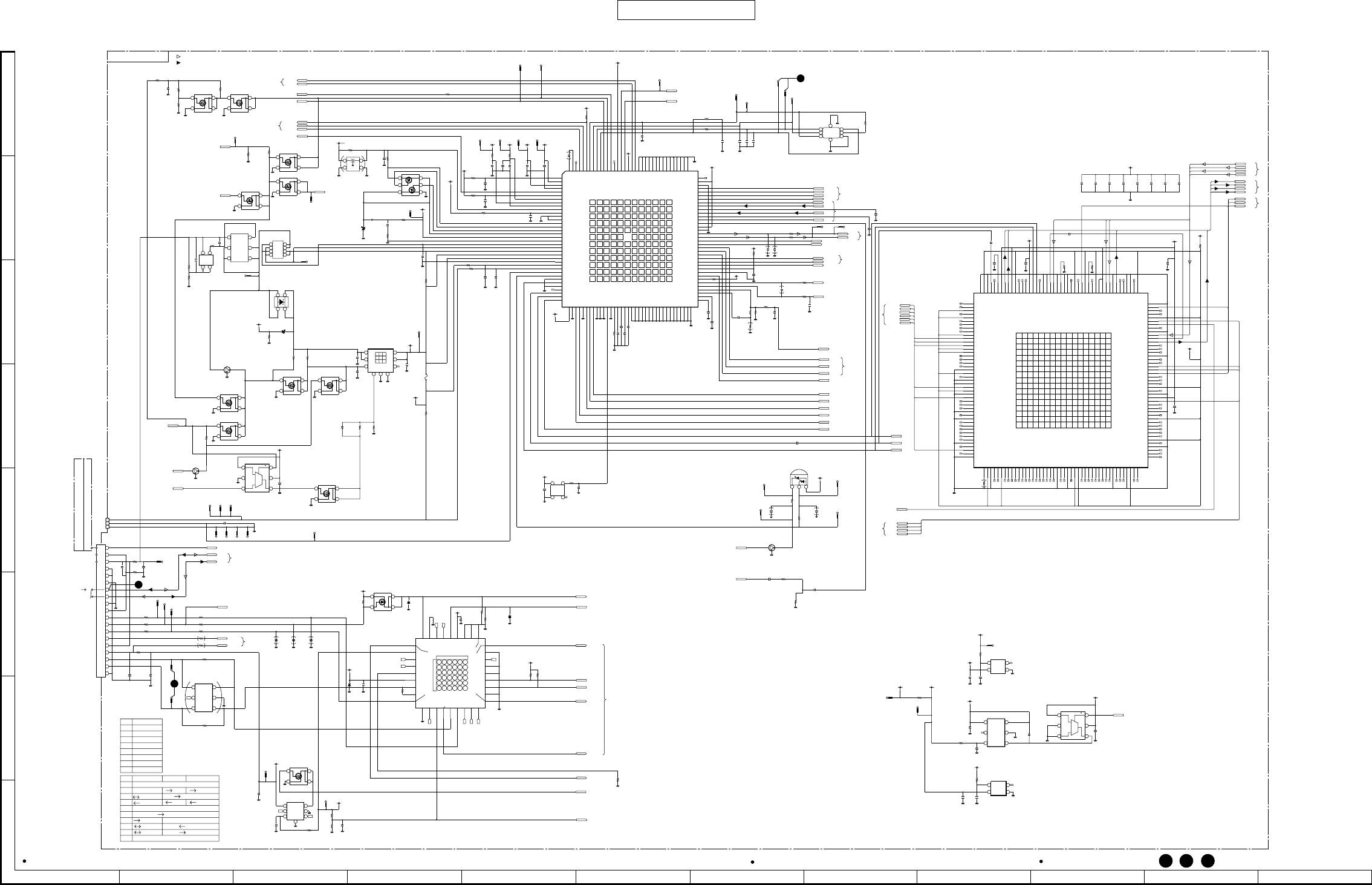
CONFIDENTIAL
5
--
9 5
--
10
Figure 2 SCHEMATIC DIAGRAM (2/9)
902SH 902SH
A
B
C
D
E
F
G
H
12345 6789
10 11 12
NOTES ON SCHEMATIC DIAGRAM can be found on page 5-1. ( ) : Not Mount Waveform numbers of
22
,
32
,
36
are shown on pages 5-3 to 5-5.
MAIN PWB-A(2/6)
SERVICE_N
NS
NDNG
ND
1
23
4
PRGDET
NS
NDNG
ND
1
23
4
NS
NDNG
ND
1
23
4
JACKPOWEN
68
25
A
65
B
12
26
C
9
D
19
62
61
E
48
2
F
42
111
J104
31
106
85
H
140
20
K
141
112
L
69
98
59
78
7
35
70
117
54
142
122
1514
63
143
89
134
27
66
132 139
96
83
G
12
76
16
13
94
107
M
74
60
90
47
87
38
53
17 18
73
43
23
1
4
127
8
5
88
6
81
7
100
44
79
8
113
50
9
130
30
126124
33
109
40
99
128
136
23
45
131
49
37
102
28
138
91
24
133
92
97
135
1
125
29
114
36
64 67
84
6
82
39
105
86
58
115 119
120
22
93
41
4
121
101
77
51
1110
118
116
52 57
21
56
103
123 129
32
110
80
11
108
75
34
10
71
55
3
72
46
5
137
95
SWBUCK
VDDBUCK
VBAT_C
P_BUCK
N_BUCK
LED1
ONSWC
TXON
RESETB
DACCLK
VDD_B
VBAT_A
VSSBUCK
VBUCK
MOD1
DACO1
LED2
INTLCKB
RWRRST
SCL
DACSTR
BDATA
VDD_A
IRQ
SIMOFF
VDD_IO
ONSWA
ONSWB
VSS_C
ADSTR
SDA
DACDAT
EXTLDO
VDDBUF
FGSENSE-
CHSENSE-
VSSTH18
IOUT
VBAT_D
VSSTH 5
PASENSE-
VSSTH15
FGSENSE+
CHREG
VSSTH17
PAREG
VSSTH 4
VSSPA
VSSTH30
VSSTH16
SUB
VSSTH31
VSSTH20
VSSTH21
TEST
GPA13
VSS_D
VSSTH 7
SIMVCC
VSSTH 8
CHSENSE+
VSSTH19
DCIO
VSSTH 6
PASENSE+
VSSTH 1
SIMRST
GPA6
VSSTH26
IREF
DACO3
VSSTH12
SDAT
VSSTH 9
VSS_B
VREF
VSSTH25
PCMI
VSSTH11
SRST
VSSTH22
VSSTH29
VSSTH24
SCLK
VSSTH10
SIMDAT
VSSTH14
GPA12
AUXO2
VSSTH23
VSSTH28
DACO2
VSSTH 3
SIMCLK
GPA7
VSSTH27
VSS_A
VSSTH13
VDDPA
VSSTH 2
PCMCLK
VSSCODEC
BEARN
GPA1
VDDBEAR
MCLK
AUXO1
XTAL2
GPA2
VDD_D
VDD_E
DEC0
AUXI2
VDDLP
CCO
MIC2P
GPA4
AUXI1
MIC1P
GPA3
MIC2N
GPA5
XTAL1
BEARP
VBAT_B
PCMO
PCMSYN
DEC2
MIC1N
VSSBEAR
DEC1
32KHZ
GPA0
46
47
48
49
50
51
52
53
54
55
56
57
58
59
60
61
62
63
CDCDCA
CDCDCB 62
63
6465
41
40
66
67
68
69
70
71
72
73
74
7576
77
78
79
80
81
FF_IN
EXPOUT
82
83
84
85
86
8788
89
90
91
92
93
94
95
96
97
98
99
100
101
102
103
104
105
106
107
108
109
110
111
112
113
114
115
116
117
118
119
120
121
122
123
124
125
126
127
128
129
130
131
132
133
134
135
136
137
138
139
140
VSSADC
VDDADC
141
142
143
29
36
45
37
30
33
26
34
SLEEP
CLK_REQ
110
34
39
43
41
28
35
38
44
32
25
27
31
42
40
18
3
8
9
6
7
15
VIBR
VDDCODEC 136
15
10
14
21
23
24
22
19
13
5
1
2
20
11
17
16
12
4
VBATIB
VCORE15
1
23
4
MIC2P
VANA15
VDIG275
GND
NC
VOUTVIN
1
2
34
VDIG275
NC
VDDB
EXTLDO
VDIG275
VBATI
VDIG275
ONSWC
CCO
VDIG275
WPAREF
VSRAM18
NC
PASENSE
VDIG275
WDCDCREF
1
2
3
45
6
7
8
VMEM18
AUXI1
CHGBYPASS_N
AUXO1
VAPC
PCMCLK
PCMDATB
MIC1P
NC
1
2
3
AUXO2
BEARP
VBATIB
SIMRST0_N
BEARN
PCMDATA
M_I2CCLK
SIMDAT0
PWRRST_N
NS
NDNG
ND
1
23
4
NS
NDNG
ND
1
23
4
NS
NDNG
ND
1
23
4
NS
NDNG
ND
1
23
4
1
23
4
IRQ0_N
PCMSYN
NC
VSRAM18
VDIG275
SIMCLK0
NC
NS
NDNG
ND
NC
ONSWA_N
VCORE15
VBATIB
ND
PG NG
PS PD
NS 1
2
3
4
5
6
M_I2CDAT
VDDA
VBATIB
VCXOCONT
DACSTR
CLKREQ
DACDAT
RTCCLK
ADCSTR
DACCLK
MCLK
VLOOP
PWRREQ_N
RTEMP
TXON
WPOWERSENSE
WRFLOOP
VRTC15
1
23
4NC
NC
HSSLRXCLK
NC
NC
NC
NC
NC
NC
NC
NC
NC
NC
NC
NC
NC
NC
NC
NC
NC
NC
NC
ABCDEFGHJ KLMNPRTU
1
2
3
4
5
6
7
8
9
10
11
12
13
14
15
16
17
1
2
3
6
5
4
7
8
9
10
11
13
12
14
17
16
15
18
19
20
21
22
23
24
25
28
27
26
29
30
31
32
33
34
35
36
37
38
39
40
41
42
43
44
45
46
48
49
47
50
51
52
53
54
55
56
57
58
62
59
60
61
63
64
65
66
67
68
69
70
71
72
73
74
75
76
77
79
80
78
82
83
81
84
85
86
88
87
89
90
91
92
93
94
95
97
96
98
99
100
101
102
103
104
105
106
107
108
109
110
111
112
113
114
115
116
117
118
119
120
121
122
123
124
125
126
127
128
129
130
131
132
133
134
135
136
137
138
139
140
141
142
143
144
145
146
147
148
149
150
151
152
153
154
155
156
157
158
159
160
161
162
163
164
165
166
179
180
178
167
168
169
170
171
172
173
174
175
176
177
(EMIF_A[21])
(EMIF_A[20])
VDD
(EMIF_A[14])
VDD
(EMIF_A[10])
(EMIF_A[9])
(EMIF_A[2])
(CS_BYPASS)
VDD
IS_SYNC_N
HSSLTX_D
HSSLTX_CLK
VDD
VDD
(EMIF_A[23])
(EMIF_A[19])
(EMIF_A[17])
(EMIF_A[12])
VSS
VDD
(EMIF_A[4])
VSS
VSS
IS_EVENT_N
VDD
VSS
HSSLRX_D
(BOOTMODE[1])
(EMIF_D[1])
(EMIF_D[0])
VSS
(EMIF_A[18])
VSS
(EMIF_A[15])
(EMIF_A[11])
(EMIF_A[7])
(EMIF_A[5])
(EMIF_A[3])
(APLL_BYPASS)
VSS
UART_RX
(BOOTMODE[0])
VDD
VSS
IDBALL
(TESTMODE)
VDD
(EMIF_A[22])
(EMIF_D[5])
(EMIF_D[3])
(EMIF_A[16])
(EMIF_A[13])
(EMIF_A[8])
(EMIF_A[6])
(EMIF_A[1])
(ANALOG_ENABLE)
UART_TX
(EMU1)
(EXT_FRAME_STROBE)
VDD
VSS
(EMIF_D[7])
(EMIF_D[6])
(EMIF_D[2])
EMU0
VSS
(JTAG_TDI)
VDD
(EMIF_D[9])
(EMIF_D[8])
(EMIF_D[4])
(JTAG_TDO)
(JTAG_TMS)
(JTAG_TRSTN)
(JTAG_TCK)
(EMIF_D[11])
(EMIF_D[12])
VSS
(GPO[7])
(GPO[6])
VSS
VDD
(EMIF_D[10])
(BOOTMODE[2])
(EMIF_D[15])
(GPO[4])
VSS
(EMIF_D[18])
VDD
(EMIF_D[16])
(EMIF_D[17])
(GPO[5])
(GPO[1])
(GPO[2])
(GPO[3])
VDD
(EMIF_D[19])
VSS
(EMIF_D[20])
(EMIF_D[22])
DAC_DAT
VSS
VDD_DPLL
(GPO[0])
VDD
(EMIF_D[21])
(EMIF_D[24])
(EMIF_D[25])
RADIO_STR
AD_STR
DAC_STR
(CPU_CLKOU)
(EMIF_D[23])
VSS
(EMIF_D[30])
(CPU_IACK)
(CPU_IRQ[1])
DAC_I_OUT
ADC_I_IN_INV
ADC_RXEXTREF_N
VSSA_CS_APLL
(EXT_MEM_UBUS[10])
RESET_N
DAC_CLK
VDD
(EMIF_D[26])
(EMIF_D[27])
VSS
(EMIN_AREADY)
VSS
DAC_Q_OUT
VDDA_BG
VDD
VSS
VDDA_RX
VDD_CLK32
VSS-COMPLEXIO
ADC_Q_IN_INV
DAC_I_OUT_INV
(EMIF_D[29])
CLKRQ
(EXT_MEM_UBUS[12])
(EMIF_AWE_N)
ADC_RXEXTREF_P
VDD
VSSA_BG
VSS-COMPLEXIO
(CPU_XF)
DAC_TXEXTRES
BG_REF
DAC_Q_OUT_INV
CLK32
MCLK
VDD
(EMIF_ARE_N)
VSSA_RX
RADIO_CLK
HCLK
(EMIF_D[28])
ADC_Q_IN
VDD
(EMIF_D[31])
VDDA_CS_APLL
VDD
(CPU_IRQ[0])
VSSA_TX
VDDA_TX
VSS
(EXT_MEM_UBUS[11])
APLL_ATEST1
VSS
ADC_I_IN
VDD
VSS
181
46
47
48
49
50
51
52
53
54
55
56
57
58
59
60
61
62
63
64
65
66
67
68
69
70
71
72
73
74
75
76
77
78
79
80
81
82
83
84
85
86
87
88
89
90
(EMIF_D[13])
(EMIF_D[14])
89
90
91
92
93
94
95
96
97
98
99
100
101
102
103
104
105
106
107
108
109
110
111
112
113
114
115
116
117
118
119
120
121
122
123
124
125
126
127
128
129
130
131
132
133
134
RADIO_DAT 134
135
136
137
138
139
140
141
142
143
144
145
146
147
148
149
150
151
152
153
154
155
156
157
158
159
160
161
162
163
164
165
166
167
168
169
170
171
172
173
174
175
176
177
178
179
180
5
29
36
22
45
24
23
37
17
30
7
12
33
9
1
26
34
39
6
19
43
18
15
13
41
16
21
4
28
35
38
44
HSSLRX_CLK
(BOOTMODE[3])
VSS
45
43
44
3
20
32
25
27
2
8
31
42
40
14
11
10
181
NC
NC
NC
ADCSTR
DACDAT
NC
RESOUT1_N
VANA15
NC
NC
RXIB
WCLK
ISEVENT
RXQB
NC
NC
TXIA
TXQA
NC
HSSLTXCLK
NC
NC
NC
NC
NC
NC
NC
HSSLTX
NC
NC
NC
TXQB
NC
VCORE15_W
NC
NC
NC
NC
NC
NC
NC
NC
NC
NC
NC
NC
NC
NC
NC
NC
NC
NC
NC
NC
NC
NC
NC
NC
NC
NC
NC
NC
NC
NC
NC
NC
NC
NC
NC
NC
NC
NC
NC
NC
NC
NC
NC
NC
NC
NC
DACCLK
DACSTR
NC
WSTR
RXQA
HSSLRX
WDAT
RXIA
NC
NC
NC
VCORE15_W
NC
NC
VRTC15
TXIB
NC
VCORE15
ISSYNC
CHG_C_CNT
USBCHGEN
NC
VDIG275
USBDM
RESOUT0_N
UART1RTS
UART1TX
1
2
3
4
5
6
NC
VBATIB
UART_RXD1
SCLK
BSYNC
BCNT
UART_TXD1
UART_RXD2
654
A
B
D
C
F
E
654123
123
911107128
151413 181716
22 2420 21 2319
25 2926 27 28 30
31 3532 33 34 36
UART_CTS
BDATA
UART_RTS
UART_TXD2
BSSEL
GND
VBAT
PUEA
NC
NC
UARTSEL
UARTMD
CPU_USB_D+
REG33
NC
NC
HEMD
CPUVDD
USBD+/RXD
PU15 BSYNC\SCLK/RTS
GND
RXANAIN
USBMD
CPU_USB_D-
USBD-/TXD
BDATA/CTS
TXANAIN
RXANAOUT
TXANAOUT
1
2
3
4
5
6
7
8
9
10
11
12
13
14
15
16
17
18
19
20
21
22
23
24
25
26
27
28
29
30
31
32
33
34
35
36
USBSENSE
NS
NDNG
ND
1
23
4
UART1CTS
PS
PD
PG
PD
1
23
4
VDIG275
NC
VUSB33
NC
NC
CE
VOUT
VIN
VSS
VSS
NC
NC
1
2
34
5
6
7
VBUS
USBPUEN
NC
USBDP
NC
VDIG275
UART1RX
UARTSENSE
1
2
34
5
6
1
2
3
4
5
6
NC
AUXO1_YMU
FMICLED
VBATI
NC
VDIG275
N.C.GND
VoV+
1
2
3
4
VBUS
NC
1
2
3
4
5
6
7
8
9
ABC
1
2
3
VCC
PE
CONT
GND CMACL
VFB
VOUT
VOUT
1
2
3
456
7
8
9
BU2_ANT
GREEN
RED
23
1
VBATIB
1
2
3
4
5
6
7
8
9
10
11
12
13
14
15
16
17
18
19
RF_IO
ANT_IO
VCCR
TP1200
TP1201
TP1202
TP1203
TP1204
TP1205
TP1206
TP1207
TP1211
TP1217
TP1218
TP1219
TP1220
TP1221
TP1222
TP1223
TP1227
TP1301
TP1302
TP1304
TP1303
TP1305
TP1306
TP1307
1
2
34
TP1229
TP1230
TP1228
TP1231 TP1232 TP1233 TP1234
TP1235
TP1209
TP1210
TP1212
GNDGND
1
2
3
4
TP1213
NC
TP1216 TP1215
PWRREQ_N
1
2
34
5
6
VDIG275
TP1236
TP1237
TP1225
TP1226
VDIG275
M_I2CCLK
M_I2CDAT
SYSCLK0
Power
RESET
CLK I/O
GND
OP
1
2
3
4
5
6
7
8
NS
NDNG
ND
1
23
4
NS
NDNG
ND
1
23
4
NC
SIMRST_N
MIC2N
MIC1N
DACCLK
WRFLOOP
DACSTR
TXON
DACDAT
VLOOP
WPOWERSENSE
SIM_OP
WCLK
DACSTR
ADCSTR
TXIA
TXIB
RXQB
TXQA
RXIA
RXQA
DACCLK
TXQB
RXIB
WDAT
WSTR
HSSLRXCLK
HSSLRX
HSSLTX
SIMDAT
SIMCLK
USBDP
RTCCLK
AUXI2
2MCAMTEMP
SIMVC C
SIMVCC
SIM_IOSIM_CLK
SIM_RESET
VDCIO
VCHG
LEDG
ONSWB_N
VSS
G1
VIN
S2
NC
D2
D2
D1
S1 D1
G2
VOUT
VOUT
VIN VSS
NC
DYIN
DXIN
DXOUT
VBUS
DYOUT
GND
VOUT ECO
VDD
GND
CE
NC
D
G
D
S
D
D
1
23
RFOUT
CHARGER
(-)
CHARGER
(+)
AA/B
BY
GND VCC
Y
TP1308
VBATIB
NC
NC
NC
1
2
34
5
6
AA/B
BY
GND VCC
Y
32
22
36
1
23
1
23
BLUETOOTH AERIAL PWB-K
5-8 (12-E)
5-9 (3-F)
5-17 (6-C)
5-8 (12-E)
5-8 (8-G)
5-8 (9-E)
5-15 (3-H)
5-14 (8-G)
5-8 (12-C)
5-8 (10-A)
5-8 (9-F)
5-12 (8-E)
5-17 (2-G)
5-8 (12-D)
5-8 (10-B)
5-9 (9-F)
5-8 (9-E~F)
5-8 (12-C)
5-8 (12-C)
5-12 (11-D)
5-14 (9-C~D)
5-13 (5-E)
5-14 (7-F)
5-8 (9-E)
5-8 (9-F)
5-8 (12-D)
5-8 (9-F)
5-8 (12-E)
5-9 (3-A)
5-17 (6-C)
5-8 (10-A)
5-14 (8-G)
5-15 (4-A)
5-16 (8-A)
5-15 (2-A)
5-15 (2-A)
5-15 (6-H)
5-15 (2-A)
5-15 (5-H)
5-16 (9-H)
5-16 (9-H)
5-16 (10-H)
5-11 (1-D)
5-15 (5-A)
5-15 (5-H)
5-16 (10-A)
5-8 (12-D)
5-8 (12-E)
5-8 (12-E), 5-15 (3-A)
5-16 (9-A)
5-8 (12-D),
5-10 (8-E)
5-8 (12-D),
5-10 (8-E)
5-8 (9-F~G)
5-8 (12-D),
5-10 (8-D)
5-8 (12-D)
5-8 (12-D),
5-10 (8-D)
5-13 (2-D)
5-13 (3-E)
Synchronisation
TXD
(ANALOG)
GND
RXD
14
Charger (+)
1
Manufacturer
16
3
RF Signal
Reserved
NC
10
CTS
6
18
RF CableDetect
13
Manufacturer
Reserved
GND
USB D-
USB D+
Hands Free
Charger (-)
TX VOICE
Specific
12
(ANALOG)
4
GND
Clock
17
UART
8
NC
7
GND
RTS
USB VBUS
Specific
Power Supply
RX VOICE
11
5
2
GND
9
USB
GND(ANALOG)
Not Defined
15
19 Bluetooth ANT
RECEPTION SIGNAL
TRANSMISSION SIGNAL
5-15 (3-H)
5-16 (9-G)
5-8 (12-D),
5-10 (10-G)
Q1205
EC4401 C
Q1204
EC4401 C
R1205
100K
Q1202
EC4401 C
R1207
1M
IC1200
TWL93004CZQW
POWER SUPPLY/
RF CONTROL
C1203
1
IC1205
S-817A15APF
POWER SUPPLY
C1215
4.7
C1201
0.001
IC1201
XC61CC2002NR
VOLTAGE
DETECTOR
R1237
0
R1215
1
L1201
22µH R1224
0
R1255
0
R1213
15K
R1219
24m
(1/3W)
R1216
0
Q1200
ECH8603
C1204
10
C1214
4.7
C1205
10
C1208
1
C1249
0.1
C1235
0.0012
CN1200
BATTERY
TERMINAL
R1227
100K
R1239
0
Q1207
EC4401 C
R1225
0
R1226
10K
R1214
0.22
C1216
4.7
C1238
100P(CH)
R1234
0
Q1201
EC4401 C
C1229
180P(CH)
C1212
2.2
Q1210
SI1555 DL
C1206
4.7
C1217
1
C1251
1
C1232
0.068
D1201
RB521S30
R1218
0.1
C1236
330P
C1227
1C1228
0.001
C1230
18P(CH)
C1231
18P(CH)
R1230
15K
C1250
1IC1204
S-817A15APF
POWER SUPPLY
C1245
0.1
R1403
0
R1402
100K
C1409
330P
C1406
0.1
C1408
0.1
R1401
43K
C1410
0.1
C1404
0.1
C1412
0.1
C1400
0.1
C1405
0.1
C1411
0.1
C1407
0.1
C1403
0.1
C1402
0.1
C1401
0.1
R1220
0
R1221
0
C1209
1
C1210
1
R1241
0
R1242
0
R1245
0
R1246
0
R1235
1K R1238
1K
C1223
0.1
C1222
0.1
C1221
0.1
C1220
0.1
R1222
0
R1223
0
Q1208
EC4401 C
R1304A
0
R1309
270K
C1307
0.1
IC1300
BU7880GU
EXTERNAL
INTERFACE
Q1300
EC4401 C
R1308
120K
R1307
22K
Q1301
EC4301 C
R1303A
0
R1302A
0
R1310
1.5K
IC1303
XC6219C332DR
3.3 V REGULATOR
R1301
100
R1306A
0
R1300A
0
C1301
0.0056
R1301A
0
C1300
0.0056
R1303
22
R1304
22
R1300
100
R1302
100
R1315
1M
R1316
1M
IC1206
R1163D181B
1.8 V REGULATOR
R1229
0
Q1212
SCH1302
R1217
0
FS1200
2A
C1255
0.1
R1256
56K
R1258
5.6K
C1253
0.1
Q1209
EC4401 C
Q1213
EC4401 C
R1210
100K
R1206
10K
R1203
100K
R1305
0
Q1203
DTC114 YM
C1207
0.1
C1202
0.1
R1208
0
C1211
47P(CH)
C1213
47P(CH)
C1240
0.1
IC1202
TK73840BDB
REGULATOR
LED1200
BRPY121F
SMALL LIGHT
CN1300
EXTERNAL
CONNECTOR
C1241
0.01
R1200
10K
R1201
22K
R1261
100K
C1200
0.01
270
R1244
R1312
1M
R1317
1M
D1202
SB0503EJ
R1211
0
R1266
0
D1200
CUS02Z
C1413
0.1
C1304
1
C1305
1
R1247
0
C1239
2.2
C1246
1
IC1203
LVC1G97Z
LOGIC
C1244
0.1
R1212
2.2K
C1247
1
R1209
22K
R1248
100
R1240
1K
C1414
0.1
IC1401
LVC1G97Z
LOGIC
C1218
4.7
CN1201
USIM CARD
CONNECTOR
C1252
330P
C1226
560P
C1225
560P
C1224
1
R1232
330
Q1214
EC4404 C
Q1215
EC4404 C
R1262
220K
C1260
1
R1264
3.3M
R1263
2.2M
R1265
1M
V1311
100P
C1415
0.1
V1416
650P
R1306
0
D1203
1SS389F
C1303
0.1
C1302
0.1 C1306
1
IC1400
D751980CZPH
W-CDMA MODEM
Q1206
DTC123 EM
IC1209
LM20SITLX
TEMPERATURE SENSOR
C1258
0.1
C1259
0.1
R1260
470
Q1211
DTC114 YM
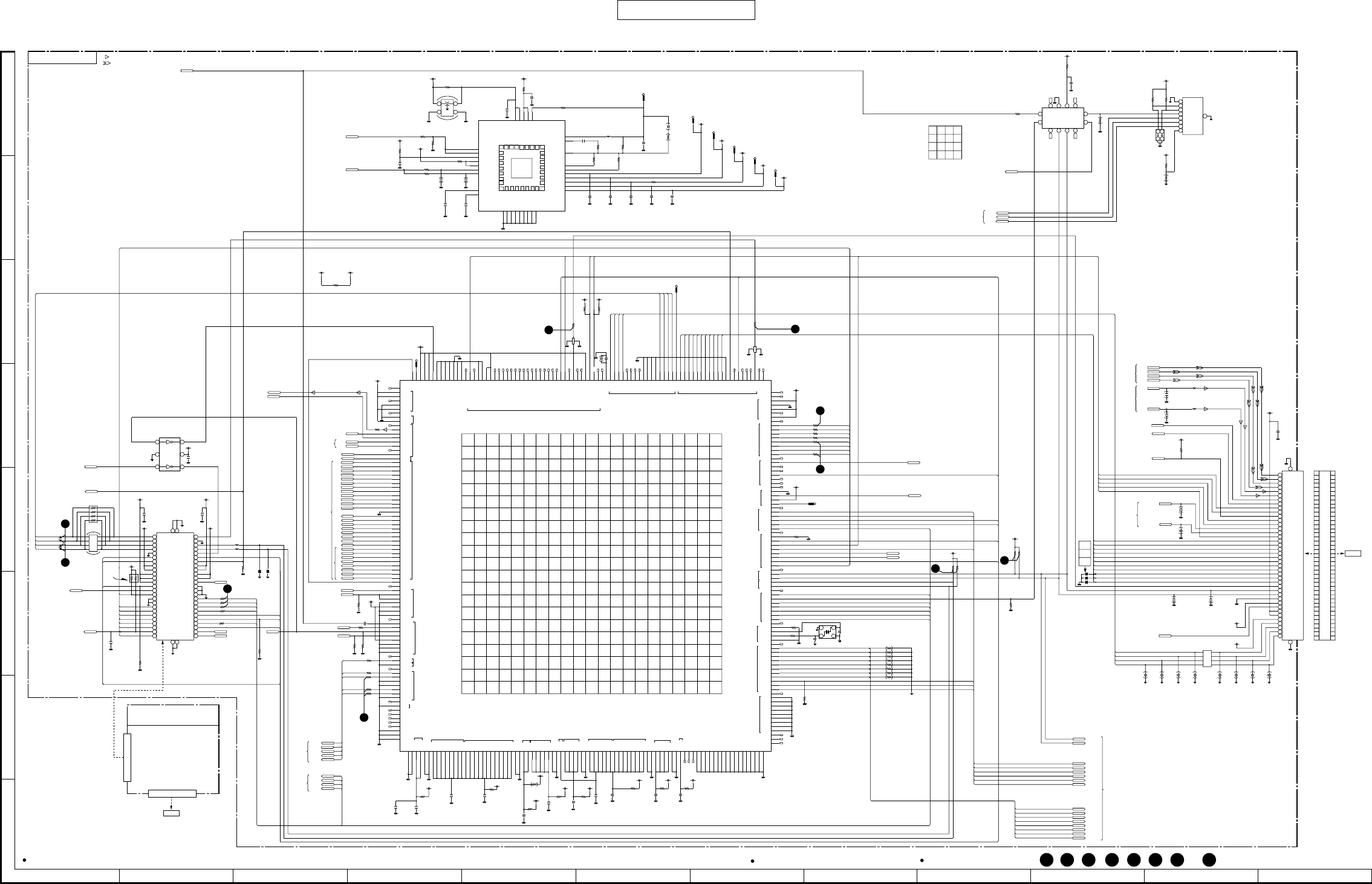
CONFIDENTIAL
5
--
11 5
--
12
Figure 3 SCHEMATIC DIAGRAM (3/9)
902SH 902SH
A
B
C
D
E
F
G
H
12345 6789
10 11 12
NOTES ON SCHEMATIC DIAGRAM can be found on page 5-1. ( ) : Not Mount Waveform numbers of
26
to,
27
,
454329
,
30
,
34
,,
35
are shown on pages 5-2 to 5-5.
MAIN PWB-A(3/6)
26
45
44
43
30
27
29
34
29
35
TO
SD PWB-C
5-23 (3-H)
CN2000
RECEPTION SIGNAL
SPEAKER SIGNAL
VDIG29_T
VDIG29_T
VDIG29_T
VTLVDS25
12
3
4
VTRAM25
VDIG29
VMEM18
VANA15
VTLVDS15
VTRAM15
VDIG29_T
VBATIB VDIG29
BLED+
BLED-
BLED-
BLED+
SP-L1
SP-L2
SP-R1
SP-R2
BEARP
BEARN
FLIP_R
VBATIB
D9
D13
D10
D11
D12
D15
D14
D2
D1
D7
D5
D4
D0
D8
D6
D3
VTLVDS15
VDIG29_T
M_LCD_I2CCLK
M_LCD_I2CDAT
A1
A2
A3
A4
A7
A8
A5
A6
A19
A20
A9
A10
T4G_MEMADV_N
T_I2CDATA
T_I2CCLKA
T4G_PLLLD_N
T4G_STB
T4G_HINT
HCS1_N
LPMODE_N
NC
12
3
4
VDIG275
IRRX
NC
NC
SCL
SDA
VDD
GND
NIRQ
DOUT
NRST
CLKI
NC NC
NC
NC
1234
5
6
7
8
9
10
11
12
IRTX
IRRIRQ_N
GND
TXD-RC
VCC
VIO
SD
RXD
SGND
TXD
LEDA
1
2
3
4
5
6
7
8
9
SYSCLK1
IRCTRL
VDIG29
NC
VBATIB
DISPPXL4
DISPPXL6
DISPPXL3
DISPPXL7
DISPPXL2
DISPPXL1
DISPPXL5
DISPPXL0
NTSC_RST
VAMP_PD
NTSC_PD
BECLK
SEDO
SECLK
AKCS
AMCLK
ADSDI
ADSDO
LRCK
BICK
Y_RESOUT0_N
OE_N
WE_N
NC
NC
NC
NC
NC
NC
NC
NC
NC
NC
NC
NC
NC
NC
NC
NC
NC
NC
NC
NC
NC
NC
NC
NC
NC
NC
NC
NC
NC
NC
NC
NC
NC
NC
NC
NC
NC
NC
NC
NC
NC
NC
NC
NC
NC
NC
NC
NC
NC
NC
NC
NC
NC
NC
NC
NC
NC
NC
NC
NC
NC
NC
NC
NC
NC
NC
NC
NC
NC
VDIG29
HPMUTE_N
AKPD_N
CAMINT
1
2
3
4
5
6
7
8
9
10
11
12
13
14
15
16
17
18
19
20
21
22
23
24
25
26
27
28
29
30
31
32
33
34
35
36
37
38
39
40
41
42
VTRAM25
VTRAM15
VDIG29
VTLVDS25
VTLVDS15
LPMODE_N
T4G_POW VMEM18
VTLVDS15
SDDET_N
LPMODE_N
VMEM18
VBATIB
VDIG29_TVDIG29
VDIG29
TXON
1
2
3
4
1
2
3
4
SP-L1
SP-L2
VCCR
VDIG29
T4G_POW
T4G_STB
CHG_C_CNT
T4G_PLLEN
TP1400
NC
T4G_HDREQ
VBATIB
VDIG29
1
2
34
FB
IN-
CS
ISNS
GND1
LPM
EN1
EN2
EN3
EN4
EN5
GND2
SNSG
VOUT1
VOUT2
VOUT3
VOUT4
VOUT5
VIN1
VIN2
VIN3
GND3
PGND
VOUT
PVCC
VCC
MODE
CREF
GND
GND
GND
GND
GND
1234567
8
9
10
11
12
13
14
15
161718
19
2021
22
23
24
25
26
27
28
29 30
31
32
33 1
2
3
4
5
6
7
8
9
10
11
12
13
14
15
16
17
18
19
20
21
22
23
24
25
26
27
28
29
30
31
32
33
TP1500
TP1501
TP1502
TP1503
TP1504
TP1505
BEHSYNC
BEVSYNC
TP1506
CSYMU_N
1
2
3
456
VDIG29_T
GND
GND
1
2
3
4
VBATIB
1
2
3
45
6
7
8
1
2
3
45
6
7
8
1
2
3
4
56
7
89
10
11
1213
14
15
16
17
18
19
20
21
2223
24
25
26 27 28 29 30 31 32 33 34 35 36 37 38 39 40 41 42 43 44 45 46 47 48 49 50
51 52
53
54
VBT29
TP1507
NC
VS S
LDAT2
VDDV2R
BEDAT2
TSCLK
DTMB
CDAT1
VSS
VDDIOB
VDD1E
TOP VIEW
LDAT10(ERRCAM2)
VS S
BEDAT1
VDDV1R
CDAT5
TSDAT
CDAT0
VDDIOA
VDDIOA
VDD1E
BEDAT0
PLLSEL1
VDDIOB
VS S
LDAT9
VDDV1T
/LWAIT2
CDAT4
CDAT3
/HDREQ
/DACRST
VDDIOB
VDDIOA
PCRXIEN
VDD1E
/PLLLD
GPIO0
LDAT11(ERRCAM1)
VVMID
CDAT6
PLLBPIN
CDAT2
PCRXIN
/LWAIT1
NWDO
PCRXOUT
VDDIOA
VDDIOC
PLLEN
LDAT13(CAM1START)
CDAT7
/MJTRST
VDD1E
VTX1DP
GPIO1
VRX2CKN
SECLK
/LCS2
ADLRCK
NWINT
VTX2DN
HDAT0
VDDIOC
BDCLK
VSS
/HWAIT
VDD1E
GPIO2
VRX2CKP
SEDO
LCLK1
/LCS1
PCRCLK
NWCLK
VTX2DP
LDAT14(ERRLCD2)
BDDAT0
HADR12
VSS
HADR2
VRX1CKN
VDDIOC
VDD1E
VRX2DN
SELD4
GPIO3
VTX1DN
DACCE
/NWOEN
/LRST2
LDAT15(ERRLCD1)
LCLK2
BDDAT1
VRX1CKP
SDDAT2
VDD2E
HADR1
VRX2DP
SELD3
VDDIOC
GPIO4
DACLD
/NWIEN
/HRD
LDAT16(LCDSTART2)
VSS
BDDAT2
VRX1DN
/LRST1
VDD2E
SELD2
SDDAT3
HADR4
VDDIOC
VSSE
DACSD
/HWR
LDAT5
LDAT17(LCDSTART1)
VSS
BDDAT3
VRX1DP
SELD1
LPRCLK
VDD1D
SDCMD
VSS
HADR3
DACCLK
NWDI
/HCS1
VDDIOC
HDAT12
VSSE
VTX2CKN
BDDAT4
LDAT7
HADR11
GPIO5
VTX1CKP
SEDI
LVSIN
VSS
VDD1D
DIRRX
HDAT1
CCLK1
HDAT11
HADR5
VDD1P
VTX2CKP
VSSE
BDDAT5
SYSCLKEN
I2CDATA
HADR10
GPIO6
VTX1CKN
LDAT12(CAM2START)
HDAT3
VDD1D
ADSDOI
HADR6
BDDAT6
VDD1P
VSSE
VDD2E
I2CCLKA
HADR9
GPIO7
HDAT2
LRS
VDD1D
BDDAT7
ADSCKO
HADR7
/RESET
VDD1P
VSSE
VDD2E
/CRST2
HADR8
MJTDO
ADSDO
CVREF
BECLK
/LRD
VDD1D
ADLRCKO
VSS
VDD1P
VSSE
CINT2
HDAT9
HADR0
HDAT14
CHREF
MJTDI
ADSDI
BEHSYNC
/LWR
HDAT15
VDD1D
HDAT4
VSS
HDAT8
VDDIOD
/HVCS2
VSSE
VDD1C
CDCLK
/CRST1
BEVSYNC
ADSCK
MJTCK
SDCLK
HDAT6
VDD1D
HDAT10
/HVCS1
VDDIOB
VSSE
VSSC
CINT1
BEDAT7
LDAT1
MJTMS
SDPWR
HDAT5
VDD1D
/HINT
VDDIOB
/CCS2
/HCS2
BEDAT6
PLLBP
VSSE
/SDDET
VSSVT
LDAT3
HDAT7
VSS
VDD1D
/CCS1
BEDAT5
VDDIOB
POMCLK
VSSE
VDD1D
SDDAT0
LDAT0
LDAT8
VSSVR
SYSCLK
TSFRM
VS S
CCLK2
BEDAT4
VDDIOB
PIMCLK
SDDAT1
VDD1E
VDD1D
LDAT6
VS S
LDAT4
VSSVT
BEDAT3
/TSEN
HDAT13
DTCLK
VDDIOB
VSS
VDD1E
/PDEN
PLLSEL2
HBWSEL
HWTSEL
/LDISPEN
/STBYA
/STBYB
CONFIG0
CONFIG1
CONFIG2
I2CCLKB
I2CDATB
DTVM
PORCTR
BUSSEL
TESTH0
TESTH1
TESTH2
TESTL0
TESTL1
TESTL2
TESTL3
TESTL4
TESTL5
TESTL6
TESTL7
VDD1C
VDD1D
VDD1P
VSS
VSS
VSS
VSSC
B
C
D
E
F
G
H
J
K
L
M
N
P
R
T
U
V
W
Y
AA
A
156101112131415161718192021
22 23 24 25 26 27 28 29 30 31 32 33 34 35 36 37 38 39 40 41 42
43 44 45 46 47 48 49 50 51 52 53 54 55 56 57
58 59 60 61 62 63 64 65 66 67 68 69 70 71 72 73 74 75 76
77 78 79 80 81 82 83 84 85 86 87 88 89 90 91 92 93 94 95 96 97
98 99 100 101 102 103 104 105 106 107 108 109 110 111 112 113 114 115 116 117 118
119 120 121 122 123 124 125 126 127 128 129 130 131 132
133 134 135 136 137 138 139 140 141 142 143 144
145 146 147 148 149 150 151 152 153 154
155 156 157 158 159 160 161 162 163 164 165 166
167 168 169 170 171 172 173 174 175 176 177 178
179 180 181 182 183 184 185 186 187 188 189 190
191 192 193 194 195 196 197 198 199 200
201 202 203 204 205 206 207 208 209 210 211 212 213
214 215 216 217 218 219 220 221 222 223 224 225 226 227
228 229 230 231 232 233 234 235 236 237 238 239 240 241 242 243 244 245 246 247 248
249 250 251 252 253 254 255 256 257 258 259 260 261 262 263 264 265 266 267 268 269
270 271 272 273 274 275 276 277 278 279 280 281 282 283 284 285 286 287 288
289 290 291 292 293 294 295 296 297 298 299 300 301 302 303
304 305 306 307 308 309 310 311 312 313 314 315 316 317 318 319 320 321 322 323 324
325 326 327 328 329 330 331 332 333 334 335 336 337 338 339 340 341 342 343 344 345
NC
NC
NC
NC
NC
NC
NC
NC
NC
NC
NC
NC
NC
NC
NC
NC
NC
NC
NC
NC
NC
NC
NC
NC
NC
NC
NC
NC
NC
NC
NC
NC
NC
NC
NC
NC
NC
NC
C
LVDS C
B
B
B
B
B
B
B
C
B
B
B
B
B
AC
1.5V
D
1.5V 1.5V 2.5V
1.5V
LVDS2.5V
LVDS1.5V
B
D
D
B
B
B
B(VDDIOB)
A(VDDIOA)
B
B
A
(VDDIOA)
1
2
3
4
5
6
7
8
9
10
11
12
13
14
15
16
17
18
19
20
21
22
23
24
25
26
27
28
29
30
31
32
33
34
35
36
37
38
39
40
41
42
43
44
45
46
47
48
49
50
51
52
53
54
55
56
57
58
59
60
61
62
63
64
65
66
67
68
69
70
71
72
73
74
75
76
77
78
79
80
81
82
83
84
85
86
87
88
89
90
91
92
93
94
95
96
97
98
99
100
101
102
103
104
105
106
107
108
109
110
111
112
113
114
115
116
117
118
119
120
121
122
123
124
125
126
127
128
129
130
131
132
133
134
135
136
137
138
139
140
141
142
143
144
145
146
147
148
149
150
151
152
153
154
155
156
157
158
159
160
161
162
163
164
165
166
167
168
169
170
171
172
173
174
175
176
177
178
179
180
181
182
183
184
185
186
187
188
189
190
191
192
193
194
195
196
197
198
199
200
201
202
203
204
205
206
207
208
209
210
211
212
213
214
215
216
217
218
219
220
221
222
223
224
225
226
227
228
229
230
231
232
233
234
235
236
237
238
239
240
241
242
243
244
245
246
247
248
249
250
251
252
253
254
255
256
257
258
259
260
261
262
263
264
265
266
267
268
269
270
271
272
273
274
275
276
277
278
279
280
281
282
283
284
285
286
287
288
289
290
291
292
293
294
295
296
297
298
299
300
301
302
303
304
305
306
307
308
309
310
311
312
313
314
315
316
317
318
319
320
321
322
323
324
325
326
327
328
329
330
331
332
333
334
335
336
337
338
339
340
341
342
343
344
345
VDIG29_T VDIG29_T
VDIG29
1
2
3
45
6
7
8
SDDET_N
SDPWR
SDEN
VRX2DP
VRX2DN
VRX2CKP
VRX2CKN
VTX1DP
VTX1DN
VTX1CKP
VTX1CKN
SLCDCE
SECLK
SEDO
BDRST
BDCE
LEDLD
LEDRST
FLOW
RSTGA
BLED+
LCDRST
VDON
CDAT0
CDAT1
CDAT2
CDAT3
CDAT4
CDAT5
CDAT6
CDAT7
HSYNC
VSYNC
PCCLK
ZMPEN
SDCMD
SDDATA3
SDDATA2
SDDATA1
SDDATA0
SDCLK
CAMCLK
NTSC_RST
VAMP_PD
NTSC_PD
AKCS
LCDINT
AKPD_N
DISPPXL7
DISPPXL6
DISPPXL5
DISPPXL4
DISPPXL3
DISPPXL2
DISPPXL1
DISPPXL0
CDAT7
CDAT2
VSYNC
PCCLK
VTX1DP
VTX1DN
VTX1CKP
VTX1CKN
TXON_N
FLOW
LEDLD
SEDO
SECLK
SLCDCE
SLCDDC
BDCE
SLCDRST
SDEN
SDCLK
SDDATA2
SDDATA3
SDDATA0
SDDATA1
SDCMD
SDPWR
ZMPEN
RSTGA
HSYNC
CDAT1
CDAT0
CDAT3
CDAT4
CDAT6
CDAT5
LCDRST
LCDINT
VDO N
VDWAIT
LVSIN
SLCDRST
SLCDDC
BEHSYNC
BEVSYNC
VRX2DP
VRX2DN
VRX2CKP
VRX2CKN
SDDET_N
AMCLK
ADSDO
ADSDI
BICK
LRCK
BECLK
BDRST
LEDRST
VDWAIT
LVSIN
CAMINT
CAMINT
CAMINT
SYSCLK
POW_ECO
VSYNC
POW_CE
BLED-
VTX1DP
SDA(CAM
LCDINT
D1(CAMPXL0)
VTX1CKN
SP-R1
VCCR
SP-R2
LVSIN
SP-L1
VTX1DN
SCL(CAM
SDA(LCD
VTX1CKP
PCCLK
BATTCAM
HSYNC
BLED+
SUBCAMTEMP
SCL(LCD
EAR
LCDRST
XEAR
VDWAIT
BATTLCD
SP-L2
FLIP_R
VDON
BATTBB
SDCLK
GND
GND
LVDSCKN
BATTBB
VCC
LEDRST
DC_B
BDRST
LVDSDN
FLOW
GND
SDDET
ZMPEN
LEDLD
SEDO
GND
BATTBB
LVDSCKP
RSGA
LVDSDP
SDPWR GND
BATTBB
SLCDRST
I2CCLKB(2MCAM)
SDDATA0
BATTBB
BDCE
GND
SDEN
SDDATA3
SCEB
I2CDATB(2MCAM)
EXCKI
SDDATA1
VCC
VCC
SDDATA2
SECLK
VCC
TXON_N
GAINT
SDCMD
BLED+
BLED-
GND
D0(CAMPXL0)
D3(CAMPXL0)
D4(CAMPXL0)
D6(CAMPXL0)
D5(CAMPXL0)
D7(CAMPXL0)
D2(CAMPXL0)
3
IC1502
2
6
4
4
A
9
IRDA+IRLED
D
3
11
7
12
10
5-13 (2-D)
5-8 (12-D)
C
5
1
B12
8
SP-
SP+
GND
1A
VCC
2Y2A
1Y
23 4 7 8 9
15610111213141516171819202123 4 7 8 9
COAXIAL
CABLE
TO
DISPLAY
PWB-B
5-21 (2-E)
CN3001
SD P.W.B. CONNECT
FPC PWB-H
5-12 (8-E)
5-7 (3-A)
5-8 (12-B)
5-13 (4-H)
5-13 (2-C)
5-7 (1-A)
5-7 (1-H)
5-13 (2-B),
5-7 (1-F)
5-14 (8-C)
5-10 (8-B)
5-8 (12-C)
5-11 (3-F)
5-13 (5-F~H)
5-11 (1-F)
5-11 (2-F)
5-11 (3-F)
5-9 (2-E)
5-13 (6-F)
5-11 (3-A)
5-8 (10-A)
5-8 (12-C)
5-8 (12-C)
5-7 (1-A~B)
5-13 (2-B)
5-13 (2-D),
5-8 (12-D)
5-12 (8-E)
5-8 (12-B)
5-10 (8-D)
5-8 (10-B)
5-12 (11-D)
5-8 (10-A)
5-12 (11-D)
5-13 (2-C)
5-13 (4-G)
5-8 (10-A)
5-12 (11-F)
5-8 (10-A)
5-8 (10-B)
5-17 (1-A)
R1554
0
R1525
1M
R1534
0
R1546
0
R1509
0
R1526
560
C1521
0.1
R1578
0
C1524
0.1
C1523
100P
(CH)
R1557
0
C1554
15P
(CH)
C1555
15P
(CH)
RA1547
22
C1503
0.1
C1502
0.1
RA1561
100K
R1561
1M
C1587
0.1 CN1500
L1501
600nH
L1500A
600nH
R1507
1M
V1500
33P
V1501
33P
R1502
0
R1503
0
R1504
0
R1505
0
R1506
0
R1562
1M
R1559
1M
R1560
1M
R1564
0
R1563
100
R1565
100
R1572
100
R1571
100
R1508
1M
R1547
100K
C1505
0.0033
R1517
0
R1574
1M
R1575
1M
FL1500
NOISE FILTER
C1513
0.001
R1522
0
FL1501
NOISE FILTER
R1529
47
R1530
47 R1531
47
R1532
47
R1528
47
R1533
100
R1576
0
R1524
100K
R1523
680 C1517
15P
(CH)
C1518
15P
(CH)
X1500
27MHz
R1527
1M
C1516
1
C1515
1
C1514
1
R1520
0
R1519
0
R1511
0
C1512
1
C1511
1
R1518
0
C1509
1
R1516
0
C1510
1
R1515
10
C1508
1
R1514
0
C1507
1
C1506
1
R1512
0
C1504
1
IC1500
TC3525XBG
MULTIMEDIA ACCELERATOR
R1543
1K
R1542
1K
R1551
1M
R1545
3.3K
R1544
3.3K V1552
100P
V1553
100P
V1551
100P
RA1500
100 at 100MHz
C1519
1
CN1501
L1566
600nH
L1567
600nH
R1573
1M
R1549
0
CA1521
1
LED1503
GP2W3240
INFRARED
PORT
R1548
0
R1550
10
C1520
0.1
R1558
0
R1570
0
IC1502
BU7876GL
INFRARED
REMOTE
Tx CONTROLLER
LSI
C1530
10
R1539
82K
C1528
10
C1526
4.7
C1529
4.7
C1531
1
C1532
1
R1541
0
R1556
0
C1527
100P
(CH)
R1537
10K
R1538
0
R1540
120K
L1500
2.2µH
C1525
10
C1542
2.2
R1555
1
IC1504
FA3727R
POWER CONTROL
C1582
0.1
IC1505
LVC2G04Z
LOGIC
R1510
0

CONFIDENTIAL
5
--
13 5
--
14
Figure 4 SCHEMATIC DIAGRAM (4/9)
902SH 902SH
A
B
C
D
E
F
G
H
12345 6789
10 11 12
NOTES ON SCHEMATIC DIAGRAM can be found on page 5-1. ( ) : Not Mount Waveform numbers of
28
,
37
,
48
are shown on pages 5-4, 5-5.
MAIN PWB-A(4/6)
CCO
VDIG275
PS
PD
PG
PD
1
23
4
NS
NDNG
ND
12
3
4
MIC1P
1
2
34
5
VDIG275
VDIG275
AGND
JMIC
JACK
JEARL
MONO+ST
JEARR
VCC(2.9V)
UART-RX
UART-TX
DGND
GND
(for Connecter Body)
(for Connecter Body)
GND
1
2
3
4
5
6
7
8
9
10
11
12
NC
VIB1601
VIB1600
VBATIB
NC
VMEM18
NC
NC
NC
NC
GPIO3
GPIO1
BCLK
D7
D4
D1
D0
NC
MTR
LED1/GPIO4
GPIO2
SDI
/IRQ
D5
D2
IOVDD1
CLKI
GPIO0
DVSS
LED2/GPIO5
D3
LRCK
A0
/WR
D6
RXIN
LED0
DVDD
IOVDD2
DVDD
TXOUT
/CS
EQ2R
SPVDDL
/RST
HPOUTL/MONO
EQ3R
EXTIN
NC
EQ1R
NC
NC
PLLC
EQ2L
NC
EQ1L
EQ3L
NC
HPC
/RD
SPOUT2L
BBL
SPVSSR
HPOUTR
NC
EXC
(SPOUT1R)
SPOUT2R
SPVDDR
VREF
SPOUT1R
SPOUT1L
SPVSSL
BBR
(SPOUT1L)
AVDD
AVSS
NC
EXTOUT
AB DCGHFEJ
9
6
7
8
5
2
3
4
1
9
8
10
11
12
14
15
13
17
18
16
20
21
19
22
23
24
26
27
25
30
28
32
33
31
34
35
29 36
38
39
37
40
41
42
43
45
46
44
47
48
49
51
54
55
53
50
52
59
60
61
57
56
58
64
62
63
66
65
67
70
68
69
72
73
71
7
6
5
4
3
2
1
DVSS
IOVDD2
IOVDD2
1
2
3
4
56
7
8
9
10 11
12
13
14
15
16
17
18
19
20
21
22
23
24
25
26
27
28
29 30 31
32
33 34
35
36
37
38
39
40
41
42
43
44 45 46
47
48
49
50
51
52
53
54
55
56
57 58
59 60
61
62
63
64
65 66
67
68
69 70
71
72 73
NC
VBATIB
VDIG29
NC
NC
NC
NC
VANA29
VDIG29
NC
NC
NC
NC
NC
12
34
SP-L1
SP-L2
SP-R1
SP-R2
MIC2P
AUXI1 MIC200
MIC201
AUXO2
AUXO1
D7
D6
D5
D4
D3
D2
D1
D0
OE_N
WE_N
A1
LRCK
BICK
ADSDO
AMCLK
ADSDI
HIFIDET_N
UART0RX
UART0TX
ONSWPUEN
VAMP_PD
JACKDET_N
PRGDET
JACKPOWEN
SYSCLK1
FMICLED
CSYMU_N
1
2
34
5
6
1
2
34
5
6
VDIG29_T
HPMUTE_N
1
2
3
4
5
NC
12
25
3534
14
20
B
52
4
H
2
48
A
15
41
39
29
43
38
47
6
61
8
8
36
D
30
24
54
28
9
51
1
40
1713
33
2
11
42
7
18
32
19 23
53
7
J57
3
37
4
45
16
G
56
26
E
46
55
5
49
C
5
31
22
10
9
50
21
27
F
44
3
AVSS
DVDD
DVDD
DVSS
AVDD
DVSS
DVDD
AVDD
AVSS
INDEX
DVSS
DVSS
DVDD
AVSS
VREFOUT
NC
SELA
NC
NC
TEST
NC
NC
NC
IREF
SYSINV
TEST
VREFIN
NC
NC
HSYNC
D7
D1
FID/VSYNC
C
D4
D2
D5
D3
Y
CVBS
D6
D0
SYSCLK
/RESET
UD7
UD9
PD
UD4
UD6
UD1
UD8
UD5
SDA
UD3
UD0
SCL
UD2
1
2
3
4
5
67
8
9
10
11
1213
14
15
16
17
18
19
20
21
22
23
24
25
26
27
2829
30
31
32
33
34 35
36
37
38
39
40 41 42
43
44
45
46
47
48
49
50
5152 53
54
55
56
57
CCLK
MIN
LIN
RIN
AVSS
AVDD
VREF
VCOM
MUTET
HVDD
HVSS
HPR
HPL
AINL2
MOUT
AINL1
AINR1
AINR2
CSN
PD N
CDTI
LRCK
MCLK
BICK
DVDD
SDTI
DVSS
SDTO
1
2
3
4
5
6
7
8910 11 12 13 14
15
16
17
18
19
20
21
2223
24
25
26
27
28
NC
DISPPXL7
DISPPXL0
DISPPXL4
DISPPXL2
DISPPXL6
DISPPXL1
DISPPXL3
DISPPXL5
NTSC_PD
NTSC_RST
BECLK
VDIG29
NC
NC
NC
NC
NC
NC
NC
NC
NC
NC
NC
NC
NC
NC
NC
NC
NC
NC
NC
NC
T_I2CCLKA
T_I2CDATA
AKCS
SECLK
SEDO
AKPD_N
VDIG29 VDIG29
VBATIB
PS
VOUT
VSAG
VIN
GND
V+ 1
2
3
4
5
6
AUXO1_YMU
TDO
TCK
TRST_N
TDI
RTCK
TMS
MIC1_BIAS
VDIG29
VDIG29
1
2
34
5
6
VBATIB
VMEM18
LPMODE_N
VANA29
VBATIB
VDIG29
1
2
3
4
56
7
8
910 11 12 13 14 15 16
17 18 19 20 21 22 23 24
2526272829303132
33 34 35 36 37
VBATIB
NC
NC
NC
NC
VANA29
VANA29
YMUINT_N
TP1600
Y_RESOUT0_N
TP1601
TP1602
TP1603
TP1604
TP1605
TP1606
BEHSYNC
BEVSYNC
1
2
3
4
1
2
3
4
MIC_GND
TP1609
NC
NC
NC
NC
1
2
34
5
6
TP1607
TP1608 TP1611
TP1610 TP1612
TP1614
TP1613
VDIG29
TP1800
VDIG275
D0
D1
D2
D3
D4
D5
D6
D7
A1
OE_N
WE_N
VIBREG_CONT
VAMP_PD
AMCLK
ADSDI
ADSDO
LRCK
BICK
LRCK
AMCLK
BICK
LRCK
BICK
ADSDO
HPOUT_L
ADSDO
ADSDI
AGCONOFF
SPSAVE
STBONOFF
STBONOFF
SPSAVE
AGCONOFF
SUROUNDSW
SUROUNDSW
HPOUT_R
AUX1_BIAS
MIC2_BIAS
VCC
NC
GND
CPU-I/F
STBY
GND
Vin
NC
Vout
GND
CE ECO
Vout
VDD
GND
SURROUND
AGC ON/OFF
SP_SAVE
STB ON/OFF
GND
IN-R
IN-L
VCC
Vref
C1
R1
C2
R2
AGCDET
VREFSP
VCC
R-ch L-ch
VCC
C3
R3
VREFSP
SPATIALIZER
AGCAGC
AGC_det
ON/OFF
VIDEO OUT/
HANDSFREE
MICROPHONE
CONNECTOR
CE
ECO
NC
VDD
GND
VOUT
VDIG29
28
48
37
37
MIC200
MICROPHONE
M
5-7 (1-A~B)
5-13 (2-B)
5-7 (1-B)
5-11 (3-D)
5-10 (7-E)
5-11 (3-G)
5-12 (10-G~H)
5-8 (7-F)
5-8 (9-E)
5-8 (7-F)
5-8 (10-A)
5-8 (7-F)
5-8 (10-A)
5-8 (7-F)
5-8 (10-A)
5-9 (2-B)
5-9 (2-A)
5-8 (10-A)
5-10 (8-B)
5-12 (11-D)
5-12 (11-D)
5-8 (8-G)
5-8 (7-G)
5-11 (3-H)
5-10 (8-B)
5-12 (3-E)
5-7 (3-A)
5-8 (12-B)
5-11 (3-B)
5-8 (10-B)
5-10 (7-F)
5-8 (12-D),
5-11 (3-F)
5-11 (2-A),
5-8 (12-D)
5-7 (1-F)
5-11 (3-D)
5-10 (8-B)
RECEPTION SIGNAL
TRANSMISSION SIGNAL
SPEAKER SIGNAL
R1649
2.2K
R1643
3.3M
Q1605
EC4301 C
Q1604
EC4401 C
R1652
0
R1606A
0
IC1604
LVC1G07Z
LOGIC
L1600
FERRITE BEADS
JK1600
C1645
0.1
R1603
0
R1644
1M
L1602
FERRITE BEADS
L1601
FERRITE BEADS
C1718
100/4
C1721
10
C1714
1
R1718
150
C1722
100/4
R1717
150
C1720
10
R1626
15
R1625
15
C1713
4.7
R1638
1K
C1631
0.1
R1619
33K
C1622
0.027
R1610
0
C1612
0.001
R1609
0
R1615
0
R1607
0
R1613
0
IC1600
YMU783C
MOBILE AUDIO
R1611
3.3K
R1602
0
R1617
120K
C1604
4.7
C1621
0.027
R1618
120K
R1620
33K
C1626
120P(CH)
R1614
0
R1616
0
C1613
0.1
R1606
0
C1625
120P(CH)
R1663
0
CA1609
1
C1634
0.1
C1637
4.7
R1639
4.7K
R1648
1K
R1651
2.2K
R1650
1K
C1642
4.7 C1646
4.7
C1644
0.1
C1633
0.1 R1661
0
R1662
0
R1667
100
R1641
3.3M
C1723
0.1
R1716
0
C1614
0.1
R1612
0
Q1601
HN1C03 FUZ
Q1602
EMT1
R1627
1M
IC1601
BH30FB1WHFV
VIBLATOR
REGULATOR
IC1800
AK8813P
NTSC ENCODER
IC1700
AK4569
PCM
CODEC
C1800
4.7
R1802
0
C1802
0.1
R1803
6.8K
C1803
4.7
C1704
0.1
C1705
0.1
C1703
0.1
C1709
4.7
C1706
1
C1702
4.7
C1700
0.1
C1640
1
C1647
1
IC1701
MM1671XN
VIDEO AMP.
R1634
100
R1668
0
R1719
0
R1806
10
R1720
0
C1666
1
C1667
1
R1724
0
R1723
0
R1704
1M
C1671
0.047
C1672
0.047
C1627
1
C1628
1
C1673
4.7
C1675
680P
C1674
680P
R1673
0
IC1603
AN12974A
AGC STEREO AMP.
R1624
0
R1646
0
R1642
0
R1645
0
R1656
0
C1602
0.1
C1678
0.1
C1632
0.1
C1620
0.1
C1680
1
C1676
1
C1610
1
C1600
1
C1648
1
C1624
1
R1621
1M
R1636
1M
R1655
1M
R1635
1M
R1659
10K
R1622
10K
R1657
10K
R1623
10K
R1660
100K
C1677
0.0047
C1601
0.0047
C1605
0.001
C1679
0.001
C1650
0.022
R1653
2.2K
C1629
100/4
C1630
100/4
R1630
3.3K
R1678
3.3K
R1628
100K
R1679
100K
V1602
15P
RA1800
100K
RA1647
560K
C1652
0.1
C1664
0.1
C1665
0.1
C1681
0.47
R1658
0
0.1
C1684
R1666
0
R1804
0
C1682
2.2
D1600
RB521G30
D1601
RB521G30
IC1602
R1163D291B
2.9 V REGULATOR
C1716
0.1
C1717
0.1
C1608
1
C1619
0.1
C1611
0.1
C1623
0.1
C1635
0.1
C1607
0.1
C1603
0.1
C1606
1
C1701
2.2
C1707
1
C1801
1
R1631
0
R1807
3.9K
D1603
RB521G30
R1711
180
L1654
600nH
R1664
10
R1665
10
C1654
0.1
V1653
15P
C1655
0.1
C1651
0.1
VIB001
VIBLATOR
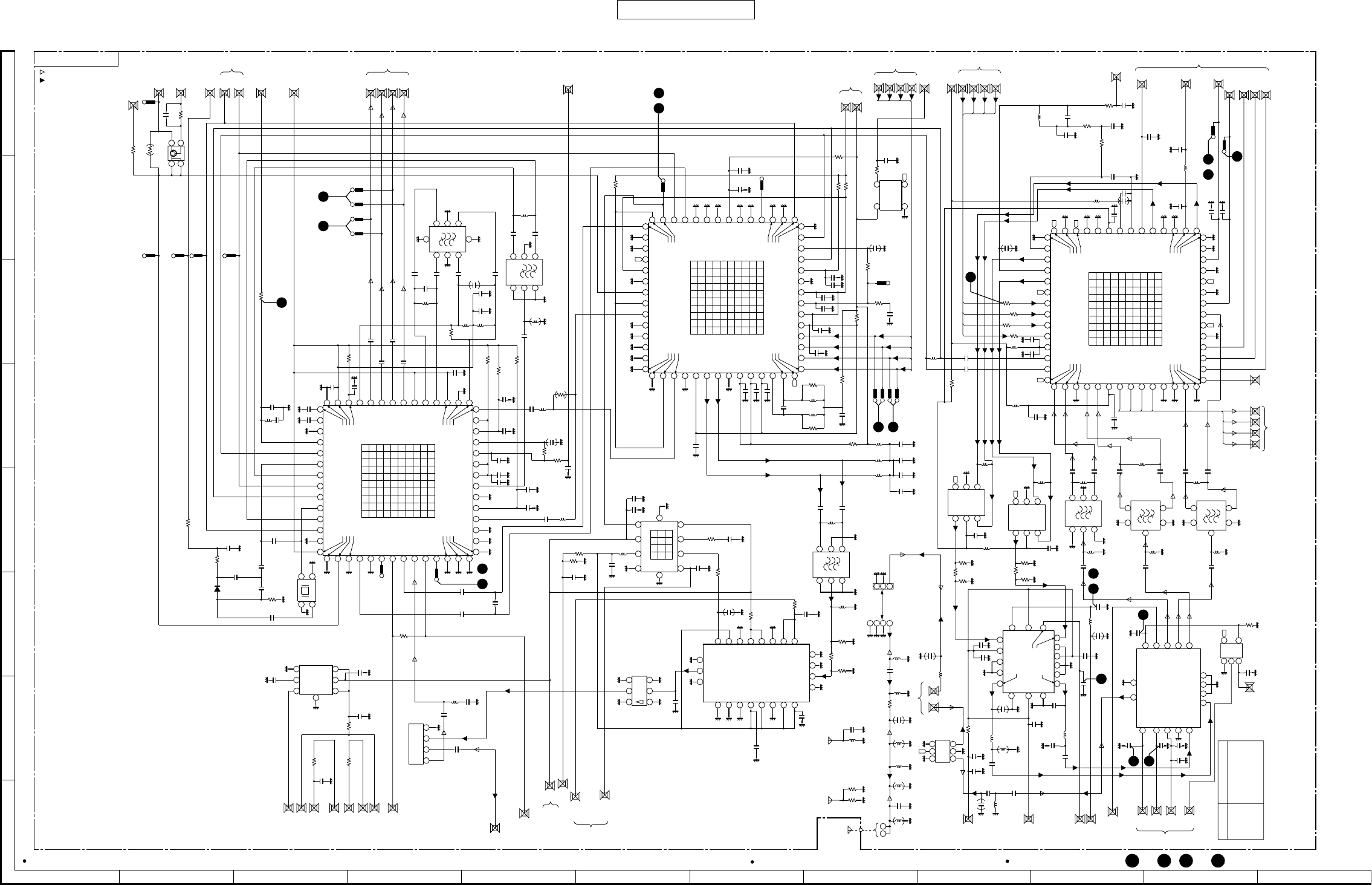
CONFIDENTIAL
5
--
15 5
--
16
Figure 5 SCHEMATIC DIAGRAM (5/9)
902SH 902SH
A
B
C
D
E
F
G
H
12345 6789
10 11 12
NOTES ON SCHEMATIC DIAGRAM can be found on page 5-1. ( ) : Not Mount Waveform numbers of to
2114
to
111
, are shown on pages 5-2, 5-3.
A
B
C
D
E
F
G
H
J
K
11 12
13 14 15 16 17 18 19 20
21 22 23 24
25 26 27 28
29 30 31 32
33 34 35 36
37 38 43 4439 40 41 42
45 46
47 48 49 50 51 52 53 54 55 56
1234567890
1234567890
GNDRF
RFHC
RFHD
NC
RFLB
RFLA
VCCRF
QRB
QRA
IR B
IR A
GNDRF
REON
GNDPLANE
RFHA
GNDVCO
CLK
DATA
STROBE
GNDVCO
NC
RFHB
TXON
GNDVCO
NC
GNDRF
RXON
GNDVCO
GNDSILENT
TXOLB
BSEL
GNDVCO
GNDVCO
TXOLA
PCTL
GNDVAR
VCCVCO
VCCBUF
GNDBUF
NC
PS
GNDPLL
XOOLA
NC
TXOHB
PHDOUT
TXOHA
NC
MODA
MODB
MODC
MODD
VCCPLL
XOOB
XOOC
VTUNE
A
B
C
D
E
F
G
H
J
K
11 12
13 14 15 16 17 18 19 20
21 22 23 24
25 26 27 28
29 30 31 32
33 34 35 36
37 38 43 44
39 40 41 42
45 46
47 48 49 50 51 52 53 54 55 56
12345678910
1234567890
IFINA
IFINB
VCCLF
QRA
QRB
IRA
IRB
IFOUTB
VCCREF
VCCMIX
GNDIF
CDQ
CDI
GNDLF
MCLK
XOOA
XOIA
MIXINA
DATA
XOOB
XOIB
MIXINB
CLK
GNDREF
GNDBUS
STROBE
GNDBIAS
VCCBUS
IFLOA
GNDEME
GLNA
REFON
IFLOB
RFI N
XOOON
GNDPLL
GNDPHD
GNDTUNE
GNDVCO
RXON
GNDRFLO
GNDBYP
RFLOOA
VCCRF
INDBYP
RFOUT
VCCPLL
VCCPHD
PHDOUT
VTUNE
VCCVCO
VCCRFLO
RFLOOB
IFOUTA
GNDMIX
VCCIF
G
RF_CLKREQ
G
WSTR
GVCXOCONT
GWCLK
GWDAT
GMCLK
GRXIB
GRXIA
GRXQB
GRXQA
GWRFLOOP
G
WPOWERSENSE
G
WDCDCREF
G
WPAREF
G
VBATI
G
V_WIVI
G
V_WIVI
G
RTEMP
G
TXIA
G
TXIB
G
TXQA
G
TXQB
G
MODD
G
MODC
G
MODB
G
MODA
G
VCCA
G
BSEL0
G
RADCLK
G
RADDAT
G
RADSTR
GVLOOP
G
PCTL
G
IRA
G
IRB
G
QRA
G
QRB
G
RXON
G
TXON
G
BSEL0
G
VAPC
G
VBATI
G
WCDMA
G
ANTSW2
G
ANTSW1
G
ANTSW0
SP001
SP002
SP003
SP004
G
GPRFCTRL
G
GPRFCTRL
GVCCB
G
EXTLDO
5-9 (3-A)
5-16 (8-A)
5-9 (5-A)
5-9 (5-A)
5-16 (9-A)
5-16 (11-G)
5-15 (3-A)
5-15 (2-A)
5-16 (8-A)
5-8 (12-D)
5-16 (10-H)
5-16 (11-D)
5-10 (8-C)
5-16 (9-H)
5-10 (8-D)
5-10
(8-C)
5-10 (8-C)
5-15 (5-H)
5-10 (8-C)
5-10 (8-C)
5-8 (9-E)
5-15 (5-H)
5-8
(9-F)
MAIN PWB-A(5/6)
G
VDDA
G
VCCA
G
VDDB
G
VCCB
G
V_WIVI
G
V_WIVI
G
PASENSE
SP008
897.50MHz
1,810.00MHz
G
WCDMA
5
6789
4321
4321
10
A
B
C
VREG
VREG
GND
VCCBIAS
VCCBIAS
GND
VCCDET
GND
VDETECT
GND
GND
GND
GND
GND
GND
GND
GND
VCC2
VCC2
VCC1
VCC1
RFIN
RFOUT
SP009
SP015 SP016 SP017 SP018
SP022
SP023
SP019
SP020
SP021
G
VCCB
GVCCB
SP027
G
VCORE15
NCGND
VoV+
DCS_PCS out
GSM_Pout
GSM_Pin
Vcc
Vcc
Vsupply
VAPC
DCS_PCSin
Vcc
BS
GND
GND
GND
GND
GND
GND
GND
DCS1800Rx
GND
GSM1900RX
VC1
GSM900Rx
VC2
ANT
Vdd
GND
VCG
WCDMA
GND
GND
DCS1800Tx
GND
GSM900Tx
A
B
C
D
E
F
G
H
11 12
13 14 15 16 17 18 19 20
21 22 23 24
25 26 27 28
29 30 31 32
33 34 35 36
37 38 43 4439 40 41 42
45 46
47 48 49 50 51 52 53 54 55 56
1234567890
1234567890
I
J
QINBAR
QIN
IINBAR
IIN
VCCBB
VCCIFPHD
PHDIFOUT
VCCIFPLL
GNDIFVCO
VCCIFVCO
XOOB
VTUNEIF
XOOC
GNDBB
CLK
GNDIFPHD
GNDIFPLL
GNDRFVCO
GNDTUIF
VCCBUS
GNDBUS
GNDRFPHD
GNDIFVCO
IFLO
DATA
TXON
VCCRFPHD
GNDIFLO
GNDRFPLL
PHDRFOUT
VCCIFLO
GNDRFLO
STROBE
VCCRFPLL
RFLO
GNDRFLO
GNDRF
GNDRF
GNDRF
GNDIF
GNDRFVCO
GNDTUNERF
VCCRF
OUT
OUTBAR
GNDRF
MIXOUT
MIXOUTBAR
VTUNERF
G
RF_I O
G
ANT_IO
2110-2170MHz
SP028
SP029
DUPLEXER
ANT GNDRX TX
SP031
SP032
NC
WRFLOOP
MODA
MODB
MODC
MODD
IR B
QRA
QRB
QRB
QRA
IRB
IRA
TXQB
TXQA
TXIB
TXIA
XOOB
XOOB
G
ANTSW3
WDAT
WDAT
XOOA
XOOA
XOOA
RF_CLKREQ
WSTR_WOPY_WIV I
WSTR_WOPY_WIVI
WCLK
WCLK
VCXOCONT
IR A
EGSMTx H
CONTROL LOGIC
GSM1900Rx L
EGSMRx L
GSM1800/1900Tx
UMTS
L
L
VCG
(ANTSW3)
VC1
(ANTSW1)
VC2
(ANTSW2)
GSM1800Rx L
L
H
L
H
L
L
L
L
L
H
L
H
42
43
44
45
46
47
48
49
50
51
52
53
54
55
56
41 40 39 38 37 36 35 34 33 32 31 30 29
28
27
26
25
24
23
22
21
20
19
18
17
15
1413121110987654321
16
NC
NC
NC
WON
IFLOBAR
IFBPBAR
IFBP
VCCIF
VCCRFVCO
RFLOBAR
1
1
34
2
2
3
4
5
6
7
8
9
10
11
12
13
14
15 16 17 18 19 20 21 22 23 24 25 26 27 28
29
30
31
32
33
34
35
36
37
38
39
40
41
42
4344454647484950515253545556
NC
NC
NC
NC
NC
NC
NC
NC
NC
1
1
2
3
1
4
1
2
4
3
5
6
7
8
2
3
6
5
4
2
3
4
5
6
7
8
9
10
11
12
13
14
1516171819202122232425262728
29
30
31
32
33
34
35
36
37
38
39
40
41
42
43 44 45 46 47 48 49 50 51 52 53 54 55 56
1
1 2
34
2 3
6
7
5 4
1 2 3 4
123
654
1
1
1
1
1
1
2 3
5 4
1
1
2
3
1
2
3
1
2
3
1
2
3
6
5
4
6
5
4
6
5
4
6
5
4
2 3
5 4
1
2
3 4
5
2
3
4
5
67
8
9
10
11
12
13 14 15 16
2
3
4
56789
10
11
12
13 14 15 16 17
2
1 2
3
654
1
2
3
2
3
4
1234
5
6 7 8 9
10
2
3
4
5
6
7
8
91011
12
13
14
15
16
17
18
19
20 21 22 23
BUILT-IN
AERIAL
11
18
,
15
14
19
,
17
16
,65
20
21
4
1
7
2
3
,
10
9
8
13MHz
5-15 (3-A)
5-15 (4-H)
5-16 (11-G)
5-10 (11-B)
5-10 (11-B)
5-10 (8-C)
5-10
(11-B)
5-8 (12-E)
5-10 (8-E)
5-15 (2-A)
5-15 (4-H)
5-16 (11-G)
5-10
(11-B)
5-10 (8-D)
5-15 (3-H)
5-15 (4-H)
5-10
(11-B)
5-10 (8-D)
5-15 (3-H)
5-8
(9-F)
5-8
(9-F)
5-10 (8-D)
5-17 (3-F) 5-15 (5-H)
5-15 (4-H)
5-15 (3-A)
5-15 (4-A)
RECEPTION SIGNAL
TRANSMISSION SIGNAL
2.71V
2.71V 1.50V
1.50V
5-9 (2-E)
HINGE_BHINGE_A
COAXIAL
CABLE
R770
1K
D770
BBY58-02V R771
10K
C773
5P(CH)
C772
330P
C777
47P(CH)
C770
0.01
C778
56P(CH)
R772
10K
C776
5P(CH)
X770
C414
22P(CH)
C447
0.01
C448
0.01
R430
10
C760
0.01
C761
120P(CH)
L760
1µH
R760
0
C431
22P(CH)
C453
0.01
C454
0.01
C451
0.01
C452
0.01
C442
0.0022
C443
1P
(CH)
L441
100nH
C441
0.0022
R411
1.5K
C423
0.0022
C422
0.0022
C425
0.0022
C424
22P(CH)
L421
47nH
L422
47nH
FL420
Rx-IFSAW
(W-CDMA)
FL400
Rx-RFSAW
(W-CDMA)
C412
1P(CH)
C413
1P(CH)
L411
6.8nH
C407
22P(CH)
R740
10
R730
10
R401
0
C730
0.01
C731
22P(CH)
C751
22P(CH)
L424
4.7nH
C720
0.0056
R721
0
R720
5.6K
C721
390P
C750
22P(CH)
L423
4.7nH
C404
0.01
C741
22P(CH)
C403
22P(CH)
C740
0.01
C714
100P
(CH)
C715
100P
(CH)
C716
5P(CH)
R431
0
C800
0.1
C801
0.033
C802
10
R809
0
IC800
LP3981ILD
2.8 V REGULATOR
R810
0
C803
4.7
R811
0
C401
22P(CH)
L401
2.2nH
C402
0.001
C012
22P(CH)
C601A
0.5P(CH)
C631
10P(CH)
C632
0.01
L506
6.8nH
R604
390
R606
390
R605
12
IC630
RF9266
W-CDMA
POWER AMP.
R631
0
R617
0
C635
0.001
C905
2.2P
R904
0
L904
3.9nH
L907
22nH L908
18nH
R902
0
C902
1.8P
L906
2.7nH
R901
0
C900
4P(CH)
L008
1nH
FL003
ESD DEVICE
C341
22P
(CH)
C313
22P
(CH)
C328
22
C023
47P(CH)
R326
51m
(1/5W)
L342
3.3nH
L001
22nH
C007
47P
(CH)
C352
47P(CH)
C350
1P(CH)
C327
33P(CH)
L352
3.3nH
IC300
CX77313
POWER AMP.
MODULE
(FOR GSM)
C362
22P
(CH)
C325
22P
(CH)
C363
1P
(CH)
C354
0.5P
(CH)
C331
22P
(CH)
C001
47P(CH)
L351
68nH
C324
47P(CH)
C002
47P(CH)
C003
47P(CH)
C004
47P(CH)
C005
0.001
FL001
ANT SW
MODULE
Q003
RN47A4 JEF
C022
0.001 R002
10K
C110
47P(CH)
C100
47P(CH)
L111
18nH
L101
22nH
FL100
Rx-SAW
(DCS)
FL110
Rx-SAW
(GSM)
C121
5P(CH)
C122
5P(CH)
C111
47P(CH)
C112
47P(CH)
L110
18nH
C120
47P(CH)
L121
12nH
L122
3.9nH
FL120
Rx-SAW
(PCS)
C101
5P(CH)
C102
5P(CH)
L100
4.7nH
L331
10nH
L330
47nH
C333
22P(CH)
FL330
HYBRID BALUN
FL331
HYBRID BALUN
R305
10
R306
390
R304
390
C332
33P(CH)
L332
68nH
R303
470 R301
470
CN901
COAXIAL
CONNECTOR
CN902
COAXIAL
CONNECTOR
ANT901
AERIAL TERMINAL
FL500
Tx-RFSAW
(W-CDMA) C508
4P(CH)
C507
3P(CH)
L505
6.8nH
L503
5.6nH
L504
8.2nH
C511
10P(CH)
C512
10P(CH)
C513
0.01
C514
0.01
L507
68nH
R510
0
R502
680
R504
680
C501
47P(CH)
L502
18nH
L501
18nH
C710
150P(CH)
C702
22P(CH)
C503
22P(CH)
C704
22P(CH)
R503
0
R711
0
C701
0.01
C703
0.01
R501
0
R710
4.7K
C711
0.0033
R701
10
R702
10
IC501
LM20SITLX
TEMPERATURE
SENSOR
C515
0.1
R511
470
R603
0
C602
22P(CH)
C601
0.01
IC700
OM5955ET
W-CDMA
TRANSMITTER IC
C502
2P(CH)
C509
10P(CH)
C510
0.01
C505
22P(CH)
C504
10P(CH)
R626
33K
C626
330P
IC620
MAX1820XEBC
DCDC
R632
0
C622
22P(CH)
C624
4.7
C623
10
C627
4.7
R627
39K
R628
100K
C628
0.001
L621
4.7µH
R302
10
C104
22P(CH)
C201
0.01
C205
47P(CH)
C103
0.01
R210
100
R211
100
R212
100
R213
100
L120
68nH
L200
68nH
L201
5.6µH
R335
0
C226
0.001
C227
0.001
IC100
OM5952AET
RECEIVER/TRANSMISSION IC
FOR GSM
C202
0.01
C330
22P(CH)
C113
22P(CH)
C335
22P(CH)
C356
22P(CH)
L203
68nH
C334
22P(CH)
C361
22P(CH)
L301
68nH
R223
390
C221
0.01
R220
560
C224
0.0012
C225
0.0018
L202
100µH
C223
330P
R222
120
C222
560P
C444
0.01
R774
1.2K
R773
15K
C779
150P(CH)
Q701
EC3201 C
R703
0
FL650
ISOLATOR
FL002
IC400
OM5954ET
RECEIVER IC
FOR W-CDMA
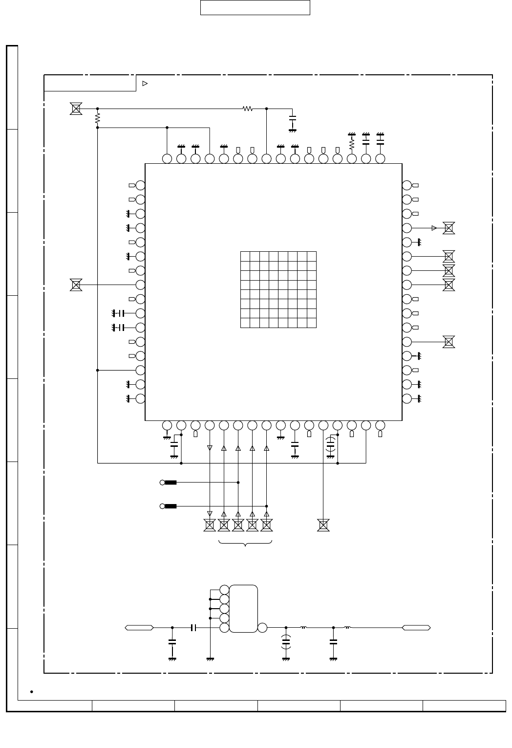
902SH
5 – 17
CONFIDENTIAL
Figure 6 SCHEMATIC DIAGRAM (6/9)
A
B
C
D
E
F
G
H
12345 6
NOTES ON SCHEMATIC DIAGRAM can be found on page 5-1.
MAIN PWB-A(6/6)
G
IRA
G
IRB
G
QRB
G
QRA
G
RXON
GQDATA
G
IDATA
GDCLK
G
VDIG275
GM_I2CDAT
GM_I2CCLK
GRESHERTA
G
SYSCLK2
SP014
SP012
NC
NC
NC
NC
NC
NC
NC
NC
NC
NC
NC
NC
NC
NC
NC
NC
NC
NC
NC
NC
NC
NC
NC
9 10111213151516
17 18 19 20 21 22 23 24
25 26 27 28 29 30 31 32
33 34 35 36 37 38 39 40
41 42 43 44 45 46 47 48
49 50 51 52 53 54 55 56
57 58 59 60 61 62 63 64
A12345678
12345678
B
C
D
E
F
G
H
VSS
VDD
IDAT
QRB
QRA
IRB
IRA
DAC03
VSS
DEC4
RXSTR
VDD
DAC02
GPA0
GPA1
VDD
VSS
DCLK
DACDAT
DACCLK
DAC01
GPA2
GPA3
GPA4
I2CCLK
RESETB
I2CDAT
QDAT
GPA6
GPA5
GPA7
DACSTR
DEC5
DEC1
REXT
VSS
AUXI1
GPCLK
GPDAT
ADSTR
AVDD
VSS
VDD
CCO
MICI P
PCMCLK
VSS
VDD
MICI N
PCMDL
VSS
VSS
BEARP
PCMUL
PCMSYN
MCLK
DEC2
DEC3
VDD
VSS
AUXO2
BEARN
NC
NC
12345789
10 11 12 13 14 15 16
17
18
19
20
21
22
23
24
25
26
27
28
29
30
31
32
33
34
35
36
37
383940
41
42
43
44
45
46
47
48
49
50
51
52
53
54
55
56
57
58
59
60
61
62
63
64
IN
GND
GND
OUT
GND
GND
1
2
3
4
5
6
BT_ANT
BU2_ANT
6
5-8 (7-F)
5-8 (12-C)
5-8 (7-F)
5-8 (12-E)
5-9 (3-A)
5-9 (3-F)
5-8 (12-E)
5-9 (3-A)
5-9 (3-F)
5-8 (9-F)
5-8 (7-F)
5-8 (12-D)
5-12 (11-A)
5-16 (11-D)
5-9 (2-E) 5-8 (10-G)
RECEPTION SIGNAL
R150
0
R151
0
C156
0.01 R140
100K
C144
0.068
C143
0.068
IC101
AB1011
GSM CODEC
C142
0.068
C141
0.068
C140
0.068
C150
0.01
CN061
BLUETOOTH
AERIAL
TERMINAL
L061
2.2nH
L061A
2.2nH
C064
1.8P
C062A
4P(CH)
C062
1.5P(CH)
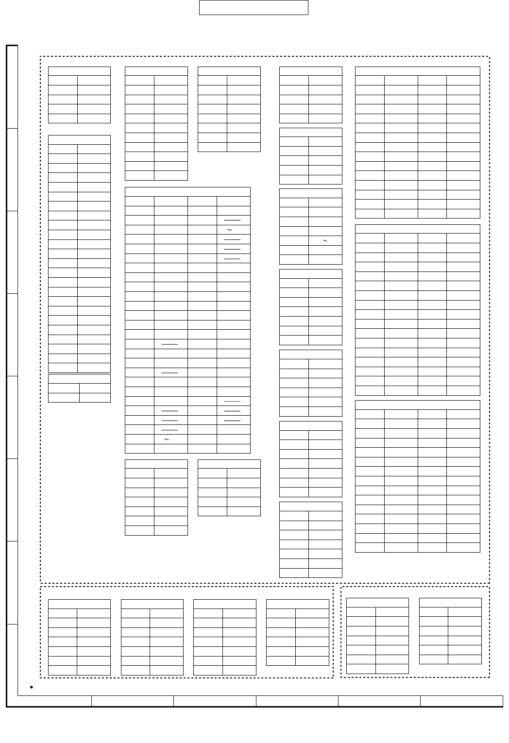
902SH
5 – 18
CONFIDENTIAL
Figure 7 SCHEMATIC DIAGRAM (7/9)
A
B
C
D
E
F
G
H
12345 6
NOTES ON SCHEMATIC DIAGRAM can be found on page 5-1.
MAIN PWB-A
DISPLAY PWB-B
IC1002
PIN NO. VOLTAGE
1
2
3
4
5
6
2.75V
0.00V
4.20V
2.89V
0.00V
38.71mV
IC2001
PIN NO. VOLTAGE
1
2
3
4
5
6
4.20V
0.00V
0.00V
0.00V
0.00V
0.00V
IC3001
PIN NO. VOLTAGE
1
2
3
4
5
6
1.85V
0.00V
4.20V
2.89V
0.00V
2.77V
IC3002
PIN NO. VOLTAGE
1
2
3
4
5
6
1.81V
0.00V
4.15V
1.85V
0.00V
2.77V
IC3004
PIN NO. VOLTAGE
1
2
3
4
5
6
1.81V
0.00V
4.16V
2.50V
0.00V
2.77V
IC1303
PIN NO. VOLTAGE
1
2
3
4
5
6
16.41mV
761.12mV
88.53mV
469.23mV
0.00V
0.00V
IC1201
PIN NO. VOLTAGE
1
2
3
4
99.11mV
18.23mV
0.00V
18.31mV
IC1204
PIN NO. VOLTAGE
1
2
3
4
1.50V
1.80V
0.00V
326.32mV
IC1205
PIN NO. VOLTAGE
1
2
3
4
1.50V
2.75V
0.00V
184.11mV
IC2004
PIN NO. VOLTAGE
1
2
3
4
5
4.20V
0.00V
0.00V
0.00V
0.00V
IC3006
PIN NO. VOLTAGE
1
2
3
4
5
3.92V
1.97V
0.00V
1.96V
3.92V
SD PWB-C
IC620
PIN NO. VOLTAGE
1
2
3
4
5
6
7
8
9
10
3.84V
2.15V
1.23V
0.78V
0.00V
0.00V
3.80V
3.84V
2.79V
0.00V
IC800
PIN NO. VOLTAGE
1
2
3
4
5
6
7
2.80V
1.66V
2.80V
0.00V
1.14V
Approx.2.78V
0.00V
IC501
PIN NO. VOLTAGE
1
2
3
4
Not Connected
0.00V
Approx.1.35V
2.79V
IC630
PIN NO. VOLTAGE
1
2
3
4
5
6
7*
8
9
10
11
12
13
14
15
16
17
18
19
20
21
22
23
2.55V
2.55V
0.00V
3.84V
3.84V
0.00V
3.70V
1.16V
0.00V
0.00V
0.00V
0.00V
0.00V
0.00V
3.70V
3.70V
0.00V
3.70V
3.70V
0.00V
0.00V
0.00V
0.00V
*
Measure condition
Tx Power
Power Voltage
21.8dbm 3.84V
IC1700
PIN NO. VOLTAGE
1
2
3
4
5
6
7
8
9
10
11
12
13
14
0.00V
2.93V
0.00V
0.00V
0.00V
0.00V
0.00V
105.21mV
0.00V
2.93V
0.00V
0.00V
2.93V
0.00V
PIN NO. VOLTAGE
15
16
17
18
19
20
21
22
23
24
25
26
27
28
0.00V
0.00V
1.02V
0.00V
0.00V
0.00V
0.00V
0.00V
0.00V
2.93V
320.61mV
161.23mV
243.21mV
325.31mV
IC1603
PIN NO. VOLTAGE
1
2
3
4
5
6
7
8
9
10
11
12
13
14
15
16
424.12mV
457.21mV
423.21mV
467.22mV
340.23mV
0.00V
265.12mV
4.20V
0.00V
229.12mV
0.00V
223.32mV
321.15mV
0.00V
176.31mV
0.00V
PIN NO. VOLTAGE
17
18
19
20
21
22
23
24
25
26
27
28
29
30
31
32
4.20V
407.21mV
621.31mV
753.11mV
0.00V
403.21mV
230.32mV
495.33mV
131.29mV
0.00V
0.00V
0.00V
2.93V
440.23mV
0.00V
0.00V
IC1504
PIN NO. VOLTAGE
1
2
3
4
5
6
7
8
9
10
11
12
13
14
0.00V
4.20V
0.00V
2.50V
4.20V
2.93V
2.89V
2.52V
4.20V
2.93V
0.00V
1.50V
1.73V
1.58V
PIN NO. VOLTAGE
15
16
17
18
19
20
21
22
23
24
25
26
27
28
1.81V
2.93V
2.89V
2.53V
2.77V
2.77V
0.00V
1.78V
4.20V
4.16V
0.00V
670mV
1.04V
1.04V
IC1602
PIN NO. VOLTAGE
1
2
3
4
5
6
4.20V
0.00V
113.25mV
0.00V
0.00V
0.00V
IC1701
PIN NO. VOLTAGE
1
2
3
4
5
6
0.00V
0.00V
0.00V
398.22mV
0.00V
209.31mV
IC1601
PIN NO. VOLTAGE
1
2
3
4
5
0.00V
0.00V
4.20V
33.20mV
0.00V
IC1206
PIN NO. VOLTAGE
1
2
3
4
5
6
4.20V
0.00V
1.80V
132 178mV
0.00V
4.20V
IC1001
PIN NO. VOLTAGE
1
2
3
4
5
6
7
8
9
10
11
12
13
14
15
16
17
18
19
20
21
22
23
24
25
26
0.00V
0.00V
0.00V
0.00V
0.00V
0.00V
0.00V
0.00V
0.00V
0.00V
0.00V
0.00V
0.00V
0.00V
0.00V
0.00V
0.30V
0.00V
0.00V
01.50V
1.80V
PIN NO. VOLTAGE
27
28
29
30
31
32
33
34
35
36
37
38
39
40
41
42
43
44
45
46
47
48
49
50
51
52
1.80V
01.80V
0.00V
0.00V
0.00V
0.00V
1.80V
2.77V
2.90V
1.80V
2.77V
0.00V
2.77V
0.00V
2.77V
1.80V
0.00V
0.00V
0.00V
902SH
5 – 19
CONFIDENTIAL
Figure 8 WIRING SIDE P.W.BOARD (1/5)
A
B
C
D
E
F
G
H
12345 6
MAIN PWB-A (FRONT SIDE)
MIC200
MIC201
SP031
SP032
SP012
SP014 SP001
SP002
SP003
SP004
1
210 20 26
515 27
1
51020253035
40
15
,
10
5,
11
20
21
9
33
1
3
2
6
4
7
8
FROM
KEY FPC UNIT
PWB-E 5-27 (2-H)
COAXIAL
CONNECTOR
COAXIAL
CONNECTOR
HINGE_B
(106-7)
HINGE_A
(106-7)
COAXIAL CABLE (106-8)
CN3001
MIC200
MICROPHONE
INFRARED DORT
To DISPLAY PWB-B
(REAR SIDE)
5-25 (3-H)
COAXIAL CABLE (161)
This PWB employs lead-free solder.
R401
R210
R211
R212
C1506
R213
C1507
C1508
C1509
R603
R604
C1510
R605
R411
C1511
R606
C1512
R1103
R220
R1104
C1514
C1515
R222
R223
IC1101 IC1100
R1109
R1110
R1111
R1112
R617
D770
R1115
C001
C002
C003
C004
R810
C005
L008
R430
IC1500
R1508
R1120
C201
R431
R1509
R1121
R626
C202
R627
LED1503
R628
C205
C012
C1684
R1127
R1128
R1512
R1514
R631
C401
R1515
R632
C402
R1516
C403
C404
R1518
R1519
C407
C022
R1520
C601
C602
R1524
R1525
C412
C413
R1527
C414
C221
C222
C223
C224
C225
C226
C227
C422
C423
C424
C425
C622
C623
C624
C431
C626
C627
C628
C631
C632
C635
C441
C442
C443
R1557
C444
C447
C448
C451
C452
C453
C454
L100
L101
R1576
FL001
Q003
L301
L110
L111
FL100
L501
L502
L503
L504
L505
L506
L507
L120
IC400
L121
L122
FL110
FL500
FL120
CN1000
L330
L331
L332
C1000
C1001
Q1001
C1006
C1007
IC620
L342
C1202
FL330
C1010
FL331
C1012
C1207
C1013
C1014
C1209
C1015
C1016
C1400
R301
R302
R303
R304
IC630
C1210
R305
L351
C1211
L352
R306
C1406
C1407
C1213
Q1210
R501
R502
R503
R504
C1410
C1651
C1220
C1221
C1222
C1223
IC1000
R701
C1225
R702
C1226
R703
R510
R511
C1229
R1012
R1013
IC1200
R326
R1016
R710
R711
L760
IC1209
C100
IC1400
R1214
C101
C102
C103
C104
R140
R335
R720
R721
C1052
C1053
R1220
R1221
R1222
R1223
C110
C111
CN901
R1225
C112
CN902
C113
R1227
R150
R1034
R151
R1037
R730
C501
C502
C503
C504
C1258
C505
C1259
C507
C313
C508
C120
R1234
C509
C121
R1041
C122
C701
C702
C703
C510
C704
R740
C511
C512
C513
C514
R1240
C515
C324
C325
C327
C328
C710
C711
R1055
C714
C715
C716
C330
C331
C332
C333
C140
C334
C141
C335
R1061
C142 R1062
C143
R1063
C144
C720
R1064
C721
R1065
R1066
R760
R1260
C341
C150
R1073
C730
R1074
C731
C156
RA1000
R770
RA1001
R771
RA1002
R772
RA1003
RA1004
C350
R1658
RA1005
RA1006
C352 C354
RA1007
RA1008
RA1009
C356
C740
C741
R1661
R1662
RA1010
R1666
C361
C362 C363
C750
C751
L200
L201
L202
L203
IC100
IC101
FL002
FL650
C760 C761
L401
IC300
C601A
C770
L411
C772
C773
FL400
IC501
C776
C777
C778
IC700
X770
L421
L422
L423
L424
L621
FL420
R002
C1104
C1106
C1107 C1108
C1109
L441
CN1501
C803
902SH
5 – 20
CONFIDENTIAL
Figure 9 WIRING SIDE P.W.BOARD (2/5)
789
10 11 12
Waveform numbers of
1
to
45 48
, are shown on pages 5-2 to 5-6.
MAIN PWB-A (REAR SIDE)
TP1601
TP1608
TP1234
TP1400
TP1215
TP1216
TP1602
TP1604 TP1605
TP1606
TP1607
TP1800 TP1611
VIB1600
VIB1601
TP1609
TP1600
TP1008
TP1010
TP1209
TP1211
TP1212 TP1219
TP1220 TP1221 TP1222
TP1610
TP1612
TP1230
TP1231
TP1232
TP1233
TP1235
SP009
SP015
SP016
SP017
SP018
SP019
SP020
SP028
SP029
TP1302
TP1304
TP1507
TP1210
TP1021
TP1218
TP1228
SP021
SP023
TP1303
TP1305 TP1306
TP1307
SP008
SP022
TP1003
TP1229
SP027
TP1023 TP1236
TP1237
TP1019 TP1020
TP1226
TP1227
TP1500
TP1501
TP1502
TP1504
TP1505
TP1006
TP1009
TP1206
TP1013
TP1015
TP1016 TP1017
TP1018
TP1024
TP1225
TP1613
TP1308
TP1022
TP1004
TP1005
TP1007
TP1011
TP1012
TP1014
TP1223
TP1614
TP1503
TP1200 TP1201
TP1202
TP1203
TP1204
TP1205
TP1207
TP1603
TP1301
TP1506
TP1213
TP1002
TP1217
1
5
10
15
20
25
35
40
45
50
30
26
1
1
8
9101516
17
20
24 25 30
32
5
3
4
6
1
51013
14
16 15
18
1
52
5
10
13
14
1520
1
1
1
3
3
4
4
6
6
2
3
4
25
27
28
30
35
40
41
45 50
1
1
1
5
10
1
3
4
5
3
3
6
75
8
10
14
15
21
20 22
25
28
1
1
3
23
1
5
7
8
14
15
20
21
22 25
28
10
4
4
6
1
3
1
2
34
4
6
BUILT-IN
AERIAL
TERMINAL
BUILT-IN AERIAL
17
19
1
2
3
BLUETOOTH
AERIAL TERMINAL
BLUETOOTH AERIAL
PWB-K
USIM CARD CONNECTOR
EXTERNAL
CONNECTOR
CHARGE
TERMINAL
CHARGE
TERMINAL
BATTERY
TERMINAL
VIDEO OUT/
HANDS FREE
MICRO PHONE
CONNECTOR
SMALL LIGHT
5-27 (3-C)
FROM
SD P.W.B.
CONNECT
FPC PWB-H
12 13
,
16 17
,
14 15
,
44
34
45
26
27
35
43
29
28
31
48
M
25
33
38
41
19
18
36
32
30
39
23
40
42
24
37
This PWB employs lead-free solder.
22
VIBRATOR
V1500
V1501
C1502
C1503
C1504
C1505
V1311
C1700
C1701
C1702
C1703
R1100
C1704
R1101
C1705
R1102
C1706
C1707
C1513
R1106
C1516
R1107
C1517
R1108
C1518
C1519
IC1103
R1300
IC1104
R1301
IC1105
R1302
IC1106
R1303
C1713
R1304
C1714
C1520
C1521
R809
R1305
C1716
R1306
R1307
C1717
C1523
IC1300
R1308
R1114
C1718
C1524
R1309
C1525
C1526
IC1303
C1527
L1500A
C1528
R811
L1501
R1119
C1529
R1502
R1503
C007
R1504
R1310
C1720
R1505
C1721
R1312
R1506
C1722
R1507
C1723
C1530
R1315
C1531
IC1502
R1316
C1532
R1317
IC1504
CA1521
IC1505
R1704
R1510
L1201
R1511
IC1700
IC1701
R1517
R1130
C1542
R1711
C023
L061A
C062A
R1716
R1522
R1717
R1523
R1718
R1719
R1526
L1600
R1528
L1601
R1529
V1551
L1602
V1552
R1603
V1553
C800
C1554
R1720
C801
C1555
C802
R1606A
R1723
R1724
R1530
R1531
R1532
R1533
R1534
R1537
R1538
R1539
CN061
R1540
R1541
R1542
R1543
R1544
R1545
R1546
R1547
R1548
R1549
R1550
R1551
R1554
R1555
R1556
FS1200
R1558
R1559
C1582
L061
C062
C1587
C064
R1560
R1561
R1562
R1563
R1564
R1565
L1566
L1567
FL1500
FL1501
R1570
R1571
R1572
R1573
R1574
R1575
RA1500
R1578
JK1600
Q701
LED1200
L904
L906
IC800
CN1200
ANT901
CN1201
C1002
C1003
Q1000
C1004
C1005
C1008
C1009
RA1547
C1200
C1201
C1203
Q1200
C1204
Q1201
C1205
C1011
C1206
Q1203
C1208
Q1206
C1017
Q1208
C1401
C1402
C1403
C1404
C1405
C1212
C1408
C1214
C1409
Q1211
C1215
C1216
Q1212
C1217
C1600
X1500
D1000
C1218
Q1214
RA1561
C1601
Q1215
C1602
C1603
C1604
C1028
C1605
Q1601
C1411
C1029
Q1602
C1606
C1412
C1413
C1607
C1414
C1608
C1415
Q1605
V1416
D1200
C1800
C1224
C1030
IC1001
D1201
C1801
C1031
D1202
IC1002
C1802
C1032
D1203
IC1003
C1803
C1227
IC1004
C1610
R1200
C1034
C1611
R1201
C1035
IC1005
C1612
C1036
R1203
C1613
C1037
C1614
C1038
R1011
R1205
R1206
R1207
R1208
R901
IC1201
C1619
R1209
IC1202
C1232
R902
IC1203
R1017
IC1204
C1040
CA1609
R1401
IC1205
C1235
C1041
R1402
IC1206
C1236
R1403
R1210
C1620
C1238
R1211
V1045
C1621
C1239
R1212
C1622
V1047
R1213
C1623
D1600
R1020
C1624
IC1401
D1601
R1215
R1021
C1625
V1602
R1216
C1626
D1603
R1217
R1023
C1627
R1218
R1024
C1628
C1241
R1219
R1025
C1629
R1602
R1026
C1244
C1050
R1029
C1051
C1245
R1606
C1246
C1247
R1607
IC1600
C1630
IC1601
R1609
C1631
C1249
C1632
IC1602
IC1603
C1633
R1224
R1030
C1634
C1635
R1613
R1616
R1615
R1031
R1802
R1226
R1032
R1803
R1033
C1637
R1300A
R1804
R1610
C1250
R1301A
R1611
R1229
R1035
C1251
R1806
R1302A
R1612
R1036
C1252
R1807
R1303A
C1253
V1117
IC1800
R1304A
R1614
R1038
R1039
C1255
R1306A
R1617
R1618
R1230
C1228
C1231
C1230
C1640
R1619
R1232
C1642
L1500
R1040
C1644
R1235
C1645
R1042
C1646
R1237
C1647
C1648
R1620
R1238
C1260
R1045
R1621
R1239
R1622
R1046
R1623
R1047
R1048
R1624
R1049
R1625
R1626
R1627
R1628
C1650
R1241
C1652
R1242
V1653
C900
L907
L908
R1244
R1050
C1654
R1245
R1051
C1655
C902
R1246
R1052
R1247
R1053
R904
R1248
R1054
R1630
R1631
C905
R1056
R1057
R1634
R1058
R1059
R1266
R1635
R1636
R1638
R1639
C1664
R1060
C1665
R1255
C1666
R1256
C1667
R1258
R1641
R1642
R1067
R1643
R1644
R1069
R1645
R1646
R1648
C1671
R1261
R1649
C1672
R1262
C1673
R1263
R1070
C1674
R1264
R1071
C1675
R1265
C1676
C1677
C1678
R1650
R1075
C1679
R1651
R1076
R1652
R1653
L1654
R1077
R1655
R1656
R773
R1657
R774
C1680
C1681
R1659
C1682
R1660
R1663
R1664
R1665
R1667
R1668
L001
RA1017
RA1018
R1673
R1678
R1679
RA1027
RA1028
FL003
RA1800
C779
CN1300
X1000
RA1647
CN1500
C1300
C1301
C1302
C1303
C1304
C1110
C1305
Q1301
C1111
C1306
C1112
C1307
C1113
C1116
Q1002
R1068
Q1604
IC1604
C1709
Q1202
Q1204
Q1205
Q1213
Q1207
Q1209
C1240
Q1300
VIB001
CONFIDENTIAL
5
--
21 5
--
22
Figure 10 SCHEMATIC DIAGRAM (8/9)
902SH 902SH
A
B
C
D
E
F
G
H
12345 6789
10 11 12
NOTES ON SCHEMATIC DIAGRAM can be found on page 5-1. ( ) : Not Mount Waveform numbers of
4746
,
49
,
50
, are shown on pages 5-2, 5-3.
DISPLAY PWB-B
TP3009
TP3012
TP3002
TP3025 TP3008
TP3018
TP3024
TP3053
TP3
TP4
TP5
TP6
TP7
TP8
TP9
TP10
TP11
TP12
TP13
TP14
TP15
TP16
TP17
TP18
TP19
TP20
TP21
TP22
TP23
TP2
TP1
TP3054
TP3055
TP3033
TP3031
TP3032
TP3049
TP3051
TP3048
TP3050
TP3003
TP3004
TP3005
TP3056
TP3057
TP3059
TP3058
TP3061
TP3063
TP3062
TP3060
TP3064
TP3066
TP3065
TP3067
TP3068
T-COM
T-COM
TFT-COM
COMC
COMC
COMDC
VCOMH
B0
B1
B2
B3
B4
B5
G0
G1
G2
G3
G4
G5
R0
R1
R2
R3
R4
R5
DCLK
HSY
VSY
SO
SI
SCLK
CS
RESET
VCC
GND
GND
VDC
VDC
COM2
VCL AM
VSS2
VSS1
NC
VDD2
C5-
C5+
C4-
C4+
C3-
C3+
C2-
C2+
C1-
C1+
VDC2
VDC2
VR
VS
VS
60
61
3
5
49
39
29
19
9
52
42
33
41
31
21
11
54
44
34
6
7
1
23
13
2
56
46
36
26
59
50
15
58
48
38
28
18
8
51
4
40
30
20
10
53
43
32
22
12
55
45
35
25
16
24
14
57
47
37
27
17
NC
NC
NC
NC
NC
NC
NC
NC
NC
NC
NC
NC
NC
NC
NC
NC
NC
NC
NC
NC
NC
NC
NC
NC
NC
NC
NC
NC
NC
NC
NC
NC
NC
NC
NC
NC
NC
NC
NC
NC
NC
NC
NC
NC
NC
NC
NC
NC
NC
NC
NC
NC
NC
NC
NC
NC
NC
NC
NC
NCNC
1
2
3
4
5
RXCKN
60
14
VDDPLL
149
VDDIOA
VDDIOD
1
105
25
52
176170
2
K
86
28 32
O
168165
118
7
SUBCK/SUBGPO1
GNDPLL
SUBDB0
DB11
GND
76
BSPIXEL2/NDATA2
DB0
GPO9
BSVS_B/VSYNC_NT
SCL
158
12
F
GDATA2
8
55
GSR
PLLDIV2
VDDOSC
167
VDDIOD
161
6259
9
103
16
126
111
92
73
109
65
3
38 43
8785
SUBRS/SUBGPO2
SCANEN
SUBDB1
DB10
GND
82
BSPIXEL3/NDATA3
DB1
GPO10
110
1
BSHS_B/HSYNC_NT
GPO0
GDATA3
VDWAIT_B
PLLDIV1
97
VDDCORE
VDDIOB
175
37
145
M
160
34
117
102
15
58
142
113
TESTI
144
SUBDB2
DB12
GND
80
DB3
GPI0
GPO1
GDATA0
143
RESET_B
PLLDIV0
VDDCORE
VDDIOB
95
40
DCLK
77
172
127
57
71
41
C
151
91
26
54
D
9
SUBCS_B/SUBGPO3
GPCLK
SUBDB3
DB8
GND
DB2
GPI1
169
G
GPO2
GDATA1
BDATA5
BDATA4
XIN/SCANCK
152
124
23
VDDCORE
22
VDDIOA
HSYNC
53
119
146
49
171
115
88
48
SE_LD2/PORT3
78
45
6
101
SUBDB4
DB13
GND
13
BSPIXEL6/NDATA6
DB5
GPI2
GPO3
RDATA5
130
50
134
10
OSCIN
VDDCORE
174
VDDIOB
VSYNC
100
39
81
11
14
5
93
20
122
11
147
162
98
A2
SUBWR_B/SUBGPO4
SE_LD3/PORT4
I
SUBDB5
MAGBUSY
GND
96
BSPIXEL4/NDATA4
DB7
WAIT_B
GPI3
BSPIXEL0/NDATA0
GPO4
H
B
RDATA4
BDATA2
OSCOUT
VDDCORE
13
108
VDDIOA
SE_DI/PORT6
84
68
163
157
66
120
56
5
19
164
129
114
SE_LD4/PORT5
SUBDB6
NTCLK
GND
153
DB6
BUFOFF_B
GPI4
GPO5
RDATA2
BDATA3
131
VD0N
VDDCORE
VDDIOC
SE_DO/PORT0
E
15
31
4
94
136
44
132
4
79
135
47
133
SUBRD_B/SUBGPO5
PWM0/PORT7
SUBDB7
BSCLK/DCLK_NT
GND
BSPIXEL5/NDATA5
DB4
CS_B
GPI5
GPO6
3
8
33
RDATA3
116
GDATA5
RXDTP
VDDCORE
148
46
VDDIOC
150
69
SE_CK/PORT1
154
18
70
166
104
137
72
10
PWM1/PORT8
SUBCKS/SUBGPO0
GND
128
42
BSPIXEL7/NDATA7
DB15
RD_B
GND
138
P
16
BSPIXEL1/NDATA1
GPO7
N
RDATA0
GDATA4
RXDTN
61 63
VDDCORE
VDDIOA
173
SE_LD1/PORT2
24
112
6
35
139
64
21
125
74
29
83
SUBFLMIN
PWMLCD/PORT9
159
140
J
GNDOSC
L
DB14
WR_B
GND
90
GPO8
RDATA1
7
30
BDATA0
RXCKP
VDDVD
75
VDDIOB
89
51
VDDIOB
17 27
106 107
156
12
141
99
67
121
155
36
SUBLPIN
LCDINT
GNDVD
BSBLK_B
DB9
RSP
GND
123
GPO11
SDA
BDATA1
LR38866
NC
NC
NC
NC
NC
NC
NC
NC
NC
NC
NC
NC
DUMMY
DUMMY
DUMMY
DUMMY
1
2
34
5
6
7
8
910
11
12 13
14
15
16
17
18
19 20 2122
23
24
25 26 27 28 29
30
31
32
33
34
35
36
3738
39
4041 42
4344 45 46 47
48
49
50
51
52
5354 55 56
57 58
59
60
61
62
63
64
65
66
67
68
69
70
7172
73
74
75
76
77
78
79
80
81
82
83
84
85
86 87
88
89
90
101
102
103
104
105
106
107
108109
110 111
112
113
114
115
116 117118
119
120
121
122
123
124125 126
127
128
129
130
131
132
133
134
135
136
138 139140
141 142
143
144
145
146
147
148
149
150
151
152
153
154
155
156
157 158
159
160
161
162
163
164
165
166
167
168
169
170
171
172
173174
175
176
96
91
95 94
99
98
93
100
92
97
137
VBATIB
VUDIG29
VUDIG18
VUDIG29
VUDIG25
VUDIG29
VUDIG25
VUDIG18
VUDIG29
VBATIB VUDIG29
VUDIG29 VUDIG18
VUDIG29
VUDIG18
VCCR
VUDIG29
VUDIG18
VUDIG18
1
2
34
5
3
40
E
64
35
959488
105
J
15
47
79
A
91
22
108
27
73
30
9
1
77
69
3
G
25
1
99
48
67
52
70
107
6
49
86
104
14
87
8
65
24
93
20
75
66
43
D
51
98
72
12
4
2
84
57
M
81
37
58
31 32
63
38
B
41
K
34
19
29
11
59
46
76
6
F
21
54
74
7
102 106
5350
12
92
68
4
10
33
62
10
78
5
16
8
23
82
42
56 60
100
28
85
80
89
17
9
26
97
71
96
2
61
36
7
13
5
45
39
103
90
44
H
11
18
C
101
L
55
83
DCLK
HSYNC
VSYNC
R0
R1
R2
R3
R4
R5
G0
G1
G2
G3
G4
G5
B0
B1
B2
B3
B4
B5
SCLEG0
SCLEG1
SCLK
SCS
SDI
SDO
NRESET
EDO
EDI
ECLK
ECS
C1P
C1N
C2P
C2N
C3P
C3N
C4P
C4N
VDC2
VIN2
V49_OUT
VDD_AIO
V51_OUT
PVOPL
PVOPH
PVONL
PVONH
NC
VIN
VDD_DIO
VDD_DIO
VDD_DCORE
VDD_DCORE
VDD_PLL
V18_SEL
V18_OUT
GND_D
GND_D
GND_D
GND_PLL
GND_DC1
GND_DC2
GND_DC3
GND_VREF
GND_5
GND_DAC1
GND_DAC2
GND_DAC3
COM
VEE_OUT
GSPB
GCK
UD
GOE
INIT
VDD_OUT
SSPB
SCK
SCKB
PCTL
PVOUT
LR
AVOUT1_R
AVOUT2_R
AVOUT3_R
AVOUT4_R
AVOUT1_G
AVOUT2_G
AVOUT3_G
AVOUT4_G
AVOUT1_B
AVOUT2_B
AVOUT3_B
AVOUT4_B
EXT1
TEST0
TEST1
TEST2
TEST3
STATUS0
STATUS1
NC1
NC2
NC3
NC4
EXT2
RH-IXA040AF01L
1
2
3
4
5
6
7
8
9
10
11
1213 14
15
16
17
18
19
20
21
22
23
24
2526
2728
2930
3132
33
3435
36
3738
3940 41
42
4344 45
46
47
48
49 50
51
52
53
54
55
56
57
58
59
60
61
62
63
6465
66
67
68
69
70
71
72
73
74
75
76
77
78 79 80
81
82
83
84
85
86
87
8889
90
91
92
93
94
95
96
97
98
99
100101
102
103
104
105
106
107
108
1
2
3
4
5
6
7
8
9
10
11
12
13
14
15
16
17
18
19
20
21
22
23
24
25
26
27
28
29
30
31
32
33
34
35
36
37
38
39
40
41
42
1
2
3
4
5
7
6
8
9
10
11
12
13
14
15
16
17
18
19
20
21
22
23
24
25
26
27
28
29
30
31
IN1
OUT1
IN2
OUT2
IN3
OUT3
IN4
OUT4
GND
GND 1
2
3
4
5
6
7
8
9
10
IN4
OUT4
IN3
OUT3
IN2
OUT2
IN1
OUT1
GND
GND
1
2
3
4
5
6
7
8
9
10
1
2
3
4
1234
5678
1234
5678
TP3036
TP3035
TP3034
NC NC
VUDIG29
VCCR
TP3019
TP3037
TP3010
TP3026
TP3027
TP3028
TP3011
TP3007 1
2
3
4
5
6
7
8
9
10
VBATIB
VUDIG25
VBATIB
VUDIG29
VUDIG18
1
2
3
45
6
7
81
2
3
45
6
7
8
1
2
3
45
6
7
8
1
2
3
45
6
7
8
1
2
3
45
6
7
8
1
2
3
45
6
7
8
1
2
3
45
6
7
8
1
2
3
45
6
7
8
1
2
3
45
6
7
8
1
2
3
45
6
7
8
1234
5678
1234
5678
EAR
XEAR
LCDRST
LCDINT
R3
R1
R2
R0
R4
R5
B0
B1
B2
B3
B4
B5
G0
G1
G2
G3
G4
G5
R0
R1
R2
R3
R4
R5
R0
R1
R2
R3
R4
R5
G0
G1
G2
G3
G4
G5
B0
B1
B2
B3
B4
B5
DCLK
DCLK
SP-R2
SP-R1
SP-L2
SP-L1
SE_DI_
LVSIN
VDON
VDWAIT
M_LCD_I2CCLK
M_LCD_I2CDAT
LVSIN
LCDCLK
TXDTP
TXDTN
TXCKP
TXCKN
VDWAIT
M_LCD_I2CDAT
M_LCD_I2CCLK
SE_LD1
SE_LD1
SE_CK
SE_CK
SE_DO
SE_DO
HSYNC_M
HSYNC_M
VSYNC_M
VSYNC_M
LCDIN T
LCDRST
XRESET
BD4
BD5
BD2
BD1
GD0
GD2
BD0
BD3
GD4
GD1
GD5
GD3
RD3
RD1
RD2
RD0
RD4
RD5
BD5
BD3
BD2
BD1
BD4
GD2
GD3
GD0
GD4
GD5
GD1
BD0
RD3
RD1
RD2
RD0
RD4
RD5
B0
G1
G5
G4
G0
G3
G2
B4
B1
B2
B3
B5
SE_DI
XRESET_
D7
D6
D4
VSYNC
PCLK
VDON
D5
HSYNC
I2CCLKA
I2CCLKA
I2CDATA
I2CDATA
PCLK
HSYNC
VSYNC
D3
D1
D0
D2
D1
D0
D3
D4
D6
D5
D7
D2
POW_ECO
LCDRST_M
LCDRST_M
POW_CE
TXDTN
TXDTP
TXCKN
TXCKP
VDD
OUT
GND
SP2001
STEREO
SPEAKER (R)
SP2000
STEREO
SPEAKER (L)
EP1000
EARPIECE
BATT1200
BACK-UP
BATTERY
2.2K
LCD-C BUS &etc
SUB CAMERA BUS
MR SENSOR
D5(CAMPXL0)
SDA(CAM)
D7(CAMPXL0)
PCLK
D3(CAMPXL0)
SCL(CAM)
XI
D4(CAMPXL0)
D1(CAMPXL0)
RSTB
D6(CAMPXL0)
D0(CAMPXL0)
HSYNC
D2(CAMPXL0)
GND
ECO
VDD
GND
CE
Vout
GND
VDD
ECO
GND
Vout
CE
TCOM2
GVSS
GSPB
GCK
UD
GOE
INIT
VDD
SSPB
VSS
SCK
SCKB
PCTL
PVID2
PVID1
LR
VR1
VR2
VR3
VR4
VG1
VG2
VG3
VG4
VB1
VB2
VB3
VB4
TCOM1
A
B
C
D
CORE
VCC
GND
ESD
VSYNC
AVDD
AGND
CREFP
CREFN
STDBY
DVDD
HVDD
DGND
VCCR
SP-R2
VCC
SP-R1
GND
FLIP_R
SP-L2
SP-L1
SPEAKER FPC
PWB-G
LED FPC UNIT
PWB-F
GND
VoutVDD
CE ECO
GND
6
1
2
34
5
6
1
2
34
5
6
IN4
OUT4
IN3
OUT3
IN2
OUT2
IN1
OUT1
GND
GND 4
3
2
1
8
7
6
5
10
9
FROM
COAXIAL
CABLE
5-12 (12-E)
46
47
,
5049
,
5049
,
5049
SUB CAMERA UNIT PWB-D
LCD3000
MAIN DISPLAY
RECEPTION SIGNAL
SPEAKER SIGNAL
BATTCAM
BLED-
D5(CAMPXL0)
SCL(CAM
BATTLCD
SP-R2
VTX1DP
D0(CAMPXL0)
HSYNC
D7(CAMPXL0)
SDA(LCD
SP-L2
LVSIN
D1(CAMPXL0)
LCDRST
SDA(CAM
POW_CE
D2(CAMPXL0)
D3(CAMPXL0)
BLED+
VTX1CKP
FLIP_R
SP-L1
VSYNC
SYSCLK
XEAR
D4(CAMPXL0)
VTX1CKN
LCDINT
SUBCAMTEMP
SP-R1
PCCLK
POW_ECO
VDON
VTX1DN
D6(CAMPXL0)
VDWAIT
VCCR
SCL(LCD
EAR
IXA040
R3051
1
R3002A
0
R3052
1
R3003A
0
R3053
1
R3000A
0
R3054
1
R3001A
0
C3011
470P (CH)
C3010
470P (CH)
C3005
470P (CH)
C3004
470P (CH)
C3089
15P (CH)
C3090
15P (CH)
R3000
8.2
R3037
8.2
R3016A
0
R3017A
0
C3002
15P (CH)
C3003
15P (CH)
R3008A
0
R3008
0
R3015
1K
C3034
0.1
C3071
0.001
C3035
0.1
R3010
0
C3036
0.1
R3044
0
R3002
0
R3004
10
R3003
10
C3032
0.1
R3056
100
C3038
0.1
L3011
82nH L3012
82nH
L3009
82nH
L3010
82nH
R3014
220K
R3012
100
R3013
100
V3143
100P
R3026
0
R3100
0
C3019
1C3020
1
R3001
0
C3025
1
R3103
0
C3026
1
R3104
0C3043
1
C3042
1
R3106
0
R3107
0
C3065
0.1
R3023
0
R3025
0
R3040
10
FL3001
EMI FILTER
R3016
0
FL3002
EMI FILTER
FL3003
EMI FILTER
C3064
4.7
C3063
2.2
R3038
0
C3062
4.7
C3070
4.7/10
C3069
4.7
C3068
1
C3067
1
C3056
10
C3060
100P
(CH)
R3063
0
C3055
4.7
C3066
4.7
R3021
56K
R3062
0
C3072
10
C3053
10
R3019
0
R3009
0
C3044
15P (CH)
R3018
100
C3052
0.01
R3055
1M
R3024
100
R3017
100
R3006
0
C3013
10
C3112
10
C3111
10
C3012
10
D3000
RB521S30
C3058
1
C3057
1
C3059
100P (CH)
C3050
1/16
IC3006
TC7SZ08F
LOGIC
CN3001 D3003
RB520S30
RA3010
100
RA3011
100
RA3012
100
RA3013
100
D3002
RB521S30
IC3000
LR38866
DISPLAY
CONTROLLER
IC3004
R1162D251D
REGULATOR
V3018
100P
CN3003
IC3001
R1162D291D
2.9 V REGULATOR IC3002
R1162D181D5
REGULATOR
C3083
0.1
R3059
0
CN3000
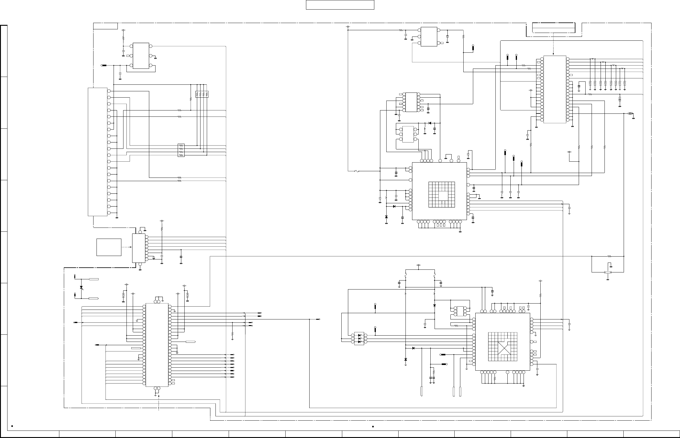
CONFIDENTIAL
5
--
23 5
--
24
Figure 11 SCHEMATIC DIAGRAM (9/9)
902SH 902SH
A
B
C
D
E
F
G
H
12345 6789
10 11 12
NOTES ON SCHEMATIC DIAGRAM can be found on page 5-1. ( ) : Not Mount
SD PWB-C
NC
NC
NC
NC
NC
NC
NC
NC
NC
NC
NC
NC
NC
NC
NC
NC
NC
NC
NC
NC
NC
NC
5-24 (8-H)
5-24 (8-H)
5-24 (8-H)
5-24 (9-H)
5-23 (2-E)
FROM
SD P.W.B CONNECT
FPC PWB-H
5-11 (2-H)
5-23 (2-F) 5-23 (4-G)
TP2003 TP2005
STRB
SENSN1
SENSN2
TEST2
TRSW
VBAT1
DATA
CURSENS
T4
VBATP
CNTOUT
GNDT3
VIO
SENSP1
VIN
TEST
VOUT1
VBAT2
GNDP
VPLUS12
SENSP2
VOUT2
1
A
B
C
D
E
F
G
108149
15 17
19
18
21
23
22
25
27
26
32
34
33
38 3937
13
36
1211
16
20
24
31
35
28 29 30
40
NC
VNEG
GND1
SW
CAMP
REG1CNT
REG2CNT
GNDT1
RSTB
CLK
GND2
VPLUS11
CUR
T2
VREF
VSEL2
GND3
VBAT3
2
4
10
11
12
13
14
15 16
17
18
19
20
21
22
26
27
34
36
37
38
40
39
23 8
13
9
30
35 6
31
5
7
33
32
29
25
24 28
TP2006
TP2004
NC
NC
NC
GND
PD
NC
VSEL
VBAT
VSUB
VNEG
NC
VOUT
NC
NC
2
3
5
4
67
8
9
10
11
12
1
1
2
3
4
5
6
7
8
9
10
11
12
13
14
15
16
17
18
19
20
21
22
23
24
25
26
27
28
29
30
31
32
33
34
35
36
37
38
39
40
SEDO
SECLK
DC_B
RESETB
SCEB
VDD
GND
VLCDIN
1
2
3
4
5
6
7
8
9
10
BLED-
1
2
3
45
TRSW
SENSP
SENSN
VPLUS2
LEDR
LEDG
LEDB
SW
VPLUS11
VPLUS12
BLED
FLED
SBD
VNEG
T1
T2
T3
T4
IREF
TEST
GND1
GND2
GND3
GNDP
LEDCTL
VREF
WVOUT
LSO12
LSO11
ERROUT
FRP
CLK
STRB
DATA
RSTB
VBAT1
VBAT2
VIO
CPIN
CAPP1
CAPN1
CAP3
CAMP
CAMN
12
A
B
C
D
E
F
G
H
12109
15
11
1716 1918
2120 2322
2524 2726
2928 3130
3332 3836 3735
424039 4644 4541 43
13 14
34
CAPP2
CAPN2
1
2
3
4
5
6
7
8
10
11
12
13 14
15
16
17
18 19
20
21
22
23
24
25
26
27
28
29
30
31
32
33
34
35
36
37
38
39
40
41
42
43
44
45
46
TP2000
TP2001
SLED-
BLED+
BLED-
BLED+
SLED-
BLED+
1
2
3
45
1
2
3
4
5678
1
2
3
45
6
7
8
NC
VSS(GND)
VDD
COM
SDDAT3
SDDAT0
SDCLK
SDCMD
VSS(GND)
SDDAT1
SDDET_N
SDDAT2
SDPWR
VDD
VSS(GND)
GND
GND
GND
GND
GND
GND
1
2
3
4
56
7
89
10
11
1213
14
15
16
17
18
19
20
TP2002
TP2007
TP2008
GREEN
RED
BLUE
1
2
34
5
6
TP2014
TP2009
TP2010
TP2011
TP2012
TP2013
TP2015
TP2016
TP2017
TP2020
TP2019
TP2021
TP2018
TP2022
TP2023
TP2024
TP2025
TP2026
1
2
3
4
56
7
8
9
10
11
1213
14
15
16
17
18
19
20
21
22
23
24
25
26 27 28 29 30 31 32 33 34 35 36 37 38 39 40 41 42 43 44 45 46 47 48 49 50
51
52
53 54
TP2027
D
G
D
D
S
D
1
2
34
5
6
D
D
S
D
G
D
1
2
34
5
6
SLCDDC
SECLK
SEDO
SDDET_N
SDPWR
SDCLK
SDCMD
SDEN
SECLK
LEDLD
SEDO
SECLK
SEDO
BDCE
RSTGA
I2CCLKB
FLOW
I2CDATB
GAINT
SLCDCE
VRX2DP
VRX2DN
SLCDRST
SDEN
SDDET_N
SDCLK
SDDATA2
SDDATA3
SDDATA0
SDDATA1
SDCMD
SDPWR
ZMPEN
VRX2DP
VRX2DN
VRX2CKN
VRX2CKP
VRX2CKP
VRX2CKN
SDDATA0
SDDATA1
SDDATA2
SDDATA3
LEDLD
I2CCLKB
I2CDATB
TXON_N
GAINT
SEDO
SECLK
BDCE
BDRST
SLCDRST
SLCDDC
SLCDCE
LEDRST
RSTGA FLOW
ZMPEN
LEDRST
BDRST
CKN
CKP
DN
DP
PW-CLK
STBY-P2
SCL
Y7
Y5
Y3
Y1
RSTN
VS
AVDD
VDD(1.8V)
HIOVDD
GND(DSP)
EXCKI
GND(DSP)
RCLKGND(DSP)
CIOVDD
AGND
DSP_INT2
STSEL1
DAS
HREF2
IOCTRL
Y0
Y2
Y4
Y6
SDA
STBY-P1
STBYP3
VDD(DRIVER)
VL(-8V)
VH(+15V)
NC
GND(DRIVER)
NC
CE
GND
ECO
VIN
VOUT
MOBILE LIGHT
BDCE
SDDATA1
FLOW
SDPWR
SCEB
GAINT
DC_B
RSTGA
SDDATA0
BATTBB
SDDET_N
SLCDRST
BLED+
LEDLD
BATTBB
SDDATA3
TXON_N
LEDRST
SDCMD
BDRST
BLED-
SDEN
SDDATA2
EXCKI
SDCLK
ZMPEN
SEDO
I2CCLKB
(2MCAM)
I2CDATB
(2MCAM)
SECLK
LVDSCKN
LVDSCKP
LVDSDN
LVDSDP
VCC
VCC
GND
GND
VOUT1(3.0V)
VOUT2(1.8V)
VDIG29(2.9V)
VDD4(-8V)
VDD3(+15V)
BATTBB
BATTBB
BATTBB
GND
GND
GND
GND
MIAN/SUB LED+
SUB LED-
MAIN LED-
GND
VDOUTEN
VIN
VSS
VROUT
VCC
VCC
SP+
SP-
6
34 5 67 8
1234 567 8
234567
12345 67
VBATIB
VBATIB
VDIG29
VBATIB
VDIG29
VDIG29
VBATIB
VDIG29
VBATIB
VDIG29
VDIG29
LCD2000
SUB
DISPLAY
CAMERA UNIT PWB-J
9
R2023
0
C2000
4.7
IC2001
R1161D291D
SD POWER
CONTROL
C2001
4.7
CN2001
MEMORY CARD
CONNECTOR
R2004
10K
R2002
47
R2003
0
R2006
100K
R2001
100
R2000
100
R2022
100
R2005
0
CN2003
C2031
0.1
C2004
0.1
C2003
0.1
LED2006
NECW008A
WHITE
CN2000
R2012
10K
LED2005
GM56281A
D2002
RB520S30
D2000
RB520S30
C2007
1
D2004
RB551V30
C2019
4.7
C2008
4.7
L2001
4.7µH
L2003
4.7µH
Q2005
MCH6413
R2009
0.1
R2008
3.3
C2012
2.2
C2009
0.47
R2011
120K
IC2005
BD6015GU
COMPOUND POWER SUPPLY 1
C2025
0.1
C2045
0.1
R2013
0
C2024
0.1
C2018
4.7
R2024
0
C2046
0.1
C2027
1
C2028
4.7
C2029
4.7
C2023
0.1
C2022
0.1
IC2002
BD6020
COMPOUND
POWER SUPPLY 2
C2021
2.2
C2017
4.7
L2004
4.7µH
D2005
RB551V30
FS2002
1.25A
FS2001
0.63A
Q2002
FDG312 P
C2015
1
C2013
0.1
IC2003
BD6030
COMPOUND
POWER SUPPLY 3
C2011
4.7
FS2000
1.25A
C2010
4.7
L2002
4.7µH
C2006
4.7
D2003
RB520S30
C2014
0.47
D2001
RB520S30
R2016
0
C2026
1
R2018
0
R2019
0
R2020
0
R2017
1K
C2047
0.1
L2006
82nH
L2008
82nH
L2005
82nH
L2007
82nH
CN2002
R2015
0
R2014
0
R2021
0
C2020
1
IC2004
XC640231
REGULATOR
C2016
1
R2010
0
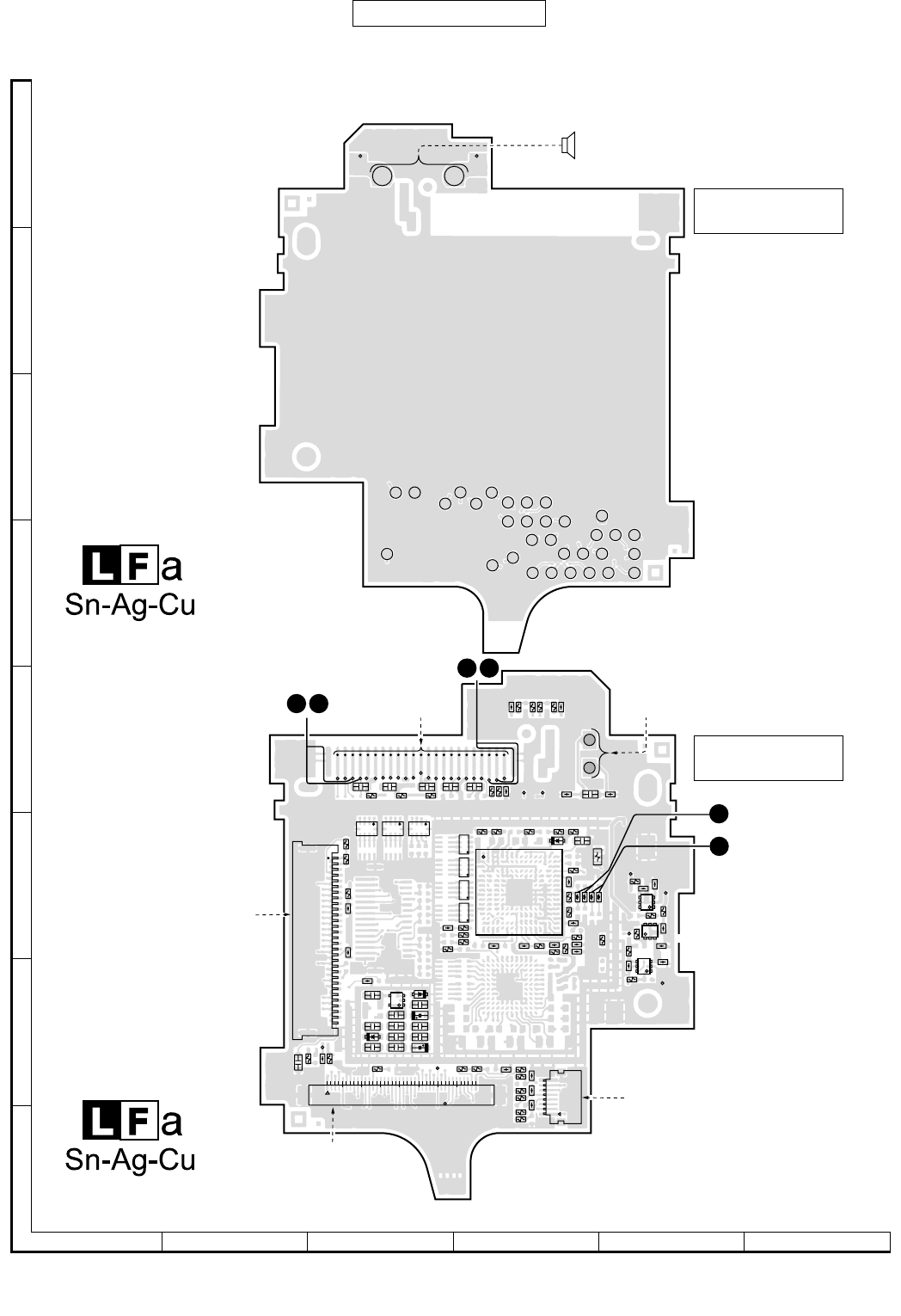
902SH
5 – 25
CONFIDENTIAL
Figure 12 WIRING SIDE P.W.BOARD (3/5)
A
B
C
D
E
F
G
H
12345 6
TP3002
TP3003
TP3004
TP3005 TP3012
TP3019
TP3025
TP3031
TP3032
TP3033
TP3034
TP3035
TP3036
TP3037
TP3048
TP3049
TP3050
TP3051
TP3053
TP3056
TP3057
TP3058
TP3059
TP3060
TP3061
TP3062 TP3063
TP3064
TP3065
TP3066
TP3067
TP3068
TP3008
TP3009
TP3010
TP3026
TP1
TP2
TP3
TP4
TP5
TP6
TP7
TP8
TP9
TP10
TP11
TP12
TP13
TP14
TP15
TP16
TP17
TP18
TP19
TP20
TP21
TP22
TP23
TP3007
TP3011
TP3027
TP3028
TP3018
TP3024
TP3053
TP3054
TP3055
1
1
1
3
3
3
4
4
4
6
6
6
1
8
1
2
10
20
30
40
50
5
15
25
35
45
55
59
15 10152025
30 35
40
EP1000
EARPIECE
DISPLAY PWB-B
(FRONT SIDE)
DISPLAY PWB-B
(REAR SIDE)
5-27 (3-D)
FROM
LED FPC
UNIT PWB-F
5-27 (2-B)
FROM SUB CAMERA
UNIT PWB-D
5049
47
46
,
5049
,
5-27 (4-G)
FROM
LCD 3000
MAIN DISPLAY
5-27 (5-B)
FROM
SPEAKER FPC
PWB-G
FROM
COAXIAL CABLE
(161)
5-19 (3-A)
SOLDER
SOLDER
This PWB employs lead-free solder.
This PWB employs lead-free solder.
C3058
C3059
R3037
C3060
R3038
C3062
C3063
C3064
C3065
C3066
C3067
C3068
R3040
C3069
R3044
C3070
C3071
C3072
R3051
R3052
R3053
R3054
R3055
R3056
R3059
C3083
C3089
R3062
R3063
C3090
FL3001
FL3002
FL3003
RA3010
RA3011
RA3012
RA3013
C3111 C3112
R3100
R3103
R3104
R3106
R3107
V3143
R3000A
R3001A
R3002A
R3003A
R3008A
L3009
L3010
L3011
L3012
R3016A
R3017A
CN3000
CN3001
CN3003
C3002
C3003
C3004
C3005
C3010
C3011
C3012
C3013
V3018
C3019
C3020
D3000
C3025
C3026
D3002
D3003
R3000
R3001
R3002
R3003
R3004
R3006
IC3000
R3008
R3009
IC3001
C3032
IC3002
C3034
IC3004
C3035
C3036
IC3006
C3038
R3010
R3012 R3013
R3014
R3015
R3016
R3017
R3018
R3019
C3042
C3043
C3044
R3021
R3023
R3024
R3025
R3026
C3050
C3052
C3053
C3055
C3056
C3057
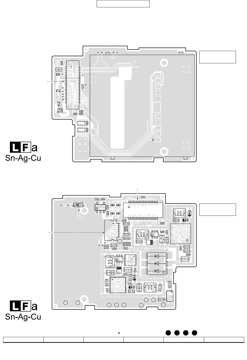
902SH
5 – 26
CONFIDENTIAL
Figure 13 WIRING SIDE P.W.BOARD (4/5)
789
10 11 12
Waveform numbers of
47
,
46
,
49
,
50
are shown on page 5-6.
TP2009TP2010
TP2012TP2013
TP2011
TP2014
TP2015
TP2017
TP2019
TP2020
TP2023
TP2022
TP2002 TP2008
TP2007
TP2006
TP2016
TP2018
TP2021
TP2000
TP2003
TP2004 TP2005
TP2024
TP2025
TP2027
TP2001
TP2026
F
FF
1
5
10
15
20
25 26
30
35
40
45
50
1
1
13
46
151015
20
21
253035
40
5
8
3
4
5
5-27 (2-C)
FROM
SD P.W.B.
CONNECT FPC
PWB-H
5-27 (6-C)
FROM
CAMERA UNIT
PWB-J
5-27 (5-G)
FROM
LCD 2000
SUB DISPLAY
SD PWB-C
(FRONT SIDE)
SD PWB-C
(REAR SIDE)
This PWB employs lead-free solder.
This PWB employs lead-free solder.
MEMORY CARD CONNTCTOR
MOBILE LIGHT
FS2000
FS2001
FS2002
CN2000
CN2001
R2000
R2001
R2002
R2003
R2004
R2006
R2012
R2017
R2022
R2023
R2024
C2045
L2001
L2002
L2003
L2004
L2005
L2006
L2007
L2008
LED2005
LED2006
CN2002
CN2003
C2000
C2001
C2003
C2004
Q2002
C2006
C2007
C2008
Q2005
C2009
C2010
C2011
C2012
C2013
C2014
C2015
C2016
C2017
C2018
C2019
C2020
C2021
C2022
C2023
D2000
C2024
D2001
C2025
D2002
C2026
D2003
C2027
D2004
C2028
D2005
C2029
R2005
R2008
IC2001
R2009
C2031
IC2002
IC2003
IC2004
IC2005
R2010
R2011
R2013
R2014
R2015
R2016
R2018
R2019
R2020
R2021
C2046
C2047
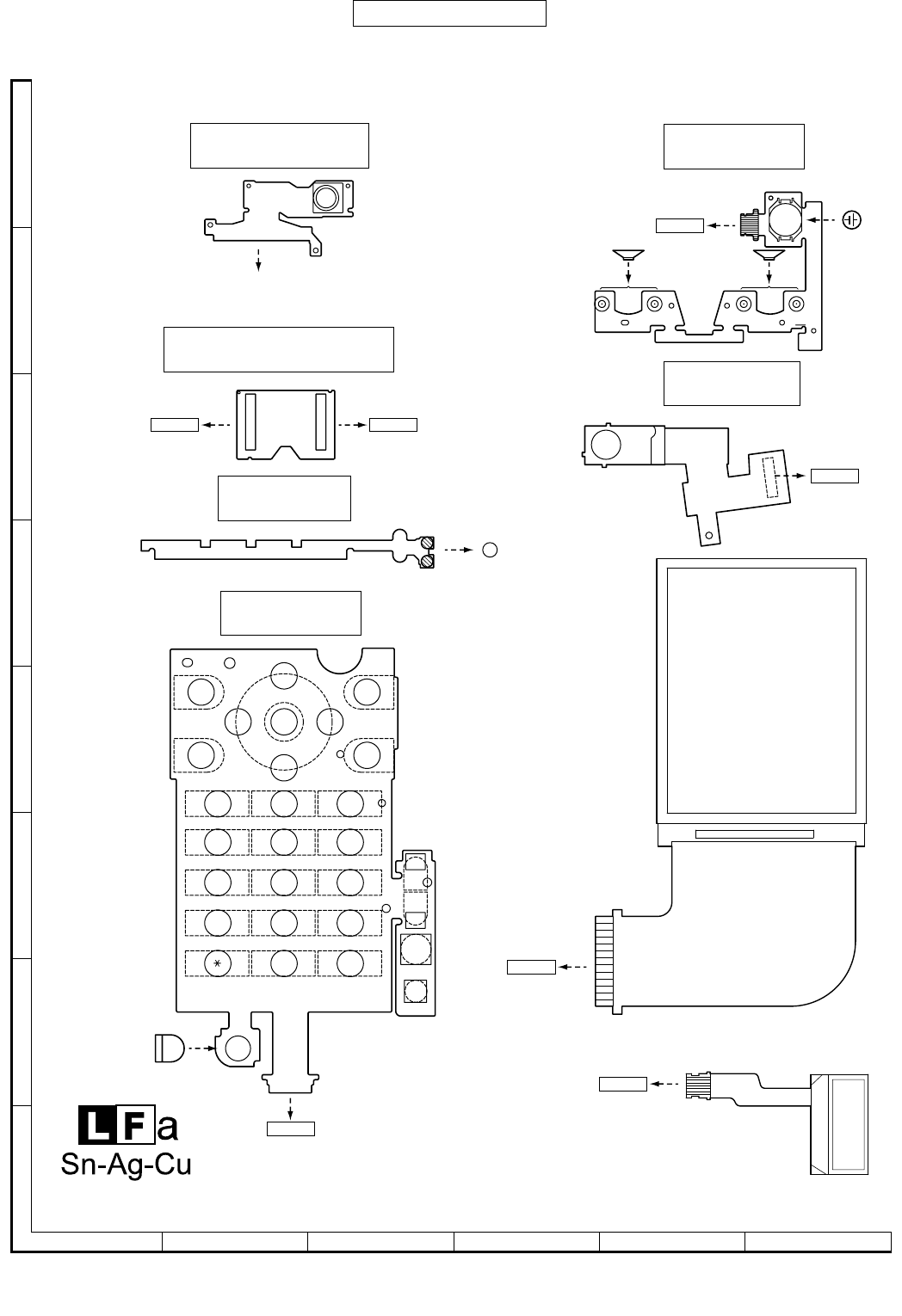
902SH
5 – 27
CONFIDENTIAL
Figure 14 WIRING SIDE P.W.BOARD (5/5)
A
B
C
D
E
F
G
H
12345 6
LCD2000
LCD3000
MIC201
SP2000
BAT1200
LED FPC UNIT
PWB-F
SD P.W.B. CONNECT FPC
PWB-H
SUB CAMERA UNIT
PWB-D
SPEAKER FPC
PWB-G
CAMERA UNIT
PWB-J
SUB DISPLAY
MAIN DISPLAY
CN2003
CN3000
A
To DISPLAY PWB-B
(REAR SIDE)
5-25 (3-E)
5-26 (10-E)
To SD PWB-C
(REAR SIDE)
SP2001
STEREO SPEAKER
STEREO SPEAKER
KEY FPC UNIT
PWB-E
CN1500
SOLDER
CN2002
To MAIN PWB-A
(REAR SIDE)
5-20 (11-B)
CN1000
5-19 (4-H)
To MAIN PWB-A
(FRONT SIDE)
MICROPHONE
CN2000
To SD PWB-C
(FRONT SIDE)
5-26 (8-B)
5-25 (5-E)
To DISPLAY PWB-B
(REAR SIDE)
5-26 (9-F)
To SD PWB-C
(REAR SIDE)
SIDE KEYS
5-25 (2-F)
To DISPLAY PWB-B
(REAR SIDE)
CN3003
5-25 (5-G)
To DISPLAY PWB-B
(REAR SIDE)
BACK-UP
BATTERY
These PWBs emplo
y
s lead-free solder.
LEFT
SOFT
SEND/
REDIAL
SHORTCUT CLEAR/BACK MULTIMEDIA
**
**
**
**
RIGHT
SOFT
CENTRE
123
456
789
0#
END/
POWER

902SH
6 – 1
CONFIDENTIAL
Phone902SHService ManualService ManualMarketE
CHAPTER 6. OTHERS
[1] Function table of IC
IC100 (OM5952AET): RECEIVER/TRANSMISSION IC FOR GSM
Pin No. Terminal name Input/Output Description of terminal
1 RFHD Input GSM 1,900 MHz RF input
2 RFHC Input GSM 1,900 MHz RF input
3 GNDRF – Earth for RF part
4 RFLB Input GSM 900 MHz or GSM 800 MHz RF input
5 RFLA Input GSM 900 MHz or GSM 800 MHz RF input
6 VCCRF – Supply for RF part
7 QRB Output Q-channel output
8 QRA Output Q-channel output
9 IRB Output I-channel output
10 IRA Output I-channel output
11 GNDRF – Earth for RF part
12 GNDVCO – Earth for VCO part
13 RFHA Input GSM 1,800 MHz RF input
14 GND PLANE – Flex-film earth plane
15 REON Input Hardware power on for reference and bus part
16 CLK Input Serial bus clock input
17 DATA Input/Output Serial bus data input/output
18 STROBE Input Serial bus strobe input
19 GNDCVO – Earth for VCO part
20* NC – Must not be connected. Bond wire exists. (Not used)
21 RFHB Input GSM 1,800 MHz band RF input
22 TXON Input Hardware power on for transmit part
23 GNDVCO – Earth for VCO part
24* NC – Not used
25 GNDRF – Earth for RF part
26 RXON Input Hardware power on for receive part
27 GNDVCO – Earth for VCO part
28 GNDVCO – Earth for VCO part
29 TXOLB Output GSM 800/900 MHz Tx output
30 BSEL Input Hardware band select control input
31 GNDVCO – Earth for VCO part
32 GNDVCO – Earth for VCO part
33 TXOLA Output GSM 800/900 MHz Tx output
34 PCTL Output Tx power control output
35 GNDVAR – Earth for varactors
36 VCCVCO Input Supply for VCO part
37 VCCBUF Input Supply for Tx input part
38 GNDBUF Input Earth for Tx input part
39 GND PLANE – Connected to flex film earth plane
40* PS – Test output (Not used)
41 GNDPLL – Earth for prescaler, phase detector and XO
42* XOOLA Output XO output (Not used)
43 GNDPLL – Earth for prescaler, phase detector and XO
44 VTUNE Input Tuning input for VCOs
45 TXOHB Output GSM 1,800/1,900 MHz Tx output
46 PHDOUT Output Phase detector output
47 TXOHA Output GSM 1,800/1,900 MHz Tx output
48* NC – Not used
49 MODA Output Prescaler modulus control output
50 MODB Output Prescaler modulus control output
51 MODC Output Prescaler modulus control output
52 MODD Output Prescaler modulus control output
53 VCCPLL Input Supply for prescaler, phase detector and XO
54 XOOB Input XO input A
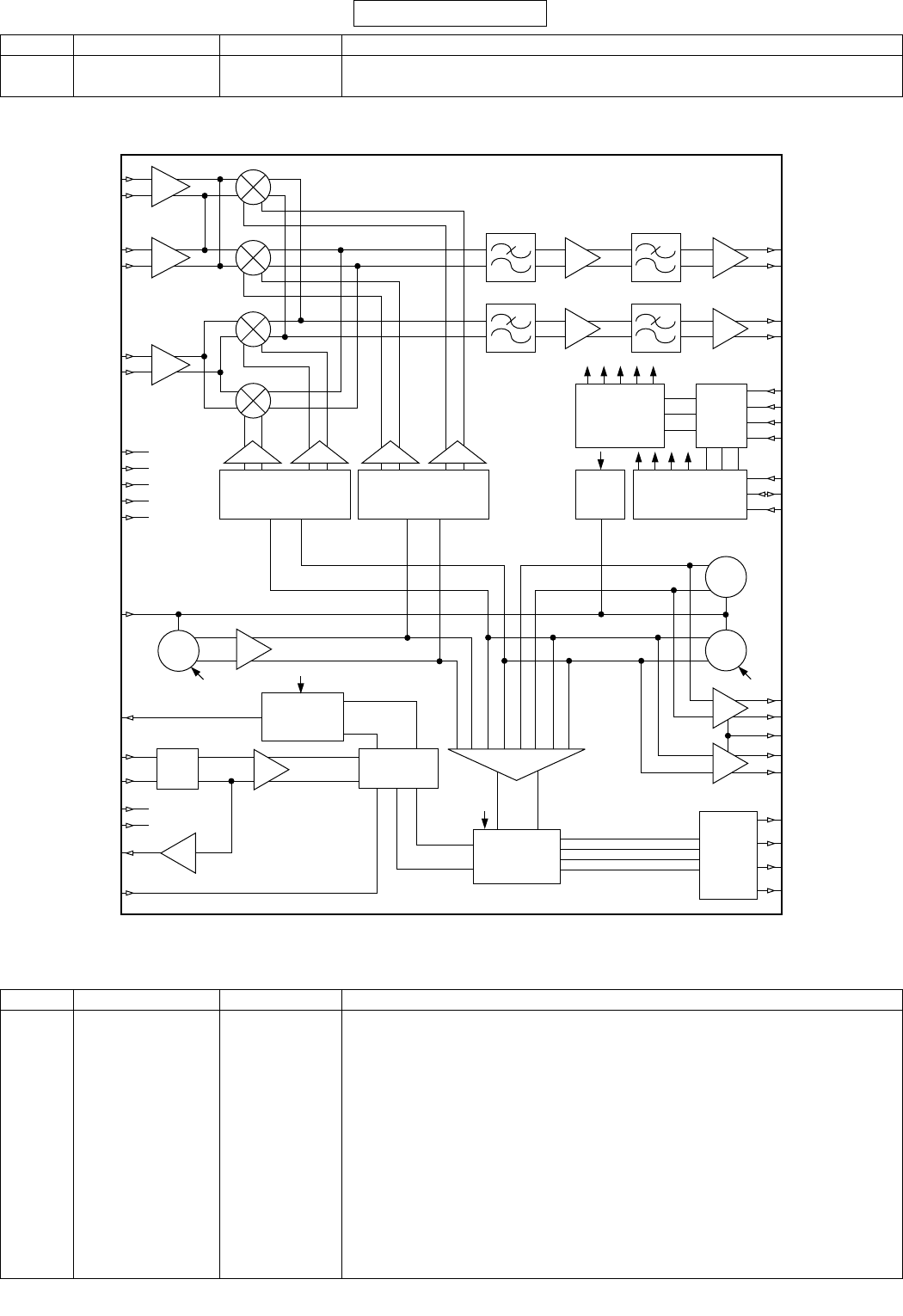
902SH
6 – 2
CONFIDENTIAL
In this unit, the terminal with asterisk mark (*) is (open) terminal which is not connected to the outside.
IC101 (AB1011): GSM CODEC
55 XOOC Input XO input B
56* NC – Not used
Pin No. Terminal name Input/Output Description of terminal
1 VSS – Earth (substrate)
2VDD – VCC
3* DAC03 – Internally connected, high impedance (floating) (Not used)
4 IDAT Output Output from ADC I-channel
5 QRB Input Differential input to the ADC Q-channel
6 QRA Input Differential input to the ADC Q-channel
7 IRB Input Differential input to the ADC I-channel
8 IRA Input Differential input to the ADC I-channel
9VSS – Earth
10 DEC4 – Reference de-coupling
11* DAC02 – Internally connected, high impedance (floating) (Not used)
12 RXSTR Input Power up for the ADCs
13 VDD – VCC
Pin No. Terminal name Input/Output Description of terminal
IRA
IRB
QRA
QRB
REON
TXOLA
TXOLB
PCTL
TXOHA
TXOHB
MODA
MODB
MODC
MODD
PS
XOOLA
GNDPLL
VCCPLL
XOOC
XOOB
PHDOUT
VTUNE
GNDVAR
GNDVCO
GNDBUF
VCCVCO
VCCBUF
RFLB
RFLA
RFHD
RFHC
RFHB
RFHA
RXON
TXON
CLK
DATA
STROBE
BSEL
DELAY
PHASE
DETECTOR
PHASE
DETECTOR
CHARGE
PUMP
XO
VCO
DIV
090 090
LNA
LNA
LNA
1,800 MHz
1,900 MHz
800/
900 MHz
DIV
VCO
VCO
VCO
TEST BUSINTERFACE
LOGIC
CURRENT
REGULATOR

902SH
6 – 3
CONFIDENTIAL
In this unit, the terminal with asterisk mark (*) is (open) terminal which is not connected to the outside.
14* GPA1 – Internally connected, high impedance (floating) (Not used)
15 VDD – VCC
16* GPA0 – Internally connected, high impedance (floating) (Not used)
17 DACDAT – Internally connected to earth (pull-down)
18 DACCLK – Internally connected to earth (pull-down)
19* DAC01 – Internally connected, high impedance (floating) (Not used)
20 VSS – Earth
21 DCLK Output Output clock from ADCs
22* GPA2 – Internally connected, high impedance (floating) (Not used)
23* GPA3 – Internally connected, high impedance (floating) (Not used)
24* GPA4 – Internally connected, high impedance (floating) (Not used)
25 I2CCLK Input Input clock of I2C bus
26 RESETB Input Power reset to the AB1011
27 I2CDAT Input Bi-directional I2C data
28 DACSTR – Internally connected to earth (pull-down)
29 QDAT Output Output from ADC Q-channel
30* GPA5 – Internally connected, high impedance (floating) (Not used)
31* GPA7 – Internally connected, high impedance (floating) (Not used)
32* GPA6 – Internally connected, high impedance (floating) (Not used)
33 DEC5 – Reference de-coupling
34 DEC1 – Reference de-coupling
35 REXT – Reference resistance
36* AUXI1 – Internally connected, high impedance (floating) (Not used)
37* GPCLK – Internally connected, high impedance (floating) (Not used)
38* GPDAT – Internally connected, high impedance (floating) (Not used)
39 ADSTR – Internally connected to earth (pull-down)
40VSS – Earth
41AVDD – VCC
42* CCO – Internally connected, high impedance (floating) (Not used)
43* MICIP – Internally connected, high impedance (floating) (Not used)
44 VSS – Earth
45VDD – VCC
46 PCMCLK – Internally connected to earth (pull-down)
47VSS – Earth
48VDD – VCC
49* MICIN – Internally connected, high impedance (floating) (Not used)
50* NC – Not used
51 VSS – Earth
52 VSS – Earth
53* BEARP – Internally connected, high impedance (floating) (Not used)
54 PCMSYN – Internally connected to earth (pull-down)
55* PCMUL – Internally connected, high impedance (floating) (Not used)
56 MCLK (SYSCLK2) Input System clock input
57* NC – Not used
58 DEC2 – Reference de-coupling
59 DEC3 – Reference de-coupling
60* AUXO2 – Internally connected, high impedance (floating) (Not used)
61* BEARN – Internally connected, high impedance (floating) (Not used)
62 VDD – VCC
63 PCMDL – Internally connected to earth (pull-down)
64 VSS – Earth
Pin No. Terminal name Input/Output Description of terminal
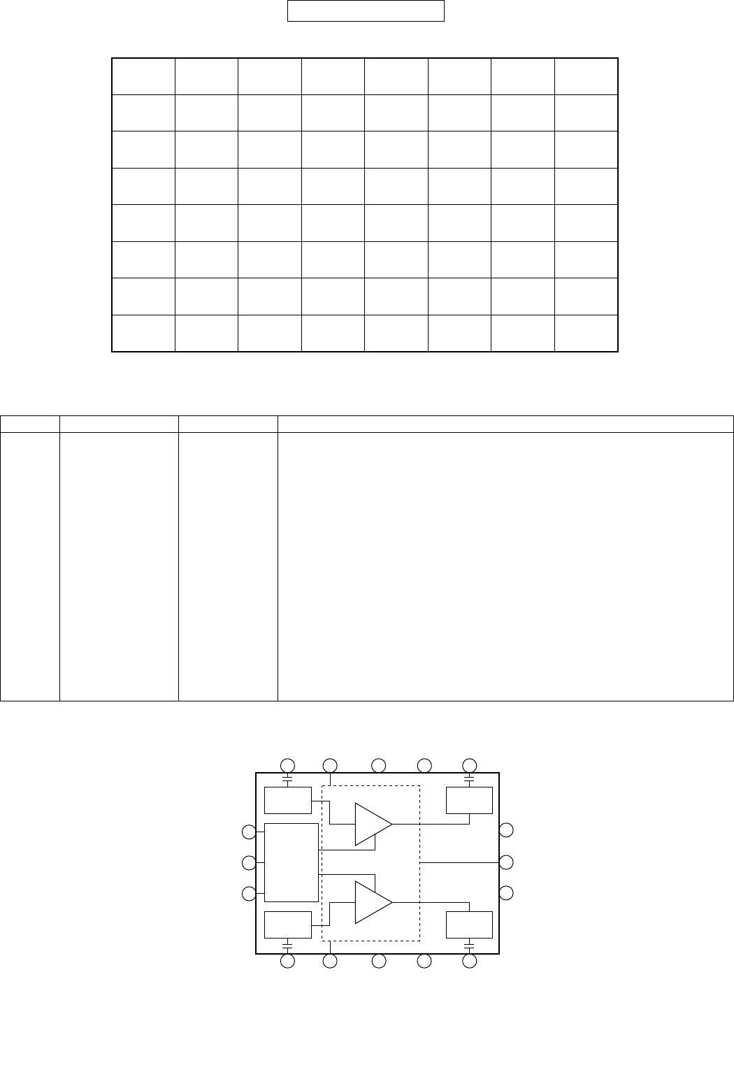
902SH
6 – 4
CONFIDENTIAL
IC300 RH-IXA038AFZZL (CX77313): POWER AMP. MODULE (FOR GSM)
Pin No. Terminal name Input/Output Description of terminal
1 DCS/PCS IN Input RF input 1,710 to 1,910 MHz
2 VAPC Input Power control bias voltage
3 VSUPPLY – DC supply to CMOS bias controller
4 BS Input Band select
5 GSM IN Input RF input 824 to 915 MHz
6 VCC – VCC (to GSM 1st stage and DCS 1st stage)
7 GND – RF and DC earth
8 GND – RF and DC earth
9 GSM OUT Output RF output 824 to 915 MHz
10 GND – RF and DC earth
11 VCC – VCC (to GSM and DCS final stages)
12 GND – RF and DC earth
13 DCS/PCS OUT Output RF output 1,710 to 1,910 MHz
14 GND – RF and DC earth
15 GND – RF and DC earth
16 VCC – VCC (to DCS 2nd stage)
A8
IRA
A7
IRB
A6
QRA
A5
QRB
A4
IDAT
A3
DAC03
A2
VDD
A1
VSS
B8
GPA0
B7
VDD
B6
GPA1
B5
VDD
B4
RXSTR
B3
DAC02
B2
DEC4
B1
VSS
C8
GPA4
C7
GPA3
C6
GPA2
C5
DCLK
C4
VSS
C3
DAC01
C2
DACCLK
C1
DACDAT
D8
GPA6
D7
GPA7
D6
GPA5
D5
QDAT
D4
DACSTR
D3
I2CDAT
D2
RESETB
D1
I2CCLK
E8
VSS
E7
ADSTR
E6
GPDAT
E5
GPCLK
E4
AUXI1
E3
REXT
E2
DEC1
E1
DEC5
F8
VDD
F7
VSS
F6
PCMCLK
F5
VDD
F4
VSS
F3
MICIP
F2
CCO
F1
AVDD
G8
MCLK
G7
PCMUL
G6
PCMSYN
G5
BEARP
G4
VSS
G3
VSS
G2
NC
G1
MICIN
H8
VSS
H7
PCMDL
H6
VDD
H5
BEARN
H4
AUXO2
H3
DEC3
H2
DEC2
H1
NC
2
1 16 15 14 13
12
11
10
98765
VAPC
DCS/
PCS IN VCC GND GND
GND
VCC
GND
GSM OUTGNDGNDVCCGSM IN
DCS/
PCS OUT
3
VSUPPLY
4
BS
HBT
Match Match
Match
CMOS
Bias
Controller
Match

902SH
6 – 5
CONFIDENTIAL
IC400 (OM5954ET): RECEIVER IC FOR W-CDMA
Pin No. Terminal name Input/Output Description of terminal
1 IFOUTA Output IF output A (balanced)
2 GNDMIX – Earth for RF mixer
3 VCCIF – Supply for IF
4 IFINA Input IF input A (balanced)
5 IFINB Input IF input B (balanced)
6 VCCLF – Supply for baseband part
7 QRA Output Q-channel output
8 QRB Output Q-channel output
9 IRA Output I-channel output
10 IRB Output I-channel output
11 IFOUTB Output IF output B (balanced)
12 VCCREF – Supply for reference
13 VCCMIX – Supply for RF mixer
14 GNDIF – Earth for IF mixer
15 CDQ – External capacitor connection for baseband DC compensation loop (Q-channel)
16 CDI – External capacitor connection for baseband DC compensation loop (I-channel)
17 GNDLF – Earth for baseband part
18 MCLK Output XO master clock output
19 XOOA Output XO output A (balanced)
20 XOIA Input XO input A (balanced)
21 MIXINA Input RF mixer input A (balanced)
22 DATA Input Serial bus data input
23 XOOB Output XO output B (balanced)
24 XOIB Input XO input B (balanced)
25 MIXINB Input RF mixer input B (balanced)
26 CLK Input Serial bus clock input
27 GNDREF – Earth for reference
28 VCCBUS – Supply for data bus
29 GNDBIAS – Earth for bias
30 STROBE Input Serial bus strobe input
31 GNDBUS – Earth for data bus
32 IFLOA Input IFLO input A (balanced)
33 GNDEME – Earth for RF LNA
34 GLNA Output Gain control output for external RF LNA parts
35 REFON Input Hardware power on for ref.
36 IFLOB Input IFLO input B (balanced)
37 RFIN Input RF LNA input
38 XOOON Input Hardware power on for XO output
39 RXON Output Hardware power control output for external receiver parts
40 GNDPLL – Earth for PLL
41 GNDPHD – Earth for phase detector
42 GNDTUNE – Earth for varactor
43 GNDVCO – Earth for VCO
44 GNDRFLO – Earth for RFLO
45 GNDBYP – Earth for bypass RF LNA
46 RFLOOA Output RFLO output A (balanced)
47 VCCRF – Supply for RF LNA
48 INDBYP – Earth for RF LNA inductor bypass
49 RFOUT Output RF LNA output
50 VCCPLL – Supply for PLL
51 VCCPHD – Supply for phase detector
52 PHDOUT Output Phase detector output
53 VTUNE Input Tuning input for VCOs
54 VCCVCO – Supply for VCO
55 VCCRFLO – Supply for RFLO
56 RFLOOB Output RFLO output B (balanced)
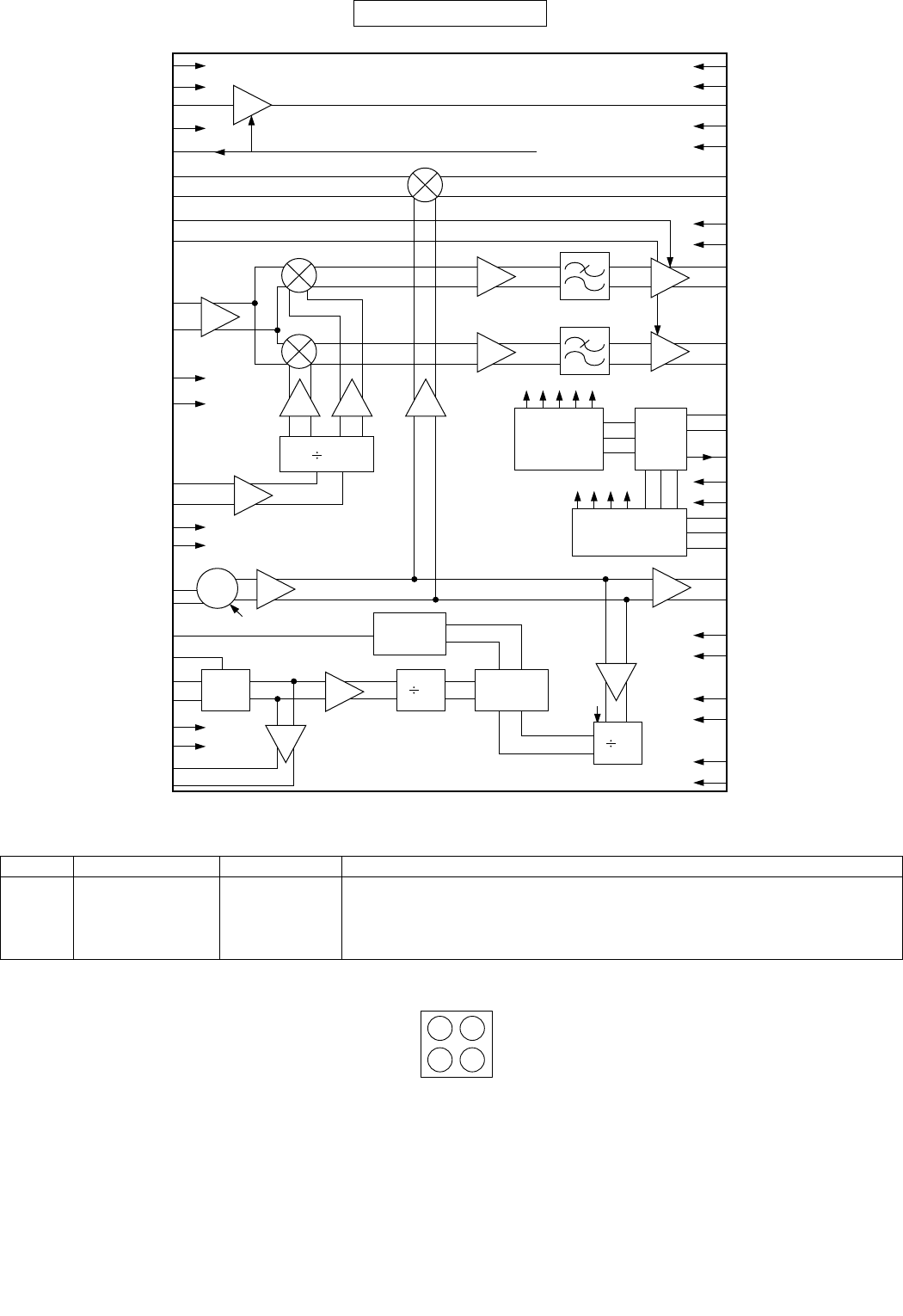
902SH
6 – 6
CONFIDENTIAL
IC501/IC1209 VHILM20SITN-1R (LM20SITLX): TEMPERATURE SENSOR
In this unit, the terminal with asterisk mark (*) is (open) terminal which is not connected to the outside.
Pin No. Terminal name Input/Output Description of terminal
1* NC – Not used
2GND – Earth
3 VO Output Output
4 V+ – Power supply
From Bus
INDBYP
GNDBYP
RFOUT
VCCMIX
GNDMIX
IFOUTA
IFOUTB
VCCLF
GNDLF
IRA
IRB
QRA
REFON
RXON
VCCBUS
GNDBUS
CLK
DATA
STROBE
RFLOOA
RFLOOB
VCCRFLO
GNDRFLO
VCCPHD
GNDPHD
VCCPLL
GNDPLL
XOOB
XOOA
GNDREF
VCCREF
XOIB
XOIA
MCLK
PHDOUT
GNDTUNE
GNDVCO
VCCVCO
IFLOB
IFLOA
GNDIF
VCCIF
IFINB
IFINA
CDQ
CDI
MIXINB
MIXINA
GLNA
GNDEME
RFIN
GNDBIAS
VCCRF
VTUNE
XOOON
QRB
LNA
LNA
VGA
VGA
VCO
CHARGE
PUMP
PHDR
N
XO
LOGIC
CURR. REG.
2,140 MHz
190 MHz
4
090
BUS
INTERFACE
4 3
2 1
V+
GND
VO
NC
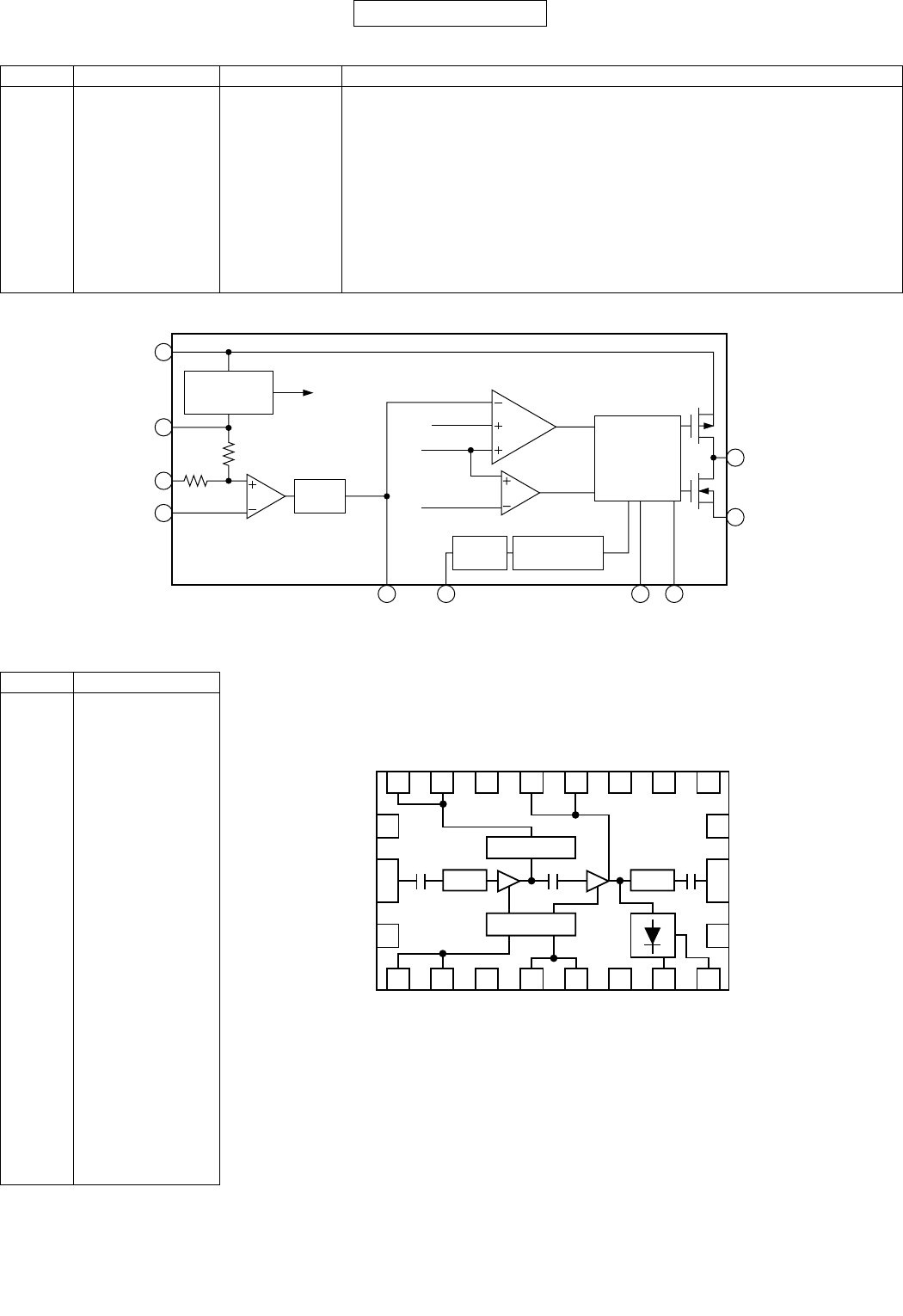
902SH
6 – 7
CONFIDENTIAL
IC620 VHIM1820XCP-1L (MAX1820XEBC): DCDC
IC630 RH-IX3045AFZZL (RF9266): W-CDMA POWER AMP.
Pin No. Terminal name Input/Output Description of terminal
1 /SKIP Input PWM/Skip-mode input
2 COMP – Compensation
3 OUT Input Output voltage sense input
4 REF Input External reference input
5GND – Earth
6 PGND – Power earth
7 LX Output Inductor connection
8 BATT Input Supply voltage input
9 /SHDN Input Active-low, shutdown control input
10 SYNC Input Clock synchronisation input
Pin No. Terminal name
1 V CTRL (VREG)
2 V CTRL (VREG)
3GND
4 VCC_BIAS
5 VCC_BIAS
6GND
7 VCC DET
8 V DETECT
9GND
10 RF OUT
11 GND
12 GND
13 GND
14 GND
15 VCC2
16 VCC2
17 GND
18 VCC1
19 VCC1
20 GND
21 RF IN
22 GND
Pkg
Base
GND
BATT
LX
PGND
GND
OUT
REF
COMP SYNC /SKIP /SHDN
TO
IC BIAS
VOLTAGE
REFERENCE
CLAMP
TRANSIMPEDANCE
ERROR AMP
ERROR
SIGNAL
SLOPE COMP
CURRENT
SENSE
PWM
COMPARATOR
SKIP
COMPARATOR
PWM
CONTROL
AND
SKIP LOGIC
SKIP
THRESHOLD
1 MHz
OSCILLATOR
+13 OR
+18
1.25 V
0.45 V TO 2.15 V
8
5
3
4
2 1 9
6
7
10
19 18 1617 15 14 13 12
1 2 43 5 6 7 8
20
21
22
11
10
9
Interstage MN
IMN OMN
Bias Control Power
Detector
Network
VCC1
VCC1
VCC2
VCC2
GND
GND
GND
GND
GND
GND
GND
RF IN
GND
GND
RF OUT
GND
VCTRL
VCTRL
VCC BIAS
VCC BIAS
VCC DET
VDET

902SH
6 – 8
CONFIDENTIAL
IC700 (OM5955ET): W-CDMA TRANSMITTER IC
In this unit, the terminal with asterisk mark (*) is (open) terminal which is not connected to the outside.
Pin No. Terminal name Input/Output Description of terminal
1 QINBAR Input Negative quadrature phase input signal
2 QIN Input Positive quadrature phase input signal
3 IINBAR Input Negative in phase input signal
4 IIN Input Positive in phase input signal
5 VCCBB – VCC for baseband blocks
6 VCCIFPHD – VCC for IF PLL charge pump
7 PHDIFOUT Output IF PLL charge pump output
8 VCCIFPLL – VCC for IF PLL
9 GNDIFVCO – Earth for IF VCO
10 VCCIFVCO – VCC for IF VCO
11 XOOB Input Reference frequency input (13 MHz)
12 VTUNEIF Input IF VCO voltage tuning input
13 XOOC (XOOA) Input Reference frequency input (13 MHz)
14 GNDBB – Earth for baseband blocks
15 CLK Input Serial bus clock input
16 GNDIFPHD – Earth for IF PLL charge pump
17 GNDIFPLL – Earth for IF PLL
18 WON Output Logic output to control aerial switch
19 GNDIFVCO – Earth for IF VCO
20 GNDTUIF – Earth for IF VCO varactor
21 VCCBUS – VCC for bus and logic blocks
22 GNDBUS – Earth for bus and logic blocks
23 GNDRFPHD – Earth for RF PHD
24 GNDIFVCO – Earth for IF VCO
25 IFLO Output Positive IF LO frequency output
26 DATA Input Serial bus data input
27 TXON Output Hard wired TX ON logic output
28 VCCRFPHD – VCC for RF PHD
29 IFLOBAR Input Negative IF LO frequency input
30 GNDIFLO – Earth for IF LO
31 GNDRFPLL – Earth for RF VCO
32* PHDRFOUT Output RF PLL charge pump output (Not used)
33 VCCIFLO – VCC for IF LO
34 GNDRFLO – Earth for RF LO
35 STROBE Input Serial bus strobe input
36 VCCRFPLL – VCC for RF VCO
37 RFLO Input Positive RF mixer LO input
38 GNDRFLO – Earth for RF LO
39 GNDRF – Earth for RF parts
40 GNDRF – Earth for RF parts
41 GNDRF – Earth for RF parts
42 GNDIF – Earth for intermediate frequency parts
43 GNDRFVCO – Earth for RF VCO
44 VCCRFVCO – VCC for RF VCO
45 RFLOBAR Input Negative RF mixer LO input
46 GNDTURF – Earth for RF VCO varactor
47 VCCRF – VCC for RF parts
48 OUT Output Positive RF frequency output
49 OUTBAR Output Negative RF frequency output
50 GNDRF – Earth for RF parts
51 VCCRF – VCC for RF parts
52 VCCRF – VCC for RF parts
53 VCCIF – VCC for intermediate frequency parts
54 IFBP – IF filter tank port
55 IFBPBAR – IF filter negative tank port
56* VTUNERF Input RF VCO voltage tuning input (Not used)
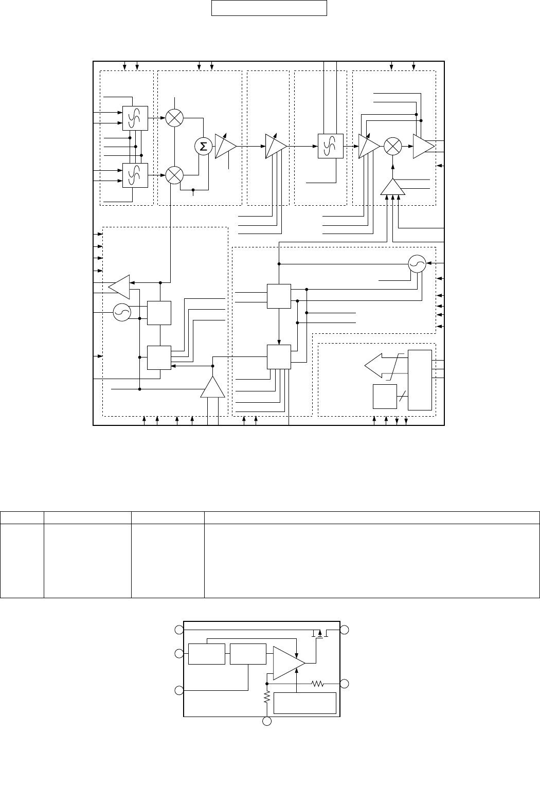
902SH
6 – 9
CONFIDENTIAL
IC800 VHI3981D28N-1R (LP3981ILD): 2.8 V REGULATOR
Pin No. Terminal name Input/Output Description of terminal
1 VOUT Output Output Voltage of the LDO
2 VIN Input Input Voltage of the LDO
3 VOUT-SENSE Output Output. Voltage Sense Pin
4 GND – Common Earth
5 BYPASS – Optional bypass capacitor for noise reduction
6 VEN Input Enable Input Logic, Enable High
IIN
TXON
TXON
TXON
TXON
VGAGAIN
QVGAGAIN
TXON
IQGAIN
VGA
TXON
LPO
RECDCI
Reconstruction
filters
IQ-modulator
LPBW
RECDCQ
TBIFS1
IF PLL
RFRDIV
RFLOON
SERIAL BUS
LOINTEXT
RFIPHO
TBRFS1
TBRFS0
TBRFVCO
RFVCOC
RF PLL
BUFFGAIN
BUFFGAIN2
GAINMETH
IF BP
Filter
RF-mixer and RF buffer
RFBIAS
RFNDIV
TBIFS0
TBIFVCO
IFLOON
IINBER
QIN
QINBAR
VCCIFLO
GNDIFLO
VCCIFVCO
GNDIFVCO
IFLO
IFLOBAR
VTUNEIF
GNDTUIF
GNDRFPLL
GNDBUS
VCCBUS
GNDRFPHD
VCCIFPHD
GNDIFPHD
GNDIFPLL
GNDBB
VCCBB
VCCIF
IFBPBAR
IFBP
GNDRF
VCCRF
GNDIF
VCCIFPLL
VCCRFPHD
PHDRFOUT
GNDTURF
XOOC (XOOA)
XOOB
TXON
WON
VCCRFPLL
GNDRFVCO
VCCRFVCO
GNDRFLO
OUTBAR
RFLOON
LOINTEXT
OUT
RFLOBAR
RFLO
VTUNERF
PHDIFOUT
CLK
DATA
STROBE
PHD
DIV
DIV
PHD
Logic
Serial
Bus
VIN
VEN
BYPASS
GND
VOUT-SENSE
VOUT
R2
Vreference
1.23 V
Fast Turn
On Circuit
Over Current &
Thermal Protection
2
6
5
4
3
1

902SH
6 – 10
CONFIDENTIAL
IC1001 VHIBGB202++-1L (BGB202): BLUETOOTH
Pin No. Terminal name Input/Output Description of terminal
1GND – Earth
2 ANT Input/Output Aerial input/output
3GND – Earth
4 GND – Earth
5GND – Earth
6GND – Earth
7GND – Earth
8GND – Earth
9GND – Earth
10 GND – Earth
11 GND – Earth
12 GND – Earth
13 GND – Earth
14 GND – Earth
15 GP_CLK Output General purpose clock
16 VBAT Input Battery measurement voltage input
17 VANLI Input 8-bit A/D input
18 XTAL2_LPO Output Low power crystal oscillator
19 XTAL1_LPO Input Low power crystal oscillator
20 GPIO[1] Input/Output I2C_SDA
21 GPIO[0] Input/Output I2C_SCL
22 VANLO Output Analogue voltage source output
23 GPIO[13] Input/Output General purpose I/O 13
24 GPIO[11] Input/Output General purpose I/O 11
25 GPIO[10] Input/Output General purpose I/O 10
26 1.8 V DECOUP – VDD18 decoupling
27 POR_
DISABLE
Input Power-On Reset disable input
28 XTAL2_SYS Output System clock crystal oscillator
29 XTAL1_SYS Input System clock crystal oscillator
30 REF_CLK Output Synthesiser reference frequency
31 GPIO[12] Input/Output General purpose I/O 12
32 GPIO[14] Input/Output General purpose I/O 14
33 GPIO[7]
FSC_IP
Input General purpose I/O 7
PCM/IOM frame sync
34 GPIO[9]
DB_IP
Input/Output General purpose I/O 9
Bidirectional PCM/IOM data line B (default: input)
35 GPIO[6]
DA_IP
Input/Output General purpose I/O 6
Bidirectional PCM/IOM data line A (default: output)
36 GPIO[8]
DCLK_IP
Input General purpose I/O 8
PCM/IOM data clock
37 VDD18 Input 1.8 V I/O supply voltage
38 VDD_IOV Input Variable I/O supply voltage
39 VDDIORF Input RF supply voltage
40 VREG18 Output 1.8 V regulated output voltage
41 GPIO[3]
RTS_UART
Input General purpose I/O 3
UART request-to-send input
42 GPIO[5]
RXD_UART
Input General purpose I/O 5
UART receive input
43GPIO[4]
TXD_UART
Output General purpose I/O 4
UART transmit output
44 GPIO[2]
CTS_UART
Output General purpose I/O 2
UART clear-to-send output
45 RESET_N Input Reset input (active LOW)
46 1.8 V DECOUP – VDD18 decoupling
47 TMS_JTAG Input JTAG test mode select
48 TDO_JTAG Output JTAG test data output
49 TDI_JTAG Input JTAG test data input
50 TCK_JTAG Input JTAG test clock

902SH
6 – 11
CONFIDENTIAL
IC1100 (LHF65NZ1): FLASH MEMORY 1
51 GND – Earth
52 GND – Earth
Pin No. Terminal name Input/Output Description of terminal
1* NC – Not used
2* NC – Not used
3* NC – Not used
4* NC – Not used
5 A4 Input Address input
6 A18 Input Address input
7 A19 Input Address input
8VSS – Earth
9 F1-VCC – Power supply (flash)
10 F2-VCC – Power supply (flash)
11 A21 Input Address input
12 A11 Input Address input
13 A5 Input Address input
14* /R-LB Input (Not used)
15 A23 Input Address input (flash 1, 3)
16 VSS – Earth
17* S-CS2 Input (Not used)
18 CLK Input Clock input
19 A22 Input Address input
20 A12 Input Address input
21 A3 Input Address input
22 A17 Input Address input
23 GND – Earth
24 F-VPP Input Supply voltage detection terminal
25* /R-/WE Input Write enable input (Not used)
26* /P1-CS Input (Not used)
27 A9 Input Address input
28 A13 Input Address input
29 A2 Input Address input
30 A7 Input Address input
31 GND – Earth
32 F-/WP Input Write protect input
33 /ADV Input Address valid input
34 A20 Input Address input
35 A10 Input Address input
36 A15 Input Address input
37 A1 Input Address input
38 A6 Input Address input
39* /R-UB Input (Not used)
40 F-/RST Input Reset input (flash)
41 F-/WE Input Write enable input
42 A8 Input Address input
43 A14 Input Address input
44 A16 Input Address input
45 A0 Input Address input
46 DQ8 Input/Output Data input/output
47 DQ2 Input/Output Data input/output
48 DQ10 Input/Output Data input/output
49 DQ5 Input/Output Data input/output
50 DQ13 Input/Output Data input/output
51 WAIT Output Wait output
52 F2-/CE Input Chip enable input (flash)
53* /R-OE Input Output enable input (flash) (Not used)
Pin No. Terminal name Input/Output Description of terminal

902SH
6 – 12
CONFIDENTIAL
In this unit, the terminal with asterisk mark (*) is (open) terminal which is not connected to the outside.
54 DQ0 Input/Output Data input/output
55 DQ1 Input/Output Data input/output
56 DQ3 Input/Output Data input/output
57 DQ12 Input/Output Data input/output
58 DQ14 Input/Output Data input/output
59 DQ7 Input/Output Data input/output
60 F2-/OE Input Output enable input (flash)
61* /S-CS1 Input (Not used)
62 F1-/OE Input Output enable input (flash)
63 DQ9 Input/Output Data input/output
64 DQ11 Input/Output Data input/output
65 DQ4 Input/Output Data input/output
66 DQ6 Input/Output Data input/output
67 DQ15 Input/Output Data input/output
68 VCCQ – Input/output supply
69 F1-/CE Input Chip enable input (flash)
70* /P2-CS Input (Not used)
71 F3-/CE Input Chip enable input (flash)
72* S-VCC – Power supply (Not used)
73* P-VCC – Power supply (Not used)
74 F2-VCC – Power supply (flash)
75 VCCQ – Input/output supply
76* P-MODE/PCRE Input (Not used)
77 VSS – Earth
78 VSS – Earth
79 VCCQ – Input/output supply
80 F1-VCC – Power supply (flash)
81 VSS – Earth
82 VSS – Earth
83 VSS – Earth
84 VSS – Earth
85* NC – Not used
86* NC – Not used
87* NC – Not used
88* NC – Not used
Pin No. Terminal name Input/Output Description of terminal
A23
WAIT
F1:256M (x16) bit
Flash memory
F2:128M (x16) bit
Flash memory
F3:256M (x16) bit
Flash memory
F-VPP, F1-VCC, F2-VCC
A0~A22
F1-/CE
F1-/OE
F-/WE, F-/WP, F-/RST
/ADV, CLK
F2-/CE
F2-/OE, F3-/OE
F3-/CE
DQ0~DQ15
GND

902SH
6 – 13
CONFIDENTIAL
IC1101 (MB82R6A5C): FLASH MEMORY 2
Pin No. Terminal name Input/Output Description of terminal
1* NC – Not used
2* NC – Not used
3* NC – Not used
4* NC – Not used
5* NC – Not used
6* NC – Not used
7* NC – Not used
8* NC – Not used
9* NC – Not used
10* NC – Not used
11* NC – Not used
12* NC – Not used
13* NC – Not used
14* NC – Not used
15* NC – Not used
16 A7 Input Address input
17 /LB Input Least significant byte control (low active)
18* /ADV Input FCRAM matched address input (low active) (Not used)
19 WE Input Write enable (low active)
20 A8 Input Address input
21 A11 Input Address input
22* NC – Not used
23* NC – Not used
24* NC – Not used
25 A3 Input Address input
26 A6 Input Address input
27 /UB Input Most significant byte control (low active)
28 CE2f_1 Input FCRAM chip enable (high active)
29 CE2f_2 Input FCRAM chip enable (high active)
30 A19 Input Address input (FCRAM only)
31 A12 Input Address input
32 A15 Input Address input
33* NC – Not used
34* NC – Not used
35 A2 Input Address input
36 A5 Input Address input
37 A18 Input Address input
38* /WAIT Output FCRAM wait output (high active) (Not used)
39 A20 Input Address input (FCRAM only)
40 A9 Input Address input
41 A13 Input Address input
42 A21 Input Address input (FCRAM only)
43* NC – Not used
44* NC – Not used
45 A1 Input Address input
46 A4 Input Address input
47 A17 Input Address input
48 /CE1s Input SRAM chip enable (low active)
49* NC – Not used
50 A10 Input Address input
51 A14 Input Address input
52 A22 Input Address input (FCRAM only)
53* NC – Not used
54* NC – Not used
55 A0 Input Address input
56 VSS – Earth
57 DQ2 Input/Output Least significant byte data input/output
58 VDDS – SRAM supply voltage

902SH
6 – 14
CONFIDENTIAL
In this unit, the terminal with asterisk mark (*) is (open) terminal which is not connected to the outside.
59 CE2s Input SRAM chip enable (high active)
60 DQ7 Input/Output Least significant byte data input/output
61 CLK Input FCRAM clock input
62 A16 Input Address input
63* NC – Not used
64* NC – Not used
65 /CE1f_1 Input FCRAM chip enable (low active)
66 OE Input Output enable (low active)
67 DQ10 Input/Output Most significant byte data input/output
68 DQ4 Input/Output Least significant byte data input/output
69 DQ5 Input/Output Least significant byte data input/output
70 DQ14 Input/Output Most significant byte data input/output
71 DQ16 Input/Output Most significant byte data input/output
72* NC – Not used
73* NC – Not used
74* NC – Not used
75 /CE1f_2 Input FCRAM chip enable (low active)
76 DQ1 Input/Output Least significant byte data input/output
77 DQ11 Input/Output Most significant byte data input/output
78 VDDf_1 – FCRAM supply voltage
79 VDDQf_1 – FCRAM_1 input/output supply voltage
80 DQ13 Input/Output Most significant byte data input/output
81 DQ8 Input/Output Least significant byte data input/output
82 VSS – Earth (SRAM only)
83* NC – Not used
84* NC – Not used
85* NC – Not used
86 DQ9 Input/Output Most significant byte data input/output
87 DQ3 Input/Output Least significant byte data input/output
88 DQ12 Input/Output Most significant byte data input/output
89* NC – Not used
90 DQ6 Input/Output Least significant byte data input/output
91 DQ15 Input/Output Most significant byte data input/output
92* NC – Not used
93* NC – Not used
94* NC – Not used
95* NC – Not used
96* NC – Not used
97* NC – Not used
98 VDDf_2 – FCRAM supply voltage
99* NC – Not used
100* NC – Not used
101* NC – Not used
102* NC – Not used
103* NC – Not used
104* NC – Not used
105* NC – Not used
106* NC – Not used
107* NC – Not used
Pin No. Terminal name Input/Output Description of terminal
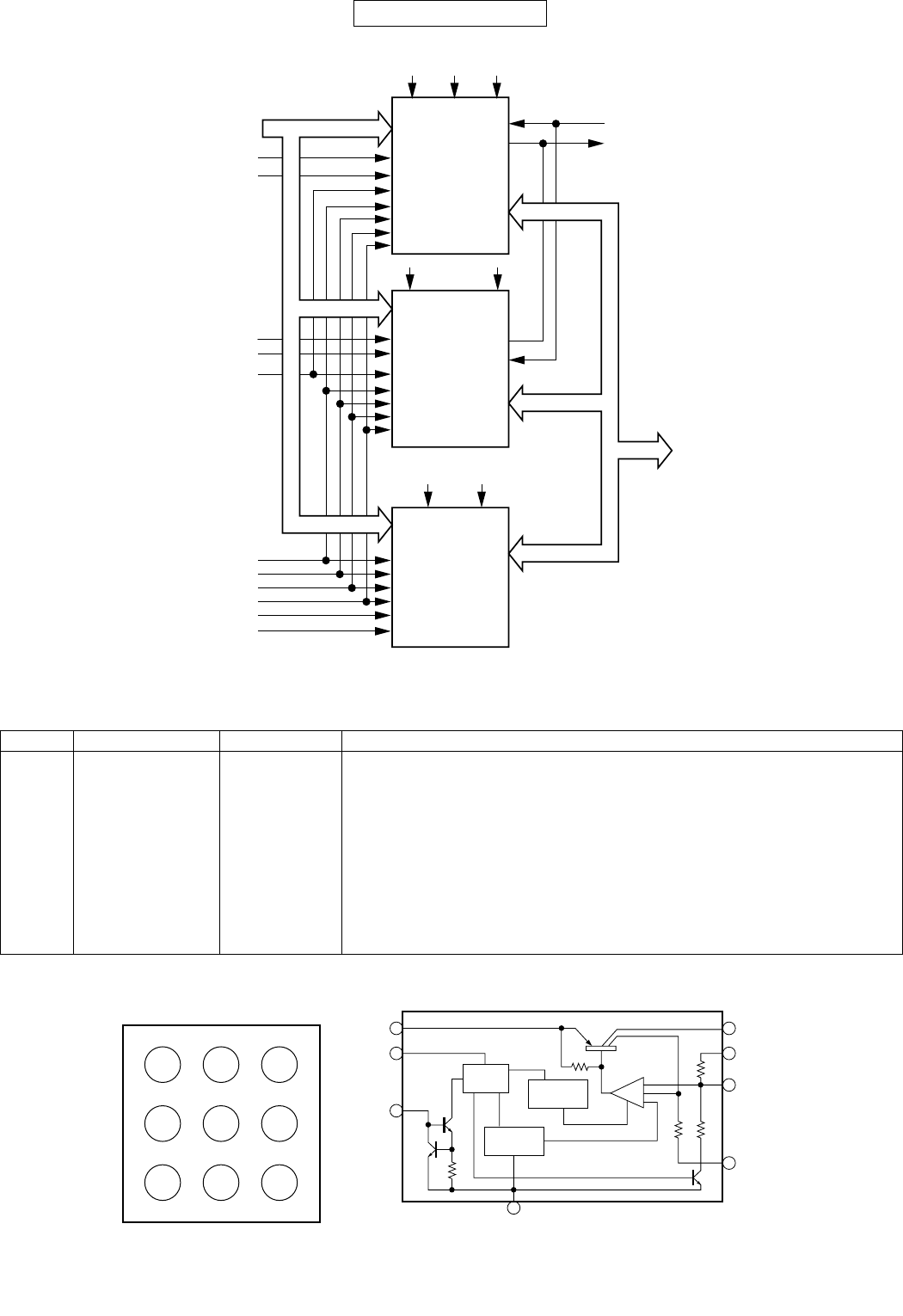
902SH
6 – 15
CONFIDENTIAL
IC1202 VHITK73840G-1L (TK73840BDB): REGULATOR
In this unit, the terminal with asterisk mark (*) is (open) terminal which is not connected to the outside.
Pin No. Terminal name Input/Output Description of terminal
1 VCONT
(ON/OFF)
Input Power control
2 BIN (PE) Input Power enable
3 VIN (Vin) Input Power supply
4 PCL (ACL) Input Current setting
5 NC (GND) – Earth
6 GND (GND) – Earth
7* VFB (Vfb) Input Not used
8 VSENSE (PC) Output Power output
9 VOUT (Vout) Output Power output
CE2s
CE1s
OE
WE
/UB
/LB
/ADV
CE2f_2
/CE1f_2
CE2f_1
/CE1f_1
CLK
/WAIT
DQ16 to DQ1
A22 to A0
A21 to A0
A18 to A0
VDDf_2
VDDS VSS
VSS
VDDf_1
128 M bit
FCRAM_1
64 M bit
FCRAM_2
8 M bit
SRAM
VDDQf_1 VSS
VCONT
VIN
Bandgap
Reference
Control
Circuit Over Heat
Protect
3
BIN 2
1
VOUT
9
VFB
7
GND
5,6
VSENSE
8
PCL
4
3
VIN 6
GND 9
VOUT
2
BIN 5
NC 8
VSENSE
1
VCONT
4
PCL 7
VFB
1
AB
TOP VIEW
C
2
3

902SH
6 – 16
CONFIDENTIAL
IC1300 VHIBU7880GU-1L (BU7880GU): EXTERNAL INTERFACE
In this unit, the terminal with asterisk mark (*) is (open) terminal which is not connected to the outside.
Pin No. Terminal name Input/Output Description of terminal
1 UART_RXD1 Output UART_RXD1 output
2 BDATA Input BDATA input
3 UART_RTS Input UART_RTS input
4 UART_TXD1 Input UART_TXD1 input
5 SCLK Input SCLK input
6 BSYNC Input BSYNC input
7* UART_RXD2 Output UART_RXD2 output (Not used)
8 BCNT Input BDATA input control
9 UART_CTS Output UART_CTS output
10 UART_TXD2 Input UART_TXD2 input
11 BSSEL Input BSYNC/SCLK switching control
12 GND – Earth
13 VBAT – Power supply for switch
14 PUEA Input PU15 control input
15* NC – Not used
16* GND – Earth (Not used)
17 UARTSEL Input UART 1 and 2 switching terminal input
18 UARTMD Input UART mode switching
19 CPU_USB_D+ Input/Output CPU_USB_D+ input/output
20 REG33 – USB power supply
21* GND – Earth (Not used)
22* GND – Earth (Not used)
23 HFMD Input Hands free mode switching
24 CPUVDD – Digital power supply
25 USBD+/RXD Input/Output USBD+/RXD switching external input/output
26 PU15 Output PMOS open drain output
27 BSYNC/SCLK/RTS Output BSYNC/SCLK/RTS switching external output
28 GND – Earth
29* RXANAIN Input Hands free receiving external input (Not used)
30 USBMD Input USB mode switching
31 CPU_USB_D– Input/Output CPU_USB_D– inupt/output
32 USBD-/TXD Input/Output USBD–/TXD switching external input/output
33 BDATA/CTS Input/Output BDATA/CTS switching external input/output
34* TXANAIN Input Hands free sending input (Not used)
35* RXANAOUT Output Hands free receiving output (Not used)
36* TXANAOUT Output Hands free sending external output (Not used)
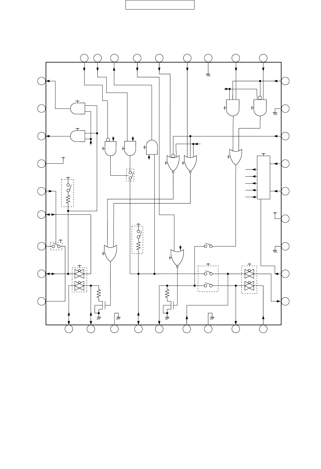
902SH
6 – 17
CONFIDENTIAL
BSSEL
11
12
17
18
23
24
22
30
36
GND
UARTSEL
UARTMD
HFMD
CPUVDD
GND
USBMD
TXANAOUT
RXANAIN
31 32 21 33 27 34 28 35 29
RXANAOUT
GND
TXANAIN
BSYNC/SCLK/RTS
BDATA/CTS
GND
USBD-/TXD
CPU_USB_D-
BCNT
65164103928
BDATA
UART_CTS
UART_RTS
UART_TXD2
UART_TXD1
GND
SCLK
BSYNC
PU15 26
25
20
19
14
13
7
1
15
USBD+/RXD
REG33
CPU_USB_D+
PUEA
VBAT
UART_RXD2
UART_RXD1
NC
MODE 0, 1, 4 : L
MODE 2, 3: H
CPUVDD
CPUVDD
CPUVDD
MODE 0, 1, 3, 4 : L
MODE 2: H
VBAT
CPUVDD
H:ON
L: OFF
VBAT
CPUVDD
MODE0,1,3,4:OFF
MODE 2: ON
10k
VBAT
MODE 0, 2, 3 : OFF
MODE 1, 4: ON
VBAT
MODE 0, 1, 2 : OFF
MODE 3, 4: ON
MODE 0, 1, 2 : ON
MODE 3, 4: OFF
VBAT
DECODER
CPUVDD
CPUVDD
MODE 0, 2, 3, 4 : OFF
MODE 1: ON
CPUVDD
CPUVDD
MODE 0, 2, 3, 4: L
MODE 1: H
MODE 0, 1, 4: L
MODE 2, 3: H
MODE 0, 1, 3, 4: H
MODE 2: L CPUVDD
CPUVDD
CPUVDD
MODE0,2,3,4:L
MODE 1: H
CPUVDD
MODE0,2,3,4:L
MODE 1: H
CPUVDD
MODE 0, 1, 4 : OFF
MODE 2, 3: ON
10k
CPUVDD
CPUVDD
MODE 0
MODE 1
MODE 2
MODE 3
MODE 4
BU7880GU
H:ON
L: OFF
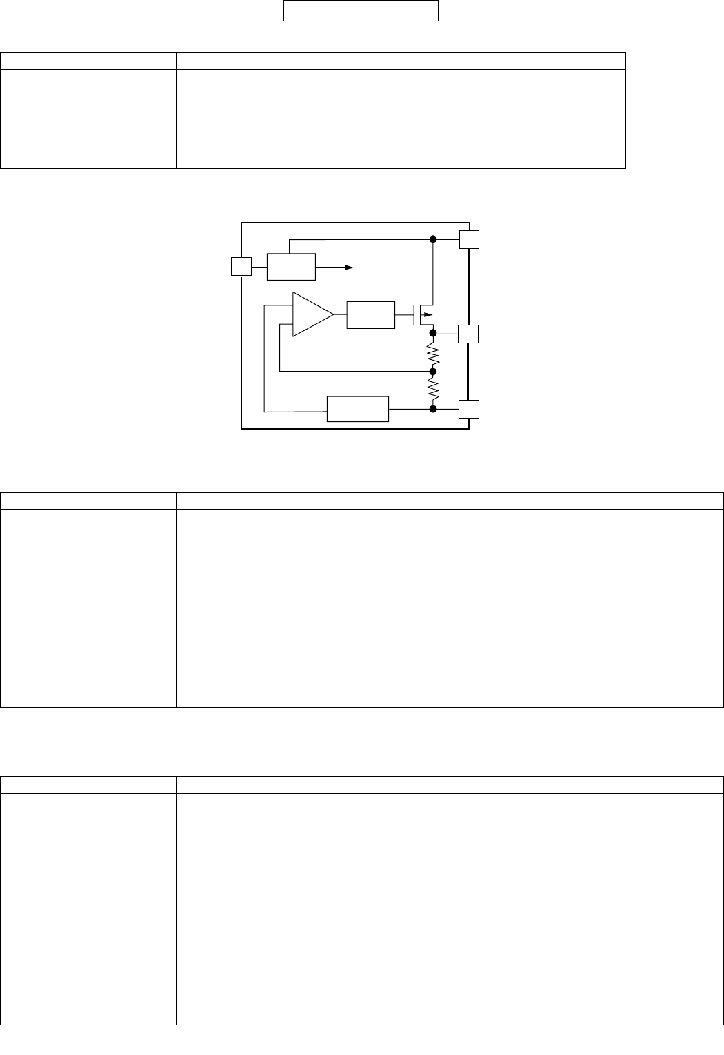
902SH
6 – 18
CONFIDENTIAL
IC1303 VHIXC621933-1L (XC6219C332DR): 3.3 V REGULATOR
In this unit, the terminal with asterisk mark (*) is (open) terminal which is not connected to the outside.
IC1502 VHIBU7876GL-1L (BU7876GL): INFRARED REMOTE Tx CONTROLLER LSI
In this unit, the terminal with asterisk mark (*) is (open) terminal which is not connected to the outside.
IC1504 VHIFA3727R+-1R (FA3727R): POWER CONTROL
Pin No. Terminal name Description of terminal
1 VIN Power supply input
2* NC Not used
3 VOUT Output
4* NC Not used
5 VSS Earth
6 CE ON/OFF control
Pin No. Terminal name Input/Output Description of terminal
1* NC – Mount reinforcement pin (Not used)
2GND – Earth
3 VDD – Power supply
4* NC – Mount reinforcement pin (Not used)
5 DOUT Output Data output
6 NIRQ Output Interrupt output (LOW: interrupt generation)
7* NC – Mount reinforcement pin (Not used)
8 SCL Input IIC bus serial clock (SQL)
9 SDA Input/Output IIC bus serial data input/output
10* NC – Mount reinforcement pin (Not used)
11 NRST Input Reset pin (LOW: reset)
12 CLK1 Input Reference clock input
Pin No. Terminal name Input/Output Description of terminal
1 SNSG – DC/DC converter detection resistance earth
2 VCC – Circuit system power supply input
3 GND2 – Earth
4 VOUT1 Output LDO_1 output
5 VIN1 Input LDO_1 power supply input
6 EN1 Input LDO_1 enable terminal
7 EN4 Input LDO_4 enable terminal
8 VOUT4 Output LDO_4 output
9 VIN2 Input LDO_3, LDO_4 power supply input
10 VOUT3 Output LDO_3 output
11 GND3 – Earth
12 VOUT5 Output LDO_5 output
13 VIN3 Input LDO_2, LDO_5 power supply input
14 VOUT2 Output LDO_2 output
-
+
CE ON/OFF
Control each circuit
Current
Limit
Voltage
Reference
VIN
VOUT
VSS
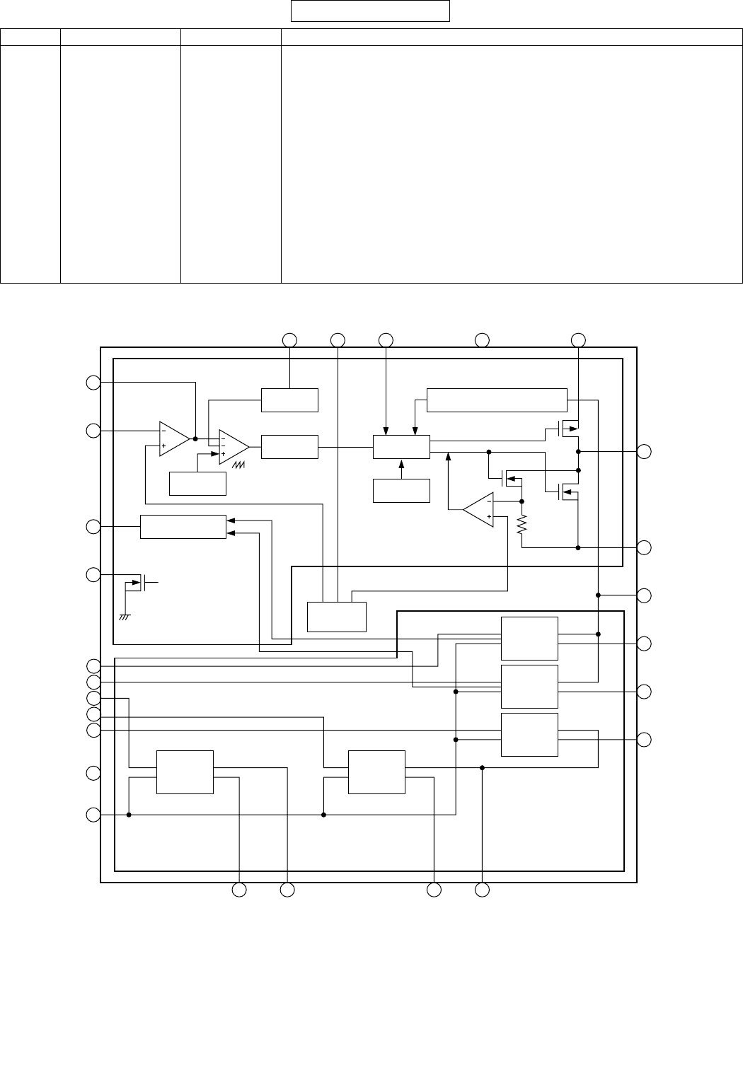
902SH
6 – 19
CONFIDENTIAL
15 EN3 Input LDO_3 enable terminal
16 EN2 Input LDO_2 enable terminal
17 EN5 Input LDO_5 enable terminal
18 CREF – Reference voltage capacitor connection terminal
19 LPM Input Low Power Mode signal input
20 MODE Input Output PchMOS slew mode signal input
21 PGND – Power earth
22 VOUT Output DC/DC converter driver output
23 PVCC – Power system power supply input
24 CS – Soft start terminal
25 GND1 – Earth
26 FB Output Error amplifier output
27 IN- Input Error amplifier inverting input
28 ISNS Input LDO load detection terminal
Pin No. Terminal name Input/Output Description of terminal
Error Amp 1
FB
IN-
VOUT
CS CREF MODE VCC PVCC
PGND
VIN3
VIN2VIN1 VOUT4VOUT1
VOUT2
VOUT5
VOUT3
ISNS
SNSG
EN2
EN5
EN1
EN4
EN3
GND
LPM
Soft Start
Output short-circuit detection
Dead time Pre_driver
enable
OSC UVLO
LDO_2
1.5 V
400 mA
LDO_5
1.5 V
150 mA
LDO_3
2.9 V
300 mA
Load detection
DC/DC Converter
Reference
voltage
Regulator
Comp
LDO_4
2.5 V
200 mA
LDO_1
2.5 V
300 mA
26
27
28
1
16
17
6
7
15
19
45 89
10
12
14
13
21
22
23
2
201824
3, 11, 25

902SH
6 – 20
CONFIDENTIAL
IC1600 VHIYMU783C+-1L (YMU783C): MOBILE AUDIO
Pin No. Terminal name Input/Output Description of terminal
1* NC – Not used
2 GPIO3 Input/Output GPIO port
3 GPIO1 Input/Output GPIO port
4 BCLK Input/Output BIT clock for external audio input
5 D7 Input/Output CPU interface data bus 7
6 D4 Input/Output CPU interface data bus 4
7 D1 Input/Output CPU interface data bus 1
8 D0 Input/Output CPU interface data bus 0
9* NC – Not used
10 MTR Output External vibrator control terminal
11* LED1/GPIO4 Input/Output GPIO port (Not used)
12 GPIO2 Input/Output GPIO port
13 SDI Input External audio input
14 /IRQ Output Interrupt output
15 D5 Input/Output CPU interface data bus 5
16 D2 Input/Output CPU interface data bus 2
17 IOVDD1 – Power supply for terminal
18 DVSS – Digital earth
19 DVDD – Digital core power supply (2.65 to 3.30 V)
20 LED0 Output External LED control terminal 0
21* LED2/GPIO5 Input/Output External LED control terminal 1/GPIO port (Not used)
22 GPIO0 Input/Output GPIO port
23 LRCK Input/Output LR clock for external audio input
24 D6 Input/Output CPU interface data bus 6
25 D3 Input/Output CPU interface data bus 3
26 CLKI Input Clock input terminal (1.5 to 27 MHz): TCXO compatible
27 DVDD – Digital core power supply (2.65 to 3.30 V)
28 DVSS – Digital earth
29 IOVDD2 – Power supply for terminal
30 IOVDD2 – Power supply for terminal
31 IOVDD2 – Power supply for terminal
32 A0 Input CPU interface address signal
33 /CS Input CPU interface chip select
34 /WR Input CPU interface write enable
35 TXOUT Output Transmitted voice analogue output terminal
36 RXIN Input Received voice analogue input terminal
37 /RST Input Hardware reset input
38* NC – Not used
39 /RD Input CPU interface read enable
40 PLLC – PLL capacitance connection terminal for sound source
41 EQ1L – L-ch equaliser terminal 1
42 EQ2L – L-ch equaliser terminal 2
43 EXTIN Input External analogue input terminal
44* NC – Not used
45 EQ2R – R-ch equaliser terminal 2
46 EQ1R – R-ch equaliser terminal 1
47 SPVDDL – Analogue power supply for L-ch speaker amplifier (AVDD to 4.50 V)
48 EQ3L – L-ch equaliser terminal 3
49* NC – Not used
50 HPOUTL/MONO Output L-ch headphone output terminal
51* NC – Not used
52 HPC – Capacitance connection terminal for preventing headphone pop noise
53* NC – Not used
54 EQ3R – R-ch equaliser terminal 3
55 SPVDDR – Analogue power supply for R-ch speaker amplifier (AVDD to 4.50 V)
56 SPVSSL – Analogue earth for L-ch speaker amplifier
57* SPOUT1L – L-ch speaker connection terminal 1 (Not used)
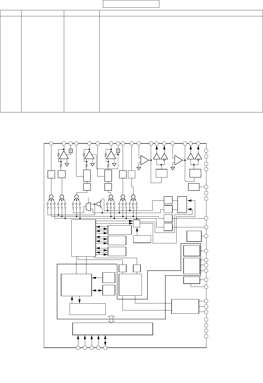
902SH
6 – 21
CONFIDENTIAL
In this unit, the terminal with asterisk mark (*) is (open) terminal which is not connected to the outside.
58* NC – Not used
59 BBR – Capacitance connection terminal for R-ch bus boost (0.1 µF)
60 VREF – Analogue reference voltage terminal
61* EXTOUT Output External analogue output terminal (Not used)
62* NC – Not used
63* SPOUT1R Output R-ch speaker connection terminal 1 (Not used)
64 SPVSSR – Analogue earth for R-ch speaker amplifier
65* (SPOUT1L) Output Internally connected to H2 terminal. H2 terminal is used as SPOUT1L terminal. (Not used)
66* SPOUT2L Output L-ch speaker connection terminal 2 (Not used)
67 BBL Output Capacitance connection terminal for L-ch bus boost (0.1 µF)
68 AVDD – Analogue power supply (2.65 to 3.30 V)
69 AVSS – Analogue earth
70 EXC – Capacitance connection terminal for preventing external output pop noise
71 HPOUTR Output R-ch headphone output terminal
72* SPOUT2R Output R-ch speaker connection terminal 2 (Not used)
73* (SPOUT1R) Output Internally connected to H8 terminal. H8 terminal is used as SPOUT1R terminal. (Not used)
Pin No. Terminal name Input/Output Description of terminal
/CS
/WR
/RD
D0-D7
A0
IOVDD
DVDD
DVSS
GPIO[3:0]
SDI
LRCK
BCLK
CPU I/F
Sampling Rate
Converter
TG
LED
MTR
IRQ
Reset
VREF
VREFVREF
DAC
DVX operation
part
Adder Fader EG
Equalizer
CLKI
PLLC
MTR
LED0
/IRQ
/RST
EXTIN
RXIN
AVDD
AVSS
VREF
SPVDDR
SPVSSR
SPVDDL
SPVSSL
SPOUT2R
SPOUT1R
EQ3R
EQ3L
EQ2L
EQ1R
EQ1L
HPC
HPOUTR
BBR
BBL
EXC
EXTOUT
TXOUT
HPOUTL
/MONO
EQ2R
SPOUT2L
SPOUT1L
LED[2:1]
(GPIO[5:4])
SP
Vol
SP
Vol
VOL
VOL
VOL
VOL BASS
BOOST
BASS
BOOST
VOL
VOL
SRAM
8 k-byte
VOL
VOL
VOL
VOL
VOL
FMR
FML
VOL
X
FMM
MONO
++ +
+-+-+--
+
-
+
+++
+
Wiring switching
Hybrid sound source
(equivalent to MA-5)
Tone
ROM
Sequencer part
(equivalent to MA-5)
MA-5 core
Digital audio
interface
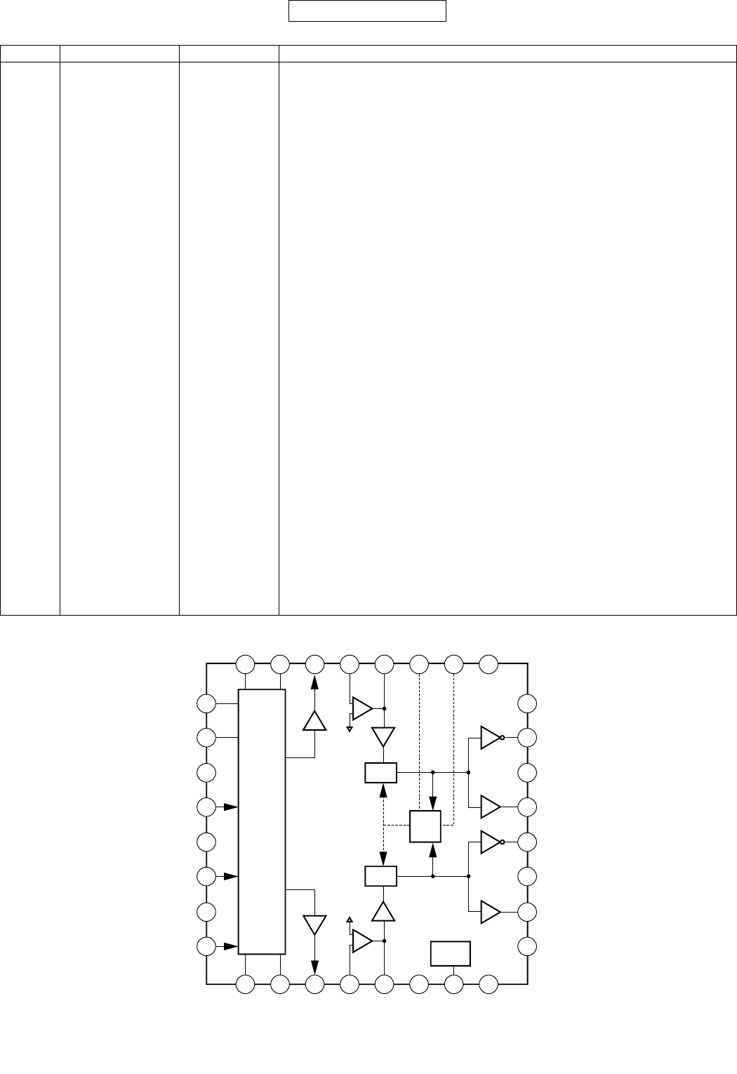
902SH
6 – 22
CONFIDENTIAL
IC1603 (AN12974A): AGC STEREO AMP.
Pin No. Terminal name Input/Output Description of terminal
1 C3 – Surround filter terminal R-ch 1
2 R3 – Surround filter terminal R-ch 2
3 – (Analogue signal) Output Surround output R-ch
4 – (Analogue signal) Output Inverting amplifier output R-ch for gain adjustment
5 – (Analogue signal) Output Inverting amplifier output R-ch for gain adjustment
6 AGC ON/OFF Input AGC ON/OFF switching
7 VREFSP – Precharge timing pin
8 VCC – VCC-SP (R-ch)
9 SP-SAVE Input Speaker power save ON/OFF switching
10 SPOUTR– Output Speaker output R-ch (–)
11 GNDSPR – Earth (SP R-ch)
12 SPOUTR+ Output Speaker output R-ch (+)
13 SPOUTL– Output Speaker output L-ch (–)
14 GNDSPL – Earth (SP L-ch)
15 SPOUTL+ Output Speaker output L-ch (+)
16 STB ON/OFF Input All standby ON/OFF switching
17 VCC – VCC-SP (L-ch)
18 VREFSP – 1/2 VCC-SP (VREF-SP)
19 AGCDET – AGC signal detector
20 – (Analogue signal) Output Inverting amplifier output L-ch for gain adjustment
21 – (Analogue signal) Output Inverting amplifier output L-ch for gain adjustment
22 – (Analogue signal) Output Surround output L-ch
23 R1 – Surround filter terminal L-ch 2
24 C1 – Surround filter terminal L-ch 1
25 C2 – Surround effect adjustment 1
26 R2 – Surround effect adjustment 2
27 VREF – 1/2 VCC (VREF)
28 IN-L Input Sound input terminal L-ch
29 VCC – VCC
30 IN-R Input Sound input terminal R-ch
31 GND – Earth
32 SURROUND ON/
OFF
Input Surround ON/OFF switching
25
26
27
28
29
30
31
32
16
15
14
13
12
11
10
12345 678
24
-6 dB
+6 dB
AGC
AGC
+6 dB
+13 dB
+13 dB
+13 dB
+13 dB
0dB
0dB
-40 dBV
-27 dBV
-27 dBV
-40 dBV
SPATIALIZER®
-34 dBV
-34 dBV-34 dBV
+7 dB+7 dB
-34 dBV
-6 dB
23 22 21 20 19 18 17
9
-
+
-
+
AGC
Det.
Timing
Cont.
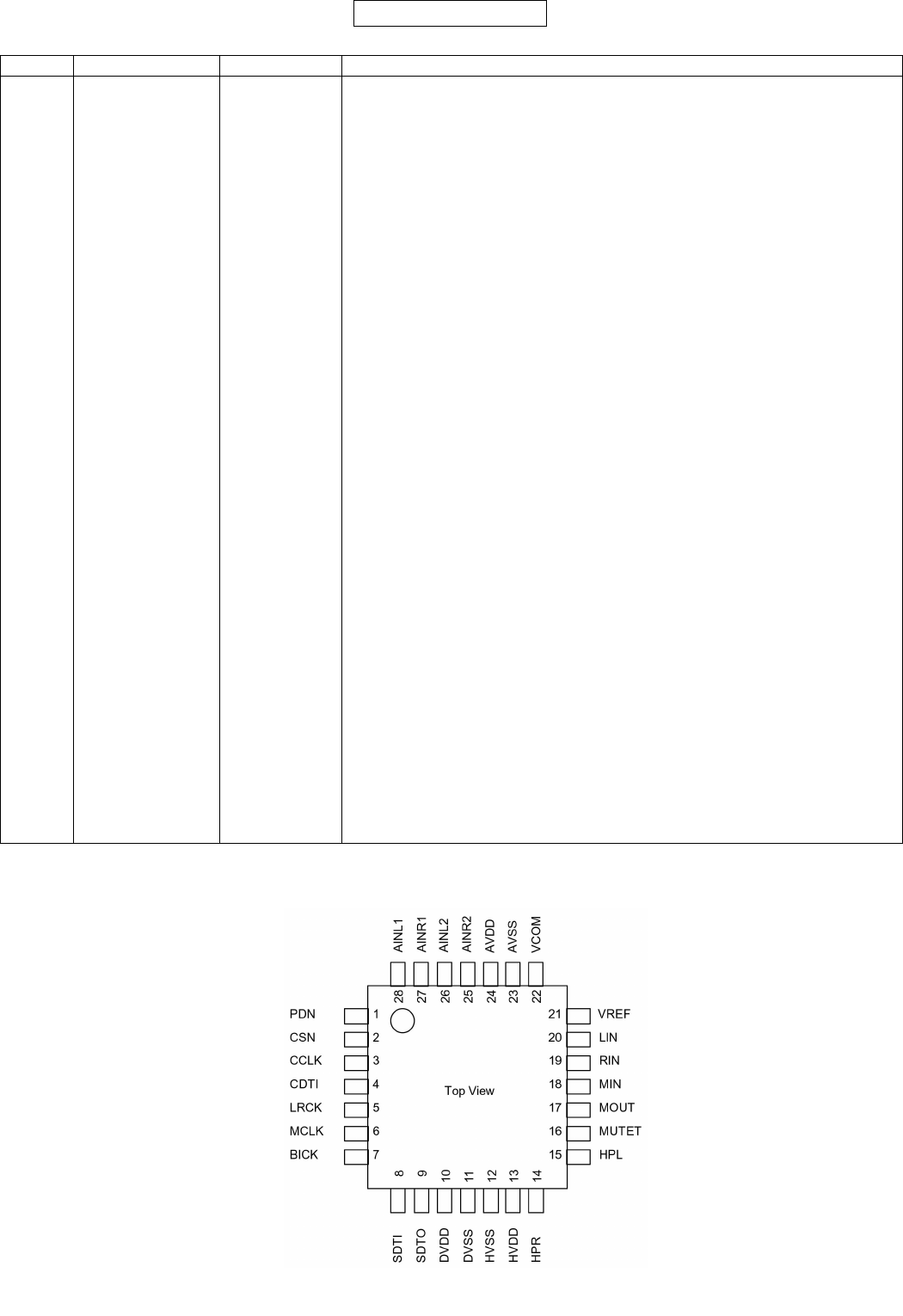
902SH
6 – 23
CONFIDENTIAL
IC1700 VHIAK4569++-1L (AK4569): PCM CODEC
Note: Keep the digital input pin connected.
In this unit, the terminal with asterisk mark (*) is (open) terminal which is not connected to the outside.
Pin No. Terminal name Input/Output Description of terminal
1 PDN Input Power down pin
When this pin is set at “L”, the device is powered down internally and reset. When the
power is turned on, input “L” once.
2 CSN Input Control data chip select pin
3 CCLK Input Control clock input pin
4 CDTI Input Control data input pin
5 LRCK Input L/R clock pin
Determines an audio data channel
6 MCLK Input Master clock input pin
7 BICK Input Serial bit clock pin
Clock for shifting audio data
8 SDTI Input Audio data input pin
9 SDTO Output Audio data output pin
When PMADC bit = “0”, pin SDTO is DVSS
10 DVDD –Digital power supply pin
11 DVSS –Digital earth pin
12 HVSS –Earth pin for headphone amplifier
13 HVDD –Power supply pin for headphone amplifier
14* HPR Output R-ch HP-Amp output pin (Not used)
When PMHPR bit = “0”, pin HPR is HVSS
15* HPL Output L-ch HP-Amp output pin (Not used)
When PMHPL bit = “0”, pin HPL is HVSS
16 MUTET Output Mute time constant control pin
When PMHPL bit = PMHPR bit = “0”, pin MUTET is HVSS
17* MOUT Output Monaural analogue output pin (Not used)
When PMMO bit = “0”, pin MOUT is Hi-Z
18 MIN Input Monaural analogue input pin
19 RIN Input R-ch analogue input pin
20 LIN Input L-ch analogue input pin
21 VREF Output Reference voltage output pin, 2.1 V (referenced to typ. AVSS)
When PMVCM bit = “0”, pin VREF is AVSS
22 VCOM Output Common voltage pin, 1.25 V (referenced to typ. AVSS)
When PMVCM bit = “0”, pin VCOM is AVSS
23 AVSS –Analogue earth pin
24 AVDD –Analogue power supply pin
25 AINR2 Input ADC R-ch analogue input 2 (MIC input)
26 AINL2 Input ADC L-ch analogue input 2 (MIC input)
27 AINR1 Input ADC R-ch analogue input 1 (LINE input)
28 AINL1 Input ADC L-ch analogue input 1 (LINE input)

902SH
6 – 24
CONFIDENTIAL
IC1701 VHIMM1671XN-1R (MM1671XN): VIDEO AMP.
Pin No. Terminal name Description of terminal
1 PS Power save
2 OUT Signal output
3 SAG Sag correction
4 IN Signal input
5GND Earth
6 VCC (V+) Power supply
1
2
34
5
6
Top View
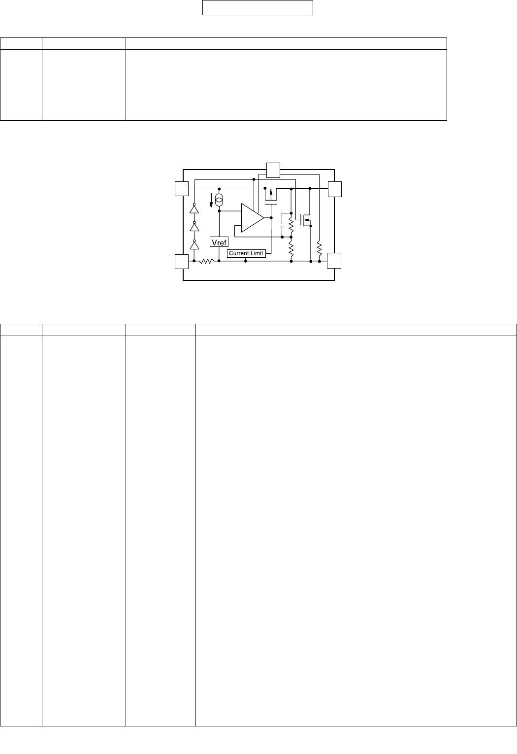
902SH
6 – 25
CONFIDENTIAL
IC2001 VHIR116129D-1L (R1161D291D): SD POWER CONTROL
In this unit, the terminal with asterisk mark (*) is (open) terminal which is not connected to the outside.
IC2002 RH-IX3067AFZZL (BD6020): COMPOUND POWER SUPPLY 2
Pin No. Terminal name Description of terminal
1 VDD (VIN) Input pin
2* NC Not used
3 VOUT Output pin
4 ECO High speed, low power switch
5GND Earth
6 /CE or CE Chip enable pin
Pin No. Terminal name Input/Output Description of terminal
1 GNDT1 – Test pin (GND internal connection)
2 VBAT1 – Negative boost DC/DC power supply pin
3 GND1 – Earth power supply pin
4 VIO – CPU I/F constant current driver power supply pin
5 CLK Input Three-wire serial clock input
6 RSTB Input Reset input
7 T2 – Test pin (connected to T4)
8 VNEG Input Negative boost DC/DC output voltage detection pin
9* NC – Not used
10 TRSW Output Switching Tr drive pin of negative boost DC/DC
11 DATA Input Three-wire serial data input
12 STRB Input Three-wire serial strobe input
13* TEST1 Input Test pin (Not used)
14 VOUT1 Output REG1 output
15 SENSEN1 Input Switching Tr current sense pin of negative boost DC/DC
16 SENSEN2 Input Test pin
17 VBAT2B – REG1/REG2/VREF power supply pin
18 VBAT2A – REG1/REG2/VREF power supply pin (VIN)
19 SENSP2 Input Test pin
20 SENSP1 Input Switching Tr current sense pin of negative boost DC/DC
21* TEST2 Input Test pin (Not used)
22 VOUT2 Output REG2 output
23 CNTOUT Output External regulator control output
24 VSEL2 Input REG2 output voltage switching pin
25 VREF Output Voltage reference & smoothing capacitor connection pin
26 CURSENS Input Current detection pin for constant current drive
27 GNDP – Earth
28 GND3 – Earth
29 VBAT3 – Boost DC/DC power supply pin
30 REG2CNT Input REG2 control pin
31 VPLUS11 Input REGCP power supply pin
32 GND2 – Earth
33* CUR Output Transistor drive pin for constant current drive control (Not used)
+
-
VDD
/CE GND
VOUT
ECO
902SH
6 – 26
CONFIDENTIAL
In this unit, the terminal with asterisk mark (*) is (open) terminal which is not connected to the outside.
IC2003 RH-IX3068AFZZL (BD6030): COMPOUND POWER SUPPLY 3
In this unit, the terminal with asterisk mark (*) is (open) terminal which is not connected to the outside.
34 T4 – Test pin (connected to T2)
35 SW Output Boost DC/DC switching pin
36 VBATP – Boost DC/DC driver power supply pin
37 REG1CNT Input REG1 control pin
38 VPLUS12 Input Boost DC/DC voltage detection pin
39 CAMP Output REGCP output
40 GNDT3 – Test pin
Pin No. Terminal name Input/Output Description of terminal
1* NC – Not used
2GND – Earth
3 PD Input Power control pin
4* NC – Not used
5 VSEL Input Output voltage switching pin
6 VBAT Input VBAT power supply pin
7* NC – Not used
8* VREF (NC) Output Reference voltage output pin (Not used)
9 VOUT Output Negative voltage output
10* NC – Not used
11 VNEG – Negative power supply pin
12 VSUB – Test pin
Pin No. Terminal name Input/Output Description of terminal
1234567
8 9 10 11
TOP VIEW
12 13 14
15 16 17 18
19 20 21 22
23 24 25 26
27 28 29 30 31 32 33
34 35 36 37 38 39 40
123
TOP VIEW
4
12 5
11 6
10 9 8 7

902SH
6 – 27
CONFIDENTIAL
IC2005 RH-IXA021AFZZL (BD6015GU): COMPOUND POWER SUPPLY 1
In this unit, the terminal with asterisk mark (*) is (open) terminal which is not connected to the outside.
Pin No. Terminal name Input/Output Description of terminal
1T1 – Dummy pin
2 LEDG Output Green LED drive output pin
3 GND1 – Earth
4 VBAT1 – VBAT power supply pin
5* LSO11 Output Level shift output 1 (Not used)
6* LSO12 Output Level shift output 1 (Not used)
7 WVOUT Output 2 or 4 times boost charge pump output
8T2 – Dummy pin
9 TEST Input Test pin
10 LEDR Output Red LED drive output pin
11 LEDB Output Blue LED drive output pin
12 TRSW Output DC-DC switching transistor drive pin for R/G/B LED
13 CAPP1 Output 2 or 4 times boost charge pump C1 connection pin
14* CAPN1 Output 2 or 4 times boost charge pump C1 connection pin (Not used)
15 SENSP Input DC-DC switching transistor current sense pin for R/G/B LED
16 SENSN Input DC-DC switching transistor current sense pin for R/G/B LED
17 CAP3 Output 2 or 4 times boost charge pump output pin
18 CPIN Input 2 or 4 times boost charge pump input pin
19 CAPP2 Output 2 or 4 times boost charge pump C2 connection pin
20 VIO – Logic system power supply pin
21 VPLUS2 Input DC-DC boost voltage feedback input for R/G/B LED
22* CAPN2 Output 2 or 4 times boost charge pump (Not used)
23 GND3 – Earth
24 STRB Input Three-wire serial strobe input
25 CLK Input Three-wire serial clock input
26 VPLUS12 Input DC-DC boost voltage feedback input for Main Display/Sub Display backlight
27* CAMP Output 15 V voltage output pin for camera (Not used)
28 DATA Input Three-wire serial data input
29 FRP Input Level shift circuit, rectangular wave input pin
30 IREF Output Resistance connection pin for current reference
31 VREF Output Current reference pin
32 LEDCTL Input R/G/B LED On/Off control pin
33* ERROUT Output SWREG1 error detection amplifier output (Not used)
34 FLED Output Main Display backlight white LED drive pin
35 GND2 – Earth
36* SBD Input SBD input pin (Not used)
37 VNEG Input Negative power supply pin for camera
38* CAMN Output –8 V voltage output pin for camera (Not used)
39 T4 – Dummy pin
40 RSTB Input Reset input
41 BLED Output Sub Display backlight white LED drive pin
42 SW Output DC-DC coil switching pin for Main Display/Sub Display backlight
43 GNDP Output Earth
44 VBAT2 – VBAT power supply pin
45 VPLUS11 Input DC-DC boost voltage feedback input for Main Display/Sub Display backlight
46 T3 – Dummy pin
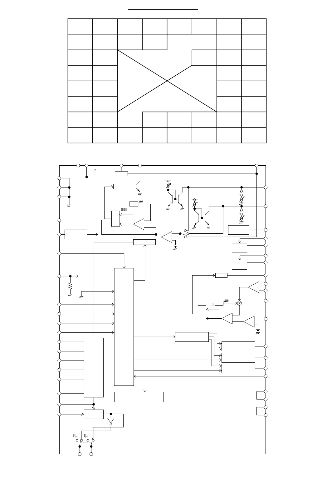
902SH
6 – 28
CONFIDENTIAL
A
B
C
D
E
F
G
H
T1
TEST
SENSP
VIO
STRB
DATA
LEDCTL
T4
1
LEDG
LEDR
SENSN
VPLUS2
CLK
FRP
ERROUT
RSTB
2
GND1
LEDB
BLED
3
VBAT1
TRSW
FLED
SW
4
LSO11
GND2
GNDP
5
LSO12
CAP3
SBD
VBAT2
6
WVOUT
CAPP1
CPIN
CAPN2
VPLUS12
IREF
VNEG
VPLUS11
7
T2
CAPN1
CAPP2
GND3
CAMP
VREF
CAMN
T3
8
2
10
16
21
25
29
33
40
3
11
41
4
12
34
42
5
35
43
6
17
36
44
7
13
18
22
26
30
37
45
8
14
19
23
27
31
38
46
1
9
15
20
24
28
32
39
Level
Shift
Current
Reference
LDO
..8.0V
LDO
15.0V
Shut Down Control
(with Thermal Shut Down)
Voltage
Reference
Oscillator
LDO
Vref
Control
Logic
S9
-
+
-
+
+
-
+
-
+
+
+
-
Osc
Driver
Driver
O
S
R
O
S
R
Osc
100 kohm
LSO11
GNDP
GND1
GND2
ERROUT
VREF
VIO
TEST
DATA
CLK
STRB
RSTB
CPIN
CAPP1
CAPN1
CAPP2
CAPN2
CAP3
WVOUT
FRP
LSO12
VBAT2 VBAT1 SBD SW VPLUS11
BLED
FLED
IREF
VPLUS12
CAMP
CAMN
TRSW
SENSP
SENSN
GND3
VPLUS2
LEDR
LEDG
LEDB
LEDCTL
T1
T2
T3
T4
VNEG
Constant Current
Regulator Circuit
Constant Current
Drive Circuit
Constant Current
Drive Circuit
Constant Current
Drive Circuit
4 times
Boost
Charge
Pump

902SH
6 – 29
CONFIDENTIAL
IC3000 (LR38866): DISPLAY CONTROLLER
Pin No. Terminal name Input/Output Description of terminal
1 DUMMY4 – Dummy 4
2 VDDCORE – Power supply
3 BSPIXEL3/NDATA3 TYBUF03P (A) BS: external BitStream data bus
NTSC: NTSC encoder output
4 BSPIXEL5/NDATA5 TYBUF03P (A) BS: external BitStream data bus
NTSC: NTSC encoder output
5 VDDIOB – Power supply
6 BSHS_B/HSYNC_NT TYBUF03S (O) BS: external BitStream horizontal sync signal
NTSC: horizontal sync signal
7 OSCIN PDX0E1DG Oscillating circuit input
8 VDDOSC – Power supply
9* SUBCS_B/
SUBGPO3
TYBUF04P Sub Display chip select (STN/TFT control)/general purpose output (Not used)
10* SUBDB4 TYBUF04P Sub Display data bus (STN/TFT control) (Not used)
11 VDDIOD – Power supply
12* SUBDB7 TYBUF04P Sub Display data bus (STN/TFT control) (Not used)
13* SUBRS/SUBGPO2 TYBUF04P Sub Display data recognition signal (STN/TFT control)/general purpose output (Not used)
14 VDDIOD – Power supply
15 SUBFLMIN TYBUF02P Sub Display FLM signal (STN control)
16 DUMMY3 – Dummy 3
17 BSPIXEL2/NDATA2 TYBUF03P (A) BS: external BitStream data bus
NTSC: NTSC encoder output
18 VDDCORE – Power supply
19 BSPIXEL4/NDATA4 TYBUF03P (A) BS: external BitStream data bus
NTSC: NTSC encoder output
20 BSPIXEL6/NDATA6 TYBUF03P (A) BS: external BitStream data bus
NTSC: NTSC encoder output
21 BSBLK_B TYBUF03S (A) External BitStream data valid signal
22 BSVS_B/VSYNC_NT TYBUF03S (O) BS: external BitStream vertical sync signal
NTSC: vertical sync signal
23* OSCOUT PDX0E1DG Oscillating circuit output (Not used)
24* GPO8 TYBUF04P General purpose output (Not used)
25* SUBDB0 TYBUF04P Sub Display data bus (STN/TFT control) (Not used)
26* SUBDB3 TYBUF04P Sub Display data bus (STN/TFT control) (Not used)
27* SUBDB5 TYBUF04P Sub Display data bus (STN/TFT control) (Not used)
28* SUBCK/SUBGPO1 TYBUF04P Sub Display clock (STN/TFT control)/general purpose output (Not used)
29* SUBRD_B/
SUBGPO5
TYBUF04P Sub Display read signal (STN/TFT control)/general purpose output (Not used)
30 VDDCORE – Power supply
31* SUBCKS/SUBGPO0 TYBUF04P Clock switching signal for Sub Display (STN/TFT control)/general purpose output (Not
used)
32 VDDPLL – Power supply
33 VDDIOB – Power supply
34 BSPIXEL1/NDATA1 TYBUF03P (A) BS: external BitStream data bus
NTSC: NTSC encoder output
35 PLLDIV2 TYBUF04P PLL multiplication ratio switching signal
36 PLLDIV0 TYBUF04P PLL multiplication ratio switching signal
37 BSPIXEL0/NDATA0 TYBUF03P (A) BS: external BitStream data bus
NTSC: NTSC encoder output
38 NTCLK TYBUF02S External supply clock
39* NC – Not used
40 BSPIXEL7/NDATA7 TYBUF03P (A) BS: external BitStream data bus
NTSC: NTSC encoder output
41 BSCLK/DCLK_NT TYBUF03S (A) BS: external BitStream data clock
NTSC: data sampling clock
42* GPO9 TYBUF04P General purpose output (Not used)
43* SUBWR_B/
SUBGPO4
TYBUF04P Sub Display write signal (STN/TFT control)/general purpose output (Not used)
44* SUBDB1 TYBUF04P Sub Display data bus (STN/TFT control) (Not used)
45* SUBDB2 TYBUF04P Sub Display data bus (STN/TFT control) (Not used)

902SH
6 – 30
CONFIDENTIAL
46* SUBDB6 TYBUF04P Sub Display data bus (STN/TFT control) (Not used)
47 SUBLPIN TYBUF02P Sub Display LP signal (STN control)
48* NC – Not used
49 PLLDIV1 TYBUF04P PLL multiplication ratio switching signal
50 XIN/SCANCK TYBUF02S External clock input signal
51 BDATA4 TYBUF04P Main Display panel B output signal
52 BDATA5 TYBUF04P Main Display panel B output signal
53* GPO5 TYBUF04P General purpose output (Not used)
54 GND – Earth
55 GND – Earth
56 GNDOSC – Earth
57* NC – Not used
58* NC – Not used
59 GND – Earth
60* NC – Not used
61 GND – Earth
62 SCL TYBUF04S I2C serial clock pin
63 GPI4 TYBUF02S_PD General purpose input
64 VDDCORE – Power supply
65 VDDIOB – Power supply
66 BDATA3 TYBUF04P Main Display panel B output signal
67 BDATA2 TYBUF04P Main Display panel B output signal
68 BDATA1 TYBUF04P Main Display panel B output signal
69 GNDPLL – Earth
70 SDA TYBUF04S I2C serial data pin
71* WAIT_B TYBUF02P External wait signal (Not used)
72 LCDINT TYBUF02P External interruption signal
73 BDATA0 TYBUF04P Main Display panel B output signal
74* GPO4 TYBUF04P General purpose output (Not used)
75 GDATA0 TYBUF04P Main Display panel G output signal
76 GND – Earth
77* NC – Not used
78 DB15 TYBUF03P (A) Parallel data bus
79 GPI5 TYBUF02S_PD General purpose input
80 GPO7 TYBUF04P General purpose output
81 GDATA1 TYBUF04P Main Display panel G output signal
82 GDATA2 TYBUF04P Main Display panel G output signal
83 GDATA3 TYBUF04P Main Display panel G output signal
84* NC – Not used
85 GND – Earth
86 DB12 TYBUF03P (A) Parallel data bus
87 DB14 TYBUF03P (A) Parallel data bus
88 VDDIOA – Power supply
89 VDDIOB – Power supply
90 GDATA4 TYBUF04P Main Display panel G output signal
91 GDATA5 TYBUF04P Main Display panel G output signal
92 GND – Earth
93 TESTI TYBUF02P_PD Test signal
94 DB11 TYBUF03P (A) Parallel data bus
95 DB10 TYBUF03P (A) Parallel data bus
96 DB13 TYBUF03P (A) Parallel data bus
97 RDATA0 TYBUF04P Main Display panel R output signal
98 RDATA1 TYBUF04P Main Display panel R output signal
99 GPO1 TYBUF04P General purpose output
100* NC – Not used
101 GND – Earth
102* GPCLK TYBUF04P General purpose clock output (Not used)
103 DB9 TYBUF03P (A) Parallel data bus
104* GPO6 TYBUF04P General purpose output (Not used)
Pin No. Terminal name Input/Output Description of terminal

902SH
6 – 31
CONFIDENTIAL
105 RDATA2 TYBUF04P Main Display panel R output signal
106 RDATA3 TYBUF04P Main Display panel R output signal
107 RDATA4 TYBUF04P Main Display panel R output signal
108 GND – Earth
109 SCANEN TYBUF02P_PD Full scan valid signal
110 DB7 TYBUF03P (A) Parallel data bus
111 DB8 TYBUF03P (A) Parallel data bus
112 VDDIOA – Power supply
113 VDDIOB – Power supply
114 RDATA5 TYBUF04P Main Display panel R output signal
115 VSYNC TYBUF02P Main Display vertical sync signal
116 GND – Earth
117* GPO10 TYBUF04P General purpose output (Not used)
118 GND – Earth
119* NC – Not used
120 GNDVD – Earth
121* NC – Not used
122 GND – Earth
123* NC – Not used
124 DB5 TYBUF03P (A) Parallel data bus
125 DB4 TYBUF03P (A) Parallel data bus
126 DB6 TYBUF03P (A) Parallel data bus
127 DCLK TYBUF02P Main Display data sampling clock
128 HSYNC TYBUF02P Main Display horizontal sync signal
129* NC – Not used
130* SE_LD4/PORT5 TYBUF04P Four-wire serial IF load signal 4/general purpose output (Not used)
131* GPO11 TYBUF04P General purpose output (Not used)
132 GPI3 TYBUF02S_PU General purpose input
133 GPI1 TYBUF02S_PU General purpose input
134 RXDTP RECIVER_V3.4 Differential data input (Positive)
135 RXDTN RECIVER_V3.4 Differential data input (Negative)
136 VDWAIT_B TYBUF02P External wait signal
137 RSP TYBUF03S (A) Register select signal
138* MAGBUSY TYBUF04P Magnification circuit LINE direction BUSY output (Not used)
139 DB3 TYBUF03P (A) Parallel data bus
140 DB2 TYBUF03P (A) Parallel data bus
141* GPO3 TYBUF04P General purpose output (Not used)
142* GPO2 TYBUF04P General purpose output (Not used)
143 DB1 TYBUF03P (A) Parallel data bus
144 VDDIOA – Power supply
145 VDDCORE – Power supply
146 VDDCORE – Power supply
147 SE_DO/PORT0 TYBUF04P Four-wire serial IF data output/general purpose output
148 SE_LD1/PORT2 TYBUF04P Four-wire serial IF load signal 1/general purpose output
149* SE_LD3/PORT4 TYBUF04P Four-wire serial IF load signal 3/general purpose output (Not used)
150* PWMLCD/PORT9 TYBUF04P PWMLCD output/general purpose output (Not used)
151* PWM0/PORT7 TYBUF04P PWM output 0/general purpose output (Not used)
152 GPI0 TYBUF02S_PU General purpose input
153 RXCKP RECIVER_V3.4 Differential clock input (Positive)
154 RXCKN RECIVER_V3.4 Differential clock input (Negative)
155 GPO0 TYBUF04P General purpose output
156 VD0N TYBUF02P VD-Link ON/OFF setting
157 CS_B TYBUS03S (O) Device select signal
158 WR_B TYBUF03S (O) Host write strobe signal
159 VDDCORE – Power supply
160 DB0 TYBUF03P (A) Parallel data bus
161 DUMMY2 – Dummy 2
162 SE_DI/PORT6 TYBUF04P Four-wire serial input/general purpose output
163 VDDIOC – Power supply
Pin No. Terminal name Input/Output Description of terminal
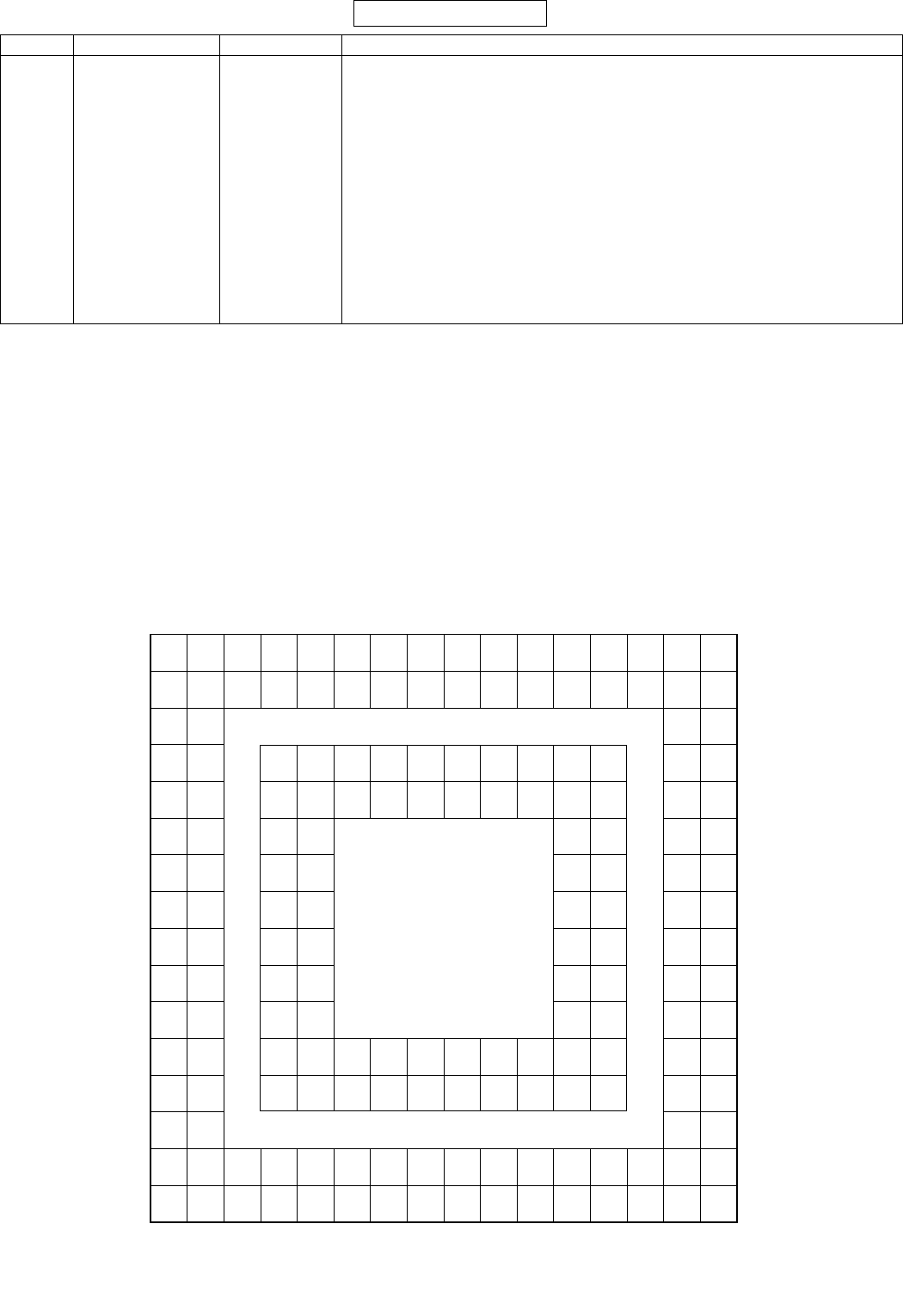
902SH
6 – 32
CONFIDENTIAL
In this unit, the terminal with asterisk mark (*) is (open) terminal which is not connected to the outside.
164 SE_CK/PORT1 TYBUF04P Four-wire serial IF clock output/general purpose output
165* SE_LD2/PORT3 TYBUF04P Four-wire serial IF load signal 2/general purpose output (Not used)
166 VDDIOC – Power supply
167* PWM1/PORT8 TYBUF04P PWM output 1/general purpose output (Not used)
168 GPI2 TYBUF02S_PU General purpose input
169 GSR RECIVER_V3.4 External resistance pin for gain adjustment
170 VDDVD – Power supply
171 RESET_B TYBUF02S Master reset
172 VDDIOA – Power supply
173 BUFOFF_B TYBUF02P GATED buffer switching signal for through current protection
174 RD_B TYBUF03S (O) Host read strobe signal
175 VDDCORE – Power supply
176 DUMMY1 – Dummy 1
PDX0E1DG : OSC (Oscillator buffer with oscillation stop function)
TYBUF04P : IOC2M (I/O buffer. Input: CMOS buffer, Output: Iol = 2 mA)
TYBUF04S : IOCS2M (I/O buffer. Input: CMOS Schmidt buffer, Output: Iol = 2 mA)
TYBUF02P : IOC (I/O buffer. Input: CMOS buffer, Output: Iol = 4 mA)
TYBUF02P_PD : IOCD (I/O buffer. Input: CMOS buffer with 65 k ohm pull-down resistance, Output: Iol = 4 mA)
TYBUF02S : IOCS (I/O buffer. Input: CMOS Schmidt buffer, Output: Iol = 4 mA)
TYBUF02S_PU : IOCSU (I/O buffer. Input: CMOS Schmidt buffer with 75 k ohm pull-up resistance, Output: Iol = 4 mA)
TYBUF02S_PD : IOCSD (I/O buffer. Input: CMOS Schmidt buffer with 65 k ohm pull-down resistance, Output: Iol = 4 mA)
TYBUF03P (A) : IOCAN6M (I/O buffer. Input: 2 inputs AND type CMOS buffer with through current protection, Output: Iol = 6 mA)
TYBUF03S (A) : IOCSAN6M (I/O buffer. Input: 2 inputs AND type CMOS Schmidt buffer with through current protection, Output: Iol = 6 mA)
TYBUF03S (O) : IOCSOR6M (I/O buffer. Input: 2 inputs OR type CMOS Schmidt buffer with through current protection, Output: Iol = 6 mA)
RECIVER_V3.4 : VD-Link receiver
Pin No. Terminal name Input/Output Description of terminal
DUMMY
1
DUMMY
3
DUMMY
4
SUBFL
MIN
DUMMY
2
VDD
CORE
VDD
IOA
VDD
IOA
VDD
IOA
LCD
INT
WAIT
_B
GND
PLL
RDATA
1
RDATA
2
RDATA
3
B DATA
5
B DATA
4
VDD
IOB
VDD
IOB
SCANE
N
RDATA
4
RDATA
3
RDATA
2
RDATA
1
GDATA
5
GDATA
3
GDATA
0
GDATA
2
GDATA
1
GDATA
4
VDD
IOB
BDATA
0
RDATA
0
MAG
BUSY
VDWAIT
_B
SE_LD4
/PORT5
SUBDB
7
MP4_PL
LCK
VDD
CORE
VDD
CORE
VDD
CORE
VDD
IOD
VDD
IOB
VDD
IOD
VDD
OSC
OSC
IN
BSHS
_B
VDD
CORE
VDD
CORE
XIN/
SCANCK
PLL
DIV1
PLL
DIV0
VDD
PLL
SUB
CKS
SUB
CK
SUB
DB5
SUB
DB3
SUB
DB0
OSC
OUT
BSVS
_B
BSBLK
_B
SUB
RD_B
SUB
RS
SUB
DB7
SUB
DB4
SUB
CS_B
PLL
DIV2
SUB
LPIN
SUB
DB6
SUB
DB2
SUB
DB1
SUB
WR_B
BSPIXE
L7
BSPIXE
L0
BSPIXE
L1
BSPIXE
L5
BSPIXE
L3
BSPIXE
L4
BSPIXE
L6
BSPIXE
L2
GND
OSC
VDD
CORE
VDD
CORE
PWM0/
PORT7
SE_LD3
/PORT4
SE_LD1
/PORT2
SE_DO
/PORT0
PWMLCD
/PORT9
BUFOF
F_B
VDD
IOA
VDD
VD
VDD
IOC
VDD
IOC
PWM1/
PORT8
SE_LD2
/PORT3
SE_CK/
PORT1
SE_DI/
PORT6
RESET
_B
RD_8
DB00
DB01
DB02 DB03
DB06
GPO6
DB13 DB10
DB14
GPO7
GPI5
GPI4 SCL GND GND GND GND GPO5NC
NC
GPO9
GPO8
NC
NTCLKBSCLK
NC NC
DB15
SDA
NC GND
GPO4
DB12 GND NC
DB11 GND
TESTI
GPO1
DB04
DB08
DB09 GND NC
GPCLK
DB07 GND
DB05 GND GND GND
GNDVD
NC NC
GPO10
VSYNC
NC
RSP
RXDTN
GPI1 GPI3 NC DCLK
GPO11
HSYNCRXDTP
GPO2 GPO3
WR_B VDON GPO0 GPI0
RXCKN RXCKP
CS_B
GSR GPI2
16 15 14 13 12 11 10 9 8 7 6 5 4 3 2 1
A
B
C
D
E
F
G
H
I
J
K
L
M
N
O
P
TOP VIEW
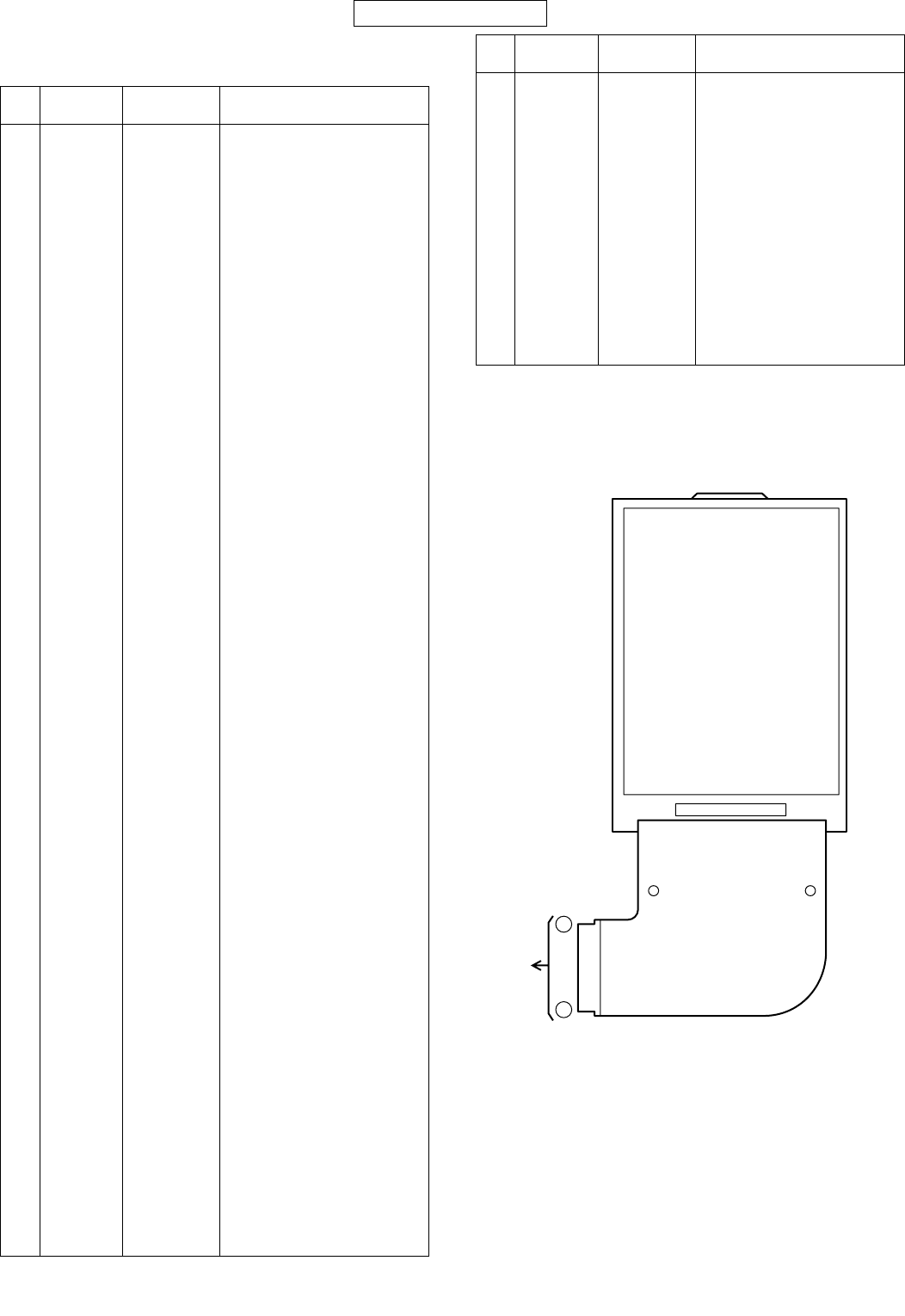
902SH
6 – 33
CONFIDENTIAL
[2] Function table of Display
Main Display (LCD3000: RLCUBA017AF02)
In this unit, the terminal with asterisk mark (*) is (open) terminal which
is not connected to the outside.
Pin
No.
Terminal
name
Input/Output Description of terminal
1 T-COM Input COM electric potential input for
CS
2 T-COM Input COM electric potential input for
CS
3 TFT-COM Input COM voltage input terminal
4 COMC Output COM signal output
5 COMC Output COM signal output
6 COMDC Output COM centre voltage output
7 VCOMH Output COM amplitude voltage output
8 B0 Input Blue data signal (LSB)
9 B1 Input Blue data signal
10 B2 Input Blue data signal
11 B3 Input Blue data signal
12 B4 Input Blue data signal
13 B5 Input Blue data signal (MSB)
14 G0 Input Green data signal (LSB)
15 G1 Input Green data signal
16 G2 Input Green data signal
17 G3 Input Green data signal
18 G4 Input Green data signal
19 G5 Input Green data signal (MSB)
20 R0 Input Red data signal (LSB)
21 R1 Input Red data signal
22 R2 Input Red data signal
23 R3 Input Red data signal
24 R4 Input Red data signal
25 R5 Input Red data signal (MSB)
26 DCLK Input Data sampling clock
27 HSY Input Horizontal sync signal
28 VSY Input Vertical sync signal
29* SO Output Serial data output (Not used)
30 SI Input Serial data input
31 SCLK Input Serial clock input
32 CS Input Serial interface chip select
33 RESET Input Hard reset
34 VCC – Logic power supply
35 GND – Earth
36 GND – Earth
37 VDC – Analogue power supply
38 VDC – Analogue power supply
39* COM2 – Not used
40* VCLAMP Output Not used
41 VSS2 Output DC/DC converter output
42 VSS1 Output DC/DC converter output
43* NC – Not used
44 VDD2 Output DC/DC converter output
45 C5- – Booster capacitor connection
terminal
46 C5+ – Booster capacitor connection
terminal
47 C4- – Booster capacitor connection
terminal
48 C4+ – Booster capacitor connection
terminal
49* C3- – Booster capacitor connection
terminal (Not used)
50 C3+ – Booster capacitor connection
terminal
51 C2- – Booster capacitor connection
terminal
52 C2+ – Booster capacitor connection
terminal
53 C1- – Booster capacitor connection
terminal
54 C1+ – Booster capacitor connection
terminal
55 VDC2 Output DC/DC converter output
56 VDC2 Output DC/DC converter output
57 VR Output Reference power supply output
58 VS Output Source power supply output
59 VS Output Source power supply output
Pin
No.
Terminal
name
Input/Output Description of terminal
1
59
To input terminal
MAIN DISPLAY
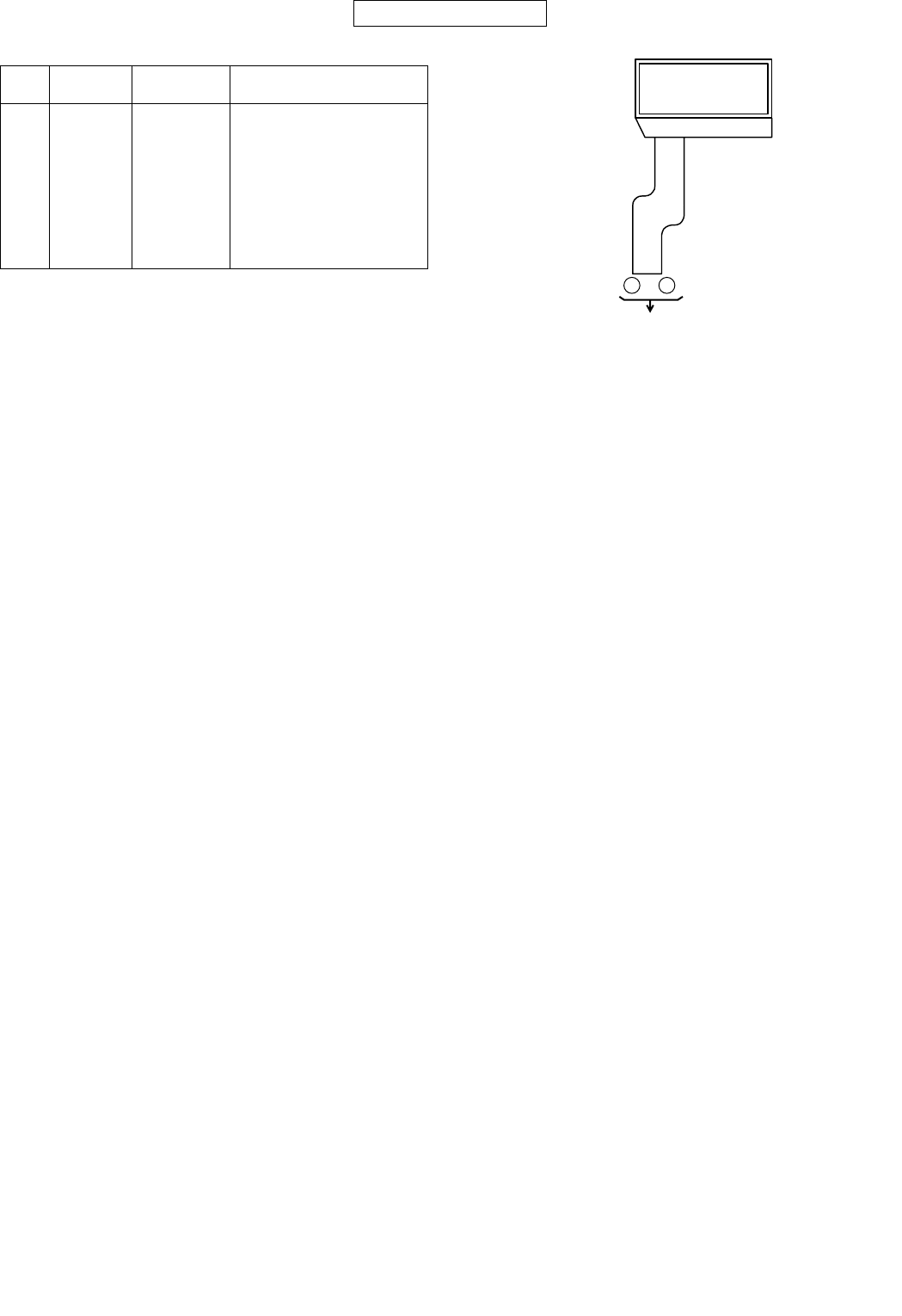
902SH
6 – 34
CONFIDENTIAL
Sub Display (LCD2000: RLCUBA016AFZZ)
Pin
No.
Terminal
name
Input/Output Description of terminal
1 SDIN Input Serial data input
2 SCLK Input Serial clock input
3 DC_B Input Data/command selection input
4 SCEB Input Chip enable
5 RESET_B Input Reset input
6 VDD – MPU power supply terminal
7 VLCD – LCD drive circuit power supply
8VSS – Earth
1
8
To input terminal
SUB DISPLAY

PARTS GUIDE
No. S0422JNJ300/W
SHARP CORPORATION
SHARP CORPORATIONSHARP CORPORATION
SHARP CORPORATION
CONTENTS
Parts marked with " " are important for maintaining the safety of the set. Be sure to replace these
parts with specified ones for maintaining the safety and performance of the set.
902SH
This document has been published to be used
for after sales service only.
The contents are subject to change without notice.
3G(UMTS)/GSM/GPRS PHONE
MODEL 902SH
[1] DIODES
[2] OTHER CIRCUITRY
PARTS
[3] CABINET PARTS
[4] ACCESSORIES/PACKING
PARTS
[5] P.W.B. ASSEMBLY
[6] OTHER SERVICE PARTS
CONFIDENTIAL

902SH
2
NO. PARTS CODE PRICE
RANK
NEW
MARK
PART
RANK DESCRIPTION
CONFIDENTIAL
[1] DIODES
LED120
0VHPBRPY121F-1L AD LED,Green/Red,BRPY121F
LED200
5VHPGM56281A-1L AP LED,Red/Green/Blue,GM56281A
LED200
6VHPNECW008A-1L AH LED,White,NECW008A
[2] OTHER CIRCUITRY PARTS
ANT901 QCNTAA019AFZZN AF Terminal,Aerial
BAT120
0RDNTL0017AFZZ AG Battery,Back-up
CN061 QCNCW947FAFZZL AF Terminal,Bluetooth Aerial
CN901 QCNCW878AAFPZL AE Connector,Coaxial
CN902 QCNCMA47AAFZZL AG Connector,Coaxial
CN1000 QCNCWA023AF27L AH Socket,27Pin
CN1200 QCNTAA016AFZZL AL Terminal,Battery
CN1201 QSOCZA006AFZZL AG Connector,USIM Card
CN1300 -------- - This Parts is Supplied with Cabinet Parts 106
CN1500 QCNCWA010AF50N AH Socket,50Pin
CN1501 QCNCWA020AF40R AM Socket,40Pin
CN2000 QCNCWA010AF50N AH Socket,50Pin
CN2001 QCNCW953JAFZZL AK Connector,Memory Card
CN2002 QCNCWTP40AFZZN AF Socket,40Pin
CN2003 QCNCWA022AF08R AF Socket,8Pin
CN3000 QCNCWA023AF59L AM Socket,59Pin
CN3001 QCNCWA034AF40L BA Socket,40Pin
CN3003 QCNCWA056AF08R AU Socket,8Pin
EP1000 RPHODA007AFZZ AK Earpiece
FS1200 QFS-LA010WJZZY AC Fuse,2A
FS2000 QFS-L132HAFZZN AC Fuse,1.25A
FS2001 QFS-L631HAFZZN AC Fuse,0.63A
FS2002 QFS-L132HAFZZN AC Fuse,1.25A
JK1600 QCNCWA017AFZZL AF Connector,VIDEO OUT/Handsfree Microphone
LCD200
0RLCUBA016AFZZ AW Sub Display
LCD300
0RLCUBA017AF02 BT Main Display
MIC200 RMICCA007AFZZ AK Microphone
MIC201 RMICCA007AFZZ AK Microphone
SP2000 RSP-ZA009AFZZ AL Speaker
SP2001 RSP-ZA009AFZZ AL Speaker
VIB001 RMOTVA004AFZZ AK Vibrator
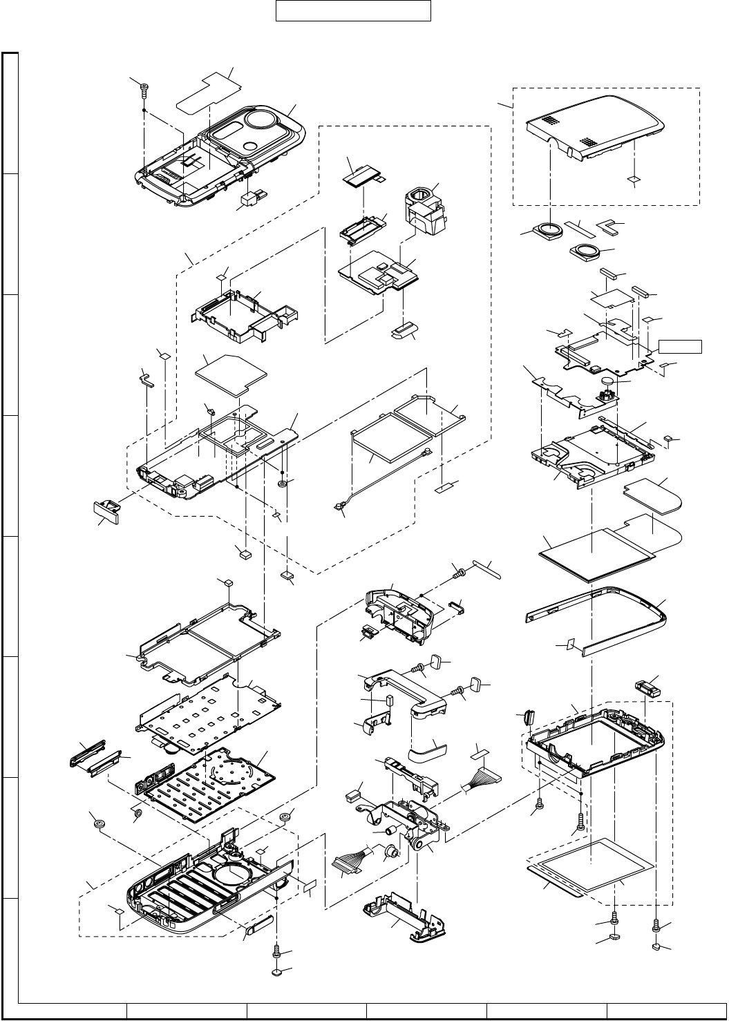
902SH
3
CONFIDENTIAL
[3] CABINET PARTS
A
B
C
D
E
F
G
H
12345 6
106-1
606x2
164
106-11
(PWB-H)
107
(PWB-E)
125
106-10
(LCD2000)
106-3
106-2
106-12
603x2
106-9
152
131
144
106-6
106-5
106-4
106-8
111
133
134
126
116
120
141
103-1
103
155
(MIC200)
103-1(*)
167
166
165
605x2
113x2
109
127
135
130
124
140
123
604
604
118
118
110
145
132
161
128
163
115
106-7x2
162
114
SD PWB-C
PWB-B
MAIN PWB-A
101-1
601x2
604x2
147
101
119
157
(EP1000)
154
(LCD3000)
129
122
151
139
108
(PWB-F)
153
(BAT1200)
117
602
112 112
602
159
(PWB-G)
142
143
137
102
102-1
102-1, 103-1(*): Deleted in the middle of October production.
139: Deleted in the December production.
138
136
158
(SP2000) 158
(SP2001)
137
149
150
160
(PWB-D)
104
106
156 (VIB001)
106-13x2
155
(MIC201)

902SH
4
CONFIDENTIAL
NO. PARTS CODE PRICE
RANK
NEW
MARK
PART
RANK DESCRIPTION
[3] CABINET PARTS
101 DCABAW169AFSE BB Front Cabinet (Display) Assembly
101- 1 GMADIA049AFSA AK Panel,Main Display
102 DCABBW169AFSC AY Back Cabinet (Display) Assembly [C]
102 DCABBW169AFSE AY Back Cabinet (Display) Assembly(Except for C,F,K,U
102 DCABBW169AFSF AY Back Cabinet (Display) Assembly [F]
102 DCABBW169AFSK AY Back Cabinet (Display) Assembly [K]
102 DCABBW169AFSU AY Back Cabinet (Display) Assembly [U]
102- 1 TLABZ2595AFZZ AA Sensor Moisture (Large)
103 DCABCW169AFSC AY Front Cabinet (Key) Assembly [C]
103 DCABCW169AFSE AY Front Cabinet (Key) Assembly (Except for C,F,K,U)
103 DCABCW169AFSF AY Front Cabinet (Key) Assembly [F]
103 DCABCW169AFSK AY Front Cabinet (Key) Assembly [K]
103 DCABCW169AFSU AY Front Cabinet (Key) Assembly [U]
103- 1 TLABZ2783AFZZ AA Sensor,Moisture (Small)
104 DCABDW169AFSE BD Back Cabinet (Key) Assembly
106 DKENDW169AFSB Board Unit [B]
106 DKENDW169AFSC Board Unit [C]
106 DKENDW169AFSD Board Unit [D]
106 DKENDW169AFSE Board Unit [E]
106 DKENDW169AFSF Board Unit [F]
106 DKENDW169AFSG Board Unit [G]
106 DKENDW169AFSH Board Unit [H]
106 DKENDW169AFSK CZ Board Unit [K]
106 DKENDW169AFSP Board Unit [P]
106 DKENDW169AFSR CZ Board Unit [R]
106 DKENDW169AFSS Board Unit [S]
106 DKENDW169AFST Board Unit [T]
106 DKENDW169AFSU Board Unit [U]
106 DKENDW169AFSW Board Unit [W]
106 DKENDW169AFSZ CZ Board Unit [Z]
106 DKENDW169AFS7 Board Unit [EP]
106 DKENDW169AFS8 Board Unit [GP]
106 DKENDW169AFS9 Board Unit [PP]
106- 1 DUNTKW169AFS1 BZ Camera Assembly
106- 2 LHLDFA006AF01 AG Holder,SD PWB
106- 3 LHLDZA091AF01 AH Holder Unit,Sub Display
!
106- 4 PSLDMA059AFZZ AF Cover,BBK Shield Case
!
106- 5 PSLDMA061AFZZ AK Cover,BBS Shield Case
!
106- 6 PSLDMA068AFZZ AH Cover,RF Shield Case
106- 7 QCNTAA017AFZZN AD Spacer,Hinge
106- 8 QCNWNA009AFZZ AN Coaxial,Cable
106- 9 QTANZA001AFZZL AB Contact,Spring
106-10 RLCUBA016AFZZ AW Sub Display (LCD2000)
106-11 RUITKA006AFZZ AS SD P.W.B. Connect FPC (PWB-H)
106-12 TLABZ2783AFZZ AA Sensor,Moisture (Small)
106-13 PSPAZA035AFZZ AA Spacer,CSP
107 CUITKA007AFZZ BB Key FPC Unit (PWB-E)
108 CUITKA009AFZZ AT LED FPC Unit (PWB-F)
109 GCABEA045AFSB AL Front Cabinet,Hinge
110 GCABFA045AFSB AL Back Cabinet,Hinge
111 GCOVAA058AFSD AD Screw Cover,Side
112 GCOVAA086AFSB AC Screw Cover,Display (Top)
113 GCOVAA089AFSB AC Screw Cover,Key (Top)
114 GCOVAA092AFSB AD Cover,External Connector
115 GCOVAA093AFSB AD Connector Cover,VIDEO OUT/Handsfree Microphone
116 GCOVAA094AFSB AH Slot Cover,Memory Card
117 GCOVAA134AFSA AE Screw Cover,Display (Bottom)
118 GCOVAA114AFSG AC Screw Cover,Hinge Cabinet
119 GCOVHA021AFSB AD Protect Cover,Cabinet
120 GCOVZA003AFSB AD Hinge,Memory Card Slot Cover
122 HDECQA023AFSB AN Belt,Top
123 HDECQA024AFSB AH Hinge Belt (Left)
124 HDECQA025AFSB AH Hinge Belt (Right)
125 JKNBZA046AFSA AV Button,10Key
126 LHLDFA005AFZZ AD Holder,Main PWB
127 LHLDWA006AFZZ AC Wire Holder,A
128 LHLDWA007AFZZ AC Wire Holder,B
129 LHLDZA090AF01 AR Holder Unit,Main Display
130 LHLDZA124AFZZ AC Fix Holder,Hinge
131 LHLDZA137AF01 AE Holder,Hinge
132 MHNG-A006AFZZ AY Hinge Unit
133 PCUSSA185AFZZ AB Cushion,Hinge
134 PCUSSA199AFZZ AA Cushion,Coaxial Cable
135 PCUSSA218AFZZ AC Cushion,Grease
136 PCUSSA230AFZZ AB Cushion,Connector
137 PCUSSA231AFZZ AB Cushion,Display PWB
138 PCUSSA232AFZZ AC Spacer Cushion,Back Cabinet (Display)
139 PCUSSA235AFZZ AB Cushion,LED FPC Unit
140 PMAGZA004AFZZ AE Magnet
141 PSHEGA003AFZZ AC Sheet,Side Keys
142 PSHEMA002AFZZ AC Leaf,Copper (With Glue)
143 PSHEMA004AFZZ AE Leaf,Copper (With Kapton)
144 PSHEZ1416AFZZ AB FPC Retainer Kapton
145 PSHEZA381AFZZ AB Kapton,Handling
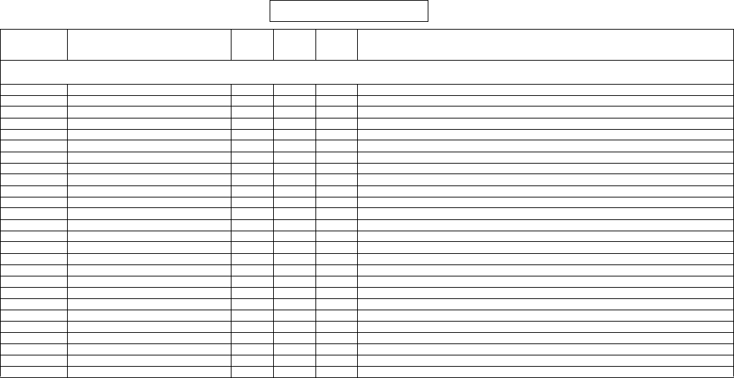
902SH
5
NO. PARTS CODE PRICE
RANK
NEW
MARK
PART
RANK DESCRIPTION
CONFIDENTIAL
147 PSHEZA388AFZZ AC Sheet,Top Belt
149 PSHEZA395AFZZ AB Sheet,Display PWB
150 PSHEZA396AFZZ AB Kapton,Display PWB
151 PSLDMA111AFZZ AG Sheet,Shield
152 PSPAZA037AFZZ AC Spacer,PWB
153 RDNTL0017AFZZ AG Battery,Back-up (BAT1200)
154 RLCUBA017AF02 BT Main Display (LCD3000)
155 RMICCA007AFZZ AK Microphone (MIC200,201)
156 RMOTVA004AFZZ AK Vibrator (VIB001)
157 RPHODA007AFZZ AK Earpiece (EP1000)
158 RSP-ZA009AFZZ AL Speaker (SP2000,2001)
159 RUITKA005AFZZ AP Speaker FPC (PWB-G)
160 RUITKA014AFZZ BB Sub Camera Unit (PWB-D)
161 RUITZA023AFZZ BC Thin Coaxial Cable
162 TLABZ2595AFZZ AA Sensor,Moisture (Large)
163 TLABZA075AF0T AC Label,Qualcomm
164 TSPC-A180AFZZ DH Label,Specifications
165 GCOVAA088AFSB AK Aerial Cover
166 GCOVAA090AFSA AC Cover,Infrared Port
167 GCOVZA004AFSB AD Cover,Strap
601 LX-EZ0184AFZZ AB Screw,M1.7x6mm
602 LX-EZ0193AFZZ AB Screw,M1.7x4.5mm,Black
603 LX-EZ0196AFZZ AB Screw,M1.7x5.5mm,Black
604 LX-EZA004AFZZ AB Screw,M1.4x2.8mm
605 LX-EZA010AFFN AB Screw,M1.7x7.5mm
606 LX-EZA011AFF7 AB Screw,M1.4x1.6mm
[3] CABINET PARTS
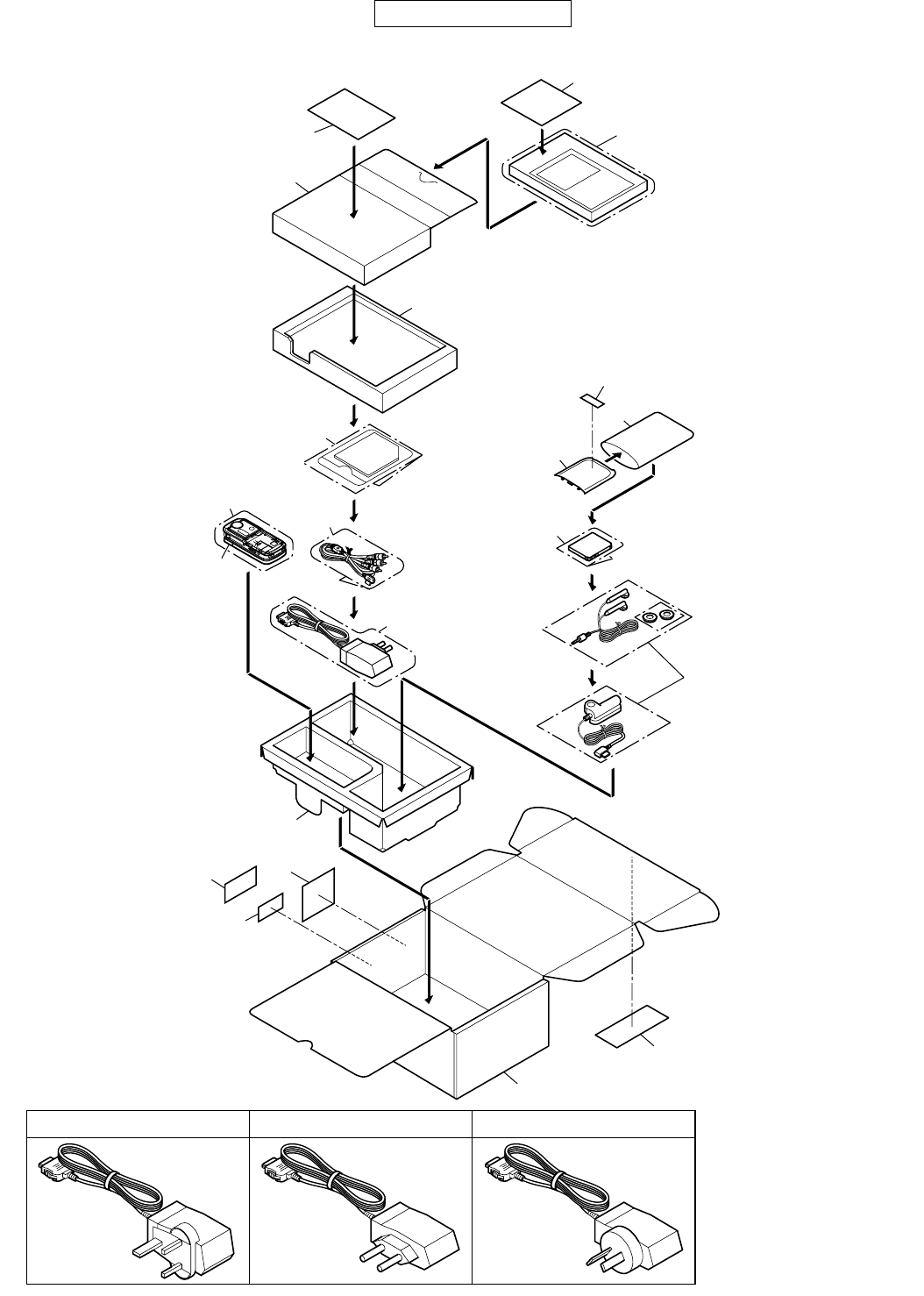
902SH
6
CONFIDENTIAL
[4] ACCESSORIES/PACKING PARTS
RADPTA010AF01
AC Charger
RADPTA009AF01 RADPTA011AF01
8
5
Phone
6
20 ([B,E,EP,D] Only)
21 ([G,GP,H] Only)
27
23 ([U] Only)
15 ([F] Only)
22 ([Z] Only)
29 ([B] Only)
2
7, 11,26
3
4
1
9
27 ([C,EP,F,K,U] Only)
12,14,16 ([T] Only),
17,18,19,30 ([B] Only)
25
10
24
13

902SH
7
CONFIDENTIAL
NO. PARTS CODE PRICE
RANK
NEW
MARK
PART
RANK DESCRIPTION
[4] ACCESSORIES/PACKING PARTS
1 GFTABA018AFSB AH Battery Cover (Except for [C,F,U])
1 GFTABA028AFSA AH Battery Cover [C,F,U]
2 QPLGJA005AFZZ AT Video Cable (Except for [C,F,U])
2 QPLGJA006AFZZ AT Video Cable [C,F,U]
!
3 RADPTA009AF01 ** AC Charger B,C,D,F,G,GP,H,K,P,PP,S,T,U,W(XN-1QC91)
!
3 RADPTA010AF01 ** AC Charger [E,EP,R] (XN-1QC90)
!
3 RADPTA011AF01 ** AC Charger [Z] (XN-1QC92)
4 RPHOHA004AF01 AY Handsfree Microphone Unit/Stereo Headset
5 SPAKAA026AFZZ AH Packing Add. [F,K]
5 SPAKAA046AFZZ AL Packing Add. [C,U]
5 SPAKAA051AFZZ AK Packing Add. [B,D,E,EP,G,GP,H,P,PP,R,S,T,W,Z]
6 SPAKCA172AFZZ AS Packing Case [B,D,E,P,PP,R,S,W,Z]
6 SPAKCA196AFZZ AS Packing Case [G,GP,H,T]
6 SPAKCA198AFZZ AN Packing Case [C,EP,F,K,U]
7 SPAKP1236AFZZ AA Polyethylene Bag,SD Memory Card
8 SPAKPA014AFZZ AC Polyethylene Bag,Phone
9 SPAKPA018AFZZ AN Accessories Box [B,D,E,EP,K,P,PP,R,S,W,Z]
9 SPAKPA019AFZZ AN Accessories Box [G,GP,H,T]
9 SPAKPA020AFZZ AN Accessories Box [F]
9 SPAKPA025AFZZ AR Accessories Box [C,U]
10 SPAKXA103AFZZ AG Pad,Division (Except for [C,U])
10 SPAKXA147AFZZ AL Pad,Division [C,U]
11 SSAKA0232AFZZ AC Case,SD Memory Card
12 SSAKAA004AFZZ AA Polyethylene Bag,User Guide (Except for [C,U])
12 SSAKA0022AFZZ AA Polyethylene Bag,User Guide [C,U]
13 SSAKH0329AFZZ AA Polyethylene Bag,Battery Cover
14 TCADHA039AFZZ AG Quick Start Guide [E,EP,R,Z]
14 TCADHA050AFZZ AK Quick Start Guide [G,GP]
14 TCADHA052AFZZ AM Quick Start Guide [T]
14 TCADHA054AFZZ AN Quick Start Guide [S]
14 TCADHA057AFZZ AN Quick Start Guide [D]
14 TCADHA059AFZZ AN Quick Start Guide [P,PP]
14 TCADHA061AFZZ AM Quick Start Guide [W]
14 TCADHA071AFZZ AS Quick Start Guide [H]
14 TCADHA103AFZZ Quick Start Guide [B]
15 TCAUHA013AFZZ AC Caution Label,Handsfree Microphone Unit ( [F]Only)
16 TCADZ0263AFZZ AC Card,Free Service ( [T] Only)
17 TCAUZA013AFZZ AB Caution Sheet,Video Cable
18 TGANEA016AFZZ AB Guarantee [E,EP]
18 TGANEA019AFZZ AE Guarantee [R]
18 TGANEA021AFZZ AE Guarantee [Z]
18 TGANGA005AFZZ AE Guarantee [K]
18 TGANIA004AFZZ AC Guarantee [T]
18 TGANSA001AFZZ AD Guarantee [S]
18 TGANZA033AFZZ AE Guarantee [D]
18 TGANZA035AFZZ AD Guarantee [P,PP]
18 TGANZA037AFZZ AC Guarantee [W]
18 TGANZA039AFZZ AE Guarantee [H]
18 TGANZA041AFZZ AD Guarantee [C]
18 TGANZA042AFZZ AF Guarantee [U]
19 TINSEA037AFZZ AM User Guide [E,EP,R]
19 TINSEA045AFZZ AY User Guide [Z]
19 TINSEA049AFZZ AP User Guide [C (English)]
19 TINSEA050AFZZ AY User Guide [U (English)]
19 TINSFA017AFZZ AM User Guide [F]
19 TINSFA019AFZZ AY User Guide [U (French)]
19 TINSFA027AFZZ AP User Guide [C (French)]
19 TINSGA013AFZZ AP User Guide [G,GP]
19 TINSGA016AFZZ AY User Guide [K]
19 TINSGA024AFZZ AP User Guide [C (German)]
19 TINSHA014AFZZ AY User Guide [H]
19 TINSHA028AFZZ AY User Guide [U (Dutch)]
19 TINSIA011AFZZ AS User Guide [T]
19 TINSIA015AFZZ AP User Guide [C (Italian)]
19 TINSPA023AFZZ AT User Guide [P,PP]
19 TINSSA012AFZZ AT User Guide [S]
19 TINSWA026AFZZ AS User Guide [W]
19 TINSZA018AFZZ AT User Guide [D]
19 TINSZA040AFZZ User Guide [B]
20 TLABZ2793AFZZ AA Sheet,Security ( [B,E,EP,D] Only)
21 TLABZA044AFZZ AC Sheet,Transparent ( [G,GP,H]Only)
22 TLABZA053AFZZ AB Label,ATIC ( [Z] Only)
23 TLABZA061AFZZ AC Label,Battery ( [U] Only)
!
24 UBATIA013AF01 ** Lithium Ion Battery (XN-1BT90)
25 UDSKAA017AF01 AL CD-ROM [B,D,E,EP,P,PP,R,S,W,Z]
25 UDSKAA023AF01 AL CD-ROM [G,GP,H,T]
25 UDSKAA024AF01 AL CD-ROM [C,F,K,U]
26 UIMC-A005AFZZ BF SD Memory Card (Except for [C,F,U])
26 UIMC-A006AFZZ BF SD Memory Card [C,F,U]
27 -------- - Label,Bar Code
29 TLABZA079AFZZ Label,Hungary ( [B] Only)
30 TCADZA066AFZZ DOC Copy ( [B] Only)

902SH
8
NO. PARTS CODE PRICE
RANK
NEW
MARK
PART
RANK DESCRIPTION
CONFIDENTIAL
[5] P.W.B. ASSEMBLY
!
PWB-B/
DDHAIZW169AFSE CA Display/Sub Camera Unit
PWB-E CUITKA007AFZZ BB Key FPC Unit
PWB-F CUITKA009AFZZ AT LED FPC Unit
PWB-G RUITKA005AFZZ AP Speaker FPC
PWB-H RUITKA006AFZZ AS SD P.W.B. Connect FPC
[6] OTHER SERVICE PARTS
PCOVPA003AFZZ AD Cap,Connector

902SH
9
CONFIDENTIAL
INDEX
– MEMO –

SHARP CORPORATION
Communication Systems Group
Quality & Reliability Control Centre
Higashihiroshima, Hiroshima 739-0192, Japan
No part of this publication may be reproduced,
stored in a retrieval system, or transmitted in
any form or by any means, electronic, mechanical,
photocopying, recording, or otherwise, without
prior written permission of the publisher.
COPYRIGHT 2004 BY SHARP CORPORATION
ALL RIGHTS RESERVED.
©
A0412-PDF KS KJ J
902SH CONFIDENTIAL
