Maxon Electronics Australia MM-5100P Maxon Australia 1X CDMA Voice/Data Modem User Manual 370575
Maxon Electronics Australia Pty. Ltd. Maxon Australia 1X CDMA Voice/Data Modem 370575
Contents
- 1. users manual
- 2. users manual 2
users manual 2

FCC Documentation
1/25
Maxon Proprietary : Restricted Distribution. This document is the sole and exclusive property of Maxon
Australia. Not to be distributed or divulged without prior written agreement.
Maxon Electronics Australia Pty. Ltd. 36A Gibson Avenue, Padstow, N.S.W. Australia
Tel : +61 2 9707-2000 Facsimile : +61 2 9707-3328 URL : http//www.maxon.com.au
User Manual
CM-5100P CDMA 1X Network card
Incorporating extracts of MM-5100P User Manual
Version : 0.1
Date : JUL. 25, 2003

FCC Documentation- CM-5100P CDMA 1X Network card
2/25
Maxon Proprietary : Restricted Distribution. This document is the sole and exclusive property of Maxon
Australia. Not to be distributed or divulged without prior written agreement.
Maxon Electronics Australia Pty. Ltd. 36A Gibson Avenue, Padstow, N.S.W. Australia
Tel : +61 2 9707-2000 Facsimile : +61 2 9707-3328 URL : http//www.maxon.com.au
FCC RF EXPOSURE COMPLIANCE
In August 1996 the Federal Communications Commission (FCC) of the United States with its action in Report
and Order FCC 96-326 adopted an updated safety standard for human exposure to radio frequency (RF)
electromagnetic energy emitted by FCC regulated transmitters. Those guidelines are consistent with the
safety standard previously set by both U.S. and international standards bodies. The design of this phone
complies with the FCC guidelines and these international standards.
Use only the supplied or an approved antenna. Unauthorized antennas, modifications, or attachments could
impair call quality, damage the phone, or result in violation of FCC regulations.
This CDMA PCMCIA Card has been tested for FCC RF exposure hand and body SAR compliance with
the MM-5100P PCMCIA Card form factor. In order to comply with FCC RF exposure requirements, the
CDMA PCMCIA Card module must be operated with the MM-5100P PCMCIA Card form factor. The use
of this device in any other type of host configuration may not comply with FCC RF exposure
requirements and should be avoided. During operation, a 1.5cm separation distance should be
maintained between the antenna, whether extended or retracted, and the user’s/bystander’s body
(excluding hands, wrists, feet, and ankles) to ensure FCC RF exposure compliance.
CAUTION
Change or modification without the express consent of Maxon Electronics Australia Pty. Ltd. voids the user’s
authority to use the equipment. This equipment has been tested and found to comply with the limits pursuant
to Part 15.105 of the FCC rules. These limits are designed to provide reasonable protection against harmful
interference in an appropriate installation. This equipment generates, uses, and can radiate radio frequency
energy and, if not used in accordance with instructions, can cause harmful radiation to radio communication.
However, there is no guarantee that interference will not occur in a particular installation. If the equipment
does cause harmful interference in radio and television reception, which can be determined by turning the
equipment on and off, the user is encouraged to try to correct the interference by one or more of the following
measures:
z Reorient or relocate the receiving antenna
z Increase the separation distance between the equipment and the receiver
z Contact Maxon Electronics Australia Pty. Ltd. Technical Support for assistance.

FCC Documentation- CM-5100P CDMA 1X Network card
3/25
Maxon Proprietary : Restricted Distribution. This document is the sole and exclusive property of Maxon
Australia. Not to be distributed or divulged without prior written agreement.
Maxon Electronics Australia Pty. Ltd. 36A Gibson Avenue, Padstow, N.S.W. Australia
Tel : +61 2 9707-2000 Facsimile : +61 2 9707-3328 URL : http//www.maxon.com.au
Table of contents
1. Contact Information······························································································· 4
2. Product Overview ·································································································· 5
2.1 Overview........................................................................................................ 5
2.2 What is the CM-5100P CDMA network card ............................................... 5
2.3 Supplied accessories................................................................................... 5
3. Specifications ········································································································ 6
3.1 Mechanical Specifications........................................................................... 6
3.2 Environment Specifications ........................................................................ 6
3.3 Electrical Specifications .............................................................................. 6
3.4 CDMA RF Specifications.............................................................................. 7
4. Instruction ·············································································································· 9
4.1 Supplied accessories................................................................................... 9
4.2 Getting started .............................................................................................. 9
5. Circuit description ······························································································· 14
5.1 CM-5100P CDMA 1X Network card circuit description ........................... 14
5.2 Power interface part ................................................................................... 15
5.3 Digital part................................................................................................... 15
5.4 RF part ......................................................................................................... 16
6. Range of operating power levels and description of means for variation of
operating power··································································································· 20
7. Description of frequency determining and stabilizing circuitry······················ 21
8. Description of circuit employed for suppression of spurious radiation ········ 23
9. Description of modulation system used ··························································· 24

FCC Documentation- CM-5100P CDMA 1X Network card
4/25
Maxon Proprietary : Restricted Distribution. This document is the sole and exclusive property of Maxon
Australia. Not to be distributed or divulged without prior written agreement.
Maxon Electronics Australia Pty. Ltd. 36A Gibson Avenue, Padstow, N.S.W. Australia
Tel : +61 2 9707-2000 Facsimile : +61 2 9707-3328 URL : http//www.maxon.com.au
1. Contact Information
If you have any technical queries about this manual, please contact:
Maxon Electronics Australia Pty. Ltd.
36a Gibson Avenue
Padstow, New South Wales 2211
Australia
Phone: +61 2 9707 2000
Fax: +61 2 9707 3328
Mr. Ray Sanders-Managing Director
Mr. Ashween Prasad- Technical Manager
Email: engineering@maxon.com.au

FCC Documentation- CM-5100P CDMA 1X Network card
5/25
Maxon Proprietary : Restricted Distribution. This document is the sole and exclusive property of Maxon
Australia. Not to be distributed or divulged without prior written agreement.
Maxon Electronics Australia Pty. Ltd. 36A Gibson Avenue, Padstow, N.S.W. Australia
Tel : +61 2 9707-2000 Facsimile : +61 2 9707-3328 URL : http//www.maxon.com.au
2. Product Overview
2.1 Overview
The CM-5100P wireless network card fits into a standard type 2 PC card slot (available on most
notebook PCs). This card functions as a wireless network card, a modem, a mobile phone and
allows you to connect to the Internet, send and receive e-mail, connect to a corporate network, and
make phone calls, without the need of a network cable or phone line.
The CM-5100P card performs data communication functions between Host and IS-95 CDMA Cellular
station.
2.2 What is the CM-5100P CDMA network card
- IS-95A, B, and cdma2000-1X CDMA Protocol Support
- Standard Type 2 PC card slot
- Remote controlled by AT commands
- DATA transmission up to 153Kbps [network limited]
- LED indicating of the modem status
2.3 Supplied accessories
- CM-5100P CDMA 1X network card (1)
- Ear-piece assembly (1)
- Driver CD (1)
FCC Documentation- CM-5100P CDMA 1X Network card
6/25
Maxon Proprietary : Restricted Distribution. This document is the sole and exclusive property of Maxon
Australia. Not to be distributed or divulged without prior written agreement.
Maxon Electronics Australia Pty. Ltd. 36A Gibson Avenue, Padstow, N.S.W. Australia
Tel : +61 2 9707-2000 Facsimile : +61 2 9707-3328 URL : http//www.maxon.com.au
3. Specifications
3.1 Mechanical Specifications
Table 3.1 mechanical specifications
Dimensions 95mm x 54mm x 5mm, except antenna parts
Weight Approx. 45g , except ear-piecd assemblies
Housing Material CASE – STAINLESS STEEL
3.2 Environment Specifications
Table 3.2 environment specifications
Operating conditions 0°C ~ +60°C , 85%(at 50(C), relative humidity (non-condensing)
Storage Temperature -40°C ~ +70°C
Humidity 95%, non-condensing
3.3 Electrical Specifications
Table 3.3 Current Consumption
- DC input voltage +5VDC from PCMCIA Slot
- Maximum current Under 1.0A
- Typical current Under 200mA
- Digital block operating voltage +3.0V (typical)
On communication @ Maximum TX Power (24+/- 0.3dBm) Under 700mA
(Note) The current consumption might vary of 5% over the whole operating temperature range.
FCC Documentation- CM-5100P CDMA 1X Network card
7/25
Maxon Proprietary : Restricted Distribution. This document is the sole and exclusive property of Maxon
Australia. Not to be distributed or divulged without prior written agreement.
Maxon Electronics Australia Pty. Ltd. 36A Gibson Avenue, Padstow, N.S.W. Australia
Tel : +61 2 9707-2000 Facsimile : +61 2 9707-3328 URL : http//www.maxon.com.au
3.4 CDMA RF Specifications
RF performances are compliant with IS-95A/B, cdma2000-1X RTT CDMA Protocol.
3.4.1 Transmitter specifications
Table 2.4 Transmitter performance
Type of Multiplexing Frequency-Division Duplex
Frequency Range 824.64MHz ~ 848.37MHz
Channel Number 20CH
Bandwidth 1.23MHz
Occupied Bandwidth Under 1.32MHz
Type of Oscillation PLL Synthesizer & VCTCXO(19.2MHz)
VCO Output Frequency Range
( divide-by-2 frequency range)
1372.08MHz ~ 1421.54MHz
(686.04MHz ~ 710.77MHz)
Intermediate Center Frequency 138.6MHz
Modulation Method OQPSK
RF Maximum Output Power 0.28W (24.5dBm/1.23MHz)
Frequency Stability(Accuracy) Under defined freq. +/- 300Hz
Waveform Quality Over 0.944
Conducted Spurious Emission Over carrier +/-900KHz, -42dBc/30KHz
Over carrier +/-1980KHz, -54dBc/30KHz
Common RF Impedance 50ohm
Supplied voltage +3.8V DC @ Power Amp.
+2.85V DC @ TX block
FCC Documentation- CM-5100P CDMA 1X Network card
8/25
Maxon Proprietary : Restricted Distribution. This document is the sole and exclusive property of Maxon
Australia. Not to be distributed or divulged without prior written agreement.
Maxon Electronics Australia Pty. Ltd. 36A Gibson Avenue, Padstow, N.S.W. Australia
Tel : +61 2 9707-2000 Facsimile : +61 2 9707-3328 URL : http//www.maxon.com.au
3.4.2 Receiver specifications
Table 2.5 Receiver performance
Type of Receiving Super Heterodyne Method
Frequency Range 869.94MHz ~ 893.37MHz
Channel Number 20CH
Band width 1.23MHz
Type of Oscillation PLL Synthesizer & VCTCXO(19.2MHz)
VCO Output Frequency Range
( divide-by-2 frequency range)
1372.08MHz ~ 1419.54MHz
(686.04MHz ~ 709.77MHz)
Intermediate Center Frequency 183.6MHz
Modulation Method QPSK
Receiver Sensitivity Under -104dBm @FER=0.5%
Single Tone Desensitization
(-30dBm @FC +/-900KHz)
Under -101dBm @FER=1%
-43dBm Under -101dBm @FER=1%
-32dBm Under -90dBm @FER=1%
Inter-modulation
(Fc +/-900KHz&1.7MHz)
-21dBm Under -79dBm @FER=1%
Common RF Impedance 50ohm
Supplied voltage +3.0V DC
FCC Documentation- CM-5100P CDMA 1X Network card
9/25
Maxon Proprietary : Restricted Distribution. This document is the sole and exclusive property of Maxon
Australia. Not to be distributed or divulged without prior written agreement.
Maxon Electronics Australia Pty. Ltd. 36A Gibson Avenue, Padstow, N.S.W. Australia
Tel : +61 2 9707-2000 Facsimile : +61 2 9707-3328 URL : http//www.maxon.com.au
4. Instruction
Warning
• To prevent fire or shock hazard, do not expose the unit to rain or moisture.
• Do not drop the unit or give a shock to the unit, or it may cause a malfunction.
4.1 Supplied accessories
- CM-5100P CDMA 1X Network card with antenna (1)
- ear-piece assembly (1)
4.2 Getting started
Before you can begin using the CM-5100P CDMA 1X network card, you must:
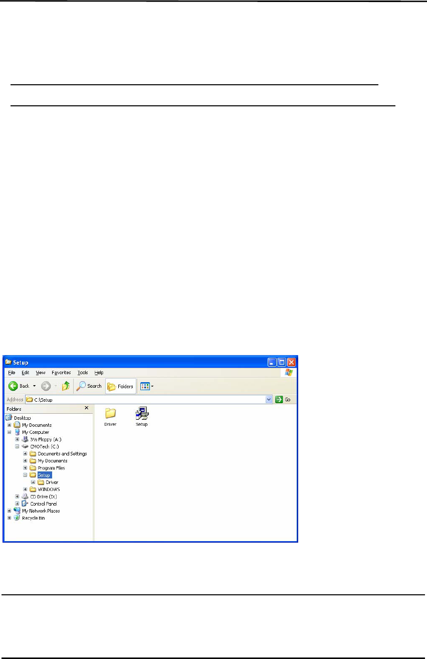
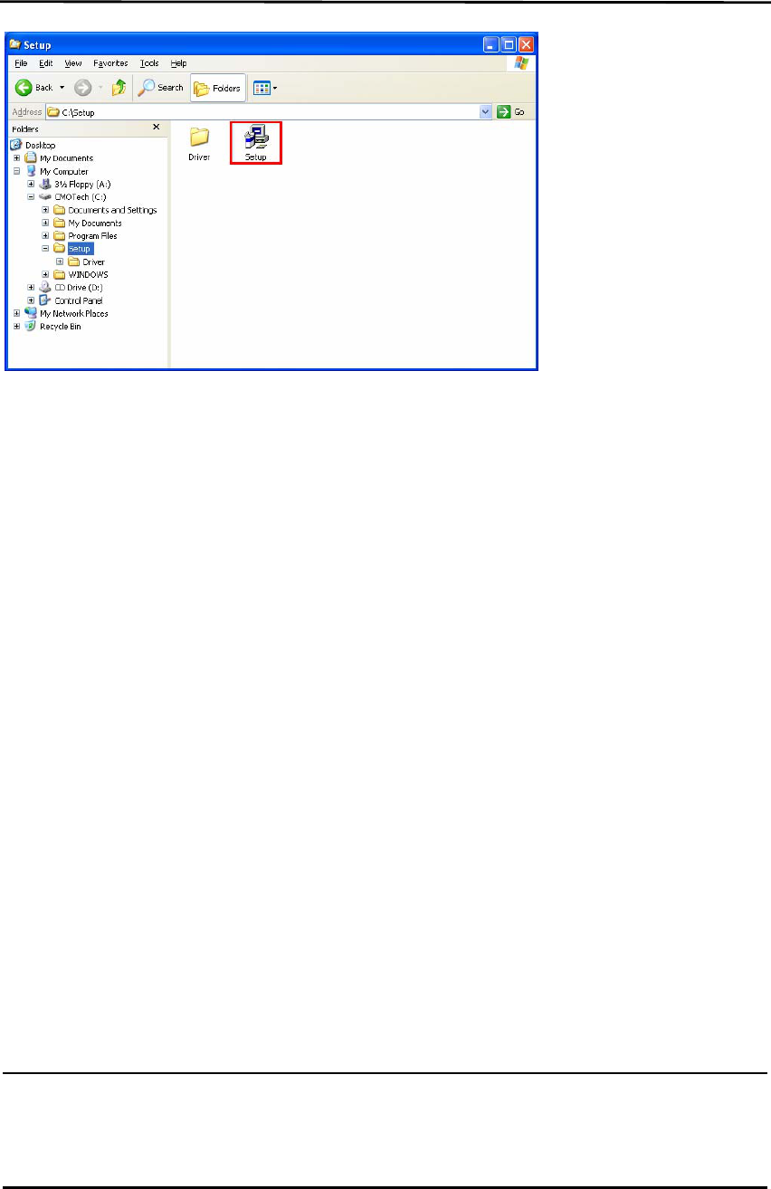
4.2.1 Install the driver software that forms the interface between the card and your Windows
operating system. Insert the CD into your CD-ROM drive.
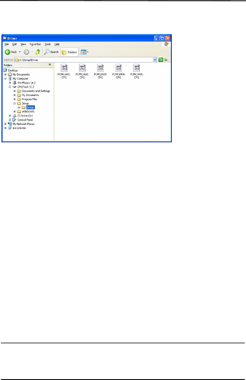
4.2.2 Compositions of Setup folder and files
FCC Documentation- CM-5100P CDMA 1X Network card
10/25
Maxon Proprietary : Restricted Distribution. This document is the sole and exclusive property of Maxon
Australia. Not to be distributed or divulged without prior written agreement.
Maxon Electronics Australia Pty. Ltd. 36A Gibson Avenue, Padstow, N.S.W. Australia
Tel : +61 2 9707-2000 Facsimile : +61 2 9707-3328 URL : http//www.maxon.com.au
4.2.3 Driver folder
4.2.4 Setup PCMCIA
Do not insert your PCMCIA card before execute the program of “Setup.exe”.
If you already insert your PCMCIA card to your PC, remove the your PCMCIA card and then double
click the icon of “Setup.exe”
Execute the Setup program
FCC Documentation- CM-5100P CDMA 1X Network card
11/25
Maxon Proprietary : Restricted Distribution. This document is the sole and exclusive property of Maxon
Australia. Not to be distributed or divulged without prior written agreement.
Maxon Electronics Australia Pty. Ltd. 36A Gibson Avenue, Padstow, N.S.W. Australia
Tel : +61 2 9707-2000 Facsimile : +61 2 9707-3328 URL : http//www.maxon.com.au
FCC Documentation- CM-5100P CDMA 1X Network card
12/25
Maxon Proprietary : Restricted Distribution. This document is the sole and exclusive property of Maxon
Australia. Not to be distributed or divulged without prior written agreement.
Maxon Electronics Australia Pty. Ltd. 36A Gibson Avenue, Padstow, N.S.W. Australia
Tel : +61 2 9707-2000 Facsimile : +61 2 9707-3328 URL : http//www.maxon.com.au
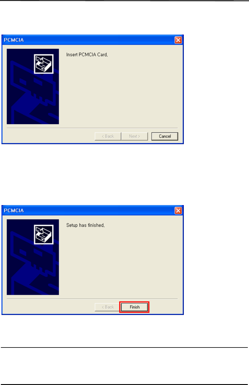
4.2.5 After execute “Setup.exe” insert your PCMCIA CDMA Network card
4.2.6 Setup complete
If you insert PCMCIA Network card, PC installs drivers and PCMCIA.
Click the button “Finish” and terminate the setup program.
FCC Documentation- CM-5100P CDMA 1X Network card
13/25
Maxon Proprietary : Restricted Distribution. This document is the sole and exclusive property of Maxon
Australia. Not to be distributed or divulged without prior written agreement.
Maxon Electronics Australia Pty. Ltd. 36A Gibson Avenue, Padstow, N.S.W. Australia
Tel : +61 2 9707-2000 Facsimile : +61 2 9707-3328 URL : http//www.maxon.com.au
4.2.7 Connect ear-piece to the ear-jack connector If you want to use as a phone.
Microphone and earphone signals for Voice Call are provided to interface with headset directly.
1. Connect the ear-piece plug firmly the ear-jack port hole.
2. Ware the Ear-piece to the left or right ear and adjust the ear-piece to fit to your ear firmly.
- Press for more than a second during buzzer ringing for receiving voice call
- Press for more than a second when redial, this time you heard dialing sound
When adjusting the volume on the unit, please refer to the “CM-5100P Software manual” for detail
information.
4.2.8 LED display
Table 4.2.1 LED function descriptions
LED Color
Function
RED GREEN YELLOW
Power Turn ON
Unsuccessfully Initialize
Ο
Successfully initialize & not enough to link Flashing
Successfully initialize & enough to link Ο
Voice call
Ο
Data connection & communication
Flashing
FCC Documentation- CM-5100P CDMA 1X Network card
14/25
Maxon Proprietary : Restricted Distribution. This document is the sole and exclusive property of Maxon
Australia. Not to be distributed or divulged without prior written agreement.
Maxon Electronics Australia Pty. Ltd. 36A Gibson Avenue, Padstow, N.S.W. Australia
Tel : +61 2 9707-2000 Facsimile : +61 2 9707-3328 URL : http//www.maxon.com.au
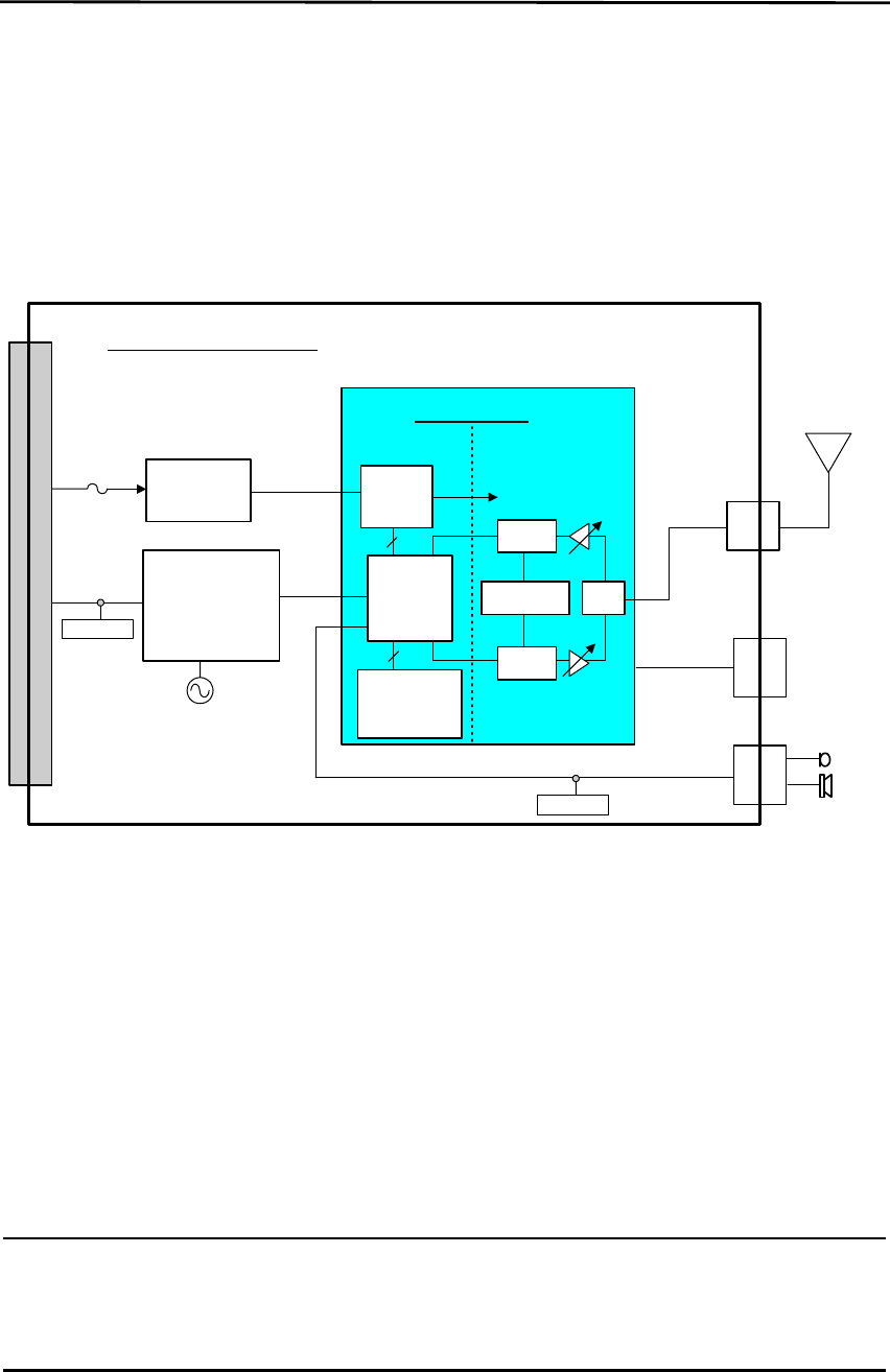
5. Circuit description
5.1 CM-5100P CMDA 1X Network card circuit description
The CM-5100P CDMA card consists of the CDMA Engine, power generation part, digital part, RF
part and connectors. The Fig 1-1 is block diagram of CM-5100P CDMA card.
Logic part
Rx
Tx
Synthesizer
RF part
LNA
Power
Amp
MSM5100
Memory
-Flash(32Mb)
-SRAM(08Mb)
Power
interface
LDO
Iout=1A
Vout=3.8V RF Vcc
Audio interface signal
Ear-jack
port
68pin PCMCIA
interface connector
CDMA Engine
CM-5100P Block Diagram
Fuse
protection
DUX
UART
with integrated
PCMCIA bus
interface
5V
protection
1.8432MHz
Debug Port
*only test
Figure 4.1 CM-5100P CDMA card block diagram

FCC Documentation- CM-5100P CDMA 1X Network card
15/25
Maxon Proprietary : Restricted Distribution. This document is the sole and exclusive property of Maxon
Australia. Not to be distributed or divulged without prior written agreement.
Maxon Electronics Australia Pty. Ltd. 36A Gibson Avenue, Padstow, N.S.W. Australia
Tel : +61 2 9707-2000 Facsimile : +61 2 9707-3328 URL : http//www.maxon.com.au
5.2 Power interface part
DC Power is supplied from PCMCIA card slot.
- LDO: This component is low dropout regulator. Output voltage is about 3.8V DC.
This LDO output voltage is inputted to CDMA Engine power interface.
Each block of CDMA Engine uses low-drop-output linear regulator.
- U500 : voltage regulator for digital circuit ( 2.8 DC )
- U501 : voltage regulator for VC-TCXO and IFR3300 ( 3.0V DC )
- U502 : voltage regulator for RF Rx part ( 3.0V DC )
- U503 : voltage regulator for RF Tx part ( 2.85V DC )
- U505 : voltage regulator for digital part(2.7V DC )
- And power AMP is directly supplied.
5.3 Digital part
- U400 : MSM(Mobile Station Modem) ASIC is chip responsible for CDMA/FM mobile station’s
base-band digital signal processing. For this chip to function, TCXO(19.2MHz) is required as
basic clocks.
And sleep crystal (32.768KHz) is used as clock source of MSM ASIC.
MSM consists of CDMA core and DFM core. CDMA core is a part for processing CDMA signal
consisting of modulator/demodulator, interleaver/deinterleaver and encoder/decoder in the CDMA
mode.
- U401: Memory part consists of Flash memory and SRAM.
Flash memory: store to main program.
SRAM: performs to read and write data
- U701:UART with integrated PCMCIA bus interface IC. For this chip to function, 14.7456MHz
is required as UART baud rate generator.

FCC Documentation- CM-5100P CDMA 1X Network card
16/25
Maxon Proprietary : Restricted Distribution. This document is the sole and exclusive property of Maxon
Australia. Not to be distributed or divulged without prior written agreement.
Maxon Electronics Australia Pty. Ltd. 36A Gibson Avenue, Padstow, N.S.W. Australia
Tel : +61 2 9707-2000 Facsimile : +61 2 9707-3328 URL : http//www.maxon.com.au
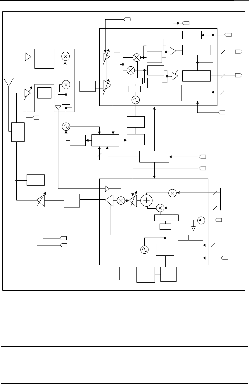
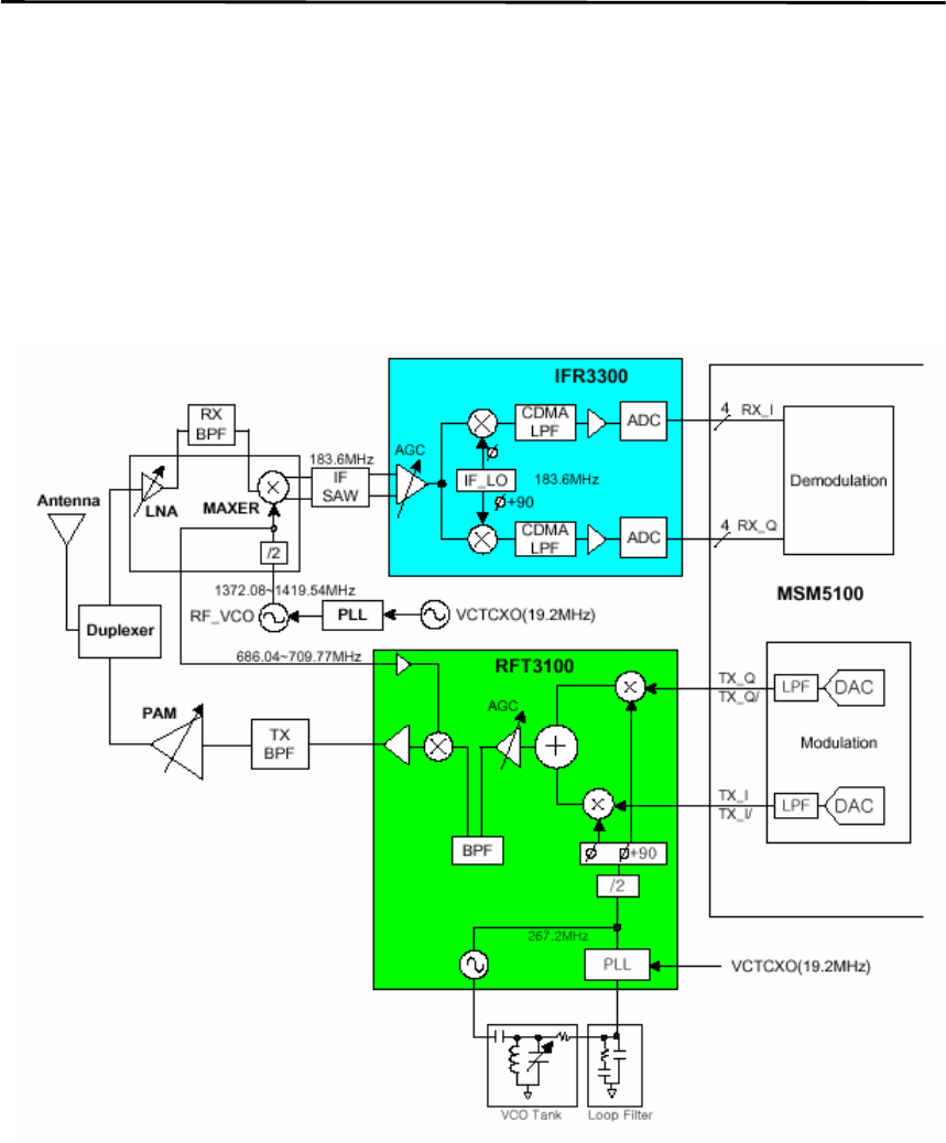
5.4 RF part
RF part consists of synthesizing part, transmission and reception part.
Fig 4.2 RF part block diagram
FCC Documentation- CM-5100P CDMA 1X Network card
17/25
Maxon Proprietary : Restricted Distribution. This document is the sole and exclusive property of Maxon
Australia. Not to be distributed or divulged without prior written agreement.
Maxon Electronics Australia Pty. Ltd. 36A Gibson Avenue, Padstow, N.S.W. Australia
Tel : +61 2 9707-2000 Facsimile : +61 2 9707-3328 URL : http//www.maxon.com.au
IF
SAW
LN A Mixer
S
W
0 90
F/2
CDMA
LPF
CDMA
LPF
GPS
LPF
GPS
LPF
G PS/CD M A
ADC
G PS/CD M A
ADC
ChipX8
ChipX8
TAN K
Circuit
1372.08~ 1419.54M H z
LOOP
Filte r
CDMA
Antenna
SBI &M O DE
CONTROL
LOGIC
PLL_CLK
PLL_DATA
PLL_EN
SBI
&M ODE
CONTROL
LOGIC
TX
BPF
LOOP
Filte r
HDET
VC TC XO
TX _A G C _A D J
183.6M H z
BPF
685~ 710M H z
PAM
R FT3100
367.2M H z
Pout= 24.5dB m
267.2M H z
Fc=138.6M H z
19.2M H z
4
4
2
2
TRK_LO _AD J
DUX : Duplexer
BPF : Band Pass Filte r
SAW : Surface Acoustic W ave
LN A : Low N oise A m plifier
PAM : Pow er Am plifier M odule
PLL: Phase-Lock Loop
VC O : Volta g e C o n tro lled O scillator
ADC: Analog to D igita l Converter
TX IL: 2.5dB
RX IL:4.0dB
T X a ttn : 4 0 d B
RX atten:55dB
IL: 3dB
IL: 12dB
IL : 3dB
DUAL
PLL
LOOP
Filte r
3
PLL
0 9 0
/2
R X _A G C _A D J
SBDT
SBCK
SBST
PA_O N
NF:1.2dB
Gain:16dB
N F :7 .0 d B
Gain:12dB
I&Q offset
RX_I DATA
RX_Q DATA
SBDT
SBCK
SBST
SLEEP
3
3
DAC_IREF
RX
BPF
/2
C X77105
TX_Q
TX_Q /
TX_I
TX_I/
LN A_G AIN
PA_O N
PA_R0
TAN K
Circuit
DUX

FCC Documentation- CM-5100P CDMA 1X Network card
18/25
Maxon Proprietary : Restricted Distribution. This document is the sole and exclusive property of Maxon
Australia. Not to be distributed or divulged without prior written agreement.
Maxon Electronics Australia Pty. Ltd. 36A Gibson Avenue, Padstow, N.S.W. Australia
Tel : +61 2 9707-2000 Facsimile : +61 2 9707-3328 URL : http//www.maxon.com.au
5.4.1.1 Frequency synthesizing part
Frequency synthesizing part called PLL Synthesizer consists of three synthesizer circuit which is first
local synthesizer, Tx IF synthesizer and Rx IF synthesizer. The first local synthesizer generates the
primary local system oscillation frequency, operating over 1372.08 ~ 1419.54 MHz frequency range.
Tx IF and Rx IF synthesizer generate the second local oscillation frequency, 267.2 MHz and 367.2
MHz respectively.
5.4.1.2 Receiving part
- Duplexer. The duplexer filters the RF signal transmitted through Antenna and sends the
signals to LNA.
- LNA. This part in front-end is used to amplify the received signal with low noise figure
- Down converter. It acts as a mixer using first local frequency to produce the desired signal
in the mid-range frequency of 183.6 MHz.
- Rx AGC. This part is designed to control the gain of the dynamic range of midrange
frequency produced in down converter according 80 dB dynamic range.
Currently, previous BBA is divided into IFR3300(Rx IF-baseband converter) and RFT3100(Tx
baseband-IF converter). IFR3300 acts as the baseband analog processor which processing the
signals between the IFR3300 and digital processing circuit.
In the while, RFT3100 consists of Tx AGC and Tx part analog processor of previous BBA.
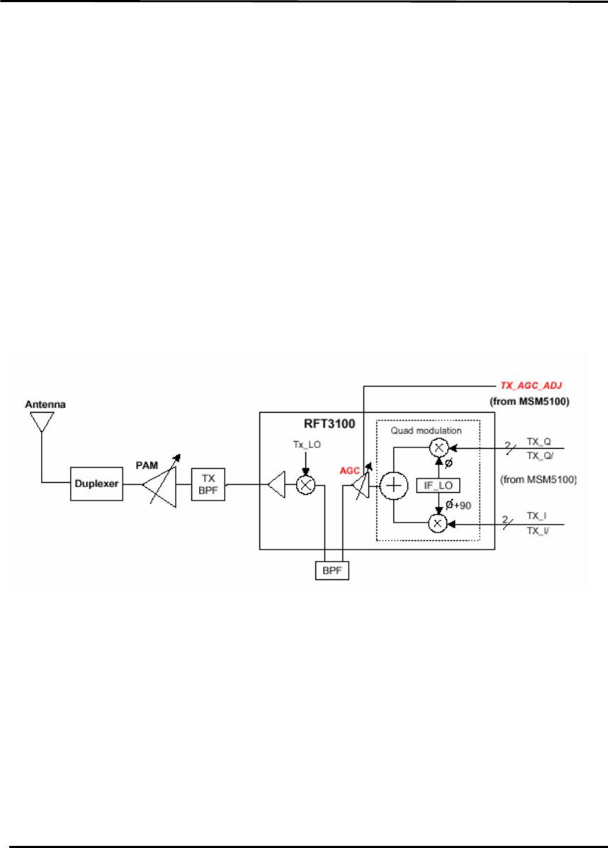
5.4.1.3 Transmission part
- Tx AGC. It is designed to be gain-controlled from 84 dB dynamic range. The gain of this part
is controlled by MSM using digital control signal.
- Up converter. This part mixes the IF transmission frequency 138.6 MHz and the first local
1372.08 ~ 1419.54 MHz to generate transmission frequency of 824.64 ~ 848.37 MHz.
- Power AMP module. This part is designed to work in 824 MHz ~ 849 MHz frequency range
in the CDMA mode and can generate the proper output power. The DC voltage into the power

FCC Documentation- CM-5100P CDMA 1X Network card
19/25
Maxon Proprietary : Restricted Distribution. This document is the sole and exclusive property of Maxon
Australia. Not to be distributed or divulged without prior written agreement.
Maxon Electronics Australia Pty. Ltd. 36A Gibson Avenue, Padstow, N.S.W. Australia
Tel : +61 2 9707-2000 Facsimile : +61 2 9707-3328 URL : http//www.maxon.com.au
amp module is typical 3.8V.
FCC Documentation
20/25
Maxon Proprietary : Restricted Distribution. This document is the sole and exclusive property of Maxon
Australia. Not to be distributed or divulged without prior written agreement.
Maxon Electronics Australia Pty. Ltd. 36A Gibson Avenue, Padstow, N.S.W. Australia
Tel : +61 2 9707-2000 Facsimile : +61 2 9707-3328 URL : http//www.maxon.com.au
6. Range of operating power levels and description of means for
variation of operating power
Dynamic range of output power is from –56dBm to +24.5dBm with ±0.3dB variation in CDMA mode.
A temperature-compensated TX AGC (Automatic Gain Control) amplifier with 85dB gain range is
included in the RFT3100. The transmit output power level is directly controlled by varying the gain of
this TX AGC amplifier. A DC input voltage from the MSM5100 linearly controls the gain of the TX
AGC amplifier.
The 84 dB dynamic range is 39 dB when the voltage 2.8V and -45 dB in 0.1V. The 81 dB dynamic
range (0.3V ~ 2.4V) gain is used in this CDMA card.

FCC Documentation
21/25
Maxon Proprietary : Restricted Distribution. This document is the sole and exclusive property of Maxon
Australia. Not to be distributed or divulged without prior written agreement.
Maxon Electronics Australia Pty. Ltd. 36A Gibson Avenue, Padstow, N.S.W. Australia
Tel : +61 2 9707-2000 Facsimile : +61 2 9707-3328 URL : http//www.maxon.com.au
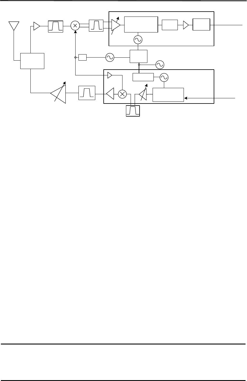
7. Description of frequency determining and stabilizing circuitry
Frequency synthesizing part is composed of the first local RX IF synthesizer which is single mode
PLL synthesizer and the internal Tx IF and Rx IF synthesizer which are in RFT3100 and IFR3300
chip. These parts generate the first local oscillation frequency, Rx IF frequency and Tx IF frequency.
- First local frequency Synthesizer : 1372.08 MHz ~ 1419.54 MHz
PLL loop is composed of single PLL synthesizer, Loop filter, VCO and VC-TCXO
It generates transmission and reception frequency of 9551372.08 MHz ~ 1419.54 MH
- Rx IF synthesizer : 367.2 MHz
Rx IF PLL loop is consisted of PLL synthesizer in the PLL module, VCO built in IFR3300, loop
filter and VC-TCXO(Crystal oscillator 19.2 MHz). It oscillates twice the intermediate receiving
frequency of 367.2 MHz and then generates 183.6 MHz, Rx IF frequency.
- Tx IF Synthesizer : 267.2 MHz
The configuration of PLL loop is composed of PLL Synthesizer, VCO which is internally installed,
loop filter and VC-TCXO(19.2 MHz). It oscillates twice of the transmission intermediate
frequency of 267.2 MHz and then generates Tx IF frequency of 138.6 MHz through the PLL loop.
The frequency of 19.2 MHz generated from the VC-TCXO is the main clock of each the frequency
synthesizer part. PLL frequency stability is determined by the stability of oscillator of VC-TCXO. This
prevents maximum frequency variation from exceeding ±2.0PPM.
FCC Documentation- CM-5100P CDMA 1X Network card
22/25
Maxon Proprietary : Restricted Distribution. This document is the sole and exclusive property of Maxon
Australia. Not to be distributed or divulged without prior written agreement.
Maxon Electronics Australia Pty. Ltd. 36A Gibson Avenue, Padstow, N.S.W. Australia
Tel : +61 2 9707-2000 Facsimile : +61 2 9707-3328 URL : http//www.maxon.com.au
Duplexer
VCO
LNA MAXER
1372.08~1419.54MHz
TX_I &Q
Dual
PLL
VCTCXO(19.2MHz)
183.6MHz
Antenna
AGC
RFT3100
267.2MHz
AGC
Quad
modulation
TX PLL
PAM
/2
Quad
Demodulation
I&Q
LPFs ADCs
RX I&Q Data
367.2MHz

FCC Documentation Feb. 12, 2003
23/25
Maxon Proprietary : Restricted Distribution. This document is the sole and exclusive property of Maxon
Australia. Not to be distributed or divulged without prior written agreement.
Maxon Electronics Australia Pty. Ltd. 36A Gibson Avenue, Padstow, N.S.W. Australia
Tel : +61 2 9707-2000 Facsimile : +61 2 9707-3328 URL : http//www.maxon.com.au
8. Description of circuit employed for suppression of spurious
radiation
In the CDMA transmit signal path, the frequency spectrum at the output of the CDMA DACs contains
unwanted frequency components due to the DAC output transition edges and transients. The
transmit clock frequency and harmonics are found in the spectrum.
Each CDMA DAC is followed by an anti-aliasing low-pass filter with a bandwidth of 630 KHz that
reduces unwanted frequency components installed in MSM5100. And then Tx IF frequency from the
RFT3100 is filtered by bandpass filter. The nominal specification of the filter is as following.
- Nominal center frequency : 138.6 MHz
- 3 dB Bandwidth : ± 630 kHz
- Stop band attenuation : 40dB min.
The Tx RF output of the Tx Mixer and the AGC amp is filtered again by the SAW band pass filter.
The nominal specification of the filter is as follows.
- Pass band : 824 MHz ~ 869 MHz
- Attenuation : DC ~ 800MHz : 22 dB min.
869 MHz ~ 1049 MHz : 25 dB min.
1049 MHz ~ 2000 MHz : 19 dB min.
Finally, the spurious generated from Power AMP is filtered by the duplexer. The nominal specification
of the duplexer is as follows
- TX Pass band : 824 MHz ~ 869 MHz
- Attenuation : 869 MHz ~ 894 MHz : 40 dB min.
FCC Documentation Feb. 12, 2003
24/25
Maxon Proprietary : Restricted Distribution. This document is the sole and exclusive property of Maxon
Australia. Not to be distributed or divulged without prior written agreement.
Maxon Electronics Australia Pty. Ltd. 36A Gibson Avenue, Padstow, N.S.W. Australia
Tel : +61 2 9707-2000 Facsimile : +61 2 9707-3328 URL : http//www.maxon.com.au
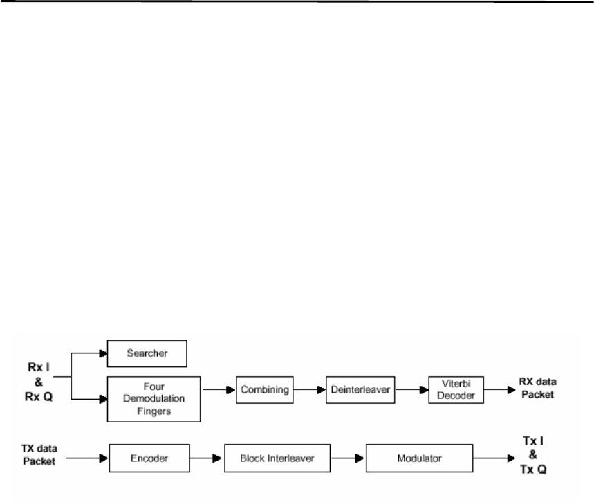
9. Description of modulation system used
The CM-5100P CDMA card consists of MSM, baseband analog interface (RFT31000, IFR3300) as
modulation system. The MSM integrates functions of a CDMA processing, a digital FM(DFM)
processing, CDMA subsystem in the MSM performs CDMA signal processing about CDMA
modulation / demodulation, viterbi coding/decoding, interleaving/de-interleaving, and etc.
The CDMA baseband processor performs forward-link demodulation, time tracking and reverse-link
modulation for CDMA digital signals. The following figure shows a CDMA digital baseband processor
block diagram.
Figure 8-1 CDMA digital Baseband Block Diagram
The modulator performs the orthogonal modulation, long code PN spreading and quadrature
spreading. The resulting data stream is then band limited with FIR filters and sent to the analog
baseband processor.
The RFT3100 Transmit Signal Path (shown in figure 8-2) accepts analog I and Q data from the MSM
and outputs modulated IF centered at 138.6 MHz to the RF transmitter. The RFT3100 transmit path
outputs a differential IF signal with spread spectrum modulation expending ±630KHz from the
transmit IF center frequency of 138.6 MHz.
The analog I and Q baseband components from the CDMA low-pass filters are mixed in quadrature
with unmodulated I and Q signals at 138.6 MHz. After mixing, the I and Q IF components are
summed and output differentially. The 138.6 MHz I and Q IF VCO signals are generated on the
FCC Documentation Feb. 12, 2003
25/25
Maxon Proprietary : Restricted Distribution. This document is the sole and exclusive property of Maxon
Australia. Not to be distributed or divulged without prior written agreement.
Maxon Electronics Australia Pty. Ltd. 36A Gibson Avenue, Padstow, N.S.W. Australia
Tel : +61 2 9707-2000 Facsimile : +61 2 9707-3328 URL : http//www.maxon.com.au
RFT3100.
The transmitter IF VCO is set to 267.2 MHz by an external varactor-tuned resonant tank circuit. An
internal phase-lock loop and external loop filter network provides the feedback to the varactor that
tune the VCO precisely to 267.2 MHz. A master-slave divide-by-two circuit generates I and Q signals
in precise quadrature for the mixers.
Figure 8-2 IFR3300 and RFT3100 Functional Block Diagram