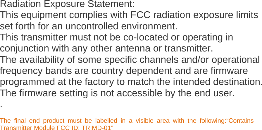
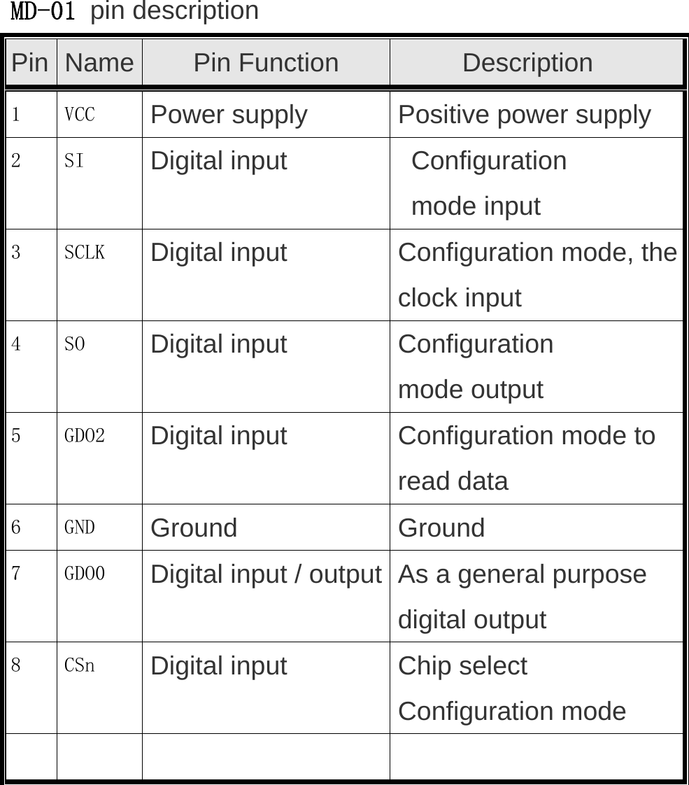
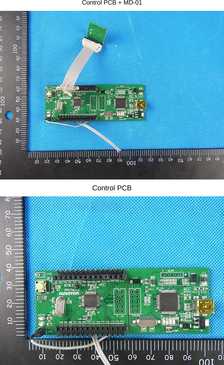
MEIJIAXIN TOYS MD-01 2.4G module User Manual
Meijiaxin Toys Co., Ltd. 2.4G module
UserManual.wiki
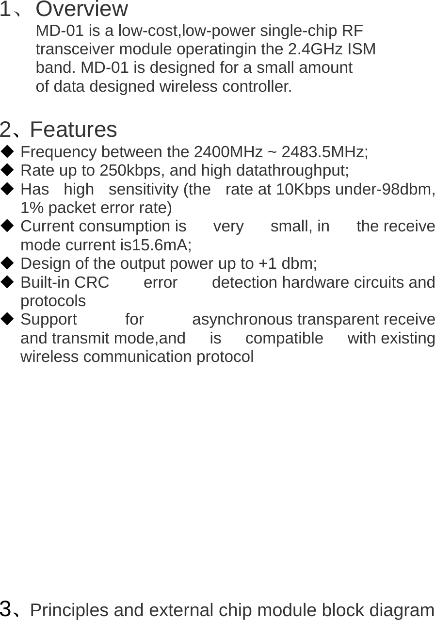
>
MEIJIAXIN TOYS
>
MD 01 User Manual
User manual
Navigation menu
Upload a User Manual
Namespaces
Wiki Guide
HTML
PDF
Info
Views
User Manual
Discussion / Help
Navigation