Metering Technology RFLAN RFLAN Module User Manual Operational Overview
Metering Technology Corporation RFLAN Module Operational Overview
Contents
- 1. User Manual
- 2. Assembly Instructions
User Manual

Tested and Report Prepared By: FCC ID: PDVRFLAN
ITC Engineering Services
9959Calaveras Road, Box 543
Sunol, CA 94586-0543
Tel: 925-862-2944 Fax: 925-862-9013
Email: docs@itcemc.com Web: www.itcemc.com
RF-LAN Module
User’s Guide v1.01
September 23, 2002

RF-LAN User’s Guide v1.01 -- Confidential – FCC ID: PDVRFLAN
2002 Metering Technology Corporation. All Rights Reserved Page 2
FCC WARNING STATEMENTS
Note: This equipment has been tested and found to comply with the limits for a Class B digital
device, pursuant to Part 15 of the FCC.
Rules: These limits are designed to provide reasonable protection against harmful interference in
a residential/office installation. The equipment generates, uses, and can radiate radio frequency
energy, and if not installed and used in accordance with the instructions, may cause harmful
interference to radio communications. However, there is no guarantee that interference will not
occur in a particular installation. If this equipment does cause harmful interference to radio or
television reception, which can be determined by turning the equipment off and on, the user is
encouraged to try to correct the interference by one or more of the following measures:
• Reorient or relocate the receiving antenna.
• Increase the separation between the equipment and receiver.
• Connect the equipment into an outlet on a circuit different from that to which the receiver is
connected.
• Consult the dealer or an experienced Radio/TV technician for help.
CAUTION: Changes or modifications not expressly approved by the party responsible for
compliance could void the user’s authority to operate the equipment.
FCC LABEL STATEMENT
This device complies with FCC Rules Part 15. Operation is subject to the following two conditions:
(1) This device may not cause harmful interference and (2) This device must accept any interference
that maybe received, including interference that may cause undesired operation.
INSTRUCTIONS TO THE INSTALLER & USER
Minimum Safe Distance: 0.14943 meters (5.9 inches)
Antenna Substitution: Do not substitute any antenna for for the one supplied by the
manufacturer. You may be exposing person(s) to harmful
radiation. Contact supplier or the manufacturer for further
instructions.
Table of Contents
Operational Overview ...............................................................................................................................4
Electrical Specifications............................................................................................................................4
Hardware Description ...............................................................................................................................5
Software Description.................................................................................................................................6
Commands To RF LAN Card: ..............................................................................................................7
Connector Details......................................................................................................................................7
J1 Connector .........................................................................................................................................7
J2 Connector .........................................................................................................................................8
J3 Connector .........................................................................................................................................8
FCC ID: PDVRFLAN
RF-LAN User’s Guide v1.01 -- Confidential – FCC ID: PDVRFLAN
2002 Metering Technology Corporation. All Rights Reserved Page 4
Operational Overview
The purpose of the RF-LAN Module is to provide communication over the air to another similar unit
or an RF-LAN Hub. The RF-LAN Module can be installed in different types of host electronic
measurement, control, and data acquisition equipment, such as electric meters.
The following describes the general operation of the RF-LAN Module:
• The Module operates in ISM band (902 – 928 MHz) using the Frequency Hopping method.
• The Module can be installed in devices that provide a 5VDC power supply.
• Communication with the host device is accomplished through a 9600 baud serial interface.
• The Module adjusts output RF power according to reception of an acknowledgment signal.
• The Module can communicate with a similar Module located in other devices, such as a
Gateway, and with low power RF transceivers located nearby inside devices like Water or
Gas Meters.
Electrical Specifications
Operating Voltage: 5VDC +/- 5%
Consumed Current : < 1A, peak
Effective Radiated Output RF Power with Tuned Antenna: 10, 15, 20, 25, 30 dBm,
programmable
Frequency Range: 902 – 928 MHz
Number of Channels: 50, minimum
Data Rate: 1200, 2400, 4800, 9600,
programmable
Receiver Sensitivity: -105dBm, maximum
Adjacent Channel Rejection: 45dBc, min
Out of Band Signal Rejection: 60dBc, min
Frequency Synthesizer Steps: 500Hz, max
RF Input/Output Impedance: 50 Ohm
Receiver Saturation: 126 dBuV/m, min
RF-LAN User’s Guide v1.01 -- Confidential – FCC ID: PDVRFLAN
2002 Metering Technology Corporation. All Rights Reserved Page 5
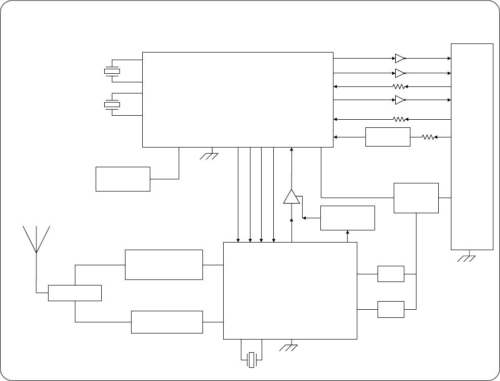
Hardware Description
The main building blocks of the RF-LAN Module are the microcontroller, the RF transceiver, and
the 1-Watt RF power amplifier, as shown in the following Figure 1: Block Diagram of RF-LAN
Module.
MSP430F149 Microcontroller
Connector
J1
to
Meter
RF Transceiver CHIPCON CC1000
Tx Path
1W PA
T/R Switch
Rx Path
LNA , SAW FILTER
and Glue Logic
Line Filter
and 3.3V
LDO
Data Control
Using RSSI
3.3V
Filter
3.3V
Filter
ENB
RF Tx in Progress
RFLAN Reset Status
RFLAN Tx Input
RFLAN Rx Output
RFLAN Reset Input
RFLAN Mode Input
VCC
5V
V
C
C
3
.
3
V
Analog Vcc
Digital Vcc
VCC 3.3V
CC1000
TX-OUT
C
C
1
0
0
0
-
A
L
E
C
C
1
0
0
0
-
P
C
L
K
C
C
1
0
0
0
-
P
D
A
T
A
32 KHz
11.059 MHz
Block Diagram Of Mesa Verde Project
4.0 MHz
Power ON
Reset IC
P
3
.
0
R
x
1
P
3
.
2
P
3
.
1
C
C
1
0
0
0
-
D
I
O
T
x
1
P2.0
P2.1
Rx0
Tx0
P1.7
/RST-NMI
XOUT/TCLK
XIN
XT2IN
XT2OUT
JTAG PORT
J2
VCC
Figure 1: Block Diagram of RF-LAN Module
J1 is the I/O connector to interface to the host device.
J2 is the MSP430 programming header.
The MSP430 controller is the heart of the circuit, which interfaces with the host device via the J1
port, and to the RF section through the CC1000 chip. The firmware program resides in the internal
flash of MSP430. MSP430 has two crystals, Y1 is 32.768 KHz and Y2 is 4.0MHz. Y1 is basically
used to work with a JTAG emulator for debug purposes, Y2 is used for normal operation. When the
RF LAN Module is connected to a host device, the host device controls the way the RF LAN
Module will work through the serial port, J1.5 (Reset), and J1.6 (Command/Data).
RF-LAN User’s Guide v1.01 -- Confidential – FCC ID: PDVRFLAN
2002 Metering Technology Corporation. All Rights Reserved Page 6
MSP430 controls all of the functions on the RF-LAN Module, it talks to the host device via Serial
port 0. The mode of RF-LAN is set by the signal level at J1.6. When the signal level is high it is in
command mode, when the signal level is low it is in data mode. MSP430 appropriately handles the
data by polling the J1.6.
MSP430 talks to the CC1000 via port bits and sends/receives RF data using serial port 1.
MSP430 initializes CC1000 by toggling port bits (simulated synchronous serial bus), P3.2 (PCLK),
P3.1 (PDATA IO), and P3.0 (PALE), as provided by the CC1000 data sheets.
The CC1000 is a single chip RF transceiver, used for wireless application in the ISM band 300-
1000MHz frequency ranges. The analog and digital supply to CC1000 is well filtered by using a PI
filter to suppress noise. An 11.059 MHz crystal is connected to CC1000 as a reference for the data
rate and for other internal functions.
On the receive path, the RF input signal from the antenna goes through a saw filter, an LNA, and a
50-ohm impedance matching network, before feeding the RF input of CC1000. Great care is taken
to design the traces on these paths to match for 50-ohm traces in order to reduce loss.
On the transmit path, the RF2131 IC is connected to the RF output of CC1000 to provide a 1-Watt
RF power output. The MSP430 controller does the on-off control of the PA.
The RF transmit and receive paths are connected to the antenna via a T/R switch. MSP430
controls which signal to pass by controlling the T/R switch, using port bits.
When CC1000 is programmed in receive mode, the data to the MSP430 is allowed only when
RSSI (Receiver Signal Strength Indicate) is better than –105 DBm, using RSSI signal and glue
logic.
MAX825SEUK (U5) provides the power on reset to the RF-LAN Module.
Software Description
At power-on, MSP430 initializes all port pins and initializes the CC1000. MSP430 sets the mode of
operations by looking at J1 connector mode input (J1.6). The host device initializes all the RF-LAN
registers at power-on in command mode.
When J1.6 is in data mode, MSP430 initializes the CC1000 in Rx mode. When a valid data packet
is received, MSP430 checks for the valid CRC. If valid, it checks to see if it is addressed to this RF-
LAN Module. If addressed correctly, the data packet is sent to the host device.
In data mode, data received on the serial port is buffered and packetized with the header,
initialized with the CC1000 in the transmit mode, setting the T/R switch to the transmit path, and
sends the data to the CC1000 to transmit the data over the air. Once the data is sent, the CC1000
is switched to the receive mode, waiting for the acknowledge packet for the data just sent. The
frequency-hopping algorithm is implemented to send/receive data on various frequency channels.
The frequency-hopping tables are residing in the flash of MSP430.
RF-LAN User’s Guide v1.01 -- Confidential – FCC ID: PDVRFLAN
2002 Metering Technology Corporation. All Rights Reserved Page 7
Commands To RF-LAN Module
The following are the commands between the host device and the RF-LAN Module.
Command Name Description
Reset Resets the RF-LAN Module firmware
Clear Reset Status Sets the Reset Status pin of the RF-LAN Module to a non-
default state
Sleep Puts the RF-LAN Module into low power mode
Wakeup Removes the RF-LAN Module from low power mode
Abort Tx Aborts any transmission in progress
Read Register Returns value of requested RF-LAN Module Register(s)
xxxx = # of bytes to read (xxxx = 0 is invalid)
Register # follows the command byte
Write Register Writes value(s) into requested RF-LAN Module Register(s)
xxxx = # of bytes to write (xxxx = 0 invalid)
Register # follows the command byte
SOH Reserved – Indicates start of message
Connector Details
J1 Connector
The J1 connector is designed so it can be used either as a 12 Pin 1x12 0.1” header or a 12
Position edge connector with a pitch of 0.1”. The signal definition is as follows.
Pin
#
Pin Name Pin Description MTC Signal
Direction
Voltage
Level
1 MTC – Tx In Progress RF Tx in Progress o/p from RF-LAN
(+5V = Tx in Progress, 0 = Tx Idle)
Input 0V DC
2 MTC – RF Reset
Status
Indicates the reset status of the LAN o/p
from RF-LAN Module.
RF module (+5V = reset has occurred)
Input +5V DC
3 MTC – Tx MTC Transmit Signal to RF-LAN
Module
Output +5V DC
4 MTC – Rx MTC Receive Signal from RF-LAN
Module
Input +5V DC
5 MTC – Reset MTC reset signal to RF-LAN Module
(signal is active low)
Output +5V DC
6 MTC – Cmd Mode RF-LAN Module Data/Command Mode
Pin.
(+5V = Cmd Mode, 0V = Data Mode)
Output 0V DC
7 MTC – RESERVED DO NOT CONNECT N/A N/A
8 MTC – RESERVED DO NOT CONNECT N/A N/A
9-10 +5V DC MTC Power Output Power N/A
11-12 GND Ground Ground N/A
RF-LAN User’s Guide v1.01 -- Confidential – FCC ID: PDVRFLAN
2002 Metering Technology Corporation. All Rights Reserved Page 8
J2 Connector
The J2 connector is a 10 position 2x5 0.1” header, used for programming of the MSP430F149
microcontroller. The signal definition is as follows. (Please refer to Texas Instruments
documentation for a detailed description of the JTAG interface.)
Pin # Pin Name
1 TDI/TDO
3 TDI
4 +3.3 V Supply
5 TMS
6 TCLK
7 TCK
9 GND
2,8,10,12,13,14 NC
J3 Connector
The J3 connector is a SMT SMA connector, for connecting to the antenna.
Pin # Pin Name
1, 3 GND
2 RF Signal