Microchip Technology BTLC1000 BTLC1000-MR110CA User Manual
Atmel Corporation BTLC1000-MR110CA
User Manual

Atmel-42376B-BTLC1000-MR210P-SmartConnect-Datasheet_02102015
Atmel BTLC1000-MR110CA
User Manual
Description
The BTLC1000-MR110CA is an ultra-low power Bluetooth
®
SMART (BLE 4.1) module with
Integrated Transceiver, Modem, MAC, PA, TR Switch, and Power Management Unit (PMU). It can
be used as a Bluetooth Low Energy link controller or data pump with external host MCU.
The qualified Bluetooth
®
Smart protocol stack is stored in dedicated ROM, the firmware includes
L2CAP service layer protocols, Security Manager, Attribute protocol (ATT), Generic Attribute Profile
(GATT) and the Generic Access Profile (GAP). Additionally, application profiles such as Proximity,
Thermometer, Heart Rate, Blood Pressure and many others are supported and included in the
protocol stack.
The module contains all circuitry required including a ceramic high gain antenna, 26MHz crystal
and PMU circuitry. The customer simply needs to place the module on his board and provide
power.
Table of Contents
Description .......................................................................................................................... 1
1 Electrical Specifications ............................................................................................... 2
1.1
Absolute Maximum Ratings ...................................................................................................................... 2
1.2
Recommended Operating Conditions ....................................................................................................... 2
1.3
Restrictions for Power States ................................................................................................................... 3
1.4
Power-Up Sequence ................................................................................................................................. 3
2 Application Information ................................................................................................ 4
3 Placement and Routing Guidelines ............................................................................. 4
3.1
Power and Ground.................................................................................................................................... 4
4 FCC Information ............................................................................................................ 5
5 Interferers ...................................................................................................................... 5
List of Figures
Figure 1: Power-Up Sequence............................................................................................................................................ 3
BTLC1000-MR110CA [DATA SHEET]
Atmel-42376B-BTLC1000 Hardware Design Guide_02102015
2 2
1 Electrical Specifications
1.1 Absolute Maximum Ratings
Table 1: BTLC1000-MR110CA Absolute Maximum Ratings
Symbol Characteristic Min Max Unit
VDDIO I/O Supply Voltage -0.3 4.6 V
VBATT Battery Supply Voltage -0.3 5.0 V
V
IN(1)
Digital Input Voltage -0.3 VDDIO V
V
AIN(2)
Analog Input Voltage -0.3 1.5 V
V
ESDHBM(3)
ESD Human Body Model -1000, -2000
(see notes below)
+1000, +2000
(see notes below) V
T
A
Storage Temperature -65 150
o
C
Junction Temperature 125
o
C
Notes:
1. V
IN
corresponds to all the digital pins
2. V
AIN
corresponds to the following analog pins: VDDRF_RX, VDDAMS, RFIO, XO_N, XO_P, VDD_SXDIG,
VDD_VCO
3. For V
ESDHBM
, each pin is classified as Class 1, or Class 2, or both:
o The Class 1 pins include all the pins (both analog and digital)
o The Class 2 pins include all digital pins only
o V
ESDHBM
is +/-1kV for Class1 pins. V
ESDHBM
is +/-2kV for Class2 pins.
1.2 Recommended Operating Conditions
Table 2: BTLC1000-MR110CA Recommended Operating Conditions
Symbol Characteristic Min Typ Max Units
VDDIO I/O Supply Voltage Low Range 1.62 1.80 4.3 V
VBATT Battery Supply Voltage
1.8
(note 1)
3.6 4.3 V
Operating Temperature -40 85
o
C
BTLC1000-MR110CA [DATA SHEET]
Atmel-42376B-BTLC1000 Hardware Design Guide_02102015
3
Notes:
1. VBATT supply must be greater than or equal to VDDIO
1.3 Restrictions for Power States
When VDDIO is off (either disconnected or at ground potential), a voltage must not be applied to the device pins.
This is because each pin contains an ESD diode from the pin to the VDDIO supply. This diode will turn on when
a voltage higher than one diode-drop is supplied to the pin. This in turn will try to power up the part through the
VDDIO supply.
If a voltage must be applied to the signal pads while the chip is in a low power state, the VDDIO supply must be
on.
Similarly, to prevent the pin-to-ground diode from turning on, do not apply a voltage that is more than 0.3V below
ground to any pin.
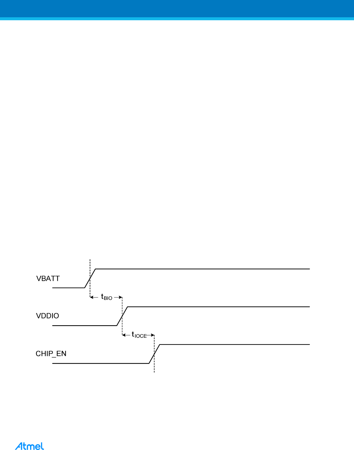
1.4 Power-Up Sequence
The power-up/down sequence for BTLC1000 is shown in Figure 1. The timing parameters are provided in Table
3.
Figure 1: Power-Up Sequence
Table 3: Power-Up Sequence Timing

BTLC1000-MR110CA [DATA SHEET]
Atmel-42376B-BTLC1000 Hardware Design Guide_02102015
4 4
Parameter Min Max Units Description Notes
t
BIO
0 ms VBATT rise to VDDIO rise VBATT and VDDIO can rise simultaneously or
can be tied together.
t
IOCE
0 ms VDDIO rise to CHIP_EN rise CHIP_EN must not rise before VDDIO. CHIP_EN
must be driven high or low, not left floating.
2 Application Information
The BTLC1000-MR110 module is fully self-contained. To use the module, just provide VBAT and VDDIO
supplies. See Table 2 for the recommended voltages.
3 Placement and Routing Guidelines
It is critical to follow the recommendations listed below to achieve the best RF performance:
• The board should have a solid ground plane. The center ground pad of the device must be solidly connected to
the ground plane by using a 3 x 3 grid of vias. Each ground pin of the module should have a ground via placed
either in the pad or right next to the pad going down to the ground plane.
• When the module is placed on the motherboard, a provision for the antenna must be made. There should be
nothing under the portion of the module which contains the antenna. This means the antenna should not be
placed directly on top of the motherboard PCB. This can be accomplished by, for example, placing the module
at the edge of the board such that the module edge with the antenna extends beyond the main board edge by
6.5mm. Alternatively, a cut out in the motherboard can be provided under the antenna. The cutout should be at
least 22mm x 6.5mm. Ground vias spaced 2.5mm apart should be placed all around the perimeter of the
cutout. No large components should be placed near the antenna.
• Keep away from antenna, as far as possible, large metal objects to avoid electromagnetic field blocking.
• Do not enclose the antenna within a metal shield.
• Keep any components which may radiate noise or signals within the 2.4GHz – 2.5GHz frequency band far
away from the antenna or better yet, shield those components. Any noise radiated from the main board in this
frequency band will degrade the sensitivity of the module.
3.1 Power and Ground
Dedicate one layer as a ground plane. Make sure that this ground plane does not get broken up by routes.
Power can route on all layers except the ground layer. Power supply routes should be heavy copper fill planes
to insure the lowest possible inductance. The power pins of the module should have a via directly to the power
plane as close to the pin as possible. Decoupling capacitors should have a via right next to the capacitor pin and
this via should go directly down to the power plane – that is to say, the capacitor should not route to the power
plane through a long trace. The ground side of the decoupling capacitor should have a via right next to the pad
which goes directly down to the ground plane. Each decoupling capacitor should have its own via directly to the
ground plane and directly to the power plane right next to the pad. The decoupling capacitors should be placed
as close to the pin that it is filtering as possible.

BTLC1000-MR110CA [DATA SHEET]
Atmel-42376B-BTLC1000 Hardware Design Guide_02102015
5
4 FCC Information
Each module has a label with an FCC ID, however the product User Manual must contain the following state-
ment: “This device complies with Part 15 of the FCC Rules. Operation is subject to the following two conditions:
(1) This device may not cause harmful interference, and (2) this device must accept any interference received,
including interference that may cause undesired operation”.
The module must be installed into the end product to provide a separation distance of at least 5 mm from all
persons and must not be co-located or operating in conjunction with any other antenna or transmitter.
If the module’s label is not visible when installed, then an additional permanent label referring to the enclosed
module: “Contains Transmitter Module FCC ID: 2ADHKBTLC1000” must be installed on the product in a visible
location.
This equipment has been tested and found to comply with the limits for a class B digital device, pursuant to part
15 of the FCC Rules. These limits are designed to provide reasonable protection against harmful interference in
a residential installation. This equipment generates, uses and can radiate radio frequency energy and if not
installed and used in accordance with the instructions, may cause harmful interference to radio communications.
However, there is no guarantee that interference will not occur in a particular installation. If this equipment does
cause harmful interference to radio or television reception, which can be determined by turning the equipment off
and on, the user is encouraged to try to correct the interference by one or more of the following measures:
- Reorient or relocate the module/product.
- Increase the separation between the equipment and module/product.
- Consult the dealer or an experienced radio/TV technician for help.
Changes and modifications made to the equipment without the approval of manufacturer could void the user's
authority to operate this equipment.
5 Interferers
One of the biggest problems with RF receivers is poor performance due to interferers on the board radiating
noise into the antenna or coupling into the RF traces going to input LNA. Care must be taken to make sure that
there is no noisy circuitry placed anywhere near the antenna or the RF traces. All noise generating circuits should
also be shielded so they do not radiate noise that is picked up by the antenna. Also, make sure that no traces
route underneath the RF portion of the BTLC1000. Also, make sure that no traces route underneath any of the
RF traces from the antenna to the BTLC1000 input. This applies to all layers. Even if there is a ground plane on
a layer between the RF route and another signal, the ground return current will flow on the ground plane and
Revision History
Atmel Corporation 1600 Technology Drive, San Jose, CA 95110 USA T: (+1)(408) 441.0311 F: (+1)(408) 436.4200 │ www.atmel.com
© 2014 Atmel Corporation.
Atmel Confidential: For Release Only Under Non-Disclosure Agreement (NDA)
Atmel®, Atmel logo and combinations thereof, Enabling Unlimited Possibilities®, and others are registered trademarks or trademarks of Atmel Corporation in U.S. and
other countries. ARM®, ARM Connected® logo, and others are the registered trademarks or trademarks of ARM Ltd. Other terms and product names may be trademarks
of others.
DISCLAIMER: The information in this document is provided in connection with Atmel products. No license, express or implied, by estoppel or otherwise, to any intellectual property right
is granted by this document or in connection with the sale of Atmel products. EXCEPT AS SET FORTH IN THE ATMEL TERMS AND CONDITIONS OF SALES LOCATED ON THE ATMEL
WEBSITE, ATMEL ASSUMES NO LIABILITY WHATSOEVER AND DISCLAIMS ANY EXPRESS, IMPLIED OR STATUTORY WARRANTY RELATING TO ITS PRODUCTS INCLUDING,
BUT NOT LIMITED TO, THE IMPLIED WARRANTY OF MERCHANTABILITY, FITNESS FOR A PARTICULAR PURPOSE, OR NON-INFRINGEMENT. IN NO EVENT SHALL ATMEL BE
LIABLE FOR ANY DIRECT, INDIRECT, CONSEQUENTIAL, PUNITIVE, SPECIAL OR INCIDENTAL DAMAGES (INCLUDING, WITHOUT LIMITATION, DAMAGES FOR LOSS AND
PROFITS, BUSINESS INTERRUPTION, OR LOSS OF INFORMATION) ARISING OUT OF THE USE OR INABILITY TO USE THIS DOCUMENT, EVEN IF ATMEL HAS BEEN ADVISED
OF THE POSSIBILITY OF SUCH DAMAGES. Atmel makes no representations or warranties with respect to the accuracy or completeness of the contents of this document and reserves
the right to make changes to specifications and products descriptions at any time without notice. Atmel does not make any commitment to update the information contained herein. Unless
specifically provided otherwise, Atmel products are not suitable for, and shall not be used in, automotive applications. Atmel products are not intended, authorized, or warranted for use
as components in applications intended to support or sustain life.
SAFETY-CRITICAL, MILITARY, AND AUTOMOTIVE APPLICATIONS DISCLAIMER: Atmel products are not designed for and will not be used in connection with any applications where
the failure of such products would reasonably be expected to result in significant p
ersonal injury or death (“Safety
-
Critical Applications”) without an Atmel officer's specific written consent.

BTLC1000-MR110CA [DATA SHEET]
Atmel-42376B-BTLC1000 Hardware Design Guide_02102015
6 6