Microchip Technology RN24 Bluetooth Module User Manual DSRN24 v2
Microchip Technology Inc. Bluetooth Module DSRN24 v2
Users Manual
RN-24 / RN25
www.rovingnetworks.com
DS-RN24-V2 1/28/2009
809 University Avenue • Los Gatos, CA 95032 • Tel (408) 395-6539 • info@RovingNetworks.com
Class 1 Bluetooth® Super
Module
Features
• Supports Bluetooth 2.1/2.0/1.2/1.1 and
v2.0+EDR
• Embedded SPP/DUN stack support, no
host or processor stacks required
• Small-form factor 24 Pin DIP package (0.1”
pitch X 0.9” socket width)
• Accepts 4Vdc to 24Vdc power
• Serial port signals on TTL, RS- 232 and
RS-485 levels.
• RS-485 signaling with auto-direction control
(PCB rev 4 )
• UART baud rate speeds: 1200bps up to
921.6Kbps
• 9 General Purpose Input/Output Pins (4ma
source/sink) controlled via remote
commands
• 2 Channel 8 Bit AD converter (5Hz, 0-
1.8VDC )
• LEDs indicate connection and RX/TX status
• On board antenna or external SMA jack
• Low power consumption (30mA
connected,, <10mA sniff mode)
• Programmable over local UART and
remotely from any Bluetooth client
o Simple ACSII command interface
• UART (SPP or HCI) and USB (HCI only) data
connection interfaces
• Sustained SPP data rates - 240Kbps (slave),
300Kbps (master)
• Embedded Bluetooth stack profiles included
(requires no host stack): GAP, SDP,
RFCOMM and L2CAP protocols, with SPP
and DUN profile support.
Applications
• Wireless RS232/RS485 cable replacement
• Remote equipment monitoring
• Scanners, GPS and measurement systems
• Industrial sensors and controls
• Medical devices
Description
The RN24 transforms your product’s serial interface
into a wireless connection. The RN24 is a Class 1
Bluetooth radio with auto-connect and connect on RX
data features, enabling your product to transfer data
up to 100M. The RN24 accepts a wide range of
unregulated DC power. The DIP packaging with
GPIO, UART interfaces and AD converter makes it
the perfect prototyping module and allows products to
have optional Bluetooth capability when the module
is plugged in.
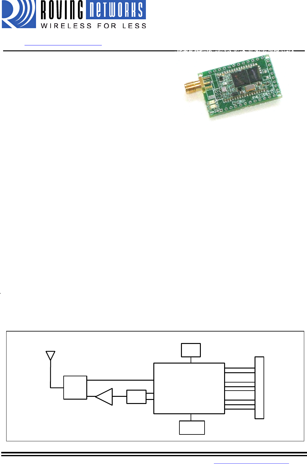
Block Diagram
CSR BlueCore-04
External
BALUN
PA
RF
Switch
Crystal
Flash
Memory
GND
VCC
USB
UART
PCM
PIO6
PIO5
PIO4
DS-RN24_V2 1/28/2009
809 University Avenue • Los Gatos, CA 95032 • Tel (408) 395-6539 • info@RovingNetworks.com
Overview
UART baud rate speeds: 1200bps up to 921Kbps, non-standard baud rates can be programmed.
Class 1 radio, 330’ (100m) distance, 12dBm output transmitter, -80dBm typical receive sensitivity
Frequency 2402 ~ 2480MHz,
FHSS/GFSK modulation, 79 channels at 1MHz intervals
Secure communications, 128 bit encryption
Error correction for guaranteed packet delivery
UART local and over-the-air RF configuration
Auto-discovery/pairing requires no software configuration (instant cable replacement).
Auto-connect master, IO pin (DTR) and character based trigger modes
Environmental Conditions
Parameter Value
Temperature Range (Operating)
-40
o
C ~ 85
o
C
Temperature Range (Storage) -40
o
C ~ 85
o
C
Relative Humidity (Operating) ≤90%
Relative Humidity (Storage) ≤90%
Electrical Characteristics
Power supply voltage
WARNING – Only one source
of power must be supplied.
3.3Vdc + 0.1V and 10mVp-p max. noise
OR
4-24VDC unregulated .
Parameter Min Typ. Max. Unit
Supply Voltage (DC) 3.0 3.3 3.6 V
RX Supply Current 35 60 mA
TX Supply Current 65 100 mA
Average power consumption
Standby/Idle (default settings) 25 mA
Connected (normal mode) 30 50 mA
Connected (low power Sniff) 8 mA
Standby/Idle (lowest power) 250uA 2.5 mA
DS-RN24_V2 1/28/2009
809 University Avenue • Los Gatos, CA 95032 • Tel (408) 395-6539 • info@RovingNetworks.com
Digital I/O Characteristics
WARNING: Take care not to exceed the voltage limits to the VCC, TTL SERIAL, and GPIO pins. 0 negative
voltage or voltage exceeding 3.30 VDC can permanently damage the device!
• Use a 10KΩ series resistor on inputs
• GPIO sink current is 4mA max.
• Unused pins should float
2.7V ≤ VDD ≤ 3.0V Min Typ. Max. Unit
Input logic level LOW -0.4 - +0.8 V
Input logic level HIGH 0.7VDD - VDD+0.4 V
Output logc level LOW - - 0.2 V
Output logic level HIGH VDD-0.2 - - V
All I/O’s (except reset) default to weakpull down
+0.2 +1.0 +5.0 uA
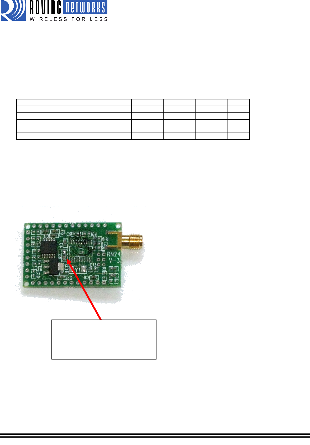
The RN24 can drive either UART signals on the TTL pins 8-11 or RS232 pins 13-16. WARNING: Driving the TTL
signals at RS232 levels can permanently damage the module. By default the module is configured to drive only
the RS232 pins. To drive the TTL signals you must remove the resistor R7. R7 can be found on the bottom of
the board, near the center.
Remove R7 to enable the UART
TTL signaling on pins 8-11.
This will disconnect pins 13-16
from the UART interface.
DS-RN24_V2 1/28/2009
809 University Avenue • Los Gatos, CA 95032 • Tel (408) 395-6539 • info@RovingNetworks.com
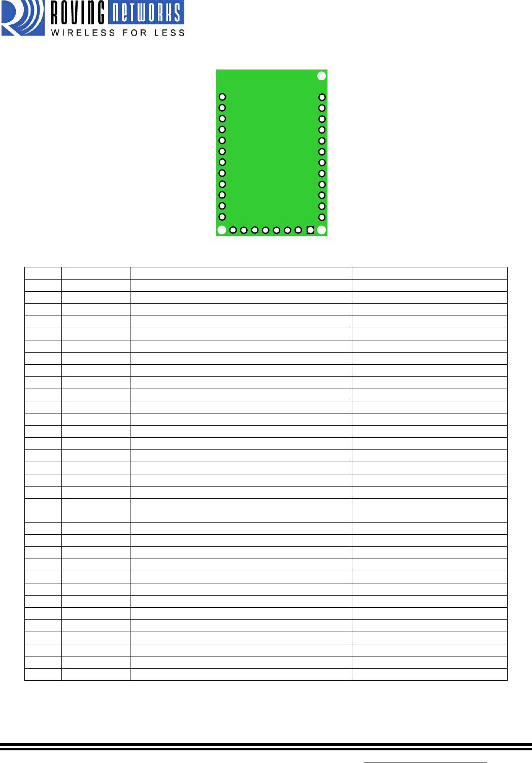
Pin Description
NOTE:
The Power can be applied to
either pin 12, or pin 3, but NOT both.
If pin 12 is powered then Pin 3 can be
used as a 3.3V regulated supply
output up to 200mA.
Pin Name Description Default
1 RESET Active HIGH Has 1K pulldown
2 GND
3 VCC 3.3V power (Only for RN24) Mutually exclusive with Pin 12
4 SPI_CS Programming Only No Connect
5 SPI_CK Programming Only
No Connect
6 SPI_MO Programming Only
No Connect
7 SPI_MI Programming Only
No Connect
8 CTS Input, if set HIGH disables transmitter TTL input
9 TX Transmit output TTL output
10 RTS Output, goes HIGH to disable host transmitter TTL output
11 RX Receive input TTL input
12 VDD 4-24V unregulated DC power (RN24 or RN25) Mutually exclusive with Pin 3
13 UART_TX Receive input RS-232 level signaling
14 UART_RX Transmit output RS-232 level signaling
15 UART_RTS Output, goes HIGH to disable host transmitter RS-232 level signaling
16 UART_CTS Input, if set HIGH disables transmitter RS-232 level signaling
17 GPIO-7 Default baud rate, HIGH = 9600, LOW = 115K Input to RN24, default = LOW
18 GPIO-6 Enable auto master mode = HIGH Input to RN24, default = LOW
19 GPIO-4 Restore factory defaults Set HIGH then toggle for 5
msec. 3 times
20 GPIO-3 Enable instant cable mode = HIGH Input to module, default = LOW
21 GPIO-2 Connection status, connected=HIGH Output from module
22 RS-485 D+ RS485 signaling (Only on RN25) (Auto direction detect)
23 RS-485 D- RS485 signaling (Only on RN25) (Auto direction detect)
24 GND Ground
25 GPIO-11
26 GPIO-8 Controls red LED
27 GPIO-9 Controls yellow LED
28 GPIO-10
29 NC
30 NC
31 NC
32 GND Ground
RN24/RN25
1
2
3
4
5
6
7
8
9
10
11
12
Top view
24
23
22
21
20
19
18
17
16
15
14
13
32 31 3 0 29 28 27 26 25
RN24/RN25
1
2
3
4
5
6
7
8
9
10
11
12
Top view
24
23
22
21
20
19
18
17
16
15
14
13
32 31 3 0 29 28 27 26 25
DS-RN24_V2 1/28/2009
809 University Avenue • Los Gatos, CA 95032 • Tel (408) 395-6539 • info@RovingNetworks.com
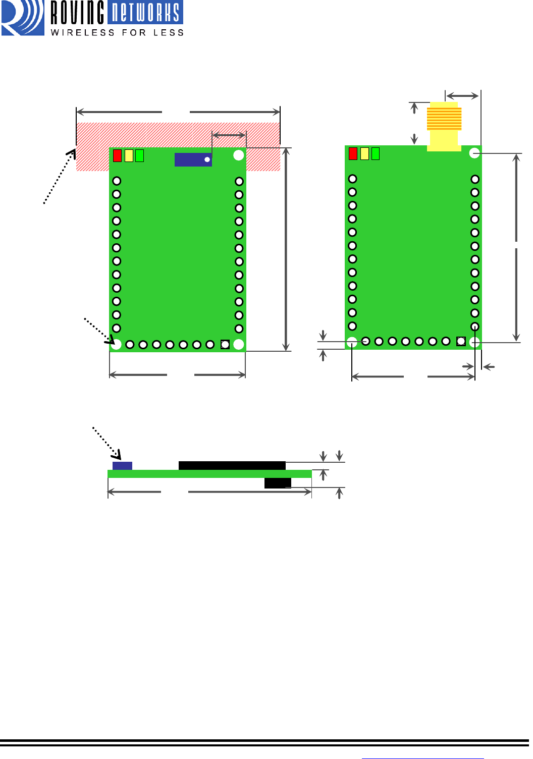
Module Dimensions
Connect with 24 pin DIP (through-hole) 0.1” pitch and 0.9” wide socket
Single row mating sockets use:
Digikey P/N: ED7012-ND (female)
ED7512-ND (male)
1500 mil
65 mil
Antenna
200 mil
1500 mil
65 mil
Antenna
200 mil
1
2
3
4
5
6
7
8
9
10
11
12
RN24/RN25
RN24-E/RN25-E
Top view
24
23
22
21
20
19
18
17
16
15
14
13
32 31 30 29 28 2 7 26 25
1400 mil
320 mil
100 mi
LED
LED
LED
230 mil
900 mil
110 mil
1
2
3
4
5
6
7
8
9
10
11
12
RN24/RN25
RN24-E/RN25-E
Top view
24
23
22
21
20
19
18
17
16
15
14
13
32 31 30 29 28 2 7 26 25
1400 mil
320 mil
100 mi
LED
LED
LED
230 mil
900 mil
110 mil
1500 mil
245 mil
RN24/RN25
RN24-S/RN25-S
Top view
24
23
22
21
20
19
18
17
16
15
14
13
32 31 30 29 28 2 7 26 25
1000 mil
LED
LED
LED
80 mil diameter
Mounting hole
Keep metallic components,
connec tors, copper traces,
and ground planes away from
antenna area
1600 mil
1
2
3
4
5
6
7
8
9
10
11
12
245 mil
RN24/RN25
RN24-S/RN25-S
Top view
24
23
22
21
20
19
18
17
16
15
14
13
32 31 30 29 28 2 7 26 25
1000 mil
LED
LED
LED
80 mil diameter
Mounting hole
Keep metallic components,
connec tors, copper traces,
and ground planes away from
antenna area
1600 mil
1
2
3
4
5
6
7
8
9
10
11
12
DS-RN24_V2 1/28/2009
809 University Avenue • Los Gatos, CA 95032 • Tel (408) 395-6539 • info@RovingNetworks.com
Design Concerns
1. Reset circuit. RN-24 contains a 1k pulldown, the polarity of reset is ACTIVE HIGH.
A power on reset circuit with delay is OPTIONAL on the reset pin of the module. It should only be required if the
input power supply has a very slow ramp, or tends to bounce or have instability on power up. Often a
microcontroller or embedded CPU IO is available to generate reset once power is stable
2. Factory reset PIO4. It is a good idea to connect this pin to a switch, or jumper, or resistor, so it can be
accessed. This pin can be used to reset the module to FACTORY DEFAULTS and is often critical in situations
where the module has been mis-configured.
3. Connection status. PIO5 is available to drive an LED, and blinks at various speeds to indicate status. PIO2 is
an output which directly reflects the connection state, it goes HIGH when connected, and LOW otherwise.
4. RS485 support. RS-485 signaling with auto-direction control is ONLY supported on PCB rev 4 and later. Treat
pins 22 and 23 as no connect on previous PCB boards.
5. Using SPI bus for flash upgrade. While not required, this bus is very useful for configuring advanced
parameters of the Bluetooth modules, and is required for upgrading the firmware on modules. The suggested ref-
design shows a 6pin header which can be implemented to gain access to this bus. A minimum-mode version
could just use the SPI signals (4pins) and pickup ground and VCC from elsewhere on the design.
6. Minimizing Radio interference. When integrating the RN24 DIP module with on board chip antenna be sure
the area around the chip antenna end of RN24-S module protrudes at least 5mm from the PCB and any metal
enclosure. If this is not possible use the RN24-E.
7. Soldering Reflow Profile.
• Lead-Free Solder Reflow
• Temp: 230 degree C , 30-40 seconds, Peak 250 degree C maximum.
• Preheat temp: 165 +- 15 degree C, 90 to 120 seconds.
• Time: Single Pass, One Time
8. Connecting to the GPIO. Placing 3.3Vdc into the PIO’s while they are set as outputs will permanently damage
the radio. The failure mode is short across GND and VCC. Use a 10KO resistor is series or a 10KO pull up
resistor for input and output PIO’s respectively.
• Make sure to connect a common ground when using the external TX, RX inputs on the 0 – 3.3Vdc
• For a 3 wire DB-9 interface (tx, rx, gnd only) connect/short CTS to RTS, Factory default is hardware flow
control enabled CTS and RTS connected.
• When using a 5.0Vdc Input, PIO’s require a 10K ohm series resistor. PIO’s are 0-3.3Vdc not 5 volt tolerant.
Compliance Information
• FCC Certified, FCC ID T9J-RN24, IC number6514A-RN24
• Environmentally friendly RoHS compliant
Ordering Information
Part Number Description
RN-24-S With chip antenna
RN-24-E With SMA jack
RN-25-S RS485 signaling with chip antenna
RN-25-E RS485 signaling with SMA jack
DS-RN24_V2 1/28/2009
809 University Avenue • Los Gatos, CA 95032 • Tel (408) 395-6539 • info@RovingNetworks.com
RN-SMA-S 1” external antenna “Stuby”
RN-SMA-4 4” high performance antenna
For other configurations, contact Roving Networks directly.
Visit http://www.rovingnetworks.com for current pricing and a list of distributors carrying our products.
Copyright © 2009 Roving Networks. All rights reserved.
The Bluetooth trademark and logo are registered trademarks and are owned by the Bluetooth SIG, Inc. All other
trademarks are property of their respective owners.
Roving Networks reserves the right to make corrections, modifications, and other changes to its products,
documentation and services at any time. Customers should obtain the latest relevant information before placing
orders and should verify that such information is current and complete.
Roving Networks assumes no liability for applications assistance or customer product design. Customers are
responsible for their products and applications using Roving Networks components. To minimize the risks associated
with customer products and applications, customers should provide adequate design and operating safeguards.
Roving Networks products are not authorized for use in safety-critical applications (such as life support) where a
failure of the Roving Networks product would reasonably be expected to cause severe personal injury or death,
unless officers of the parties have executed an agreement specifically governing such use.

Federal Communications Commission (FCC) Requirements
This equipment has been tested and found to comply with the limits for a Class B digi
tal device, pursuant to part 15 of the FCC rules. These limits are designed to provide r
easonable protection against harmful interference in a residential installation.
This equipment generates uses and can radiate radio frequency energy and, if not insta
lled and used in accordance with the instructions, may cause harmful interference to r
adio communications. However, there is no guarantee that interference will not occur
in a particular installation. If this equipment does cause harmful interference to radio
or television reception, which can be determined by turning the equipment off and on,
the user is encouraged to try to correct the interference by one or more of the followi
ng measures:
Reorient or relocate the receiving antenna.
Increase the separation between the equipment and receiver.
Connect the equipment into an outlet on a circuit different from that to which the
receiver is connected.
Consult the dealer or an experienced radio/TV technician for help.
FCC Caution :
To assure continued compliance, any changes or modifications not expressly
approved by the party responsible for compliance could void the user's authority to
operate this equipment. (Example - use only shielded interface cables when
connecting to computer or peripheral devices).
This Transmitter must not be colocated or operating in conjunction with any other ant
enna or transmitter. Any changes or modifications (including the antennas) made to th
is device that are not expressly approved by the manufacturer may void the user’s aut
hority to operate the equipment.
End Product Labeling
This transmitter module is authorized only for use in devices where the antenna may b
e installed such that 20 cm may be maintained between the antenna and users. The fin
al end product must be labeled in visible area with the following:
“Contains FCC ID: T9J-RN24 ”
End Product Manual Information
The user manual for end users must include the following information in a prominent
location “IMPORTANT NOTE: To comply with FCC RF exposure compliance requir
ements, the antenna used for this transmitter must be installed to provide a separation
distance of at least 20cm from all persons and must not be colocated or operating in c
onjunction with any other antenna or transmitter.”
This device complies with part 15 of the FCC rules. Operation is subject to the followi
ng two conditions
(1) This device may not cause harmful interference and
(2) This device must accept any interference received, including interference that may
cause undesired operation.
IMPORTANT NOTE:
In the event that these conditions can not be met (for example certain laptop configura
tions or colocation with another transmitter), then the FCC authorization is no longer
considered valid and the FCC ID can not be used on the final product. In these circum
stances, the OEM integrator will be responsible for reevaluating the end product (incl
uding the transmitter) and obtaining a separate FCC authorization.
This device is intended only for OEM integrators under the following conditions: The
antenna must be installed such that 20 cm is maintained between the antenna and user
s. As long as a condition above is met, further transmitter test will not be required. Ho
wever, the OEM integrator is still responsible for testing their end product for any
additional compliance requirements required with this module installed (for example
, digital device emissions, PC peripheral requirements, etc.).