Microelectronics Technology RU00-M06 RFID PCA MODULE PCIE M.2 UHF US/JP BAND User Manual rev2
Microelectronics Technology Inc RFID PCA MODULE PCIE M.2 UHF US/JP BAND Users Manual rev2
Users Manual_rev2.pdf
RFID MODULE PCIE M.2 Quick Guide
Version 1.0.0
MTI
Group
Proprietary Information
Any unauthorized use, duplication, reproduction, reverse engineering,
decompilation, or disclosure of this document may be considered as
infringement of MTI Group’s intellectual property rights, the infringer may
be accused and liable applicable legal penalties.
Copyright, Microelectronics Technology Inc.. All rights reserved.

MICROELECTRONICS TECHNOLOGY INC 2 September 15, 2017
Table of Contents
1 Introduction ................................................................................................................................................. 3
2 Regulatory Statement ................................................................................................................................. 4
3 System Block Diagram ................................................................................................................................. 6
4 Specifications ............................................................................................................................................... 7
5 Pin Configurations and Descriptions ........................................................................................................... 8
6 Package Information ................................................................................................................................. 10
Package Mechanical Outline ..................................................................................................... 10
7 Interfacing to the PCIe M.2 Module .......................................................................................................... 11
8 Operating the PCIe M.2 Module ............................................................................................................... 12
9 Revision History ......................................................................................................................................... 13
Figures
Figure 1: System Block Diagram ......................................................................................................................... 6
Figure 2: Pin Configurations ............................................................................................................................... 8
Figure 3: Package Mechanical Outline.............................................................................................................. 10
Tables
Table 1: Band configurations .............................................................................................................................. 3
Table 2: Specifications ........................................................................................................................................ 7
Table 3: Pin Configurations ................................................................................................................................. 9
Table 4: Revision history ................................................................................................................................... 13
MICROELECTRONICS TECHNOLOGY INC 3 September 15, 2017
1 Introduction
The PCIe M.2 Module that comprises a completely in integrated solution for EPC Gen 2 / ISO18000-63
(formerly 18000-6C) application.
The PCIe M.2 Module was developed to make embedding UHF RFID reader capability easy. The PCIe M.2
Module builds on market-leading Indy reader chip technology and integrates all of the necessary
components into a tiny package. It requires very few external components.
Model Number Supported Regions Operating Frequency
RU00-M06-X002
US 902.75MHz~927.25MHz
JP 916.8MHz~920.4MHz
920.6MHz, 920.8MHz
Table 1: Band configurations

MICROELECTRONICS TECHNOLOGY INC 4 September 15, 2017
2 Regulatory Statement
Federal Communication Commission Interference Statement
This device complies with Part 15 of the FCC Rules. Operation is subject to the following two conditions: (1)
This device may not cause harmful interference, and (2) this device must accept any interference received,
including interference that may cause undesired operation.
This equipment has been tested and found to comply with the limits for a Class B digital device, pursuant to
Part 15 of the FCC Rules. These limits are designed to provide reasonable protection against harmful
interference in a residential installation. This equipment generates, uses and can radiate radio frequency energy
and, if not installed and used in accordance with the instructions, may cause harmful interference to radio
communications. However, there is no guarantee that interference will not occur in a particular installation. If
this equipment does cause harmful interference to radio or television reception, which can be determined by
turning the equipment off and on, the user is encouraged to try to correct the interference by one of the
following measures:
- Reorient or relocate the receiving antenna.
- Increase the separation between the equipment and receiver.
- Connect the equipment into an outlet on a circuit different from that
to which the receiver is connected.
- Consult the dealer or an experienced radio/TV technician for help.
FCC Caution: Any changes or modifications not expressly approved by the party responsible for compliance
could void the user's authority to operate this equipment.
Radiation Exposure Statement:
This equipment complies with FCC radiation exposure limits set forth for an uncontrolled environment. This
equipment should be installed and operated with minimum distance 20cm between the radiator & your body.
MICROELECTRONICS TECHNOLOGY INC 5 September 15, 2017
This transmitter must not be co-located or operating in conjunction with any other antenna or transmitter.
This device is intended only for OEM integrators under the following conditions:
1) The antenna must be installed such that 20 cm is maintained between the antenna and users, and
2) The transmitter module may not be co-located with any other transmitter or antenna.
As long as 2 conditions above are met, further transmitter test will not be required. However, the OEM
integrator is still responsible for testing their end-product for any additional compliance requirements
required with this module installed.
IMPORTANT NOTE: In the event that these conditions cannot be met (for example certain laptop
configurations or co-location with another transmitter), then the FCC authorization is no longer considered
valid and the FCC ID cannot be used on the final product. In these circumstances, the OEM integrator will be
responsible for re-evaluating the end product (including the transmitter) and obtaining a separate FCC
authorization.
End Product Labeling
FOR MOBILE DEVICE USAGE (>20cm/low power)
This transmitter module is authorized only for use in device where the antenna may be installed such that 20
cm may be maintained between the antenna and users. The final end product must be labeled in a visible
area with the following: “Contains FCC ID:MAD-RU00-M06”. The grantee's FCC ID can be used only when all
FCC compliance requirements are met.
Manual Information To the End User
The OEM integrator has to be aware not to provide information to the end user regarding how to
install or remove this RF module in the user’s manual of the end product which integrates this
module.
The end user manual shall include all required regulatory information/warning as show in this manual.
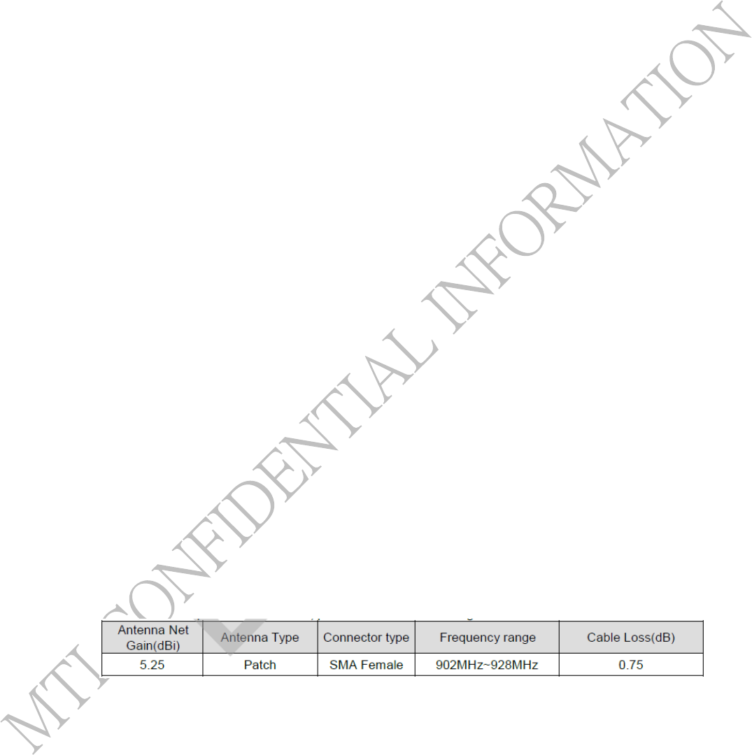
Antenna information:
::
:
*The connector transformer is needed
MICROELECTRONICS TECHNOLOGY INC 6 September 15, 2017
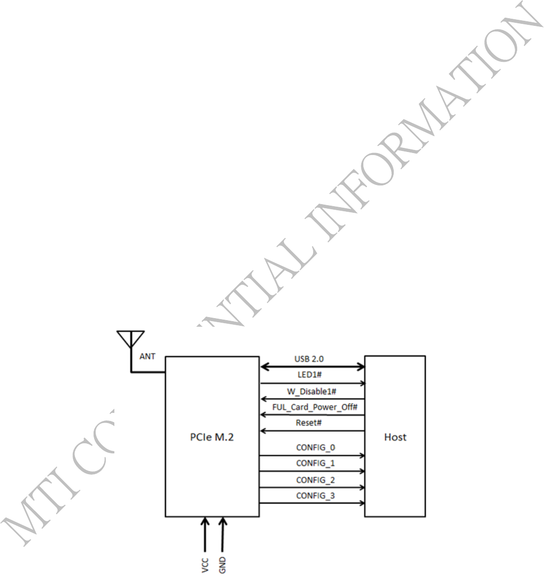
3 System Block Diagram
An example of a PCIe M.2 Module system-level block diagram for an embedded application is shown in
Figure 1.
Required connections:
VCC and GND are required to power the PCIe M.2 Module.
RF pin must be connected to the OEM antenna.
USB 2.0 provides host communications to control the operation of the PCIe M.2 Module.
Recommended connections:
LED1#: This signal is used to allow the add-in card to provide status indicators via LED devices that will
be provided by the system.
W_DISABLE1# : This signal allow users to disable, via a system-provided switch, the add-in card’s radio
operation in order to meet public safety regulations or when otherwise desired.
FULL_CARD_POWER_OFF# : This signal is an Active Low input that is used to turn off the entire module.
RESET#: This pin is active, the modem will immediately be placed in a Power On reset condition.
Optional connections:
CONFIG0-4: These signals provide the means to indicate the specific configuration of the module as
well as indication of whether a module is present or not.
(The PCIe M.2 Module default setting: CONFIG_0, 3 N/A, CONFIG_1, 2 Ground.)
Figure 1: System Block Diagram

MICROELECTRONICS TECHNOLOGY INC 7 September 15, 2017
4 Specifications
Item Description Specifications
1 RFID Protocol & Profiles EPCglobal UHF Class 1 Gen 2 / ISO18000-6C
2 Transmit Power +10dBm to +27dBm
3 Transmit Power Accuracy
Room Temp.
• +/- 1.0dB @ +24dBm~ +27dBm
• +/- 1.5dB @ +10dBm ~+24dBm
Low/High Temp.
• +/- 1.5dB @ +24dBm ~+27dBm
• +/- 2.0dB @ +10dBm ~+24dBm
4 Transmit Mask DRM Compliance Compliance at +25 dBm
5
Support Regions
•US:902MHz~928MHz
•JP:916.8MHz~920.8MHz
6 RF Antenna Port MHF4(M)*1, mono-static
7 Return Loss at ports 12 dB
8 Receive Sensitivity at port -74dBm @DRM profile, 15 dB antenna return loss, 27dBm
output power.
9 Interference Rejection at port +10dBm
10 DC Power Supply 3.135 V~4.4V
11 DC Power Typ. 4.5 W at + 27 dBm
12 Power modes
Ready: MCU Ready only
Standby : MCU and XCVR Ready
W_Disable: Go to Ready mode
Full_Card_Power_Off : Full Power Off
13 Digital Connector PCIe M.2 form factor
14 Host Control Signal USB 2.0 compliant with full speed operation
15 Software API MTI Low Level Command set
Table 2: Specifications
MICROELECTRONICS TECHNOLOGY INC 8 September 15, 2017
5 Pin Configurations and Descriptions
The module is 75-pin PCIe M.2 Key B. The pin configurations are shown in Figure
4 3.3V
2 3.3V
72
74
10 LED1#( O/3.3V)
8 W_DISABLE#( I/3.3V)
6 FULL_CARD_POWER_OFF#( I/1.8V)
16 Module Key
14 Module Key
12 Module Key
22 N/C
20 N/C
18 Module Key
28 N/C
26 N/C
24 N/C
34 N/C
32 N/C
30 N/C
40 N/C
38 N/C
36 N/C
46 N/C
44 N/C
42 N/C
52 N/C
50 N/C
48 N/C
58 N/C
56 N/C
54 N/C
62 N/C
60 N/C
70 3.3V
68 N/C
66 N/C
GND 5
GND 3
CONFIG_3 1
GND 11
USB_D- 9
USB_D+ 7
Module Key 17
Module Key 15
Module Key 13
N/C 23
CONFIG_0 21
Module Key 19
N/C 29
GND 27
N/C 25
N/C 35
GND 33
N/C 31
N/C 41
GND 39
N/C 37
N/C 47
GND 45
N/C 43
N/C 53
GND 51
N/C 49
N/C 59
GND 57
N/C 55
N/C 63
N/C 61
GND 71
CONFIG_1 69
RESET#( I/1.8V) 67
CONFIG_2
3.3V
75
GND 73
3.3V
N/C 65
64 N/C
Figure 2: Pin Configurations
MICROELECTRONICS TECHNOLOGY INC 9 September 15, 2017
Pin
Number
Pin Name Type Description
1 CONFIG_3 Output
N/A (*1)
2 3.3V Power Power Supply
3
GND
Ground
Ground
4
3.3V
Power
Power Supply
5 GND Ground Ground
6FULL_CARD_PO
WER_OFF#
Input General Purpose Input/Output (*2)
7 USB_D+ I/O USB Data ± Differential defined in the USB 2.0
Specification
8 W_DISABLE1# Input General Purpose Input/Output
9 USB_D- I/O USB Data ± Differential defined in the USB 2.0
Specification
10 LED1# Output General Purpose Input/Output
11 GND Ground
Ground
12,13,14,15,16.17
,18,19
Module Key N/A
20 N/C N/A
21 CONFIG_0 Output Ground (*1)
22,23,24,25,26 N/C N/A
27 GND Ground
Ground
28,29,30,31,32 N/C
N/A
33 GND Ground
G
34,35,36,37,38 N/C
N/A
39 GND Ground Ground
40,41,42,43,44
N/C
N/A
45
GND
Ground
G
46,47,48,49,50
N/C
N/A
51
GND
Ground
Ground
52,53,54,55,56 N/C N/A
57 GND Ground Ground
58,59,60,61,62,63
,64,65,66
N/C N/A
67
RESET#
Input
General Purpose Input/Output (*2)
68
N/C
N/A
69
CONFIG_1
Output
Ground (*1)
70
3.3V
Power
Power Supply
71
GND
Ground
Ground
72
3.3V
Power
Power Supply
73
GND
Ground
Ground
74
3.3V
Power
Power Supply
75
CONFIG_2
Output
N/A (*1)
Table 3: Pin Configurations
(*1) CONFIG_0, 3 connector to N/A, CONFIG_1, 2 connector to Ground Main Host interface for WWAN-
PCIe
(*2) General Purpose Input / Output voltage is 1.8V
MICROELECTRONICS TECHNOLOGY INC 10 September 15, 2017
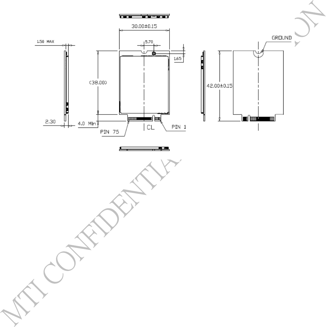
6 Package Information
Package Mechanical Outline
Figure 3: Package Mechanical Outline
MICROELECTRONICS TECHNOLOGY INC 11 September 15, 2017
7 Interfacing to the PCIe M.2 Module
Power and Ground
All circuits on the PCIe M.2 Module are powered from inputs at pin 2, 4, 70, 72 and 74. The PCIe M.2
Module operates with any supply voltage between 3.135 and 4.4V, The Power pins follow PCIe M.2
design rule.
Communication
The PCIe M.2 Module has one USB 2.0 ports. The USB are compatible with a standard USB 2.0. The user’s
host processor issues IRI commands to the HOST USB, which can be configured for any standard USB 2.0.
RF
The PCIe M.2 Module is configured for monostatic operation, which requires only a single RF port for full
duplex communication. The output must be routed to the antenna via 50 ohm. To maximize the radiated
power (and corresponding communication range), the length of the transmission line between PCIe M.2
Module and antenna should be made as short as possible.
W_Disable1#
W_Disable1# is wireless disable signals that are provided for wireless communications add-in cards. This
signal allow users to disable, via a system-provided switch, the add-in card’s radio operation in order to
meet public safety regulations or when otherwise desired. Implementation of wireless disable signals is
applicable to systems and all add-in cards that implement radio frequency capabilities.
Full_Card_Power_Off#
FULL_CARD_POWER_OFF# signal is an Active Low input that is used to turn off the entire module. When the
input signal is asserted high ( 1.19 V) the Module will be enabled. When the input signal is driven low signal
(≤0.2 V) or Tri-stated, it will force the module to shut down.
Reset#
Asynchronous RESET# pin, active low. Whenever this pin is active, the modem will immediately be placed in a
Power On reset condition. Care should be taken not to activate this pin unless there is a critical failure and all
other methods of regaining control and/or communication with the PCIe M.2 Module have failed.
When the input signal is asserted high ( 1.19 V) the Module will be operation mode. When the input signal is
driven low signal (≤0.2 V) the Module will be reset PCIe M.2 Module.
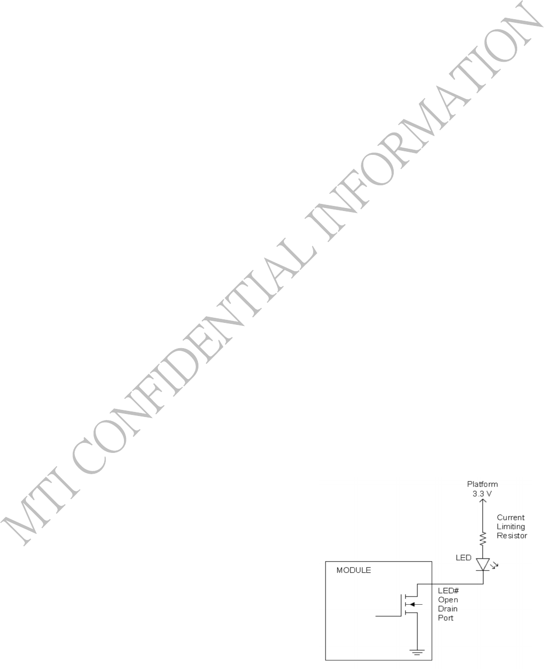
LED_1#
Open drain, active low signal. This signals is used to allow the
add-in card to provide status indicators via LED devices that
will be provided by the system.

MICROELECTRONICS TECHNOLOGY INC 12 September 15, 2017
8 Operating the PCIe M.2 Module
Once the required hardware connections are made to the PCIe M.2 Module, the unit can be operated with
simple software routines running on the OEM’s host processor. The host software issues commands to
configure the reader, set the reader’s idle mode and to start and stop various Gen2 RFID reader operations.
An example of the sequence of events starting at reader power-up is:
1. Apply 3.135V~4.4V power to the PCIe M.2 Module.
2. Establish a connection to the device via the host software.
3. Configure the reader. Critical parameters are:
a. Region of operation
When configured for a specific region, the PCIe M.2 Module can operate only according to the air
interface standards for that region. Key communication parameters are not adjustable by the user but
are inherent in the PCIe M.2 Module firmware. The FCC regional operation is the default for the device.
NOTE: The OEM is strictly forbidden to operate the PCIe M.2 Module in a regional mode other than
that in which the device is located. Applicable agency certification must be obtained by the OEM for
their product to operate in the region in which it is located. The modular certification of the PCIe M.2
Module in the U.S. may only be utilized by OEM’s that follow all guidelines set forth in this document.
b. RF output power
The PCIe M.2 Module output power must be set to a level between 10 and 27dBm. The default power
is set to the reader’s maximum allowable of 27dBm.
4. Initiate an RFID operation.
Gen2 RFID operations including Inventory, Read, Write, Lock and Kill are initiated with a command.
5. Set the PCIe M.2 Module standby mode.
When the PCIe M.2 Module is not executing an RFID operation, it assumes a low power state until another
RFID function is initiated by the host.
MICROELECTRONICS TECHNOLOGY INC 13 September 15, 2017
9 Revision History
Version
Number Description Revision Date
1.0.0 Initial release 15-Sep-17
Table 4: Revision history