MARKING & DECODING 2D SYMBOLOGIES
2012-08-20
: Microscan Marking Decoding 2D Symbologies Marking_Decoding_2D_Symbologies Webinars
Open the PDF directly: View PDF ![]() .
.
Page Count: 22
- MARKING & DECODING 2D SYMBOLOGIES
- About Your Instructors
- Today’s Objectives
- Today’s Topics
- Marking Methods
- Selecting a Symbology
- Marking Methods
- Marking Methods
- Marking Methods
- Marking Methods
- Marking Methods
- Decoding 2D Symbols
- Capture an Image
- Decoding a 2D Symbol
- Decoding a 2D Symbol
- Maximizing Readability
- Decodability
- Decodability
- Decodability
- Marking & Decoding 2D Symbologies
- Next session….
- Thank you!

Track, Trace & Control Solutions
© 2010 Microscan Systems, Inc.
MARKING & DECODING 2D
SYMBOLOGIES

© 2010 Microscan Systems, Inc.
About Your Instructors
Matt Van Bogart
Global Channel Manager
Joined Microscan in 1999
Held management positions in
Marketing, Product Management
and Sales
Juan Worle
Technical Training Coordinator
With Microscan since 1996
Held positions in Service, Applications,
Sales and Marketing

© 2010 Microscan Systems, Inc.
Today’s Objectives
By the end of today’s Webinar, you will know
Proper marking techniques for your application &
maximizing readability
Different marking methods available
How a 2D symbol is decoded

© 2010 Microscan Systems, Inc.
Today’s Topics
Selecting a Symbology
Marking Methods
Decoding a 2D Symbol
Maximizing Readability
Decodability
© 2010 Microscan Systems, Inc.
MARKING METHODS

© 2010 Microscan Systems, Inc.
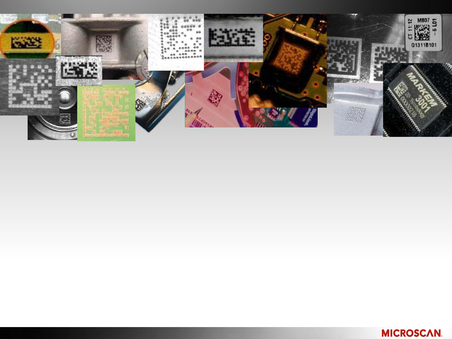
Selecting a Symbology
Select a Symbology
Many things to consider:
–Space, surface shape & quality
–Amount of data
–Cost of equipment (printer type, scanner vs. imager, consumables)
–Cosmetic, product appearance
–Type of equipment down the supply chain
Some applications may only require a laser scanner
–Good contrast, non-reflective material, flat surface
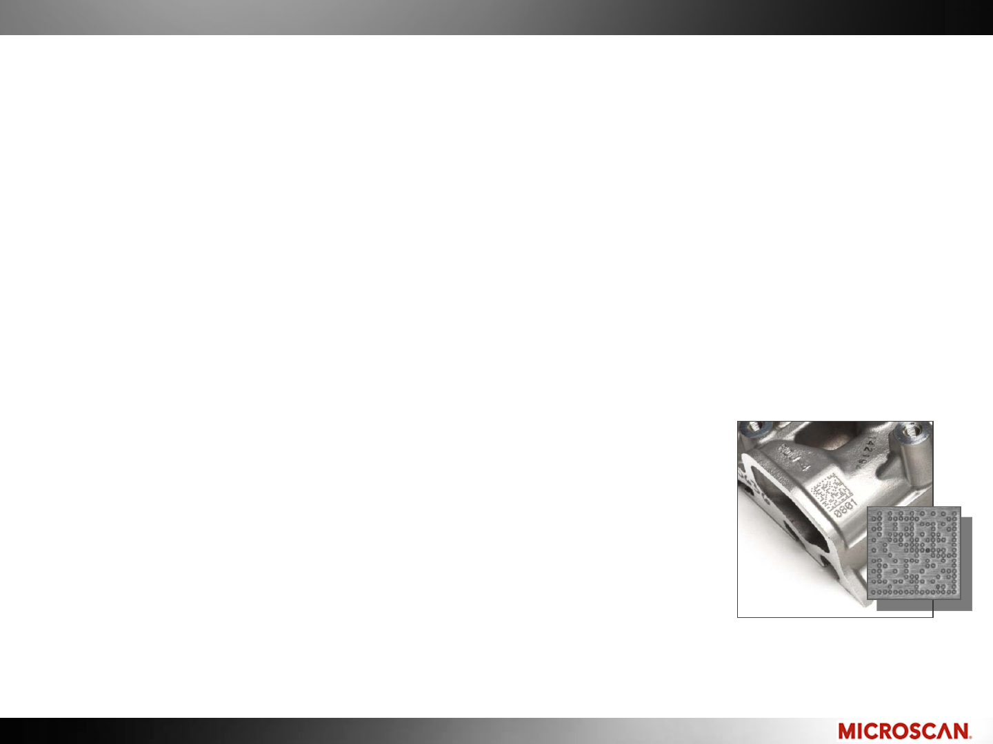
Data Matrix is more common for DPM
–Easy to make with many marking methods
–Easy to decode on different substrates
–Error correction recovers from misprints
and damage
Some DPM marks can be
decoded with a laser scanner
© 2010 Microscan Systems, Inc.
Marking Methods
Print
Inkjet, laser, thermal printers onto labels and paper
Most commonly used
This can be done with standard office printers
Marks are fragile and temporary
-Warehousing
-Packaging
-Pharmaceutical
Advantage:
-Supplies are readily available
-Simple and fast to make
-High quality/contrast
Disadvantage:
-Fragile
-Consumables
© 2010 Microscan Systems, Inc.
Marking Methods
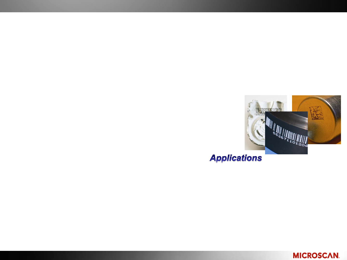
Electrochemical (chem etch)
Electrical current passes through a stencil into the conductive metal part
Material is not weakened or distorted
Good for thin or fragile material
Can produce toxic fumes
- Military
- Aerospace
- Medical device
Advantage:
- Permanent
- High quality mark
- No debris from process
Disadvantage:
- Potentially toxic material bi-product
- Low-volume use
- Complex process
© 2010 Microscan Systems, Inc.
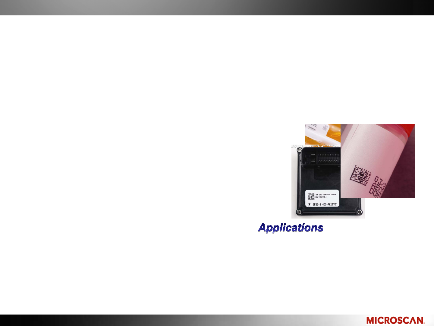
Direct Ink Jet
An ink is applied by spray nozzles, typically resulting in round dots
Food grade inks
Quality and contrast varies
Print on difficult shapes
Marking Methods
- Post-packaging
- Warehousing
- Automotive
- Bio-science
- Pharmaceuticals
- Packaging
- Clinical R&D
- Electronics
Advantage:
- High contrast if done right
- Low entry cost
-No damage to part surface
-High speed printing
Disadvantage:
-Temporary in most cases
-Easy to make a poor print
-Contrast varies
-Consumables (ink)
© 2010 Microscan Systems, Inc.
Marking Methods
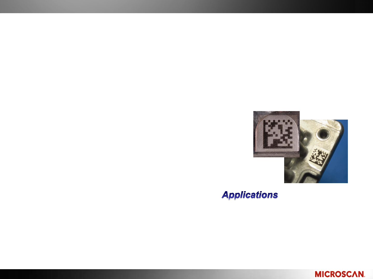
Laser Etch: Anneal, Ablation
Laser is used to cut away a thin layer of surface material.
Ablation exposes another material for higher contrast.
Anneal heats a Materials surface to alter its composition.
-Aerospace
-Military
-Automotive
-Electronics
-Surgical tools
-Medical Implants
Advantage:
-Clean, high resolution
-Can be high contrast
-Permanent (if not using labels)
-No consumables (if not using labels)
-Does not alter part surface (anneal)
Disadvantage:
-Possible consumables (if using labels)
-Affects surface integrity
-Process creates debris
© 2010 Microscan Systems, Inc.
Dot Peen
A multi-axis pointed stylus hits a part like a hammer, which displaces
material, leaving a dimple in its place
Typically used on metals
Recommended for automotive and aerospace
where the marks must last the life of the part
Marking Methods
-Automotive
- Aerospace
- Military
Advantage:
- Permanent
-No consumables
Disadvantage:
- Alters surface
- Low contrast mark
- More difficult to read
- Inconsistent depth will create smaller elements
- Background noise

© 2010 Microscan Systems, Inc.
DECODING 2D SYMBOLS
© 2010 Microscan Systems, Inc.
Capture an Image
A light source is used to illuminate the part
A sensor captures the reflected light and converts to a digital image
Software is used to decode the image

© 2010 Microscan Systems, Inc.
Decoding a 2D Symbol
Decoding consists of two parts:
Locate
Decoder must locate the symbol within the image using unique traits to
each symbology
A higher resolution sensor will take longer to locate
It will take longer to locate a symbol in a noisy field of view
Decode
Decoding algorithms are unique to the products you are using
When a decoder is configured to look for several symbologies, decode time
will be longer
A minimum number of Pixels Per Element (PPE) will ensure consistent
decodes
© 2010 Microscan Systems, Inc.
Decoding a 2D Symbol
Pixels Per Element (PPE)
•The number of pixels that cover an element in either the X or Y dimension.
•The number of Pixels Per Element is determined by:
• Symbol size (size of the elements)
• Camera resolution (sensor size)
•Field of view (optics)
2 Pixels per
Element
One Element
Microscan’s read range tables have this calculated for you.
© 2010 Microscan Systems, Inc.
Maximizing Readability
Consider the following when designing a code:
Contrast: maximize the difference between white and black elements
–Easier to read
–No special lighting or algorithms
Quiet Zone: increase the Quiet Zone to improve decode speeds
Element size: the larger the better for DPM
–Overcome surface texture (DPM)
–More versatile with reading equipment
Quality: good codes decode more reliable
–Damaged codes use error correction
–Improperly marked codes reduce contrast
Mark position: choose a smooth flat location
–Avoid curved or bumpy surfaces if possible
–Position where it is accessible by a reader
A nicely printed Dot Peen
can be easy to read
© 2010 Microscan Systems, Inc.
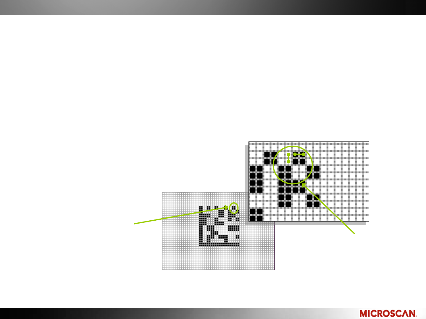
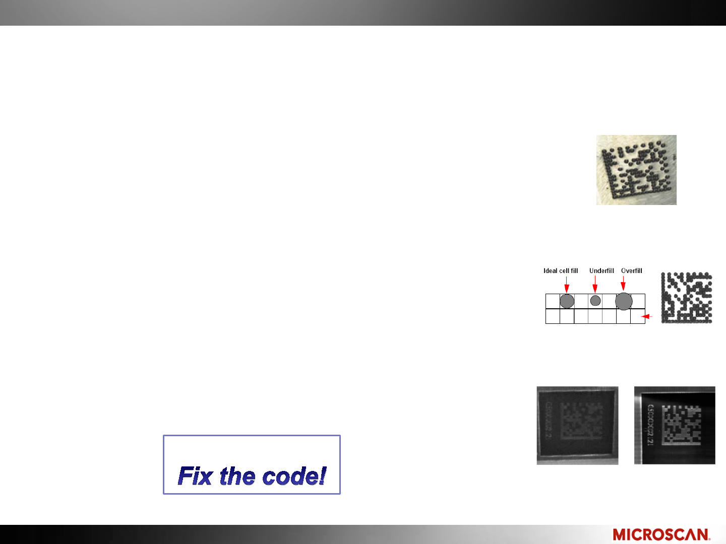
Decodability
Common problems with Direct Part Marks
Dot center offset
–The elements do not have a consistent placement
Cell fill
–The percentage that an element fills its ideal size
–Slight underfill is typically more readable than overfill
Contrast
–Low contrast can be a problem on DPMs
–Adjust the imager and lighting angles to optimize
Dot center offset
Contrast
Cell fill
The best solution:
© 2010 Microscan Systems, Inc.
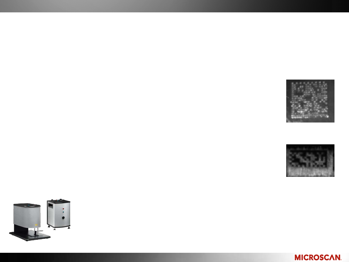
Decodability
Common problems with Direct Part Marks
Modulation
–Uneven printing or illumination can make it difficult to
read a code
–Adjust the imager and lighting angles to optimize
Quiet Zone (Margin) violations
–A poor Quiet Zone may make it hard to locate a code
Verification prevents these errors
Modulation
Poor quiet zone
Verifiers
Microscan’s LDP and DPM Verifiers provide complete reports to current
Data Matrix verification standards for printed and Direct Part Marks.
ISO/IEC 16022 • ISO/IEC 15415 • AS9132 • AIM DPM Guidelines • MIL-STD-130
© 2010 Microscan Systems, Inc.
© 2010 Microscan Systems, Inc.
Decodability
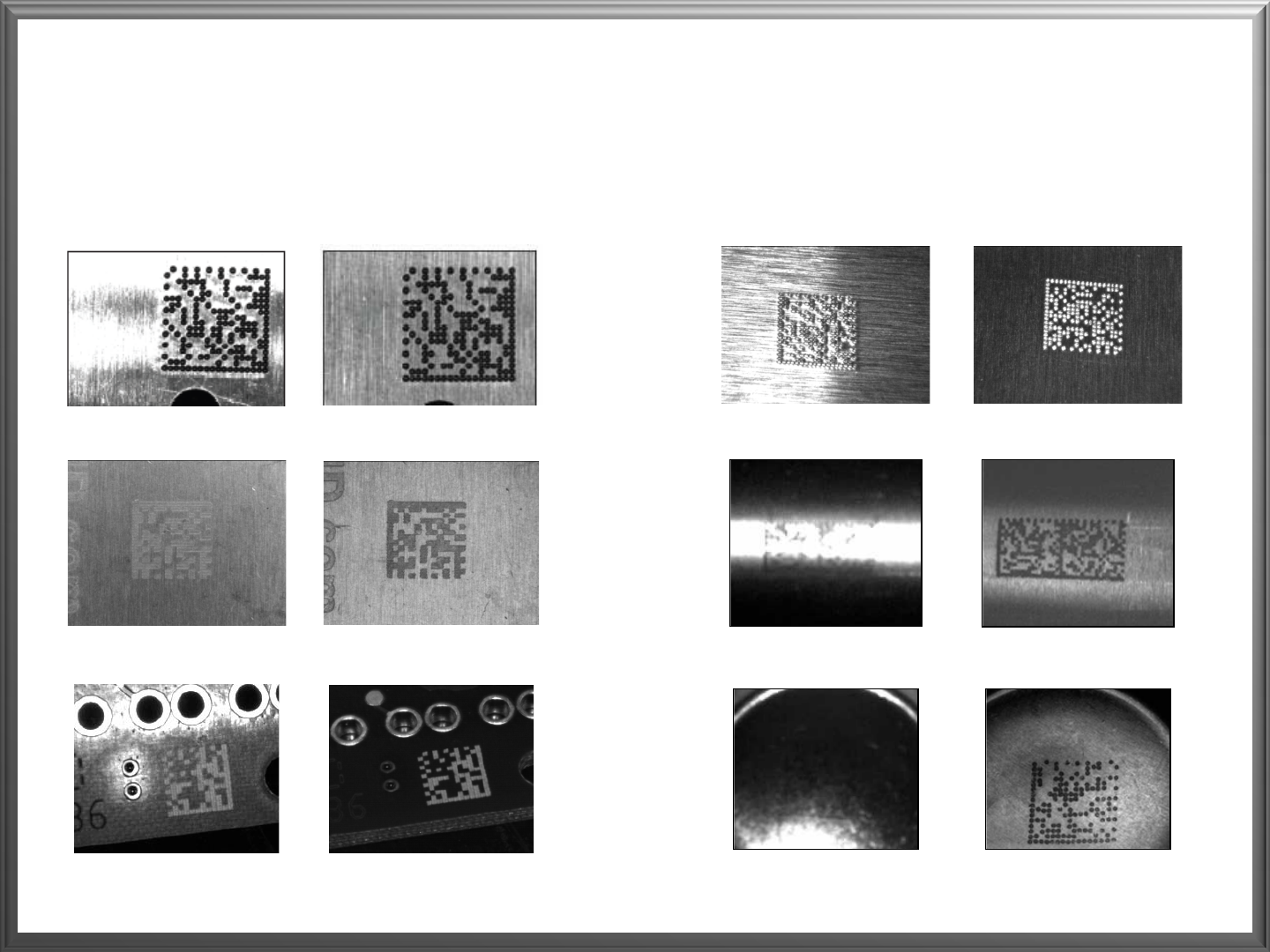
Example images on Direct Part Marks
Before After Before After
Effect of surface structure: rotate 90°
Effect of curved surface: use external line light
Effect of concave surface: use dome light
Effect of shiny surface: use diffuser
Effect of reading angle: change reading angle
Effect of low contrast: change reading angle

© 2010 Microscan Systems, Inc. © 2010 Microscan Systems, Inc.
Marking & Decoding 2D Symbologies
Conclusion
Marking Methods
–Printed
–Chem Etch
–Direct Ink Jet
Decoding a 2D symbology
–Locate, and then decode
–Minimum resolution (PPE)
Maximizing Readability and Decodability
–Making a better image will improve reliability
–Laser Anneal, Ablation, Etch
–Dot Peen

© 2010 Microscan Systems, Inc. © 2010 Microscan Systems, Inc.
Next session….
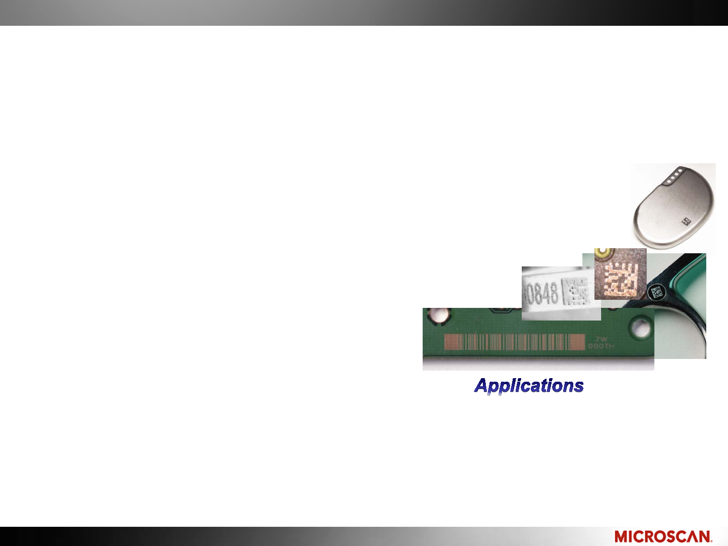
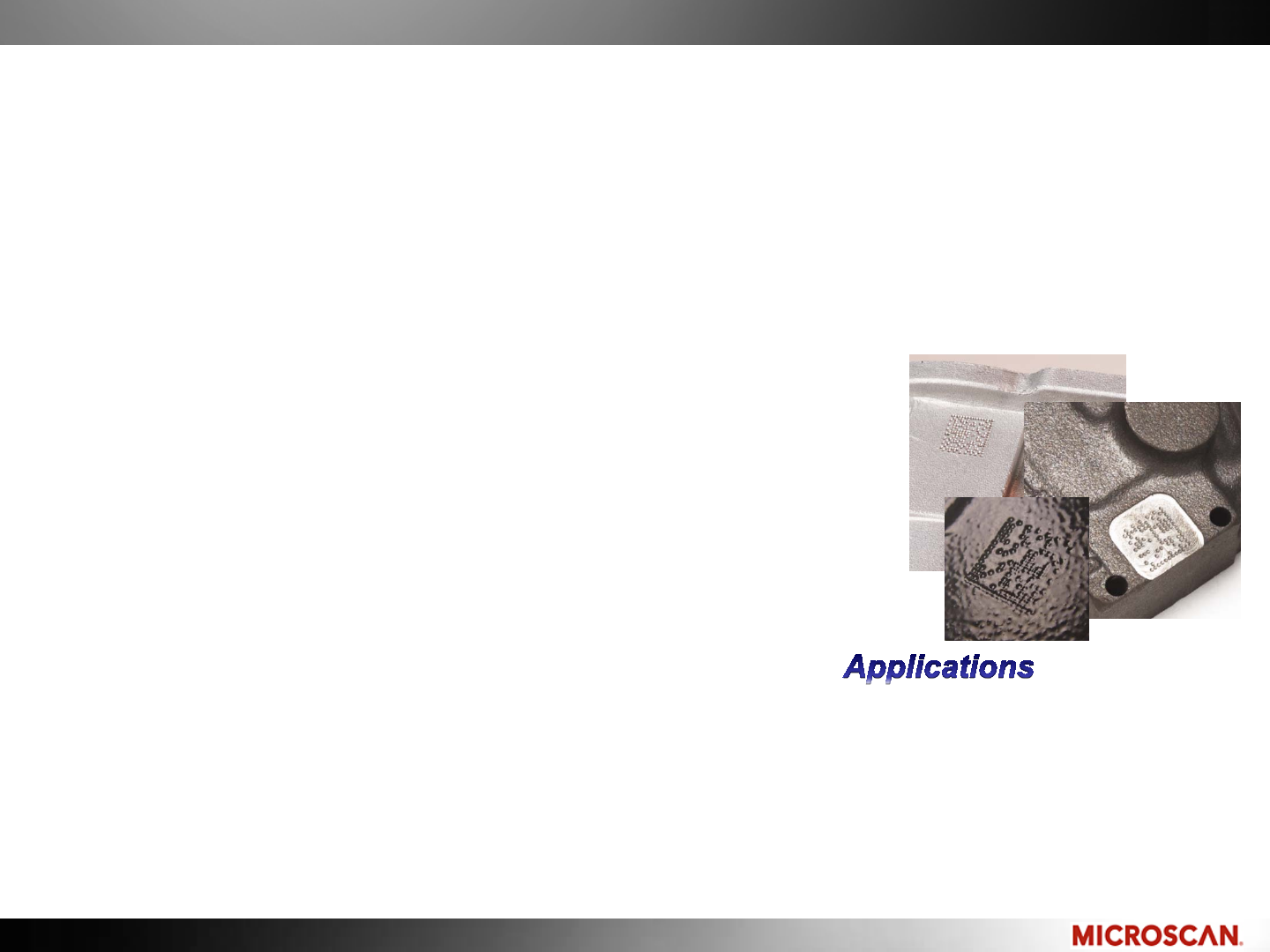
Applications and technology:
Data Matrix applications in vertical markets
Reading technology for applications

© 2010 Microscan Systems, Inc.
Thank you!
For More information
Website: www.microscan.com
–Online courses
–Spec sheets
–Technology brochures
–Support self-help and support request form
Webinar feedback: www.microscan.com/feedback
Instructors:
Juan Worle, Technical Training Coordinator
Email: jworle@microscan.com
Matt Van Bogart, Global Channel Manager
Email: mvanbogart@microscan.com
