Readability Of Directly Marked Traceability Symbols On PCBs
2017-02-06
: Microscan Readability Of Directly-Marked Traceability Symbols On Pcbs Readability of Directly-Marked Traceability Symbols on PCBs WhitePapers PartnerSite
Open the PDF directly: View PDF ![]() .
.
Page Count: 5
READABILITY OF DIRECTLY-MARKED TRACEABILITY SYMBOLS ON
PCBs
Christoph Wimmer, Steven Moser, Tim O’Neel, Leah Sun Zhen
Microscan
Renton, WA 98057
cwimmer@microscan.com
Keywords:
Traceability, PCB, DPM
INTRODUCTION:
Compliance with ISO 9001 and lean PCB manufacturing
relies heavily on traceability data to assist with inventory
control, automatic machine setup, warranty claims,
optimization of production capabilities, and reduction of
waste in terms of material handling and material scrap.
Requirements from the military, aerospace, automotive, and
medical device industries make it essential to be able to
identify individual panels, boards, and parts at each
production step. Recent recalls have shown how important it
is to have this data available to reduce recall costs. The most
widely-used method has been manual application of labels.
Keeping up with modern production capabilities can be a
challenge, and most companies are now transitioning to inkjet
or laser marking. The goal is to apply markings that can be
read throughout the overall process and by the end-customer,
and can also be relied upon in the case of recalls and recycling
programs.
BARCODES
It is critically important to choose the right barcode size and
type, since the part number, supplier code, manufacturing
traceability data, environmental information, and
occasionally even country of origin need to be encoded. Due
to limitations of board and component space, several
manufacturers are moving from 1D to 2D symbologies to
take advantage of the higher data density (Table 1). Data
Matrix (DM) ECC 200 symbols are preferred for their robust
built-in error correction, which ensures readability even if as
much as 50% of the symbol is obstructed. There are several
standards concerning PCB identification. The main ones are
ANSI/EIA 706 and EIA PN 3497. These standards describe
how components like PCBs, parts, and populated PCBs need
to be marked. This paper focuses specifically on 2D Direct
Part Mark (DPM) symbols covered in these standards.
Table 1 – Data Capacity of Square DM Symbols
Square
Data Capacity
Symbol Size
Numeric
Alphanumeric
48x48
348
259
52x52
408
304
64x64
560
418
72x72
736
550
80x80
912
682
88x88
1152
862
Table 2 – Data Capacity of Rectangular DM Symbols
Rectangular
Data Capacity
Symbol Size
Numeric
Alphanumeric
8x18
10
6
8x32
20
13
12x26
32
22
12x36
44
31
16x36
64
46
16x48
98
72
MARKING METHODS
Most PCB manufacturers use one of four methods to mark
PCB boards and panels:
Inkjet printer
Labels
Laser marker
Laser marker with silkscreen pad
Each of these marking methods have advantages in certain
situations. There are still instances of older application
designs using labels for individual marking due to easier
readability, better code quality, or customer requirements.
The comparison (Table 2) doesn’t include the laser silkscreen
pad as it is very similar to laser marking. The pad is normally
applied by the PCB manufacturer and provides better contrast
than direct marks:
Table 3 – Marking Methods
Inkjet
Label
Laser
Easy
Changeover
Yes
No
Yes
Speed
Good
Manual
application
method can
slow down
process
Good
Operating
Costs
Medium
High
Low
Consumable
s
~1.7ct/mar
k
3-10ct/label
~0.03ct/ma
rk
Permanence
Permanent
after wave
solder or
curing
Can be
removed
Will last as
long as the
surface
integrity
Maintenance
Weekly
NA
Monthly
Code quality
A-D
A-C
A-D
Color
Yes
Yes
No
Most new SMT lines use laser marking systems at the
beginning of the production process, as they allow permanent
individual board marking, easy changeover at high speeds,
and low operating costs. PCBs can be marked with either
CO2, YAG, or fiber lasers. Of these types of lasers, fiber
lasers produce the best edge definition and have highly
accurate depth control, but they are also the most expensive.
For the best marking results, it is necessary to optimize pulse
energy, pulse duration, and repetition rate.
VERIFICATION VS. VALIDATION
It is becoming increasingly critical to add a verification step
into the manufacturing system to help achieve the benefits of
data capture and to ensure readability throughout the supply
chain. Automated data capture is crucial for a company’s
success, as the results of decode failures can have a serious
impact. Additionally, verification can be used to monitor how
well the label printer or direct part marking equipment is
performing, and reduce the risk of manufacturing errors or
downtime caused by unreadable codes. Verification catches
deteriorations in the marking process early so that
countermeasures can be employed before unacceptable
product enters the production line. This helps manufacturers
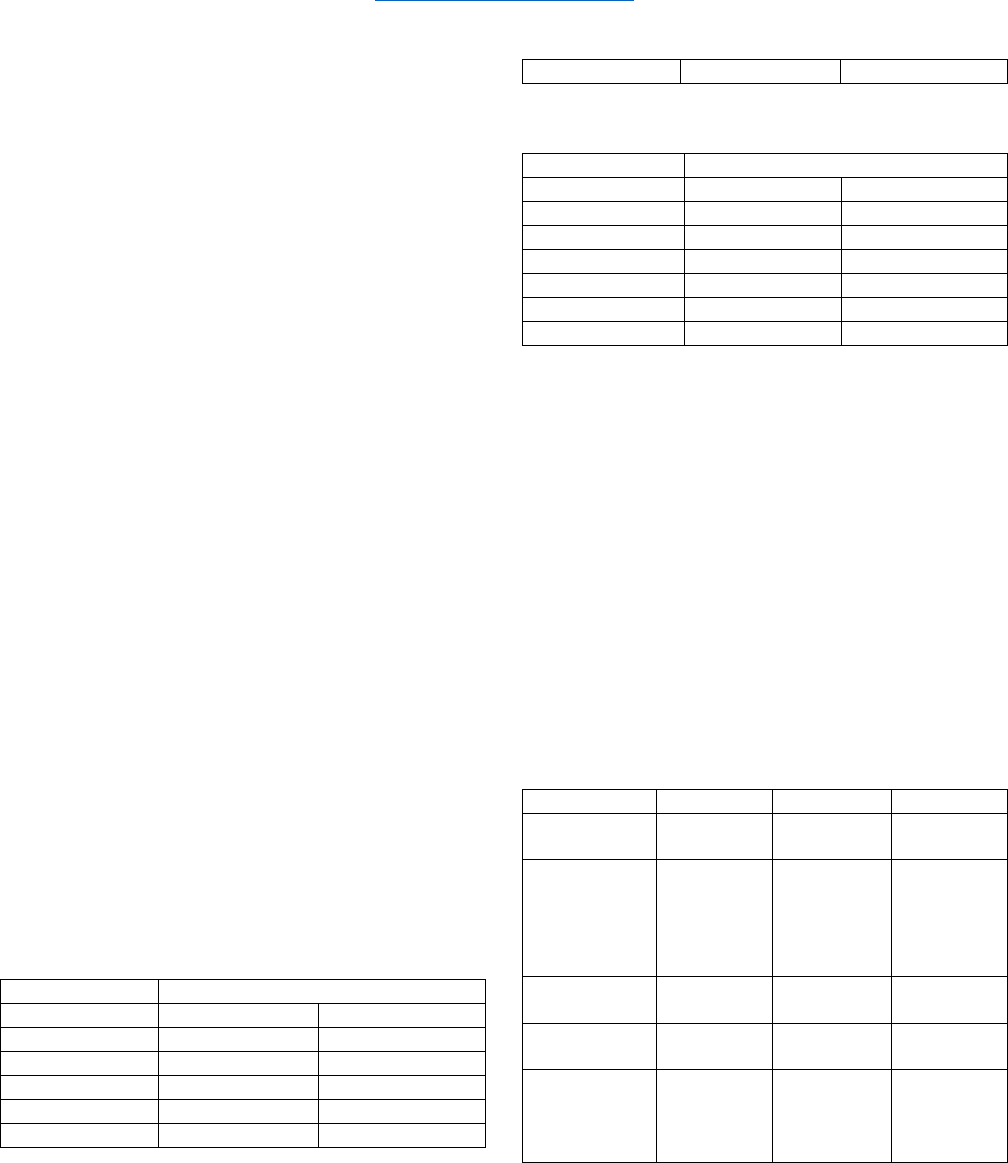
avoid rejections of product by the end customer (Figure 1).
Figure 1: Impact of Symbol Verification
Many manufacturers validate readability by using a reader to
ensure that that a code is readable. But this doesn’t ensure
that it can be read by other readers later in the production
process. True verification provides information about how
well the code can be read and can provide indications about
printing and marking process stability. Verification ensures
that any correctly-functioning reader can decode the given
symbol. Verification is either keyed to an internal standard to
ensure process stability, or to one of the following standards:
- ISO 15415/ISO 29158: 2D Symbols
- AS9132: 2D symbols
Verification is performed by camera-based systems with
specific lighting, and results come in the form of a grade,
from A (perfect) to F (least likely to be decodable by most
readers). ISO 15415 is for printed labels while ISO 29158 is
for directly-marked parts. The following evaluation
parameters are measured specifically for ISO 15415 and ISO
29158:
Axial Non-Uniformity (ISO 15415/ISO 29158)
Axial Non-Uniformity is the amount of deviation along the
symbol’s major axes. In Figure 2 (A), the symbol’s Y-axis
dimension is clearly greater than its X-axis dimension. This
indicates that the marking process is resulting in the Y-
dimensions of individual modules being greater than their X-
dimensions. This inconsistency of X- and Y-dimensions
typically indicates movement of the object as it is being
marked.
Symbol Contrast (ISO 15415)
Symbol Contrast is the value difference between light and
dark symbol elements, and between the quiet zone and
perimeter elements. Figure 2 (B) shows a low-contrast
symbol. The dark elements (etched) and the light elements
(the substrate) are too close in value, which undermines
readability.
Cell Contrast (ISO 29158)
Cell Contrast is the value difference between light and dark
symbol elements, and between the quiet zone and perimeter
elements. Figure 2 (C) shows a low-contrast direct part mark
symbol. The light and dark elements are too close in value,
which undermines readability.
Modulation (ISO 15415)
Modulation refers to the reflectance uniformity of a symbol’s
light and dark elements. In Figure 2 (D), notice that the light
and dark values of some elements are inconsistent.
Cell Modulation (ISO 29158)
Cell Modulation refers to the reflectance uniformity of a
symbol’s light and dark elements. In Figure 2 (E), notice that
the light and dark values of some of the elements in the dot
peen mark are inconsistent.
Decodability (ISO 15415/ISO 29158)
Decodability refers to a symbol’s ability to be decoded per a
standard reference decode algorithm. Figure 2 (F) shows a
high-quality 2D symbol.
Fixed Pattern Damage (ISO 15415/ISO 29158)
Fixed Pattern Damage refers to finder pattern and clock
pattern damage. Notice the missing elements in the clock
pattern and the damaged L-pattern in Figure 2 (G).
Grid Non-Uniformity (ISO 15415/ISO 29158)
Grid Non-Uniformity refers to a symbol’s cell deviation from
the ideal grid of a theoretical “perfect symbol”. The Data
Matrix reference decode algorithm is applied to a binarized
image of the symbol, comparing its actual grid intersections
to ideal grid intersections. The greatest distance from an
actual to a theoretical grid intersection determines the Grid
Non-Uniformity grade. The symbol shown in Figure 2 (H)
exhibits a high degree of Grid Non-Uniformity.
Minimum Reflectance (ISO 29158)
Minimum Reflectance refers to the minimum reflectance of
light by the symbol’s light elements. In Figure 2 (I), notice
that the symbol’s light elements exhibit a minimum
reflectance to ensure contrast against the dark substrate to
allow readability.
Reflectance Margin (ISO 15415)
Reflectance Margin measures how well each element of a
symbol is correctly distinguishable as light or dark in
comparison to the global threshold. Low reflectance margin,
such as that illustrated in Figure 2 (J), may increase the
probability that a symbol element will be incorrectly
identified as dark or light.
Unused Error Correction (ISO 15415/ISO 29158)
Unused Error Correction indicates the amount of available
Error Correction in a symbol. Error Correction is a method of
reconstructing or replacing data that is lost through symbol
damage. 100% Unused Error Correction is ideal, as shown in
Figure 2 (K).
Over- and under-print can also occur, causing symbol
decodability problems.
(A) Axial Non-
Uniformity
(B) Symbol
Contrast
(C) Cell
Contrast
(D) Modulation
(E) Cell
Modulation
(F) Decodability
(G) Fixed
Pattern Damage
(H) Grid Non-
Uniformity
(I) Minimum
Reflectance
(J) Reflectance
Margin
(K) Unused Error
Correction
Figure 2: Verification Evaluation Parameters
Symbol verification immediately following the printing or
marking process ensures proper readability throughout the
application, and can help with the setup of the inkjet or laser
marker. These systems must be properly calibrated with
specialized calibration cards if verifying to the ISO 15415 or
ISO 29158 standard.
1D/2D READERS
Modern barcode readers use a variety of techniques to ensure
that codes can be read properly. These readers can either
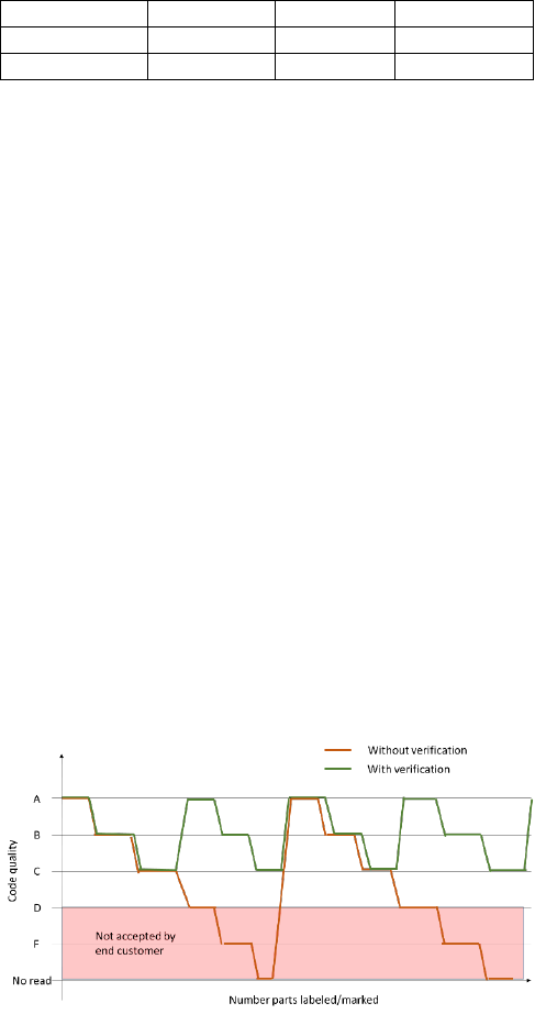
come in a handheld or fixed-mount form. Figure 3 shows the
components of a compact fixed-mount reader.
Figure 3: 2D Reader Components
Lighting
The lighting system ensures maximum symbol reflectance.
For optimal performance, proper mounting of the reader is
essential. The reader is normally positioned 30° to 45°
perpendicular to the symbol. The more powerful the lighting
system, the more accurately low-contrast symbols can be
decoded.
Lens System and CCD/CMOS Sensor
The lens system, in combination with the CCD/CMOS
sensor, ensures that codes as small as 2.5 mil can be decoded
at the required reading distance. Readers typically come with
specification charts that show field of view, depth of field,
and minimum readable symbol size. Additional features such
as autophotometry may also be available, allowing you to
adapt gain and shutter speed automatically. Autophotometry
optimizes image exposure and allows readability of codes on
variously-colored PCBs.
Processor
The processor runs the decoding software with advanced
algorithms, allowing the reader to decode difficult-to-read
symbols.
Memory
The reader’s memory can be used to store no-read images for
further analysis.
Interface
RS-232, USB, or Ethernet are most commonly used. Various
industrial protocols such as EtherNet/IP and PROFINET can
be supported by modern barcode readers.
Configuration Software
Traditionally, users must download and install specialized
configuration software to make reader parameter
modifications. Modern readers can leverage web browser
technology for configuration and testing. By simply entering
the IP address on any web-enabled device, all reader
parameters can be configured. This means that no software
needs to be installed. Browser-based configuration programs
support different operating systems (Windows, MacOS, iOS,
Android) and run on any web-enabled device (PC, tablet,
phone). Intuitive user interfaces limit the amount of clicks
necessary to start decoding (Figure 4).
Figure 4: Web-Based Configuration Software Results
RESULTS:
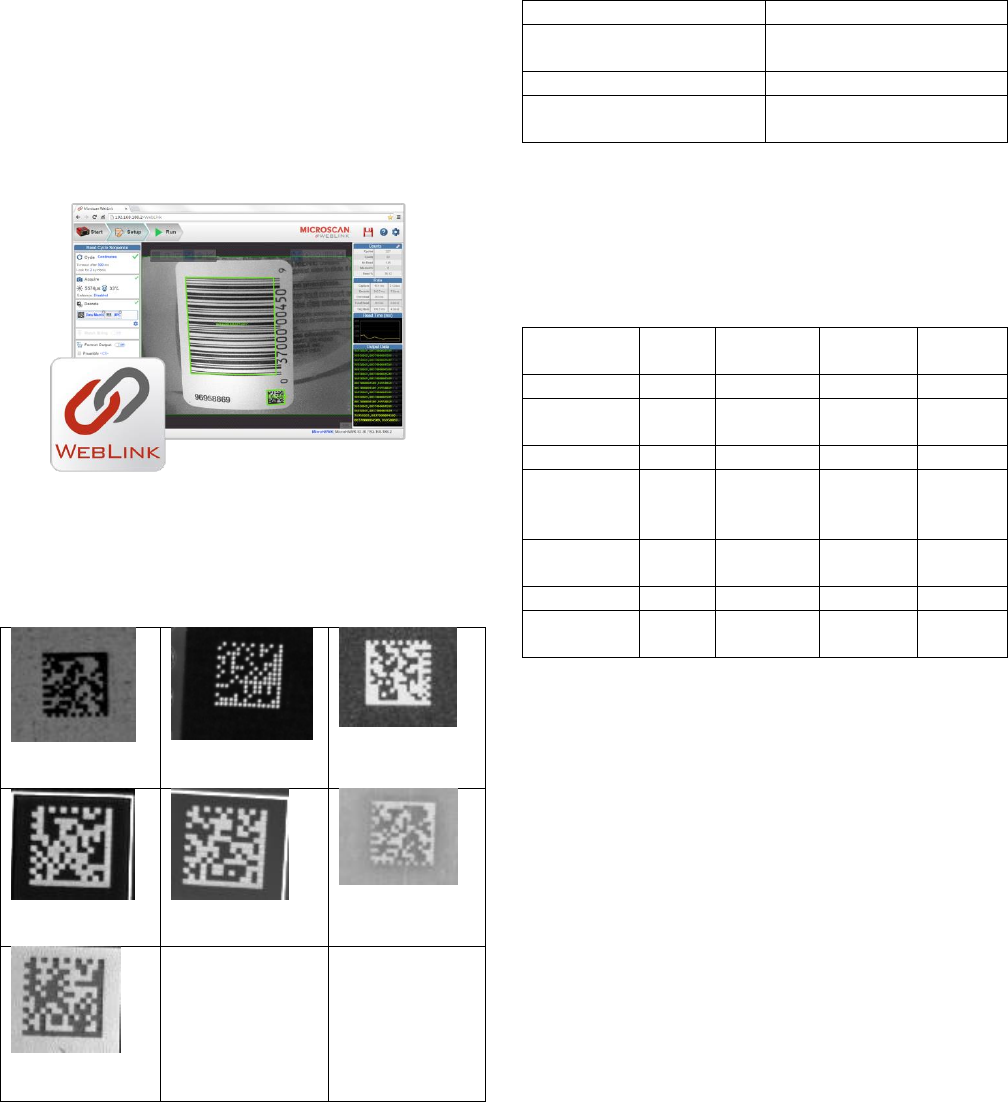
We tested 2D readers on different colored boards that were
laser marked with 5mil (0.127mm) codes:
(A) Black PCB
(B) Black
Silkscreen
(C) Blue PCB
(D) Copper on
Green PCB
(E) Green PCB
(F) Red PCB
(G) White
Silkscreen
Figure 5: Tested Boards
First we used a UID DPM verifier and verified the codes
according to ISO 29158. As expected, these were high-
quality codes, the only exception being the code on the red
board which was Grade B due to lower cell contrast and fixed
pattern damage. We tested comparable, standard, off-the-
shelf, second generation miniature readers from different
vendors. The first test was to unpack the reader, download
and install software, connect, and power up the reader.
Setup Time
Reader 1
2 min. (Web-based
configuration)
Reader 2
19 min.
Reader 3
28 min. (6 min. to find the
right software to install)
Placement of the code was slightly easier with reader 1 as it
had a larger field of view (21.7 cm2 vs. 10.6 cm2 for reader 2
and 4.2 cm2 for reader 3). Additionally, the web-based user
interface was much more intuitive. The next step was to try
to read the codes on the PCBs without any additional
adjustments.
Grade
Reader 1
Reader 2
Reader
3
Black PCB
A
Yes
Yes
Yes
Black
Silkscreen
A
Yes
Yes
Yes
Blue PCB
A
Yes
Yes
Yes
Copper on
Green
PCB
A
Yes
Yes
Yes
Green
PCBs
A
Yes
Yes
Yes
Red PCB
B
Yes
No
Yes
White Silk
Screen
A
Yes
Yes
Yes
Two of the readers were able to read all the codes right out of
the box while reader 2 couldn’t read the code on the red
board. This was very likely due to insufficient illumination
provided by the reader. After full adjustment, reader 2 was
still unable to decode the symbol on the red PCB.
CONCLUSION
Modern traceability systems in SMT production lines rely
heavily on proper board marking and advanced readers.
Adding verification directly after the marking process
ensures symbol decodability throughout the application, and
helps with the setup and testing of inkjet or laser markers. As
tests have shown, most readers are capable of handling small
codes on different colored boards. This is essential to
ensuring that proper production data is stored, communicated
throughout the production line, and used in production to
initiate job changes. Tests also show that web-based
configuration software has an immediate advantage as no
software has to be installed, there is no need to worry about
version conflict, and any computer can run the web-based
configuration user interface.
REFERENCES
[1] Understanding 2D Verification, Microscan 2013
[2] Direct Product Marking for PCB Identification, Jetec
2004
[3] Laser Marking Technologies, Sintec Optronics,
[4] Ink Jet Systems, Jetec Corp.
[5] J. Sercel and U. Sowada, Why excimer lasers excel in
marking, Lasers & Optronics, Vol. 7, No. 9 (1988), 69-72
[6] T. J. McKee, How lasers mark, ElectroTechnology, Vol.
7, No. 2 (1996), 27-31
[7] S. J. Parnas, Indelible coding with lasers: variable
information marking on-the-fly, Surface Mount Technology,
Dec. 1989, 20-28
[8]J. F. Higgins, Laser marking of passive components,
hybrids and semiconductors, Proc. of SPIE Vol. 611 Laser
Processing of Semiconductors and Hybrids (1986), 40-47
[9]Cucu, T.C., 1D and 2D solutions for traceability in an
Electronic Manufacturing Services company, Electronics
Technology, 2008. ISSE '08.
[10] Amit Grover, Parameters Effecting 2D Barcode
Scanning Reliability, Advances in Computers Volume 80,
2010, Pages 209–235
